EP2713402B1 - Transistor à haute mobilité d'électrons normalement bloqué - Google Patents
Transistor à haute mobilité d'électrons normalement bloqué Download PDFInfo
- Publication number
- EP2713402B1 EP2713402B1 EP13173455.0A EP13173455A EP2713402B1 EP 2713402 B1 EP2713402 B1 EP 2713402B1 EP 13173455 A EP13173455 A EP 13173455A EP 2713402 B1 EP2713402 B1 EP 2713402B1
- Authority
- EP
- European Patent Office
- Prior art keywords
- depletion
- layer
- forming layer
- normally
- hemt
- Prior art date
- Legal status (The legal status is an assumption and is not a legal conclusion. Google has not performed a legal analysis and makes no representation as to the accuracy of the status listed.)
- Active
Links
Images


Classifications
-
- H—ELECTRICITY
- H10—SEMICONDUCTOR DEVICES; ELECTRIC SOLID-STATE DEVICES NOT OTHERWISE PROVIDED FOR
- H10D—INORGANIC ELECTRIC SEMICONDUCTOR DEVICES
- H10D30/00—Field-effect transistors [FET]
- H10D30/40—FETs having zero-dimensional [0D], one-dimensional [1D] or two-dimensional [2D] charge carrier gas channels
- H10D30/47—FETs having zero-dimensional [0D], one-dimensional [1D] or two-dimensional [2D] charge carrier gas channels having two-dimensional [2D] charge carrier gas channels, e.g. nanoribbon FETs or high electron mobility transistors [HEMT]
-
- H—ELECTRICITY
- H10—SEMICONDUCTOR DEVICES; ELECTRIC SOLID-STATE DEVICES NOT OTHERWISE PROVIDED FOR
- H10P—GENERIC PROCESSES OR APPARATUS FOR THE MANUFACTURE OR TREATMENT OF DEVICES COVERED BY CLASS H10
- H10P10/00—Bonding of wafers, substrates or parts of devices
-
- H—ELECTRICITY
- H10—SEMICONDUCTOR DEVICES; ELECTRIC SOLID-STATE DEVICES NOT OTHERWISE PROVIDED FOR
- H10D—INORGANIC ELECTRIC SEMICONDUCTOR DEVICES
- H10D30/00—Field-effect transistors [FET]
- H10D30/40—FETs having zero-dimensional [0D], one-dimensional [1D] or two-dimensional [2D] charge carrier gas channels
- H10D30/47—FETs having zero-dimensional [0D], one-dimensional [1D] or two-dimensional [2D] charge carrier gas channels having two-dimensional [2D] charge carrier gas channels, e.g. nanoribbon FETs or high electron mobility transistors [HEMT]
- H10D30/471—High electron mobility transistors [HEMT] or high hole mobility transistors [HHMT]
- H10D30/475—High electron mobility transistors [HEMT] or high hole mobility transistors [HHMT] having wider bandgap layer formed on top of lower bandgap active layer, e.g. undoped barrier HEMTs such as i-AlGaN/GaN HEMTs
-
- H—ELECTRICITY
- H10—SEMICONDUCTOR DEVICES; ELECTRIC SOLID-STATE DEVICES NOT OTHERWISE PROVIDED FOR
- H10D—INORGANIC ELECTRIC SEMICONDUCTOR DEVICES
- H10D62/00—Semiconductor bodies, or regions thereof, of devices having potential barriers
- H10D62/10—Shapes, relative sizes or dispositions of the regions of the semiconductor bodies; Shapes of the semiconductor bodies
- H10D62/17—Semiconductor regions connected to electrodes not carrying current to be rectified, amplified or switched, e.g. channel regions
- H10D62/343—Gate regions of field-effect devices having PN junction gates
-
- H—ELECTRICITY
- H10—SEMICONDUCTOR DEVICES; ELECTRIC SOLID-STATE DEVICES NOT OTHERWISE PROVIDED FOR
- H10D—INORGANIC ELECTRIC SEMICONDUCTOR DEVICES
- H10D62/00—Semiconductor bodies, or regions thereof, of devices having potential barriers
- H10D62/80—Semiconductor bodies, or regions thereof, of devices having potential barriers characterised by the materials
- H10D62/85—Semiconductor bodies, or regions thereof, of devices having potential barriers characterised by the materials being Group III-V materials, e.g. GaAs
- H10D62/8503—Nitride Group III-V materials, e.g. AlN or GaN
-
- H—ELECTRICITY
- H10—SEMICONDUCTOR DEVICES; ELECTRIC SOLID-STATE DEVICES NOT OTHERWISE PROVIDED FOR
- H10D—INORGANIC ELECTRIC SEMICONDUCTOR DEVICES
- H10D64/00—Electrodes of devices having potential barriers
- H10D64/111—Field plates
-
- H—ELECTRICITY
- H10—SEMICONDUCTOR DEVICES; ELECTRIC SOLID-STATE DEVICES NOT OTHERWISE PROVIDED FOR
- H10D—INORGANIC ELECTRIC SEMICONDUCTOR DEVICES
- H10D64/00—Electrodes of devices having potential barriers
- H10D64/20—Electrodes characterised by their shapes, relative sizes or dispositions
- H10D64/27—Electrodes not carrying the current to be rectified, amplified, oscillated or switched, e.g. gates
- H10D64/311—Gate electrodes for field-effect devices
- H10D64/411—Gate electrodes for field-effect devices for FETs
Definitions
- the invention relates to a normally-off high electron mobility transistor (HEMT), and more particularly, to a normally-off HEMT including a depletion-forming layer.
- HEMT normally-off high electron mobility transistor
- Various power conversion systems may include a device for controlling a current flow by ON/OFF switching thereof, e.g., a power device.
- the efficiency of a power conversion system may depend on the efficiency of a power device in the power conversion system.
- MOSFETs Metal-Oxide-Semiconductor Field-Effect Transistors
- IGBTs Insulated Gate Bipolar Transistors
- a HEMT may include semiconductor layers having different electrical polarization characteristics.
- a semiconductor layer having a relatively high polarization rate may induce a two-dimensional electron gas (2DEG) in another semiconductor layer attached thereto, and the 2DEG may have very high electron mobility.
- 2DEG two-dimensional electron gas
- a gate voltage of a HEMT When a gate voltage of a HEMT is 0 V, power consumption may occur in a normally-on state in which a current flows between drain and source electrodes thereof due to a low resistance therebetween. To change to a normally-off state in which no current flows between the drain and source electrodes, a negative voltage may be applied to a gate electrode of a HEMT.
- a HEMT having a depletion-forming layer to implement a normally-off characteristic by which no current flows between drain and source electrodes of the HEMT when a gate voltage thereof is 0 V has been researched.
- US 2010/097105 teaches a semiconductor device capable of a bi-directional switching operation used for power control.
- Depletion-forming layers disclosed therein may include protruding portions.
- the invention relates to a normally-off high electron mobility transistor (HEMT) using a depletion-forming layer.
- HEMT normally-off high electron mobility transistor
- HEMT normally-off high electron mobility transistor
- the first part of the depletion-forming layer may be a strip shape
- the second part and third part may be a strip shape in parallel to the first part
- the gate electrode is on the gate insulation layer above at least a portion of the first to third parts of the depletion-forming layer.
- the gate insulating layer defines an opening that exposes a portion of the depletion-forming layer, and the gate electrode contacts the depletion-forming layer through the opening.
- the opening is on the first part of the depletion-forming layer.
- the first nitride semiconductor may include a gallium nitride (GaN) group material.
- GaN gallium nitride
- the second nitride semiconductor may include a nitride that includes at least one of aluminum (Al), gallium (Ga), indium (In) and boron (B).
- the depletion-forming layer may include a p-type nitride semiconductor.
- the depletion-forming layer may include a III-V group nitride semiconductor material.
- example embodiment is used to refer to subject-matter according to the present invention, whereas the term “example” is used to refer to subject-matter not covered by the claims.
- Example embodiments will now be described more fully with reference to the accompanying drawings, in which some example embodiments are shown.
- Example embodiments may, however, be embodied in many different forms and should not be construed as being limited to the embodiments set forth herein; rather, these example embodiments are provided so that this disclosure will be thorough and complete, and will fully convey the scope of example embodiments to those of ordinary skill in the art.
- the thicknesses of layers and regions are exaggerated for clarity.
- Like reference numerals in the drawings denote like elements, and thus their description may be omitted.
- first, second, etc. may be used herein to describe various elements, components, regions, layers and/or sections, these elements, components, regions, layers and/or sections should not be limited by these terms. These terms are only used to distinguish one element, component, region, layer or section from another element, component, region, layer or section. Thus, a first element, component, region, layer or section discussed below could be termed a second element, component, region, layer or section without departing from the teachings of example embodiments.
- spatially relative terms such as “beneath,” “below,” “lower,” “above,” “upper” and the like, may be used herein for ease of description to describe one element or feature's relationship to another element(s) or feature(s) as illustrated in the figures. It will be understood that the spatially relative terms are intended to encompass different orientations of the device in use or operation in addition to the orientation depicted in the figures. For example, if the device in the figures is turned over, elements described as “below” or “beneath” other elements or features would then be oriented “above” the other elements or features. Thus, the exemplary term “below” can encompass both an orientation of above and below. The device may be otherwise oriented (rotated 90 degrees or at other orientations) and the spatially relative descriptors used herein interpreted accordingly.
- Example embodiments are described herein with reference to cross-sectional illustrations that are schematic illustrations of idealized embodiments (and intermediate structures) of example embodiments. As such, variations from the shapes of the illustrations as a result, for example, of manufacturing techniques and/or tolerances, are to be expected. Thus, example embodiments should not be construed as limited to the particular shapes of regions illustrated herein but are to include deviations in shapes that result, for example, from manufacturing. Thus, the regions illustrated in the figures are schematic in nature and their shapes are not intended to illustrate the actual shape of a region of a device and are not intended to limit the scope of example embodiments.
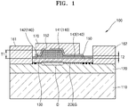
- FIG. 1 is a cross-sectional view schematically showing a structure of a normally-off high electron mobility transistor (HEMT) 100 according to example embodiments.
- HEMT normally-off high electron mobility transistor
- a channel layer 120 is formed on a substrate 110.
- the substrate 110 may be formed of, for example, directed-bonded copper or a semiconductor material such as sapphire, silicon (Si), silicon carbide (SiC), or gallium nitride (GaN).
- Si silicon
- SiC silicon carbide
- GaN gallium nitride
- the channel layer 120 is formed of a first nitride semiconductor material.
- the first nitride semiconductor material may be a group III-V compound semiconductor material.
- the channel layer 120 may be a GaN group material layer.
- the channel layer 120 may be a GaN layer.
- the channel layer 120 may be an undoped GaN layer, and in some cases, the channel layer 120 may be a GaN layer doped with desired (and/or alternatively predetermined) impurities.
- a buffer layer may be further provided between the substrate 110 and the channel layer 120.
- the buffer layer may reduce (and/or prevent) a decrease in crystallizability of the channel layer 120 by alleviating a lattice constant difference and a thermal expansion coefficient difference between the substrate 110 and the channel layer 120.
- the buffer layer may include a nitride including at least one among Al, Ga, In, and B and may have a single-layer structure or a multi-layer structure.
- the buffer layer may be formed of AIN, GaN, AIGaN, InGaN, AlInN, or AlGaInN.
- a seed layer (not shown) for growing the buffer layer may be further provided between the substrate 110 and the buffer layer.
- a channel supply layer 130 is formed on the channel layer 120.
- the channel supply layer 130 induces a two-dimensional electron gas (2DEG) in the channel layer 120.
- the 2DEG may be formed in the channel layer 120 below the interface between the channel layer 120 and the channel supply layer 130.
- the channel supply layer 130 is formed of a second nitride semiconductor material that is different than the first nitride semiconductor material forming the channel layer 120.
- the second nitride semiconductor material may be different from the first nitride semiconductor material with respect to at least one of a polarization characteristic, an energy bandgap, and a lattice constant.
- the second nitride semiconductor material may be higher than the first nitride semiconductor material with respect to at least one of the polarization rate and the energy bandgap.
- the channel supply layer 130 may be formed of at least one nitride that includes at least one among Al, Ga, In, and B and may have a single-layer structure or a multi-layer structure.
- the channel supply layer 130 may be formed of at least one of AIGaN, AlInN, InGaN, AIN, and AlGaInN.
- the channel supply layer 130 may be an undoped layer or a layer doped with desired (and/or alternatively predetermined) impurities.
- the thickness of the channel supply layer 130 may be, for example, less than several tens of nm.
- the thickness of the channel supply layer 130 may be equal to or less than about 50 nm, but the thickness is not limited thereto.
- a source electrode 161 and a drain electrode 162 are formed on the channel layer 120.
- the source electrode 161 and drain electrode 162 are formed at both sides of the channel supply layer 130.
- the source electrode 161 and the drain electrode 162 may be electrically connected to the 2DEG.
- the source electrode 161 and the drain electrode 162 may be formed to be inserted inside the channel layer 120.
- the configuration of the source electrode 161 and drain electrode 162 is not limited thereto.
- the source electrode 161 and the drain electrode 162 may be variously formed.
- a depletion-forming layer 140 is formed on the channel supply layer 130.
- the depletion-forming layer 140 includes a first part 141 having a first thickness T1 and a second part 142 having a second thickness T2 and a third part 143 having the second thickness T2.
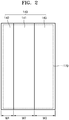
- FIG. 2 is a partial top view of the normally-off HEMT 100 according to example embodiments. In FIG. 2 , some components are omitted for convenience of description.
- the first part 141 may have a strip shape, and the second and third parts 142 and 143 may be formed long at both sides of the first part 141 in a lengthy direction of the first part 141.
- the first part 141 may have a first width W1
- the second part 142 may have a second width W2
- the third part 143 may have a third width W3.
- the first to third widths W1 to W3 may be different from each other.
- the first width W1 may be greater than the third width W3 and the third width W3 may be greater than the second width W2.
- example embodiments are not limited thereto, and the depletion-forming layer 140 may be formed in various shapes.
- at least two of the first to third widths W1 to W3 may be equal.
- the second part 142 is formed to be spaced apart from the source electrode 161 and the third part 143 is formed to be spaced apart from the drain electrode 162.
- the first part 141 may be formed to be closer to the source electrode 161 than the drain electrode 162. However, example embodiments are not limited thereto.
- the depletion-forming layer 140 functions to form a depletion region in the 2DEG.
- An energy bandgap of a portion of the channel supply layer 130, which is located below the depletion-forming layer 140, may increase due to the depletion-forming layer 140, resulting in forming the depletion region of the 2DEG at a portion of the channel layer 120 corresponding to the depletion-forming layer 140.
- the 2DEG may be cut off at a portion corresponding to the first part 141 of the depletion-forming layer 140, and electron density of the 2DEG may decrease at a portion corresponding to the second part 142 and the third part 143 of the depletion-forming layer 140.
- Electron densities of the 2DEG in a region between the depletion-forming layer 140 and the source electrode 161 and a region between the depletion-forming layer 140 and the drain electrode 162 are higher than electron density of the 2DEG below the second part 142 and the third part 143.
- FIG. 1 shows that a region of the 2DEG having relatively high electron density is discriminated from a region of the 2DEG having relatively low electron density by the thicknesses of dots. Electron density is high as dots are thick. A region in which the 2DEG is cut off may be a 'cut-off region', and the normally-off HEMT 100 may have a normally-off characteristic due to the cut-off region.
- the depletion-forming layer 140 may include a p-type semiconductor material. That is, the depletion-forming layer 140 may be a p-type semiconductor layer or a semiconductor layer doped with p-type impurities. In addition, the depletion-forming layer 140 may be formed of a group III-V nitride semiconductor. For example, the depletion-forming layer 140 may be formed of GaN, AIGaN, InN, AlInN, InGaN, or AlInGaN or doped with p-type impurities such as magnesium (Mg). In detail, the depletion-forming layer 140 may be a p-GaN layer or a p-AIGaN layer. The depletion-forming layer 140 may cause an energy bandgap of a portion of the channel supply layer 130 therebelow to increase, thereby forming a cut-off region of the 2DEG or a region having relatively low electron density.
- Mg magnesium
- An insulation layer 150 is formed on the depletion-forming layer 140.
- the insulation layer 150 may be referred to as a gate insulation layer 150 hereinafter.
- the gate insulation layer 150 may be extended to cover the channel supply layer 130.
- the gate insulation layer 150 may be formed to have the thickness of about 50 nm to about 300 nm.
- the gate insulation layer 150 may include at least one among aluminum oxide (Al 2 O 3 ), silicon oxide (SiO x ), silicon nitride (Si x N y ), scandium oxide (Sc 2 O 3 ), aluminum nitride (AIN), gallium oxide (Ga 2 O 3 ), gadolinium oxide (Gd 2 O 3 ), aluminum gadolinium oxide (Al x Gd 2(1-x) O 3 ), aluminum gallium oxide (Al x Ga 2(1-x) O 3 ), magnesium oxide (MgO), and a combination thereof.
- any of insulation materials used for typical transistors may be used as a material for the gate insulation layer 150.
- An opening 152 is formed in the gate insulation layer 150 to expose at least a portion of the surface of the depletion-forming layer 140.
- the opening 152 is formed on the upper surface of the first part 141 of the depletion-forming layer 140.
- the opening 152 may be a through hole, a diameter of which is equal to or less than about 0.25 ⁇ m.
- a gate electrode 170 is formed on the gate insulation layer 150.
- the gate electrode 170 may be arranged above the depletion-forming layer 140 and is formed to contact the depletion-forming layer 140 through the opening 152.
- the gate electrode 170 may be formed to have a narrower area than the depletion-forming layer 140 as shown in FIG. 2 . Since a contact area between the gate electrode 170 and the depletion-forming layer 140 is small (for example less than a width of the gate electrode 170), a leakage current is low and/or may be reduced.
- the gate electrode 170 may include any of various metal materials and metal compounds.
- the depletion-forming layer 140 may be formed to be wider than a region of the gate electrode 170.
- the depletion-forming layer 140 has two thicknesses in FIG. 1 , example embodiments are not limited thereto.
- the depletion-forming layer 140 may have a plurality of thicknesses. A part having the thickest thickness is formed at the central part or formed to be closer to the source electrode 161 at the central part, and the remaining parts have sequentially thinner thicknesses from the central part.
- FIGS. 3A to 3C are cross-sectional views for describing an operation of the normally-off HEMT 100 according to example embodiments.
- a region of the 2DEG having relatively high electron density is discriminated from a region of the 2DEG having relatively low electron density by the thicknesses of dots. Electron density is high as dots are thick.
- FIG. 1 shows a normally-off state of the normally-off HEMT 100.
- a region below the first part 141 is a cut-off region D in which the 2DEG does not exist.
- the 2DEG when a voltage equal to or higher than a threshold voltage is applied to the gate electrode 170, the 2DEG is generated in a cut-off region D, thereby making the normally-off HEMT 100 be in an ON state. That is, a channel formed below the gate electrode 170 is in an ON state, and accordingly, a current flows through the 2DEG formed in the channel layer 120.
- the threshold voltage may vary according to the thickness of the first part 141 of the depletion-forming layer 140 and doping density of the first part 141.
- an area of the depletion-forming layer 140 below the gate electrode 170 increases, resulting in expanding a gate region. Since a contact area between the gate electrode 170 and the depletion-forming layer 140 is small, a leakage current is low.
- the depletion-forming layer 140 is formed to be apart from the source electrode 161, a leakage current path connected from the gate electrode 170 to the source electrode 161 may be blocked.
- FIG. 4 is a cross-sectional view schematically showing a structure of a normally-off HEMT 200 according to an example.
- the same reference numerals are used for the same (and/or substantially the same) components as those in the normally-off HEMT 100 of FIG. 1 , and their detailed description is omitted.
- a depletion-forming layer 240 may be formed on the channel supply layer 130.
- the depletion-forming layer 240 includes a first part 241 having the first thickness T1 and a second part 242 having the second thickness T2, and a third part 243 having the second thickness T2.
- the first part 241 may have a strip shape, and the second part 242 and third part 243 may be formed long at both sides of the first part 241 in a lengthy direction of the first part 241.
- examples are not limited thereto, and the depletion-forming layer 240 may be formed in various shapes.
- the second part 242 may be formed to contact the source electrode 161 and the third part 243 may be formed to contact drain electrode 162.
- the first part 241 may be formed to be closer to the source electrode 161 than the drain electrode 162.
- the second part 242 and third part 243 may be alternatively configured.
- the second part 242 may alternatively be formed similar to the second part 142 in FIG. 1 , which does not contact the source electrode 161.
- the third part 243 may alternatively be formed similar to the third part 143 in FIG. 1 , which does not contact the drain electrode 162.
- one of the second part 242 and the third part 243 may alternatively be arranged so it does not contact an adjacent one of the source electrode 161 and the drain electrode 162.
- the depletion-forming layer 240 may function to form a depletion region in the 2DEG.
- An energy bandgap of a portion of the channel supply layer 130, which is located below the depletion-forming layer 240, may increase due to the depletion-forming layer 240, resulting in forming the depletion region of the 2DEG at a portion of the channel layer 120 corresponding to the depletion-forming layer 240.
- the 2DEG may be cut off at a portion corresponding to the first part 241 of the depletion-forming layer 240, and electron density of the 2DEG may decrease at a portion corresponding to the second part 242 and the third part 243 of the depletion-forming layer 240.
- FIG. 4 shows that a region of the 2DEG having relatively high electron density is discriminated from a region of the 2DEG having relatively low electron density by the thicknesses of dots. Electron density is high as dots are thick. A region in which the 2DEG is cut off may be a 'cut-off region', and the normally-off HEMT 200 may have a normally-off characteristic due to the cut-off region.
- the depletion-forming layer 240 may include a p-type semiconductor material. That is, the depletion-forming layer 240 may be a p-type semiconductor layer or a semiconductor layer doped with p-type impurities. In addition, the depletion-forming layer 240 may be formed of a group III-V nitride semiconductor. For example, the depletion-forming layer 240 may be formed of GaN, AIGaN, InN, AlInN, InGaN, or AlInGaN or doped with p-type impurities such as Mg. In detail, the depletion-forming layer 240 may be a p-GaN layer or a p-AIGaN layer. The depletion-forming layer 240 may cause an energy bandgap of a portion of the channel supply layer 130 therebelow to increase, thereby forming a cut-off region of the 2DEG or a region having relatively low electron density.
- a fabricating process of the normally-off HEMT 200 may be simplified.
- the expansion of the second part 242 and third part 243 of the depletion-forming layer 240 may cause the ON resistance to decrease further.
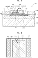
- FIG. 5 is a cross-sectional view schematically showing a structure of a normally-off HEMT 300 according to an example.
- the same reference numerals are used for substantially the same components as those in the normally-off HEMT 100 of FIG. 1 , and their detailed description is omitted.
- a depletion-forming layer 340 may be formed on the channel supply layer 130.
- the depletion-forming layer 340 includes a first part 341 having the first thickness T1, a second part 342 having the second thickness T2, and a third part 343 having the second thickness T2.
- the first part 341 may have a strip shape, and the second part 342 and third part 343 may be formed long at both sides of the first part 341 in a lengthy direction of the first part 341.
- examples are not limited thereto, and the depletion-forming layer 340 may be formed in various shapes.
- the second part 342 may be formed to be apart from the source electrode 161 and the third part 343 may be formed to be apart from the drain electrode 162. However, examples are not limited thereto.
- the second part 342 may expand as in the second part 242 of FIG. 4 and may be formed to contact the source electrode 161 and the third part 343 may expand as in the third part 243 in FIG. 4 and contact the drain electrode 162.
- the first part 341 may be formed to be closer to the source electrode 161 than the drain electrode 162.
- the depletion-forming layer 340 may function to form a depletion region in the 2DEG.
- An energy bandgap of a portion of the channel supply layer 130, which is located below the depletion-forming layer 340, may increase due to the depletion-forming layer 340, resulting in forming the depletion region of the 2DEG at a portion of the channel layer 120 corresponding to the depletion-forming layer 340.
- the 2DEG may be cut off at a portion corresponding to the first part 341 of the depletion-forming layer 340, and electron density of the 2DEG may decrease at a portion corresponding to the second part 342 and the third part 343 of the depletion-forming layer 340.
- FIG. 5 shows that a region of the 2DEG having relatively high electron density is discriminated from a region of the 2DEG having relatively low electron density by the thicknesses of dots. Electron density is high as dots are thick. A region in which the 2DEG is cut off may be a 'cut-off region', and the normally-off HEMT 300 may have a normally-off characteristic due to the cut-off region.
- the depletion-forming layer 340 may include a p-type semiconductor material. That is, the depletion-forming layer 340 may be a p-type semiconductor layer or a semiconductor layer doped with p-type impurities. In addition, the depletion-forming layer 340 may be formed of a group III-V nitride semiconductor. For example, the depletion-forming layer 340 may be formed of GaN, AIGaN, InN, AlInN, InGaN, or AlInGaN or doped with p-type impurities such as Mg. In detail, the depletion-forming layer 340 may be a p-GaN layer or a p-AIGaN layer. The depletion-forming layer 340 may cause an energy bandgap of a portion of the channel supply layer 130 therebelow to increase, thereby forming a cut-off region of the 2DEG or a region having relatively low electron density.
- a first gate electrode 371 is formed on the depletion-forming layer 340.
- the first gate electrode 371 may be formed mainly on the first part 341.
- An insulation layer 350 may be formed on the first gate electrode 371.
- the insulation layer 350 may be referred to a gate insulation layer 350 hereinafter.
- the gate insulation layer 350 may be formed to cover the depletion-forming layer 340 and the channel supply layer 130.
- the gate insulation layer 350 may be formed to have the thickness of about 50 nm to about 300 nm.
- the gate insulation layer 350 may include at least one among Al 2 O 3 , SiO x , Si x N y , Sc 2 O 3 , AIN, Ga 2 O 3 , Gd 2 O 3 , Al x Ga 2(1-x) O 3 , Al x Ga 2(1-x) O 3 , MgO, and a combination thereof.
- example embodiments are not limited thereto.
- a second gate electrode 372 is formed on the gate insulation layer 250.
- the second gate electrode 372 may be arranged above the depletion-forming layer 340.
- the first gate electrode 371 and the second gate electrode 372 may be formed of any of various metal materials and metal compounds.
- the first gate electrode 371 and the second gate electrode 372 may be formed of titanium nitride (TiN), tungsten (W), platinum (Pt), or tungsten nitride (WN) or formed in a multi-layer structure of W/Ti/AI/Ti/TiN.
- the first gate electrode 371 may be formed to have the thickness of about 100 nm to about 300 nm.
- the first gate electrode 371 and the second gate electrode 372 may be electrically connected to each other by a wire 375.
- FIG. 6 is a top view showing an electrical connection between the first gate electrode 371 and the second gate electrode 372. For convenience of description, some components are not shown in FIG. 6 .
- the second gate electrode 372 is formed on the first gate electrode 371, and the first gate electrode 371 is formed to be exposed by the second gate electrode 372.
- the wire 375 connects the exposed first gate electrode 371 to the second gate electrode 372.
- first gate electrode 371 and the second gate electrode 372 are connected to each other by the wire 375 in FIG. 6 , examples are not limited thereto.
- the second gate electrode 372 may be formed to directly contact the exposed first gate electrode 371.
- first gate electrode 371 and the second gate electrode 372 may be electrically connected to each other through an opening (refer to 152 in FIG. 1 ) formed on the gate insulation layer 350.
- FIGS. 5-6 illustrate the depletion-forming layer 340 is spaced apart from the source 161 and drain electrodes 162, examples are not limited thereto.
- the depletion-forming layer 340 of the HEMT 300 in FIGS. 5-6 may be connected to at least one of the source 161 and drain electrodes 162, similar to the HEMT 200, according to an example illustrated in FIG. 4 .
- FIGS. 5-6 illustrate the depletion forming layer 340 includes a second part 342 and a third part 343 that both have the second thickness T2, examples are not limited thereto.
- the second part 342 and the third part 343 may have different thicknesses from each other.
- Normally-off HEMTs may reduce (and/or prevent) a current from leaking in an OFF state and may decrease a turn-on resistance.
- the expansion of a depletion-forming layer causes an electric field to be dispersed, and accordingly, a breakdown voltage of a normally-off HEMT increases.
- Example embodiments described herein should be considered in a descriptive sense only and not for purposes of limitation. Descriptions of features or aspects within each HEMT according to example embodiments should typically be considered as available for other similar features or aspects in other HEMTs according to example embodiments.
Landscapes
- Junction Field-Effect Transistors (AREA)
- Insulated Gate Type Field-Effect Transistor (AREA)
Claims (6)
- Transistor à haute mobilité d'électrons normalement bloqué, HEMT, (100) comprenant :une couche de canaux (120) incluant un premier semi-conducteur nitrure ;une couche d'alimentation de canaux (130) sur la couche de canaux,la couche d'alimentation de canaux incluant un deuxième semi-conducteur nitrure,la couche d'alimentation de canaux étant configurée pour induire un gaz d'électrons bidimensionnel, 2DEG, dans la couche de canaux ;une électrode de source (161) et une électrode de drain (162) au niveau de côtés de la couche d'alimentation de canaux ;une couche de formation d'appauvrissement (140) sur la couche d'alimentation de canaux,
la couche de formation d'appauvrissement étant configurée pour former une région d'appauvrissement dans au moins une région partielle du 2DEG, la couche de formation d'appauvrissement ayant au moins deux épaisseurs ;une couche d'isolation de grille (150) sur la couche de formation d'appauvrissement, la couche d'isolation de grille définissant une ouverture qui expose une portion de la couche de formation d'appauvrissement ; etune électrode de grille (170) sur la couche d'isolation de grille, l'électrode de grille contactant la couche de formation d'appauvrissement au travers de l'ouverture, etla couche de formation d'appauvrissement incluant une première partie (141) ayant une première épaisseur, et la couche de formation d'appauvrissement incluant une deuxième partie (142) au niveau d'un côté de la première partie etla couche de formation d'appauvrissement incluant une troisième partie (143) au niveau d'un côté différent de la première partie, etl'ouverture dans la couche d'isolation de grille étant sur la première partie de la couche de formation d'appauvrissement, et la première partie de la couche de formation d'appauvrissement étant configurée pour former la région d'appauvrissement en dessous de la première partie ;la deuxième partie et la troisième partie ayant des deuxièmes épaisseurs, la première épaisseur étant plus grande que les deuxièmes épaisseurs et la deuxième partie et la troisième partie étant espacées respectivement de l'électrode de source et de l'électrode de drain, etla surface de fond de l'ensemble de la couche de formation d'appauvrissement étant plane, la première partie de la couche de formation d'appauvrissement ayant la plus grande épaisseur parmi toutes les parties de la couche de formation d'appauvrissement et étant formée au niveau de la partie centrale de la couche de formation d'appauvrissement, et les parties restantes de la couche de formation d'appauvrissement ayant des épaisseurs séquentiellement plus petites, etune densité d'électrons du 2DEG en dessous de ladite au moins une partie parmi la deuxième partie et la troisième partie de la couche de formation d'appauvrissement étant relativement plus faible qu'une densité d'électrons du 2DEG qui n'est pas situé en dessous de la couche de formation d'appauvrissement, et l'électrode de grille étant sur la couche d'isolation de grille au-dessus d'au moins une portion de chacune des première à troisième parties de la couche de formation d'appauvrissement. - HEMT normalement bloqué de la revendication 1, dans lequel
la première partie de la couche de formation d'appauvrissement est une forme de bande,
la deuxième partie et la troisième partie de la couche de formation d'appauvrissement sont des formes de bande respectives en parallèle à la première partie. - HEMT normalement bloqué de l'une quelconque des revendications précédentes, dans lequel le premier semi-conducteur nitrure inclut un matériau de nitrure de gallium (GaN).
- HEMT normalement bloqué de l'une quelconque des revendications précédentes, dans lequel le deuxième semi-conducteur nitrure inclut un nitrure incluant au moins un élément parmi l'aluminium (Al), le gallium (Ga), l'indium (In) et le bore (B).
- HEMT normalement bloqué de l'une quelconque des revendications précédentes, dans lequel la couche formant un appauvrissement inclut un semi-conducteur nitrure de type p, de préférence un matériau semi-conducteur nitrure de groupe III.
- HEMT normalement bloqué de l'une quelconque des revendications précédentes, dans lequel la première partie de la couche de formation d'appauvrissement sépare l'électrode de grille et la couche d'alimentation de canaux par une plus grande distance que la deuxième partie de la couche de formation d'appauvrissement sépare l'électrode de grille et la couche d'alimentation de canaux.
Applications Claiming Priority (1)
| Application Number | Priority Date | Filing Date | Title |
|---|---|---|---|
| KR1020120109267A KR101922122B1 (ko) | 2012-09-28 | 2012-09-28 | 노멀리 오프 고전자이동도 트랜지스터 |
Publications (3)
| Publication Number | Publication Date |
|---|---|
| EP2713402A2 EP2713402A2 (fr) | 2014-04-02 |
| EP2713402A3 EP2713402A3 (fr) | 2016-01-13 |
| EP2713402B1 true EP2713402B1 (fr) | 2021-03-24 |
Family
ID=48656003
Family Applications (1)
| Application Number | Title | Priority Date | Filing Date |
|---|---|---|---|
| EP13173455.0A Active EP2713402B1 (fr) | 2012-09-28 | 2013-06-24 | Transistor à haute mobilité d'électrons normalement bloqué |
Country Status (5)
| Country | Link |
|---|---|
| US (1) | US8890212B2 (fr) |
| EP (1) | EP2713402B1 (fr) |
| JP (1) | JP6367533B2 (fr) |
| KR (1) | KR101922122B1 (fr) |
| CN (1) | CN103715240A (fr) |
Families Citing this family (23)
| Publication number | Priority date | Publication date | Assignee | Title |
|---|---|---|---|---|
| US10700201B2 (en) * | 2012-05-23 | 2020-06-30 | Hrl Laboratories, Llc | HEMT GaN device with a non-uniform lateral two dimensional electron gas profile and method of manufacturing the same |
| CN104377241B (zh) * | 2014-09-30 | 2017-05-03 | 苏州捷芯威半导体有限公司 | 功率半导体器件及其制造方法 |
| JP6646363B2 (ja) * | 2015-06-02 | 2020-02-14 | 株式会社アドバンテスト | 半導体装置 |
| WO2017069462A1 (fr) * | 2015-10-23 | 2017-04-27 | (주)기가레인 | Transistor à haute mobilité d'électrons et son procédé de fabrication |
| CN105810728B (zh) * | 2016-05-06 | 2019-06-18 | 西安电子科技大学 | 增强型鳍式绝缘栅高电子迁移率晶体管 |
| DE102017210711A1 (de) | 2016-06-27 | 2017-12-28 | Fraunhofer-Gesellschaft zur Förderung der angewandten Forschung e.V. | Halbleiterbauelement |
| US10211328B2 (en) | 2016-09-20 | 2019-02-19 | Board Of Trustees Of The University Of Illinois | Normally-off cubic phase GaN (c-GaN) HEMT having a gate electrode dielectrically insulated from a c-AlGaN capping layer |
| CN106876443A (zh) * | 2017-03-03 | 2017-06-20 | 上海新傲科技股份有限公司 | 高击穿电压的氮化镓高电子迁移率晶体管及其形成方法 |
| CN111183523A (zh) * | 2018-01-12 | 2020-05-19 | 英特尔公司 | 在源极区和漏极区之间包括第一和第二半导体材料的晶体管及其制造方法 |
| JP7175727B2 (ja) * | 2018-11-30 | 2022-11-21 | ローム株式会社 | 窒化物半導体装置 |
| EP3719850A1 (fr) * | 2019-04-03 | 2020-10-07 | Infineon Technologies Austria AG | Transistor à base de nitrures d'éléments iii et méthode de fabrication d'une structure de grille pour un transistor à base de nitrures d'éléments iii |
| US12550356B2 (en) | 2019-04-15 | 2026-02-10 | Rohm Co. Ltd. | Nitride semiconductor device and method for manufacturing same |
| KR102257205B1 (ko) * | 2019-11-29 | 2021-05-27 | 주식회사 시지트로닉스 | 전계 완화를 위한 질화물 반도체 소자 및 그 제조 방법 |
| KR102767849B1 (ko) * | 2019-12-12 | 2025-02-14 | 삼성전자주식회사 | 반도체 장치 및 그 제조 방법 |
| JP7258735B2 (ja) | 2019-12-13 | 2023-04-17 | 株式会社東芝 | 半導体装置 |
| CN111682066A (zh) * | 2020-06-19 | 2020-09-18 | 英诺赛科(珠海)科技有限公司 | 具有改善栅极漏电流的半导体器件 |
| KR102792554B1 (ko) * | 2020-06-23 | 2025-04-08 | 삼성전자주식회사 | 고 전자 이동도 트랜지스터 및 그 제조방법 |
| TWI768391B (zh) * | 2020-07-02 | 2022-06-21 | 聯華電子股份有限公司 | 高電子遷移率電晶體的佈局圖 |
| FR3115156B1 (fr) * | 2020-10-09 | 2022-08-26 | Commissariat Energie Atomique | Transistor à nitrure de gallium |
| WO2022113536A1 (fr) * | 2020-11-26 | 2022-06-02 | ローム株式会社 | Dispositif à semi-conducteur au nitrure et son procédé de fabrication |
| US11942326B2 (en) * | 2020-12-16 | 2024-03-26 | Semiconductor Components Industries, Llc | Process of forming an electronic device including a doped gate electrode |
| KR102547803B1 (ko) * | 2021-05-18 | 2023-06-26 | 삼성전자주식회사 | 고 전자 이동도 트랜지스터 |
| JP7524140B2 (ja) * | 2021-07-26 | 2024-07-29 | 株式会社東芝 | 半導体装置 |
Citations (1)
| Publication number | Priority date | Publication date | Assignee | Title |
|---|---|---|---|---|
| WO2011163318A2 (fr) * | 2010-06-23 | 2011-12-29 | Cornell University | Structure semi-conductrice iii-v à grille et procédé |
Family Cites Families (23)
| Publication number | Priority date | Publication date | Assignee | Title |
|---|---|---|---|---|
| US6548333B2 (en) | 2000-12-01 | 2003-04-15 | Cree, Inc. | Aluminum gallium nitride/gallium nitride high electron mobility transistors having a gate contact on a gallium nitride based cap segment |
| JP2002231821A (ja) | 2001-01-31 | 2002-08-16 | Mitsubishi Electric Corp | 半導体装置の製造方法及び半導体装置 |
| JP5000057B2 (ja) | 2001-07-17 | 2012-08-15 | ルネサスエレクトロニクス株式会社 | 半導体装置及びその製造方法 |
| JP2005175143A (ja) | 2003-12-10 | 2005-06-30 | Matsushita Electric Ind Co Ltd | 半導体装置およびその製造方法 |
| JP4041075B2 (ja) | 2004-02-27 | 2008-01-30 | 株式会社東芝 | 半導体装置 |
| JP4700295B2 (ja) | 2004-06-08 | 2011-06-15 | 富士通セミコンダクター株式会社 | 半導体装置とその製造方法 |
| US7129127B2 (en) | 2004-09-24 | 2006-10-31 | Texas Instruments Incorporated | Integration scheme to improve NMOS with poly cap while mitigating PMOS degradation |
| JP4705412B2 (ja) | 2005-06-06 | 2011-06-22 | パナソニック株式会社 | 電界効果トランジスタ及びその製造方法 |
| US20090173968A1 (en) * | 2005-12-14 | 2009-07-09 | Nec Corporation | Field Effect Transistor |
| JP4755961B2 (ja) * | 2006-09-29 | 2011-08-24 | パナソニック株式会社 | 窒化物半導体装置及びその製造方法 |
| CN101523614B (zh) * | 2006-11-20 | 2011-04-20 | 松下电器产业株式会社 | 半导体装置及其驱动方法 |
| JP4712683B2 (ja) * | 2006-12-21 | 2011-06-29 | パナソニック株式会社 | トランジスタおよびその製造方法 |
| JP5114947B2 (ja) | 2006-12-28 | 2013-01-09 | 富士通株式会社 | 窒化物半導体装置とその製造方法 |
| US7872305B2 (en) | 2008-06-26 | 2011-01-18 | Fairchild Semiconductor Corporation | Shielded gate trench FET with an inter-electrode dielectric having a nitride layer therein |
| US7985986B2 (en) | 2008-07-31 | 2011-07-26 | Cree, Inc. | Normally-off semiconductor devices |
| JP5468768B2 (ja) | 2008-12-05 | 2014-04-09 | パナソニック株式会社 | 電界効果トランジスタ及びその製造方法 |
| DE112010001589B4 (de) | 2009-04-08 | 2024-11-28 | Efficient Power Conversion Corporation | Kompensierter GATE-MISFET |
| US20110210377A1 (en) * | 2010-02-26 | 2011-09-01 | Infineon Technologies Austria Ag | Nitride semiconductor device |
| JP2011204877A (ja) * | 2010-03-25 | 2011-10-13 | Panasonic Corp | 電界効果トランジスタ及びその評価方法 |
| JP5649112B2 (ja) * | 2010-07-30 | 2015-01-07 | パナソニック株式会社 | 電界効果トランジスタ |
| JP5620767B2 (ja) | 2010-09-17 | 2014-11-05 | パナソニック株式会社 | 半導体装置 |
| KR102065115B1 (ko) * | 2010-11-05 | 2020-01-13 | 삼성전자주식회사 | E-모드를 갖는 고 전자 이동도 트랜지스터 및 그 제조방법 |
| JP4815020B2 (ja) | 2011-02-02 | 2011-11-16 | パナソニック株式会社 | 窒化物半導体装置 |
-
2012
- 2012-09-28 KR KR1020120109267A patent/KR101922122B1/ko active Active
-
2013
- 2013-04-15 CN CN201310128726.9A patent/CN103715240A/zh active Pending
- 2013-05-01 US US13/874,920 patent/US8890212B2/en active Active
- 2013-06-24 EP EP13173455.0A patent/EP2713402B1/fr active Active
- 2013-09-26 JP JP2013199373A patent/JP6367533B2/ja active Active
Patent Citations (1)
| Publication number | Priority date | Publication date | Assignee | Title |
|---|---|---|---|---|
| WO2011163318A2 (fr) * | 2010-06-23 | 2011-12-29 | Cornell University | Structure semi-conductrice iii-v à grille et procédé |
Also Published As
| Publication number | Publication date |
|---|---|
| EP2713402A2 (fr) | 2014-04-02 |
| KR101922122B1 (ko) | 2018-11-26 |
| US20140091363A1 (en) | 2014-04-03 |
| EP2713402A3 (fr) | 2016-01-13 |
| KR20140042470A (ko) | 2014-04-07 |
| CN103715240A (zh) | 2014-04-09 |
| JP2014072528A (ja) | 2014-04-21 |
| JP6367533B2 (ja) | 2018-08-01 |
| US8890212B2 (en) | 2014-11-18 |
Similar Documents
| Publication | Publication Date | Title |
|---|---|---|
| EP2713402B1 (fr) | Transistor à haute mobilité d'électrons normalement bloqué | |
| EP2720272B1 (fr) | Transistor à haute mobilité d'électrons et sa méthode d'opération | |
| KR101927408B1 (ko) | 고전자 이동도 트랜지스터 및 그 제조방법 | |
| US9129889B2 (en) | High electron mobility semiconductor device and method therefor | |
| US9147738B2 (en) | High electron mobility transistor including plurality of gate electrodes | |
| EP2722890B1 (fr) | Structure de diode de schottky et procédé de fabrication | |
| US9245738B2 (en) | High electron mobility transistor and method of manufacturing the same | |
| KR101922120B1 (ko) | 고전자이동도 트랜지스터 및 그 제조방법 | |
| US8860089B2 (en) | High electron mobility transistor and method of manufacturing the same | |
| CN101689564B (zh) | 异质结构场效应晶体管及其制造方法和集成电路 | |
| CN102623498A (zh) | 半导体元件 | |
| KR20150065005A (ko) | 노멀리 오프 고전자이동도 트랜지스터 | |
| CN104704615A (zh) | 开关元件 | |
| US12002879B2 (en) | High electron mobility transistor and method of manufacturing the same | |
| US9570597B2 (en) | High electron mobility transistor | |
| KR102038618B1 (ko) | 고전자이동도 트랜지스터 | |
| KR101887535B1 (ko) | 고전자 이동도 트랜지스터 및 그 제조방법 | |
| KR20150044325A (ko) | 고전자 이동도 트랜지스터를 포함하는 전자 장치 |
Legal Events
| Date | Code | Title | Description |
|---|---|---|---|
| PUAI | Public reference made under article 153(3) epc to a published international application that has entered the european phase |
Free format text: ORIGINAL CODE: 0009012 |
|
| AK | Designated contracting states |
Kind code of ref document: A2 Designated state(s): AL AT BE BG CH CY CZ DE DK EE ES FI FR GB GR HR HU IE IS IT LI LT LU LV MC MK MT NL NO PL PT RO RS SE SI SK SM TR |
|
| AX | Request for extension of the european patent |
Extension state: BA ME |
|
| PUAL | Search report despatched |
Free format text: ORIGINAL CODE: 0009013 |
|
| AK | Designated contracting states |
Kind code of ref document: A3 Designated state(s): AL AT BE BG CH CY CZ DE DK EE ES FI FR GB GR HR HU IE IS IT LI LT LU LV MC MK MT NL NO PL PT RO RS SE SI SK SM TR |
|
| AX | Request for extension of the european patent |
Extension state: BA ME |
|
| RIC1 | Information provided on ipc code assigned before grant |
Ipc: H01L 29/778 20060101AFI20151207BHEP Ipc: H01L 29/20 20060101ALN20151207BHEP Ipc: H01L 29/10 20060101ALI20151207BHEP Ipc: H01L 29/40 20060101ALN20151207BHEP Ipc: H01L 29/423 20060101ALN20151207BHEP |
|
| 17P | Request for examination filed |
Effective date: 20160707 |
|
| RBV | Designated contracting states (corrected) |
Designated state(s): AL AT BE BG CH CY CZ DE DK EE ES FI FR GB GR HR HU IE IS IT LI LT LU LV MC MK MT NL NO PL PT RO RS SE SI SK SM TR |
|
| STAA | Information on the status of an ep patent application or granted ep patent |
Free format text: STATUS: EXAMINATION IS IN PROGRESS |
|
| 17Q | First examination report despatched |
Effective date: 20170320 |
|
| GRAP | Despatch of communication of intention to grant a patent |
Free format text: ORIGINAL CODE: EPIDOSNIGR1 |
|
| STAA | Information on the status of an ep patent application or granted ep patent |
Free format text: STATUS: GRANT OF PATENT IS INTENDED |
|
| RIC1 | Information provided on ipc code assigned before grant |
Ipc: H01L 29/778 20060101AFI20200916BHEP Ipc: H01L 29/10 20060101ALI20200916BHEP Ipc: H01L 29/20 20060101ALN20200916BHEP Ipc: H01L 29/423 20060101ALN20200916BHEP Ipc: H01L 29/40 20060101ALN20200916BHEP |
|
| RIC1 | Information provided on ipc code assigned before grant |
Ipc: H01L 29/20 20060101ALN20200921BHEP Ipc: H01L 29/778 20060101AFI20200921BHEP Ipc: H01L 29/40 20060101ALN20200921BHEP Ipc: H01L 29/423 20060101ALN20200921BHEP Ipc: H01L 29/10 20060101ALI20200921BHEP |
|
| INTG | Intention to grant announced |
Effective date: 20201008 |
|
| GRAS | Grant fee paid |
Free format text: ORIGINAL CODE: EPIDOSNIGR3 |
|
| GRAA | (expected) grant |
Free format text: ORIGINAL CODE: 0009210 |
|
| STAA | Information on the status of an ep patent application or granted ep patent |
Free format text: STATUS: THE PATENT HAS BEEN GRANTED |
|
| AK | Designated contracting states |
Kind code of ref document: B1 Designated state(s): AL AT BE BG CH CY CZ DE DK EE ES FI FR GB GR HR HU IE IS IT LI LT LU LV MC MK MT NL NO PL PT RO RS SE SI SK SM TR |
|
| REG | Reference to a national code |
Ref country code: GB Ref legal event code: FG4D |
|
| REG | Reference to a national code |
Ref country code: CH Ref legal event code: EP |
|
| REG | Reference to a national code |
Ref country code: DE Ref legal event code: R096 Ref document number: 602013076408 Country of ref document: DE |
|
| REG | Reference to a national code |
Ref country code: IE Ref legal event code: FG4D |
|
| REG | Reference to a national code |
Ref country code: AT Ref legal event code: REF Ref document number: 1375381 Country of ref document: AT Kind code of ref document: T Effective date: 20210415 |
|
| REG | Reference to a national code |
Ref country code: LT Ref legal event code: MG9D |
|
| PG25 | Lapsed in a contracting state [announced via postgrant information from national office to epo] |
Ref country code: HR Free format text: LAPSE BECAUSE OF FAILURE TO SUBMIT A TRANSLATION OF THE DESCRIPTION OR TO PAY THE FEE WITHIN THE PRESCRIBED TIME-LIMIT Effective date: 20210324 Ref country code: FI Free format text: LAPSE BECAUSE OF FAILURE TO SUBMIT A TRANSLATION OF THE DESCRIPTION OR TO PAY THE FEE WITHIN THE PRESCRIBED TIME-LIMIT Effective date: 20210324 Ref country code: GR Free format text: LAPSE BECAUSE OF FAILURE TO SUBMIT A TRANSLATION OF THE DESCRIPTION OR TO PAY THE FEE WITHIN THE PRESCRIBED TIME-LIMIT Effective date: 20210625 Ref country code: BG Free format text: LAPSE BECAUSE OF FAILURE TO SUBMIT A TRANSLATION OF THE DESCRIPTION OR TO PAY THE FEE WITHIN THE PRESCRIBED TIME-LIMIT Effective date: 20210624 Ref country code: NO Free format text: LAPSE BECAUSE OF FAILURE TO SUBMIT A TRANSLATION OF THE DESCRIPTION OR TO PAY THE FEE WITHIN THE PRESCRIBED TIME-LIMIT Effective date: 20210624 |
|
| PG25 | Lapsed in a contracting state [announced via postgrant information from national office to epo] |
Ref country code: RS Free format text: LAPSE BECAUSE OF FAILURE TO SUBMIT A TRANSLATION OF THE DESCRIPTION OR TO PAY THE FEE WITHIN THE PRESCRIBED TIME-LIMIT Effective date: 20210324 Ref country code: LV Free format text: LAPSE BECAUSE OF FAILURE TO SUBMIT A TRANSLATION OF THE DESCRIPTION OR TO PAY THE FEE WITHIN THE PRESCRIBED TIME-LIMIT Effective date: 20210324 Ref country code: SE Free format text: LAPSE BECAUSE OF FAILURE TO SUBMIT A TRANSLATION OF THE DESCRIPTION OR TO PAY THE FEE WITHIN THE PRESCRIBED TIME-LIMIT Effective date: 20210324 |
|
| REG | Reference to a national code |
Ref country code: NL Ref legal event code: MP Effective date: 20210324 |
|
| REG | Reference to a national code |
Ref country code: AT Ref legal event code: MK05 Ref document number: 1375381 Country of ref document: AT Kind code of ref document: T Effective date: 20210324 |
|
| PG25 | Lapsed in a contracting state [announced via postgrant information from national office to epo] |
Ref country code: NL Free format text: LAPSE BECAUSE OF FAILURE TO SUBMIT A TRANSLATION OF THE DESCRIPTION OR TO PAY THE FEE WITHIN THE PRESCRIBED TIME-LIMIT Effective date: 20210324 |
|
| PG25 | Lapsed in a contracting state [announced via postgrant information from national office to epo] |
Ref country code: LT Free format text: LAPSE BECAUSE OF FAILURE TO SUBMIT A TRANSLATION OF THE DESCRIPTION OR TO PAY THE FEE WITHIN THE PRESCRIBED TIME-LIMIT Effective date: 20210324 Ref country code: CZ Free format text: LAPSE BECAUSE OF FAILURE TO SUBMIT A TRANSLATION OF THE DESCRIPTION OR TO PAY THE FEE WITHIN THE PRESCRIBED TIME-LIMIT Effective date: 20210324 Ref country code: EE Free format text: LAPSE BECAUSE OF FAILURE TO SUBMIT A TRANSLATION OF THE DESCRIPTION OR TO PAY THE FEE WITHIN THE PRESCRIBED TIME-LIMIT Effective date: 20210324 Ref country code: SM Free format text: LAPSE BECAUSE OF FAILURE TO SUBMIT A TRANSLATION OF THE DESCRIPTION OR TO PAY THE FEE WITHIN THE PRESCRIBED TIME-LIMIT Effective date: 20210324 Ref country code: AT Free format text: LAPSE BECAUSE OF FAILURE TO SUBMIT A TRANSLATION OF THE DESCRIPTION OR TO PAY THE FEE WITHIN THE PRESCRIBED TIME-LIMIT Effective date: 20210324 |
|
| PG25 | Lapsed in a contracting state [announced via postgrant information from national office to epo] |
Ref country code: PT Free format text: LAPSE BECAUSE OF FAILURE TO SUBMIT A TRANSLATION OF THE DESCRIPTION OR TO PAY THE FEE WITHIN THE PRESCRIBED TIME-LIMIT Effective date: 20210726 Ref country code: PL Free format text: LAPSE BECAUSE OF FAILURE TO SUBMIT A TRANSLATION OF THE DESCRIPTION OR TO PAY THE FEE WITHIN THE PRESCRIBED TIME-LIMIT Effective date: 20210324 Ref country code: ES Free format text: LAPSE BECAUSE OF FAILURE TO SUBMIT A TRANSLATION OF THE DESCRIPTION OR TO PAY THE FEE WITHIN THE PRESCRIBED TIME-LIMIT Effective date: 20210324 Ref country code: SK Free format text: LAPSE BECAUSE OF FAILURE TO SUBMIT A TRANSLATION OF THE DESCRIPTION OR TO PAY THE FEE WITHIN THE PRESCRIBED TIME-LIMIT Effective date: 20210324 Ref country code: RO Free format text: LAPSE BECAUSE OF FAILURE TO SUBMIT A TRANSLATION OF THE DESCRIPTION OR TO PAY THE FEE WITHIN THE PRESCRIBED TIME-LIMIT Effective date: 20210324 Ref country code: IS Free format text: LAPSE BECAUSE OF FAILURE TO SUBMIT A TRANSLATION OF THE DESCRIPTION OR TO PAY THE FEE WITHIN THE PRESCRIBED TIME-LIMIT Effective date: 20210724 |
|
| REG | Reference to a national code |
Ref country code: DE Ref legal event code: R097 Ref document number: 602013076408 Country of ref document: DE |
|
| PG25 | Lapsed in a contracting state [announced via postgrant information from national office to epo] |
Ref country code: AL Free format text: LAPSE BECAUSE OF FAILURE TO SUBMIT A TRANSLATION OF THE DESCRIPTION OR TO PAY THE FEE WITHIN THE PRESCRIBED TIME-LIMIT Effective date: 20210324 Ref country code: MC Free format text: LAPSE BECAUSE OF FAILURE TO SUBMIT A TRANSLATION OF THE DESCRIPTION OR TO PAY THE FEE WITHIN THE PRESCRIBED TIME-LIMIT Effective date: 20210324 Ref country code: DK Free format text: LAPSE BECAUSE OF FAILURE TO SUBMIT A TRANSLATION OF THE DESCRIPTION OR TO PAY THE FEE WITHIN THE PRESCRIBED TIME-LIMIT Effective date: 20210324 |
|
| REG | Reference to a national code |
Ref country code: CH Ref legal event code: PL |
|
| PLBE | No opposition filed within time limit |
Free format text: ORIGINAL CODE: 0009261 |
|
| STAA | Information on the status of an ep patent application or granted ep patent |
Free format text: STATUS: NO OPPOSITION FILED WITHIN TIME LIMIT |
|
| PG25 | Lapsed in a contracting state [announced via postgrant information from national office to epo] |
Ref country code: SI Free format text: LAPSE BECAUSE OF FAILURE TO SUBMIT A TRANSLATION OF THE DESCRIPTION OR TO PAY THE FEE WITHIN THE PRESCRIBED TIME-LIMIT Effective date: 20210324 |
|
| 26N | No opposition filed |
Effective date: 20220104 |
|
| REG | Reference to a national code |
Ref country code: BE Ref legal event code: MM Effective date: 20210630 |
|
| PG25 | Lapsed in a contracting state [announced via postgrant information from national office to epo] |
Ref country code: LU Free format text: LAPSE BECAUSE OF NON-PAYMENT OF DUE FEES Effective date: 20210624 |
|
| PG25 | Lapsed in a contracting state [announced via postgrant information from national office to epo] |
Ref country code: LI Free format text: LAPSE BECAUSE OF NON-PAYMENT OF DUE FEES Effective date: 20210630 Ref country code: IE Free format text: LAPSE BECAUSE OF NON-PAYMENT OF DUE FEES Effective date: 20210624 Ref country code: CH Free format text: LAPSE BECAUSE OF NON-PAYMENT OF DUE FEES Effective date: 20210630 |
|
| PG25 | Lapsed in a contracting state [announced via postgrant information from national office to epo] |
Ref country code: IS Free format text: LAPSE BECAUSE OF FAILURE TO SUBMIT A TRANSLATION OF THE DESCRIPTION OR TO PAY THE FEE WITHIN THE PRESCRIBED TIME-LIMIT Effective date: 20210724 |
|
| PG25 | Lapsed in a contracting state [announced via postgrant information from national office to epo] |
Ref country code: BE Free format text: LAPSE BECAUSE OF NON-PAYMENT OF DUE FEES Effective date: 20210630 |
|
| PG25 | Lapsed in a contracting state [announced via postgrant information from national office to epo] |
Ref country code: IT Free format text: LAPSE BECAUSE OF FAILURE TO SUBMIT A TRANSLATION OF THE DESCRIPTION OR TO PAY THE FEE WITHIN THE PRESCRIBED TIME-LIMIT Effective date: 20210324 |
|
| PG25 | Lapsed in a contracting state [announced via postgrant information from national office to epo] |
Ref country code: HU Free format text: LAPSE BECAUSE OF FAILURE TO SUBMIT A TRANSLATION OF THE DESCRIPTION OR TO PAY THE FEE WITHIN THE PRESCRIBED TIME-LIMIT; INVALID AB INITIO Effective date: 20130624 |
|
| PG25 | Lapsed in a contracting state [announced via postgrant information from national office to epo] |
Ref country code: CY Free format text: LAPSE BECAUSE OF FAILURE TO SUBMIT A TRANSLATION OF THE DESCRIPTION OR TO PAY THE FEE WITHIN THE PRESCRIBED TIME-LIMIT Effective date: 20210324 |
|
| P01 | Opt-out of the competence of the unified patent court (upc) registered |
Effective date: 20230530 |
|
| PG25 | Lapsed in a contracting state [announced via postgrant information from national office to epo] |
Ref country code: MK Free format text: LAPSE BECAUSE OF FAILURE TO SUBMIT A TRANSLATION OF THE DESCRIPTION OR TO PAY THE FEE WITHIN THE PRESCRIBED TIME-LIMIT Effective date: 20210324 |
|
| PG25 | Lapsed in a contracting state [announced via postgrant information from national office to epo] |
Ref country code: MT Free format text: LAPSE BECAUSE OF FAILURE TO SUBMIT A TRANSLATION OF THE DESCRIPTION OR TO PAY THE FEE WITHIN THE PRESCRIBED TIME-LIMIT Effective date: 20210324 |
|
| REG | Reference to a national code |
Ref country code: DE Ref legal event code: R079 Ref document number: 602013076408 Country of ref document: DE Free format text: PREVIOUS MAIN CLASS: H01L0029778000 Ipc: H10D0030470000 |
|
| PGFP | Annual fee paid to national office [announced via postgrant information from national office to epo] |
Ref country code: DE Payment date: 20250507 Year of fee payment: 13 |
|
| PGFP | Annual fee paid to national office [announced via postgrant information from national office to epo] |
Ref country code: GB Payment date: 20250508 Year of fee payment: 13 |
|
| PGFP | Annual fee paid to national office [announced via postgrant information from national office to epo] |
Ref country code: FR Payment date: 20250508 Year of fee payment: 13 |
|
| PG25 | Lapsed in a contracting state [announced via postgrant information from national office to epo] |
Ref country code: TR Free format text: LAPSE BECAUSE OF FAILURE TO SUBMIT A TRANSLATION OF THE DESCRIPTION OR TO PAY THE FEE WITHIN THE PRESCRIBED TIME-LIMIT Effective date: 20210324 |