EP2699966B1 - Network architecture and protocol for cluster of lithography machines - Google Patents
Network architecture and protocol for cluster of lithography machines Download PDFInfo
- Publication number
- EP2699966B1 EP2699966B1 EP12716017.4A EP12716017A EP2699966B1 EP 2699966 B1 EP2699966 B1 EP 2699966B1 EP 12716017 A EP12716017 A EP 12716017A EP 2699966 B1 EP2699966 B1 EP 2699966B1
- Authority
- EP
- European Patent Office
- Prior art keywords
- lithography
- data
- command
- subsystem
- control unit
- Prior art date
- Legal status (The legal status is an assumption and is not a legal conclusion. Google has not performed a legal analysis and makes no representation as to the accuracy of the status listed.)
- Active
Links
- 238000001459 lithography Methods 0.000 title claims description 105
- 230000008569 process Effects 0.000 claims description 33
- 230000009471 action Effects 0.000 claims description 27
- 238000004891 communication Methods 0.000 claims description 26
- 238000000034 method Methods 0.000 claims description 24
- 239000000758 substrate Substances 0.000 claims description 24
- 235000012431 wafers Nutrition 0.000 claims description 20
- 238000012545 processing Methods 0.000 claims description 18
- 230000005540 biological transmission Effects 0.000 claims description 16
- 230000004044 response Effects 0.000 claims description 7
- 230000000977 initiatory effect Effects 0.000 claims 1
- 238000010586 diagram Methods 0.000 description 18
- 230000006870 function Effects 0.000 description 13
- 239000002245 particle Substances 0.000 description 12
- 230000006399 behavior Effects 0.000 description 8
- 238000013461 design Methods 0.000 description 8
- 238000012546 transfer Methods 0.000 description 8
- 238000013480 data collection Methods 0.000 description 6
- 238000012384 transportation and delivery Methods 0.000 description 6
- 238000005259 measurement Methods 0.000 description 5
- 238000000926 separation method Methods 0.000 description 5
- 230000002269 spontaneous effect Effects 0.000 description 4
- 238000003491 array Methods 0.000 description 3
- 238000013523 data management Methods 0.000 description 3
- 238000013500 data storage Methods 0.000 description 3
- 238000004519 manufacturing process Methods 0.000 description 3
- 238000003860 storage Methods 0.000 description 3
- 208000036758 Postinfectious cerebellitis Diseases 0.000 description 2
- 230000001419 dependent effect Effects 0.000 description 2
- 238000011161 development Methods 0.000 description 2
- 238000010894 electron beam technology Methods 0.000 description 2
- 230000000737 periodic effect Effects 0.000 description 2
- 230000004913 activation Effects 0.000 description 1
- 230000008859 change Effects 0.000 description 1
- 238000006243 chemical reaction Methods 0.000 description 1
- 238000012790 confirmation Methods 0.000 description 1
- 230000008094 contradictory effect Effects 0.000 description 1
- 238000012937 correction Methods 0.000 description 1
- 238000013497 data interchange Methods 0.000 description 1
- 230000002950 deficient Effects 0.000 description 1
- 238000003745 diagnosis Methods 0.000 description 1
- 230000000694 effects Effects 0.000 description 1
- 230000004907 flux Effects 0.000 description 1
- 238000005286 illumination Methods 0.000 description 1
- 230000003993 interaction Effects 0.000 description 1
- 230000002452 interceptive effect Effects 0.000 description 1
- 238000007726 management method Methods 0.000 description 1
- 230000007246 mechanism Effects 0.000 description 1
- 238000012986 modification Methods 0.000 description 1
- 230000004048 modification Effects 0.000 description 1
- 235000021110 pickles Nutrition 0.000 description 1
- 238000011084 recovery Methods 0.000 description 1
- 239000004065 semiconductor Substances 0.000 description 1
- 230000001360 synchronised effect Effects 0.000 description 1
- 238000012360 testing method Methods 0.000 description 1
Images


Classifications
-
- G—PHYSICS
- G03—PHOTOGRAPHY; CINEMATOGRAPHY; ANALOGOUS TECHNIQUES USING WAVES OTHER THAN OPTICAL WAVES; ELECTROGRAPHY; HOLOGRAPHY
- G03F—PHOTOMECHANICAL PRODUCTION OF TEXTURED OR PATTERNED SURFACES, e.g. FOR PRINTING, FOR PROCESSING OF SEMICONDUCTOR DEVICES; MATERIALS THEREFOR; ORIGINALS THEREFOR; APPARATUS SPECIALLY ADAPTED THEREFOR
- G03F7/00—Photomechanical, e.g. photolithographic, production of textured or patterned surfaces, e.g. printing surfaces; Materials therefor, e.g. comprising photoresists; Apparatus specially adapted therefor
- G03F7/70—Microphotolithographic exposure; Apparatus therefor
- G03F7/70483—Information management; Active and passive control; Testing; Wafer monitoring, e.g. pattern monitoring
- G03F7/70491—Information management, e.g. software; Active and passive control, e.g. details of controlling exposure processes or exposure tool monitoring processes
- G03F7/70525—Controlling normal operating mode, e.g. matching different apparatus, remote control or prediction of failure
-
- G—PHYSICS
- G03—PHOTOGRAPHY; CINEMATOGRAPHY; ANALOGOUS TECHNIQUES USING WAVES OTHER THAN OPTICAL WAVES; ELECTROGRAPHY; HOLOGRAPHY
- G03F—PHOTOMECHANICAL PRODUCTION OF TEXTURED OR PATTERNED SURFACES, e.g. FOR PRINTING, FOR PROCESSING OF SEMICONDUCTOR DEVICES; MATERIALS THEREFOR; ORIGINALS THEREFOR; APPARATUS SPECIALLY ADAPTED THEREFOR
- G03F7/00—Photomechanical, e.g. photolithographic, production of textured or patterned surfaces, e.g. printing surfaces; Materials therefor, e.g. comprising photoresists; Apparatus specially adapted therefor
- G03F7/70—Microphotolithographic exposure; Apparatus therefor
- G03F7/70483—Information management; Active and passive control; Testing; Wafer monitoring, e.g. pattern monitoring
- G03F7/70491—Information management, e.g. software; Active and passive control, e.g. details of controlling exposure processes or exposure tool monitoring processes
- G03F7/70508—Data handling in all parts of the microlithographic apparatus, e.g. handling pattern data for addressable masks or data transfer to or from different components within the exposure apparatus
-
- G—PHYSICS
- G03—PHOTOGRAPHY; CINEMATOGRAPHY; ANALOGOUS TECHNIQUES USING WAVES OTHER THAN OPTICAL WAVES; ELECTROGRAPHY; HOLOGRAPHY
- G03F—PHOTOMECHANICAL PRODUCTION OF TEXTURED OR PATTERNED SURFACES, e.g. FOR PRINTING, FOR PROCESSING OF SEMICONDUCTOR DEVICES; MATERIALS THEREFOR; ORIGINALS THEREFOR; APPARATUS SPECIALLY ADAPTED THEREFOR
- G03F7/00—Photomechanical, e.g. photolithographic, production of textured or patterned surfaces, e.g. printing surfaces; Materials therefor, e.g. comprising photoresists; Apparatus specially adapted therefor
- G03F7/70—Microphotolithographic exposure; Apparatus therefor
- G03F7/708—Construction of apparatus, e.g. environment aspects, hygiene aspects or materials
- G03F7/70991—Connection with other apparatus, e.g. multiple exposure stations, particular arrangement of exposure apparatus and pre-exposure and/or post-exposure apparatus; Shared apparatus, e.g. having shared radiation source, shared mask or workpiece stage, shared base-plate; Utilities, e.g. cable, pipe or wireless arrangements for data, power, fluids or vacuum
-
- G—PHYSICS
- G05—CONTROLLING; REGULATING
- G05B—CONTROL OR REGULATING SYSTEMS IN GENERAL; FUNCTIONAL ELEMENTS OF SUCH SYSTEMS; MONITORING OR TESTING ARRANGEMENTS FOR SUCH SYSTEMS OR ELEMENTS
- G05B19/00—Programme-control systems
- G05B19/02—Programme-control systems electric
- G05B19/418—Total factory control, i.e. centrally controlling a plurality of machines, e.g. direct or distributed numerical control [DNC], flexible manufacturing systems [FMS], integrated manufacturing systems [IMS] or computer integrated manufacturing [CIM]
- G05B19/41865—Total factory control, i.e. centrally controlling a plurality of machines, e.g. direct or distributed numerical control [DNC], flexible manufacturing systems [FMS], integrated manufacturing systems [IMS] or computer integrated manufacturing [CIM] characterised by job scheduling, process planning, material flow
-
- G—PHYSICS
- G06—COMPUTING; CALCULATING OR COUNTING
- G06F—ELECTRIC DIGITAL DATA PROCESSING
- G06F9/00—Arrangements for program control, e.g. control units
- G06F9/06—Arrangements for program control, e.g. control units using stored programs, i.e. using an internal store of processing equipment to receive or retain programs
- G06F9/46—Multiprogramming arrangements
- G06F9/48—Program initiating; Program switching, e.g. by interrupt
-
- H—ELECTRICITY
- H01—ELECTRIC ELEMENTS
- H01J—ELECTRIC DISCHARGE TUBES OR DISCHARGE LAMPS
- H01J37/00—Discharge tubes with provision for introducing objects or material to be exposed to the discharge, e.g. for the purpose of examination or processing thereof
- H01J37/30—Electron-beam or ion-beam tubes for localised treatment of objects
- H01J37/317—Electron-beam or ion-beam tubes for localised treatment of objects for changing properties of the objects or for applying thin layers thereon, e.g. for ion implantation
- H01J37/3174—Particle-beam lithography, e.g. electron beam lithography
- H01J37/3177—Multi-beam, e.g. fly's eye, comb probe
-
- B—PERFORMING OPERATIONS; TRANSPORTING
- B82—NANOTECHNOLOGY
- B82Y—SPECIFIC USES OR APPLICATIONS OF NANOSTRUCTURES; MEASUREMENT OR ANALYSIS OF NANOSTRUCTURES; MANUFACTURE OR TREATMENT OF NANOSTRUCTURES
- B82Y10/00—Nanotechnology for information processing, storage or transmission, e.g. quantum computing or single electron logic
-
- B—PERFORMING OPERATIONS; TRANSPORTING
- B82—NANOTECHNOLOGY
- B82Y—SPECIFIC USES OR APPLICATIONS OF NANOSTRUCTURES; MEASUREMENT OR ANALYSIS OF NANOSTRUCTURES; MANUFACTURE OR TREATMENT OF NANOSTRUCTURES
- B82Y40/00—Manufacture or treatment of nanostructures
-
- G—PHYSICS
- G06—COMPUTING; CALCULATING OR COUNTING
- G06F—ELECTRIC DIGITAL DATA PROCESSING
- G06F9/00—Arrangements for program control, e.g. control units
- G06F9/06—Arrangements for program control, e.g. control units using stored programs, i.e. using an internal store of processing equipment to receive or retain programs
- G06F9/46—Multiprogramming arrangements
- G06F9/48—Program initiating; Program switching, e.g. by interrupt
- G06F9/4806—Task transfer initiation or dispatching
- G06F9/4843—Task transfer initiation or dispatching by program, e.g. task dispatcher, supervisor, operating system
- G06F9/4881—Scheduling strategies for dispatcher, e.g. round robin, multi-level priority queues
Definitions
- the invention relates to a clustered substrate processing system comprising a plurality of lithography elements each arranged for independent exposure of substrates according to pattern data, and more particularly to network architecture and protocol for such a clustered substrate processing system.
- Lithography machines have become more complex with numerous subsystems for performing various functions within the machine, and complex software to control the operation of the subsystems. Modern lithography machines typically generate large amounts of data operation and managing the data has become increasingly difficult. Lithography machines may be grouped together in a cluster of lithography elements to provide higher volume production. Transmission of information within such a cluster of lithography elements for control and data collection has become a problem as the amount of information to transmit increases and the complexity of the systems creases.
- Network architectures exist which combine control and data services into a single network and use quality of service techniques to prioritize delivery of certain data to provide timely delivery of critical control data, but have proven to be insufficient in this environment.
- Prior art in the field involves US2007219736 which may be deemed closest prior art for the purpose of identifying inventive step, discloses an exposure cell and expose apparatus, typically a so-called EUV exposure device, involving management controller for a main host system, as well as a main controller referring to an expose recipe.
- the present invention provides an alternative solution for a network architecture to provide timely delivery of critical control data and collection of large amounts of data for a cluster of lithography elements.
- a data network (140) forming a data network path between the lithography subsystems and at least one data network hub (14) for communication of data information from the lithography subsystems to the at least one data network hub (14).
- This feature enables data collection of high volume data, without compromising communications of control information.
- the invention provides a clustered substrate processing system according to claim 1.
- Dependent claims 2 to 15 recite further aspects of the invention.
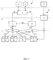
- FIG. 1 is a schematic diagram of one embodiment of a lithography system 1 with control and data interfaces according to the invention.
- the diagram shows a hierarchical arrangement with three interfaces, a cluster interface 3, cluster element interface 5, and the lithography subsystem interfaces 7.
- FIG. 1 illustrates a configuration with a lithography system cluster comprising one lithography element 10, which comprises multiple lithography subsystems 16.
- the lithography system may comprise multiple lithography elements 10, e.g. as in the FIG. 2 embodiment.
- the cluster interface 3 comprises interfaces for communication between a lithography cluster front-end 6 and one or more host systems 2, and/or between the cluster front-end 6 and one or more operator consoles 4.
- the cluster element interface 5 comprises interfaces for communication between the cluster front-end 6 and a lithography element network comprising a element control unit 12 and/or a data network hub 14.
- the element control unit 12 may be in communication with a data network hub 14 via link 106, wherein the communication is preferably uni-directional from the element control unit 12 to the data network hub 14.
- the lithography subsystem interface 7 comprises interfaces between the element control unit 12 and the lithography subsystems 16, and between the data network hub 14 and the lithography subsystems 16.
- the subsystems 16 communicate with the element control unit 12 via control network 120, and the subsystems 16 communicate with the data network hub 14 via data network 140.
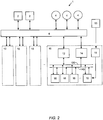
- FIG. 2 is a schematic diagram of an embodiment of a lithography system 1 in which the lithography system cluster comprises multiple lithography elements 10, each element comprising multiple lithography subsystems 16. Each element comprises a element control unit 12 and data network hub 14 communicating with the lithography subsystems 16 for the element. Each element functions as a stand-alone lithography element which is able to operate independently to expose wafers using a lithography process.
- the multiple lithography elements 10 each communicate with a single front-end 6, and the front-end 6 communicates with one or more host systems 2 and/or operator interfaces 4 which function for the entire cluster.
- FIGS. 1 and 2 are preferably designed to facilitate efficient control of a cluster of lithography elements.
- Each lithography element 10 preferably only has network interfaces, to the control network 120 and data network 140.
- An exception to this design rule is the data path 20 directly connecting the pattern streamer 19 to the subsystem(s) responsible for modulating or switching the charged particle beams.
- the pattern data is initially prepared in the pattern data processing system 18 and sent to pattern streamer 19 for data conversion and streaming to the subsystems. This design is due to the extremely high volume of pattern data transferred to the relevant subsystem(s).
- the pattern data is typically streamed to the relevant subsystems in a bit-map format, since the quantity of data is too great for local storage at the subsystem.
- the operator interfaces and interfaces to higher-level host supervisory and automation computers are made not with the individual lithography elements but at the cluster front-end 6. This enables such interfaces to be developed for the cluster without requiring knowledge of the interface protocol to the lithography elements 10 and without placing additional demands and interfering with communication across the control network 120 and data network 140.
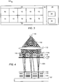
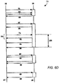
- FIG. 3 shows a simplified top view of a lithography system cluster 1.
- the cluster comprises a group of ten lithography elements 10, arranged back-to-back in two rows of five. Directly adjacent to the cluster 1, floor space is reserved as service area 23.
- Each lithography element comprises an electron-optical column contained in its own vacuum chamber, with one side of each vacuum chamber facing a substrate delivery system 22 and service area 23.
- the substrate delivery system 22 receives substrates from a substrate supply system 24 and supplies them to the lithography elements 10 for processing, and receives processed substrates from the lithography elements 10 and supplies them to the substrate supply system 24 for transfer to other systems in the fab.
- the vacuum chamber preferably encloses the charged particle source and components for generating multiple charged particle beamlets, a beam modulation system switching or modulating the beamlets, a projector system for projecting the beamlets onto a substrate to be patterned, and a moveable substrate stage.
- the vacuum chamber preferably includes a load lock system for transferring substrates into and out of the vacuum chamber from the substrate delivery system 22, and also an access door facing the service area 23 that can be opened for service access to the electron-optical column.
- Each lithography element 10 operates independently to receive and process wafers.
- Each lithography element includes its own computer processing systems for processing data and operating the components and subsystems of the lithography element.
- Each lithography subsystem 16 preferably has its own computer processor and memory system, to execute commands to direct the operations of the subsystem, collect data resulting from operation of the subsystem, and communicate with the control and data networks.
- the control element unit 12 and data network hub 14 preferably each comprise their own computer processor and memory system for performing their functions.
- the computer processor and memory systems for the control element unit 12, data network hub 14, and subsystems 16 for a lithography element 10 may be located in close proximity to the vacuum chamber for the lithography element, e.g. in a cabinet mounted above the vacuum chamber, of in a basement below the vacuum chamber, or part in each location.
- the back-to-back layout of the lithography elements of the cluster provides a system with a limited footprint, and placement of the computer processor and memory systems directly above or below the vacuum chambers also reduces the footprint.
- Floor space within a fab is valuable, and efficient use of the fab floor space is thus important.
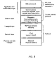
- FIG. 4 shows a simplified schematic diagram of an electron-optical column of a charged particle lithography element.
- Such lithography systems are described for example in U.S. Patent Nos. 6,897,458 ; 6,958,804 ; 7,019,908 ; 7,084,414 ; and 7,129,502 , U.S. patent publication no. 2007/0064213 , and co-pending U.S. patent application nos. 61/031,573 ; 61/031,594 ; 61/045,243 ; 61/055,839 ; 61/058,596 ; and 61/101,682 , which are all assigned to the owner of the present invention.
- the lithography element column comprises an electron source 110 producing an expanding electron beam 130, which is collimated by collimator lens system 113.
- the collimated electron beam impinges on an aperture array 114a, which blocks part of the beam to create a plurality of sub-beams 134, which pass through a condenser lens array 116 which focuses the sub-beams.
- the sub-beams impinge on a second aperture array 114b which creates a plurality of beamlets 133 from each sub-beam 134.
- the system generates a very large number of beamlets 133, preferably about 10,000 to 1,000,000 beamlets.
- a beamlet blanker array 117 comprising a plurality of blanking electrodes, deflects selected ones of the beamlets.
- the undeflected beamlets arrive at beam stop array 118 and pass through a corresponding aperture, while the deflected beamlets miss the corresponding aperture and are stopped by the beam stop array.
- the beamlet blaker array 117 and beam stop 118 operate together to switch the individual beamlets on and off.
- the undeflected beamlets pass through the beam stop array 119, and through a beam deflector array 119 which deflects the beamlets to scan the beamlets across the surface of target or substrate 121.
- the beamlets pass through projection lens arrays 120 and are projected onto substrate 121 which is positioned on a moveable stage for carrying the substrate.
- the substrate usually comprises a wafer provided with a charged-particle sensitive layer or resist layer.
- the lithography element column operates in a vacuum environment.
- a vacuum is desired to remove particles which may be ionized by the charged particle beams and become attracted to the source, may dissociate and be deposited onto the machine components, and may disperse the charged particle beams.
- a vacuum of at least 10 -6 bar is typically required.
- the charged particle lithography system is located in a vacuum chamber. All of the major elements of the lithography element are preferably housed in a common vacuum chamber, including the charged particle source, projector system for projecting the beamlets onto the substrate, and the moveable stage.
- each lithography element 10 forms an independently operating lithography element for exposing wafers.
- Each lithography element 10 comprises multiple subsystems 16 which operate to perform the functions required for the element.
- Each subsystem performs a specific function.
- Typical subsystems 16 include, for example, a wafer load subsystem (WLS), wafer positioning subsystem (WPS), an illumination optics subsystem (ILO) for generating electron beamlets, a pattern streaming subsystem (PSS) for streaming beam switching data to the lithography element, a beam switching subsystem (BSS) for switching the electron beamlets on and off, a projection optics subsystem (POS) for projecting beamlets onto the wafer, a beam measurement subsystem (BMS), a metrology subsystem (MES) etc.
- WLS wafer load subsystem
- WPS wafer positioning subsystem
- ILO illumination optics subsystem
- PSS pattern streaming subsystem
- BSS beam switching subsystem
- POS projection optics subsystem
- BMS beam measurement subsystem
- MES metrology subsystem
- Each lithography element 10 is preferably configured for receiving wafers, clamping each wafer to a chuck and preparing the clamped wafer for exposure, exposing the clamped wafer, and unclamping the exposed wafer from the chuck and presenting the exposed wafer for removal from the element.
- Each subsystem 16 may comprise one or more modules 17 which are dedicated to a particular sub-functions and are preferably designed as replaceable components.
- the modules 17 may comprise actuators 19 and sensors 21, actuators 19 which are able to perform a command and sensors 21 which are able to detect actions and results and take measurements during, before and/or after performing a command. Examples of such modules include the stage for movement of the substrate during exposure, the control computer for control of the stage, the projection lens module supplying voltages to lens arrays for projecting the beamlets onto the substrate, a vacuum pump for generating a vacuum in the vacuum chamber, etc.
- Each subsystem 16 operates independently and includes a memory for storing instructions and a computer processor for executing the instructions.
- the memory and processor may be implemented in each subsystem as a plug-in client (PIC) 15.
- PIC plug-in client
- a suitable implementation of a subsystem may include, for example, a personal computer running the Linux operating system.
- the subsystems may include a hard disk or non-volatile memory for storing their operating system so that each subsystems boots from this disk or memory.
- each subsystem may be designed with sufficient memory and processing capacity to properly perform the functions of the subsystem during its operating cycle, without needing to take into account the demands on memory and processing capacity made by the other subsystems.
- This is particularly advantageous during development and upgrade of the system, when these requirements are in flux. Disadvantages of this design are that the total required memory and processing capacity is increased, and redundancy of these components must be implemented within each subsystem. However, these disadvantages are outweighed by the simplified design leading to faster development and simpler upgrade.
- the subsystems 16 are designed to receive commands via the control network 120 and execute the commands independently from the other subsystems, reporting results for the command execution and transferring any resulting execution data upon request.
- the subsystems 16 may be designed as autonomous units, but designed to boot from a central disk or memory, for example on the data network hub. This reduces the reliability problem and cost of individual hard disks or non-volatile memory in each subsystem, and permits more easy software upgrade of a subsystem by updating the boot image for the subsystem in the central location.
- the subsystems 16 are connected via a control network to a element control unit 12, also referred to as a Support Subsystem Control or SUSC.
- the element control unit 12 comprises memory and a computer processor for controlling operation of the subsystems for the lithography element 10.
- Communication 102 between the cluster front-end 6 and SUSC 12 is designed for transfer of PPs to the SUSC 12.
- a protocol based on JavaScript Object Notation (JSON) may be used. JSON is a text-based open standard designed for human-readable data interchange, used for representing simple data structures and arrays, and is suitable for serializing and transmitting structured data over a network connection. Access to the protocol is preferably restricted to users at the cluster, and not to users outside the clean-room environment.
- the protocol preferably provides an instruction for creation of PJs, transferring the PP file and any associated parameters, to instruct the SUSC 12 to create a PJ based on the PP. Additional commands may include Abort and Cancel instructions. Communication from the SUSC 12 to the cluster front-end 6 may include acknowledgment messages, progress reporting, and error and alarm messages.
- FIG. 5 shows one embodiment of a element control unit protocol in an OSI (Open System Interconnection) layered model.
- OSI Open System Interconnection
- Communication 105 between SUSD 14 and cluster front-end 6 is designed for retrieval of PJ results, job tracing and data logging from the SUSD 14.
- a Hyper-Text Transfer Protocol (HTTP) may be used for this communication link.
- Communication 103 between the lithography subsystems 16 and SUSD 14 is designed for one-way collection of data from the subsystems 16.
- the data may be communicated using a variety of protocols, such as syslog, HDF5, UDP and others.
- High volume data may be sent using a User Datagram Protocol (UDP) to send data without the large overhead of handshaking, error checking and correction. Due to the resulting very low transmission overhead, the data can thus be regarded as being received in real-time.
- UDP User Datagram Protocol
- the hierarchical data format HDF5 may be used for transmission and storage of the high-frequency data.
- HDF5 is well suited to storing and organizing large amounts of numerical data, but is usually not used in a UDP environment.
- Other data formats such as CSV or TCP can also be used, particularly for low level (low volume) data.
- the operation of the lithography element 10 is controlled using a process program (PP) 11, which comprises a sequence of actions to be performed.
- the element control unit 12 is loaded with a PP, and schedules and executes the PP 11 as requested by a host system 2 or an operator though an operator console 4.
- the PP 11 may take the role of a recipe, e.g. as defined in the SEMI E40 standard. Although the SEMI standards specify many requirements on how to deal with recipes, the standards may be contradictory so that recipes are preferably avoided. Instead, editable and unformatted PP are used in the form of so-called Binary Large Objects (BLOBs).
- BLOBs Binary Large Objects
- the PP as the pre-planned and reusable portion of the set of instructions, settings and parameters that determines the processing environment of the wafer and that may be subject to change between runs or processing cycles.
- PPs may be designed by the lithography tool designers or generated by tooling.
- PPs may be uploaded to the lithography system by the user. PPs are used to create Process Jobs (PJs).
- a Process Job specifies the processing to be applied to a wafer or set of wafers by a lithography element 10.
- a PJ defines which PP to use when processing a specified set of wafers and may include parameters from the PP (and optionally from the user).
- a PJ is a system activity started by a user or host system.
- PPs may be used not only for controlling the processing of wafers, but also for service actions, calibration functions, lithography element testing, modifying element settings, updating and upgrading software, etc.
- no subsystem behavior occurs other than what is prescribed in a PP, with the exception of certain allowed additional categories, such as automatic initialization during power-up of a module or subsystem, periodic and unconditional behavior of a subsystem, as far as those don't influence PJ execution, and the response to an unexpected power-off, emergency or EMO activation.
- a PP is divided into steps. Most steps comprise a command and identify a subsystem which is to perform the command.
- the step may also include parameters to be used in performing the command, and parameter constraints.
- the PP may also include scheduling parameters to indicate when a step is to be performed, e.g. to be performed in parallel, in sequence, or synchronized.
- the element control unit 12 To execute a command step of the PJ, the element control unit 12 sends the command indicated in the PJ to the subsystem indicated in the relevant step of the PJ.
- the element control unit 12 monitors timing and receives the results from the subsystem. Examples of execution of specific commands are illustrated in FIGS. 6-13 and described below.
- the element control unit (SUSC) 12 converts a PP (which represents a logical plan) into a schedule of subsystem actions.
- the system may be designed so that the SUSC 12 does not have a-priori knowledge of which subsystems 16 are installed, and which subsystem commands exist and what their properties are. In this case, this information is provided to SUSC 12 at runtime by the subsystems 16 during startup.
- Each subsystem 16 may be designed to report their presence and capabilities to SUSC 12 when the subsystem is powered up and initialized.
- the subsystem establishes communication over the control network 120 and reports to SUSC 12 its identity and status, and may also report its capabilities such as which commands it is capable of performing.
- the SUSC 12 may perform a check before or during execution of a PP 11 that each subsystem required for the PP has reported its presence and a ready status, and may also check that each subsystem has reported its capability to perform the commands required for the subsystem in the PP.
- This self-reporting by the subsystems enables the lithography system to be extended or upgraded with new functionality using only localized software upgrades to the subsystems, or even with no software upgrade at all.
- a certain subsystem 16 may have its software upgraded so that it can execute a new command.
- the SUSC 12 may now be loaded with a new PP 11 which includes the new command for the upgraded subsystem.
- the upgraded subsystem 16 When the upgraded subsystem 16 is powered up it communicates with the element control unit 12, indicating its identity and status, and which commands it can execute, including the new command.
- the SUSC 12 schedules the PP to generate a PJ including the step commanding the subsystem to execute the new command.
- the SUSC 12 may perform a check that the upgraded subsystem has reported it is able to perform the new command. This upgrade thus only requires an upgrade of the relevant subsystem and of the PP, but not of SUSC 12 or any of the other subsystems 16.
- the control network 120 preferably does not use a real-time communication protocol, but nevertheless is designed to provide quasi real-time performance, providing for communication between the subsystems and SUSC 12 having high repeatability, e.g. a repeatability substantially within 1 millisecond, to provide for execution of the same job under same conditions resulting in the same timing behaviour.
- This quasi real-time performance across the control network 120 may be achieved by implementing some or all of the following measures.
- the lithography system provides a clock signal on the control network to enable synchronization of actions within the system and by the subsystems.
- the system may provide two clock signals at different frequencies to provide clocks to the subsystems for different timing accuracies, e.g. one clock signal accurate in milliseconds and one in nanoseconds.
- the pattern streaming subsystem for streaming beam switching data and the beam switching subsystem for switching the electron beamlets on and off need to exchange data at very high frequency to enable high frequency switching of the beamlets, and the beam measurement subsystem is required to send beam position measurements at very high frequency.
- Other functions that need a high precision clock include the substrate positioning system and projection optics system. These subsystems are fed by and capable of receiving nanosecond clock pulses provided by a sync clock subsystem.
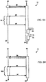
- FIGS. 6A to 6H show message sequences 30, 40, 50, 70, 80, 90, 100 supported by a protocol.
- the sequence diagrams 30, 40, 50, 70, 80, 90, 100 are annotated with required response times for the average case and for time-outs that SUSC 12 will use before closing a connection.
- the described timings are in principle round trip times involving a SUSC 12, a SUSD 14 and a subsystem 16.
- the SUSC 12 protocol communicates messages over a TCP connection.
- SUSC 12 acts as the TCP server, and the PICs 15 in the subsystems 16 act as TCP clients.
- the PICs make a connection to SUSC 12 on a specific port, and the SUSC 12 has an IP address in the control network 120. If connecting fails PIC retries until it succeeds.
- FIG. 6A shows a connect sequence 30 where a element control unit (SUSC) 12 and a PIC in a subsystem 16 connect to each other. Vertical time lines 27, 29 are shown from SUSC 12 and subsystem 16 to indicate timing of messages.
- the connect sequence begins with a standard 3-way handshake of the TCP protocol or TCP connection 33 to set up the connection at the operating system level.
- the subsystem 16 sends a connect message 35 to SUSC 12.
- SUSC 12 sends a connect reply 37 within a time period 31, preferably 0.5 seconds.
- the connect reply 37 may contain location specific information, e.g. the time zone where the machine in located. This may be used to set the time zone 39 of SUSC 12.
- the subsystem 16 may do further internal subsystem initialization 41 afterwards.
- a connection is kept open indefinitely, i.e. until one of the sides shuts down and the connection is closed. This closing occurs either by an explicit socket close by the application or automatically by the operating system as part of its shutdown sequence.
- a PIC 15 detects the closing of its connection it attempts to reconnect, and if reconnecting fails it may retry until it succeeds.
- SUSC 12 detects the closing of a connection it may discard all information of the associated PIC (such as registered commands or planned future commands) and consider the PIC 15 and associated subsystem 16 absent until it reconnects.
- SUSC 12 may consider the previous connection closed. This scenario could happen when the PIC 15 was powered off suddenly without its kernel being given an opportunity to close TCP connections and the SUSC 12 hasn't attempted communication with this PIC yet.
- FIG. 6B shows a reconnect sequence 40 which is started when a subsystem 16 has already been initialized, but has lost its connection to SUSC 12. It is the responsibility of the subsystem 16 to reconnect to SUSC 12. A repeat will be done by the subsystem 16 sending a connect message 35 to SUSC 12, and upon receiving the connect message 35, SUSC 12 sends a connect reply 37 message back to the subsystem 16. Here, also, within a time period 31, preferably 0.5 seconds. The reconnect sequence 40 will be repeated until the subsystem 16 is connected to SUSC 12.
- FIG. 6C shows an execute command sequence 50 which starts optionally with the transfer of input arguments with a 'set' command 51 to subsystem 16 by SUSC 12.
- the set command 51 is followed by N times an amount of data 52 sent to subsystem 16.
- subsystem 16 acknowledges the received command 51 and data 52 by sending a set reply 53 (setReply) back to SUSC 12.
- Any reply sent from the subsystem 16 to SUSC 12 has a reply time period 55, which comprises preferably less than an average of 0.5 milliseconds.
- the set reply 53 must be sent within a time-out limit 54, which comprises preferably 30.0 seconds plus minus 1.0 seconds. If a reply is not received, SUSC 12 will consider subsystem 16 to be either not connected or defective.
- subsystem 16 After SUSC 12 sends an execute command 57, subsystem 16 acknowledges preferably within the reply time period 55 with an executeStarted reply 58. After subsystem 16 has finished execution, it sends an executeDone 59 to SUSC 12. The output arguments (if any) are retrieved with the 'get' command 60 sent by SUSC 12. Subsystem 16 acknowledges with a getReply 61 and thereafter sends an N amount of data 62 or output arguments.
- Input and output arguments that are no longer needed for future execute commands 57 are removed from subsystem 16 using the delete command 63.
- the subsystem 16 will preferably reply within the reply time period 55 with a deleteReply 64. In one version of the protocol inputs and outputs are not carried over from one interface command to the other.
- the subsystem 16 can safely assume no more inputs will be sent than needed for the next command, and it can safely assume that all inputs and outputs will be deleted before inputs of the next commands are sent.
- FIG. 6D shows an abort sequence 70 which illustrates the order of events in the case of an aborted execute command 71.
- the abort sequence 70 is globally the same as a normal execute sequence 50 with the following differences.
- SUSC 12 sends an abort request 71 in the period between receiving the executeStarted 58 and executeDone 59 messages.
- the subsystem 16 in turn sends an abortReply 72.
- Sending an abortReply 72 to SUSC 12, as a response to the abort request 71, must be done within a time period abortReply 74, which comprises of 90.0 seconds plus or minus 1.0 second, where the 90 seconds comprise 60 seconds for the maximum polling interval plus an additional 30 seconds.
- the command runs to completion or breaks off before the command is finished. If the command was not finished, an exception 91 may be logged. Also, not all output arguments may be available and empty ones (0 byte) may be substituted by the subsystem 16. The SUSC 12 will try to retrieve them all. It is possible that the abort message 71 from SUSC 12 and the executeDone 59 from the subsystem 16 cross each other. In that case the sequence 80 shown in FIG. 6E is applicable.
- FIG. 6E shows an abort sequence with a race condition 80.
- a race condition 81 is a condition which occurs when two or more messages cross each other.
- the abort message 71 crosses with the executeDone message 59.
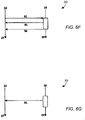
- FIG. 6F, 6G , and 6H show three cases for an exception sequence 90.
- Exception messages are sent to SUSC 12 by a subsystem 16 when an exception 90 occurs in the form of, for example, an error or an alarm.
- An error is used to communicate to the user 4 that the lithographic element is not behaving as expected.
- An alarm is a condition that must be acknowledged by the user 4.
- Exceptions 91 that occur within the context of executing an interface command may be tagged with context information. For exceptions 91 that occur outside the context of such command (spontaneous exceptions 90) these context fields may be left empty or the most appropriate context of an already completed command that is related to the failure may be supplied.
- Exceptions 91 are intended to notify the operator 4 of error situations, to guide the operator 4 through a recovery procedure and to communicate the essence of a problem in a concise manner, for example by telephone or trouble ticket title. Exceptions 91 should therefore not be considered as a debugging information channel for module designers. Alternatively, PJ outputs in human readable data formats may be used for information that could be monitored or investigated offline.
- Exception messages 91 do not terminate protocol sequences and are no reason to stop handling future commands. For example, after a interface command fails and an exception 91 is logged by a data network hub 14, executeDone 59 may still be sent and outputs made available to 'get'. The subsystem 16 should also be ready to accept new interface commands to recover from the situation.
- An exception 91 is allowed to be inserted at any time in the protocol, except within the getReply 61 sequence. If any exceptions 91 can be generated by a parallel thread the PIC 16 designer could consider to allocate a dedicated PIC 16 connection for logging such exceptions 91 and not for any commands. That avoids this interference in a straightforward manner.
- FIG. 6F shows an exception 91 generated by the subsystem 16 during a generic or any protocol command 92 sent from SUSC 12.
- the subsystem 16 also sends an any protocol command reply 93 to SUSC 12.
- FIG. 6G shows a spontaneous exception 91
- FIG 6H shows an exception 91 sent from the subsystem 16 to SUSC 12 during an execute command 57.
- any protocol command 92 an exception 91 can be raised.
- the command is terminated normally with the associated reply message.
- the get 60 and delete 63 commands are executed as though no exception 91 has occurred. However, it is possible that due to the occurrence of the exception 91 some output arguments may be empty (0 bytes).
- the subsystems 16 are connected via data network 140 to data network hub 14. Data collection, storage and management is performed via the data network 140.
- the control network 120 forms a control network path between the element control unit 12 and the lithography subsystems 16, and the data network 140 forms a data network path between the data network hub 14 and the lithography subsystems 16.
- the control network 120 and data network 140 are physically separate networks, Each network has its own separate physical media, including wiring, network components such as switches, and network connections to the subsystems 16. Thus the control network path and the data network path comprise physically separate media and form separate and independent communication paths.
- Each lithography subsystem 16 has a connection to the control network 140 adapted to receive and transmit control information from and to the element control unit 12 via the control network.
- Each lithography subsystem 16 has a separate connection to the data network 140, adapted to transmit data information to the data network hub 14 via the data network.
- the data network 140 is designed with a bandwidth much greater than the transmission rates used by the subsystems 16.
- the data network 140 may have a bandwidth of 1 Gbit/s and the subsystems designed to transmit at 100 Mbit/s.
- a data exchange cap is set at 140 Mbit between the subsystems 16 and the data network 140, whereas a cap of 1 Gbit is set on a data exchange between the data network 140 and SUSD 14.
- a network switch is included in the data network 140 to merge traffic, to prevent (data) package collision.
- the data network hub 14 is adapted to continuously log data received from the subsystems 16. This data may include measurement data taken by the subsystems during a execution of a PJ, settings of the subsystems, and data for debugging and fault tracing.
- the data network hub 14 preferably is always logging all data, including low-level tracing data, so there is no need to turn on data logging. This continual data logging speeds up problem diagnosis, reducing the need to rerun and reproduce an error or problem.
- the element control unit 12 is connected to the data network hub 14 to send information relating to the progress of PJs executing in the element control unit 12 for logging by the data network hub 14.
- the data network hub 14 continuously logs the data received from the element control unit 12.
- Data network hub 14 includes very large data storage capacity, sufficient for storage of very large quantities of low level data from all subsystems 16 over a long operating time period, e.g. in the order of months or years.
- the data stored by data network hub 14 is organized and tagged, preferably with a time stamp and PJ identifier.
- the stored data can be retrieved from the data network hub 14 and analyzed and filtered, preferably off-line.
- Separation of data collection via the data network 140 from control communications via the control network 120 enables high frequency collection of high volume data across the data network without compromising communications across the control network.
- the control network is enabled to operate in quasi real-time by controlling congestion on the control network 120, and avoiding the high volume traffic present on the data network 140.
- Separation of data management and storage functions in the data network hub 14 and PJ execution in the element control unit 12 enables processing of high volumes of data by the data network hub 14 without compromising the processing of PJs by the element control unit 12.
- the separation of control and data collection and management enables a simpler design without needing to account for interaction between the two systems.
Landscapes
- Engineering & Computer Science (AREA)
- Physics & Mathematics (AREA)
- General Physics & Mathematics (AREA)
- Chemical & Material Sciences (AREA)
- Nanotechnology (AREA)
- Theoretical Computer Science (AREA)
- Crystallography & Structural Chemistry (AREA)
- Software Systems (AREA)
- Computer Networks & Wireless Communication (AREA)
- Public Health (AREA)
- Manufacturing & Machinery (AREA)
- Analytical Chemistry (AREA)
- Health & Medical Sciences (AREA)
- Environmental & Geological Engineering (AREA)
- Epidemiology (AREA)
- General Engineering & Computer Science (AREA)
- Mathematical Physics (AREA)
- Condensed Matter Physics & Semiconductors (AREA)
- Quality & Reliability (AREA)
- Automation & Control Theory (AREA)
- Exposure And Positioning Against Photoresist Photosensitive Materials (AREA)
- Exposure Of Semiconductors, Excluding Electron Or Ion Beam Exposure (AREA)
- Electron Beam Exposure (AREA)
- General Factory Administration (AREA)
- Container, Conveyance, Adherence, Positioning, Of Wafer (AREA)
Applications Claiming Priority (3)
| Application Number | Priority Date | Filing Date | Title |
|---|---|---|---|
| US201161478117P | 2011-04-22 | 2011-04-22 | |
| US201161533673P | 2011-09-12 | 2011-09-12 | |
| PCT/EP2012/057366 WO2012143548A2 (en) | 2011-04-22 | 2012-04-23 | Network architecture and protocol for cluster of lithography machines |
Publications (2)
| Publication Number | Publication Date |
|---|---|
| EP2699966A2 EP2699966A2 (en) | 2014-02-26 |
| EP2699966B1 true EP2699966B1 (en) | 2021-04-07 |
Family
ID=45998374
Family Applications (2)
| Application Number | Title | Priority Date | Filing Date |
|---|---|---|---|
| EP12719948.7A Active EP2700081B1 (en) | 2011-04-22 | 2012-04-23 | Network architecture for lithography machine cluster |
| EP12716017.4A Active EP2699966B1 (en) | 2011-04-22 | 2012-04-23 | Network architecture and protocol for cluster of lithography machines |
Family Applications Before (1)
| Application Number | Title | Priority Date | Filing Date |
|---|---|---|---|
| EP12719948.7A Active EP2700081B1 (en) | 2011-04-22 | 2012-04-23 | Network architecture for lithography machine cluster |
Country Status (8)
| Country | Link |
|---|---|
| US (3) | US9086912B2 (zh) |
| EP (2) | EP2700081B1 (zh) |
| JP (3) | JP6042410B2 (zh) |
| KR (2) | KR102072200B1 (zh) |
| CN (2) | CN105974743B (zh) |
| RU (1) | RU2573398C2 (zh) |
| TW (2) | TWI526789B (zh) |
| WO (2) | WO2012143555A2 (zh) |
Families Citing this family (16)
| Publication number | Priority date | Publication date | Assignee | Title |
|---|---|---|---|---|
| WO2012080278A1 (en) * | 2010-12-14 | 2012-06-21 | Mapper Lithography Ip B.V. | Lithography system and method of processing substrates in such a lithography system |
| US8893059B2 (en) | 2012-02-06 | 2014-11-18 | Kla-Tencor Corporation | Pattern data system for high-performance maskless electron beam lithography |
| JP2014204012A (ja) * | 2013-04-05 | 2014-10-27 | キヤノン株式会社 | 描画装置、及び物品の製造方法 |
| CN103389625A (zh) * | 2013-07-11 | 2013-11-13 | 浙江大学 | 一种应用于浸没式光刻机中浸液液体传送系统的通讯方法 |
| JP6312379B2 (ja) * | 2013-07-19 | 2018-04-18 | キヤノン株式会社 | リソグラフィ装置、リソグラフィ方法、リソグラフィシステム、プログラム、物品の製造方法 |
| JP2015204401A (ja) * | 2014-04-15 | 2015-11-16 | キヤノン株式会社 | リソグラフィ装置、および物品の製造方法 |
| US9927725B2 (en) | 2015-02-16 | 2018-03-27 | Canon Kabushiki Kaisha | Lithography apparatus, lithography method, program, lithography system, and article manufacturing method |
| JP6198805B2 (ja) * | 2015-02-16 | 2017-09-20 | キヤノン株式会社 | リソグラフィ装置、リソグラフィ方法、プログラム、リソグラフィシステムおよび物品製造方法 |
| US10527950B2 (en) * | 2016-07-19 | 2020-01-07 | Asml Netherlands B.V. | Apparatus for direct write maskless lithography |
| NL2019502B1 (en) * | 2016-09-08 | 2018-08-31 | Mapper Lithography Ip Bv | Method and system for fabricating unique chips using a charged particle multi-beamlet lithography system |
| US10522472B2 (en) | 2016-09-08 | 2019-12-31 | Asml Netherlands B.V. | Secure chips with serial numbers |
| US20180068047A1 (en) | 2016-09-08 | 2018-03-08 | Mapper Lithography Ip B.V. | Method and system for fabricating unique chips using a charged particle multi-beamlet lithography system |
| US10418324B2 (en) | 2016-10-27 | 2019-09-17 | Asml Netherlands B.V. | Fabricating unique chips using a charged particle multi-beamlet lithography system |
| CN106647181B (zh) * | 2016-12-19 | 2018-03-09 | 电子科技大学 | 一种用于dmd无掩膜光刻机的高速图像曝光方法 |
| EP3514640B1 (de) | 2018-01-18 | 2023-05-17 | Gebr. Saacke GmbH & Co.KG | Vorrichtung und verfahren zur bereitstellung von maschinendaten |
| CN115297183B (zh) * | 2022-07-29 | 2023-11-03 | 天翼云科技有限公司 | 一种数据处理方法、装置、电子设备和存储介质 |
Family Cites Families (64)
| Publication number | Priority date | Publication date | Assignee | Title |
|---|---|---|---|---|
| US3157308A (en) | 1961-09-05 | 1964-11-17 | Clark Mfg Co J L | Canister type container and method of making the same |
| US3159408A (en) | 1961-10-05 | 1964-12-01 | Grace W R & Co | Chuck |
| US4524308A (en) | 1984-06-01 | 1985-06-18 | Sony Corporation | Circuits for accomplishing electron beam convergence in color cathode ray tubes |
| JP3336436B2 (ja) | 1991-04-02 | 2002-10-21 | 株式会社ニコン | リソグラフィシステム、情報収集装置、露光装置、及び半導体デバイス製造方法 |
| WO1994025880A1 (en) | 1993-04-30 | 1994-11-10 | Board Of Regents, The University Of Texas System | Megavoltage scanning imager and method for its use |
| TW276353B (zh) | 1993-07-15 | 1996-05-21 | Hitachi Seisakusyo Kk | |
| EP0766405A1 (en) | 1995-09-29 | 1997-04-02 | STMicroelectronics S.r.l. | Successive approximation register without redundancy |
| US5778386A (en) | 1996-05-28 | 1998-07-07 | Taiwan Semiconductor Manufacturing Company Ltd. | Global view storage management system for semiconductor manufacturing plants |
| JP3087696B2 (ja) * | 1997-07-25 | 2000-09-11 | 日本電気株式会社 | 分散メモリ型マルチプロセッサ・システム制御方法およびコンピュータ読み取り可能な記録媒体 |
| KR19990062942A (ko) * | 1997-12-10 | 1999-07-26 | 히로시 오우라 | 전하 입자 빔 노출 장치 |
| US6011952A (en) * | 1998-01-20 | 2000-01-04 | Viasat, Inc. | Self-interference cancellation for relayed communication networks |
| US6610150B1 (en) * | 1999-04-02 | 2003-08-26 | Asml Us, Inc. | Semiconductor wafer processing system with vertically-stacked process chambers and single-axis dual-wafer transfer system |
| RU2258253C2 (ru) * | 2000-02-16 | 2005-08-10 | Саймер, Инк. | Система контроля технологического процесса для лазеров, используемых в литографии |
| US6714830B2 (en) * | 2000-02-28 | 2004-03-30 | Canon Kabushiki Kaisha | Push-type scheduling for semiconductor fabrication |
| WO2001084382A1 (en) | 2000-05-04 | 2001-11-08 | Kla-Tencor, Inc. | Methods and systems for lithography process control |
| US7149792B1 (en) * | 2000-11-20 | 2006-12-12 | Axeda Corporation | Device registration mechanism |
| JP2002252161A (ja) | 2001-02-23 | 2002-09-06 | Hitachi Ltd | 半導体製造システム |
| JP4713773B2 (ja) * | 2001-07-09 | 2011-06-29 | 株式会社アドバンテスト | 電子ビーム露光装置及び電子ビーム露光方法 |
| US7280883B2 (en) * | 2001-09-06 | 2007-10-09 | Dainippon Screen Mfg. Co., Ltd. | Substrate processing system managing apparatus information of substrate processing apparatus |
| JP2003288496A (ja) | 2002-03-27 | 2003-10-10 | Toshiba Corp | 描画支援システム、描画支援方法、マスク製造支援システム、及びマスク製造支援方法 |
| JP4078150B2 (ja) | 2002-08-22 | 2008-04-23 | 株式会社日立ハイテクノロジーズ | 半導体製造装置 |
| KR100523839B1 (ko) * | 2002-10-07 | 2005-10-27 | 한국전자통신연구원 | 건식 리소그라피 방법 및 이를 이용한 게이트 패턴 형성방법 |
| EP2302459A3 (en) | 2002-10-25 | 2011-04-06 | Mapper Lithography Ip B.V. | Lithography system |
| JP5053514B2 (ja) | 2002-10-30 | 2012-10-17 | マッパー・リソグラフィー・アイピー・ビー.ブイ. | 電子ビーム露光システム |
| WO2004081910A2 (en) | 2003-03-10 | 2004-09-23 | Mapper Lithography Ip B.V. | Apparatus for generating a plurality of beamlets |
| CN100543920C (zh) | 2003-05-28 | 2009-09-23 | 迈普尔平版印刷Ip有限公司 | 带电粒子小射束曝光系统 |
| EP1660945B1 (en) | 2003-07-30 | 2007-12-19 | Mapper Lithography Ip B.V. | Modulator circuitry |
| US7094613B2 (en) * | 2003-10-21 | 2006-08-22 | Applied Materials, Inc. | Method for controlling accuracy and repeatability of an etch process |
| JP2005174959A (ja) * | 2003-12-05 | 2005-06-30 | Nikon Corp | リソグラフィシステム、プログラム及び情報記録媒体、支援装置、並びに露光方法 |
| US7728880B2 (en) * | 2004-06-25 | 2010-06-01 | Qualcomm Incorporated | Automatic white balance method and apparatus |
| JP2006113705A (ja) * | 2004-10-13 | 2006-04-27 | Nikon Corp | 情報処理システム及びプログラム |
| DE102004055149B4 (de) * | 2004-11-16 | 2007-07-19 | Leica Microsystems Lithography Gmbh | Vorrichtung und Verfahren zum Abbilden eines Mehrfach-Partikelstrahls auf ein Substrat |
| CN100361113C (zh) * | 2005-02-05 | 2008-01-09 | 上海微电子装备有限公司 | 步进扫描投影光刻机的高速同步广播总线系统 |
| JP2006338232A (ja) * | 2005-06-01 | 2006-12-14 | Murata Mach Ltd | 通信システム |
| US20070010905A1 (en) | 2005-07-07 | 2007-01-11 | Taiwan Semiconductor Manufacturing Co., Ltd. | Systems and methods for monitoring processing tool |
| US7709815B2 (en) | 2005-09-16 | 2010-05-04 | Mapper Lithography Ip B.V. | Lithography system and projection method |
| US8055727B2 (en) * | 2005-09-22 | 2011-11-08 | Fisher-Rosemount Systems, Inc. | Use of a really simple syndication communication format in a process control system |
| JP5061904B2 (ja) * | 2005-10-28 | 2012-10-31 | 株式会社ニコン | デバイス製造処理装置間の接続装置及び接続方法、プログラム、デバイス製造処理システム、露光装置及び露光方法、並びに測定検査装置及び測定検査方法 |
| US8090875B2 (en) | 2005-10-28 | 2012-01-03 | Nikon Corporation | Device and method for connecting device manufacturing processing apparatuses, program, device manufacturing processing system, exposure apparatus and method, and measurement and inspection apparatus and method |
| US7652749B2 (en) | 2006-02-14 | 2010-01-26 | Asml Netherlands B.V. | Software upgrades in a lithographic apparatus |
| TW200745771A (en) * | 2006-02-17 | 2007-12-16 | Nikon Corp | Adjustment method, substrate processing method, substrate processing apparatus, exposure apparatus, inspection apparatus, measurement and/or inspection system, processing apparatus, computer system, program and information recording medium |
| US8134681B2 (en) * | 2006-02-17 | 2012-03-13 | Nikon Corporation | Adjustment method, substrate processing method, substrate processing apparatus, exposure apparatus, inspection apparatus, measurement and/or inspection system, processing apparatus, computer system, program and information recording medium |
| JP4682107B2 (ja) * | 2006-08-28 | 2011-05-11 | 株式会社リコー | 画像形成装置、情報処理方法及び情報処理プログラム |
| US7801635B2 (en) * | 2007-01-30 | 2010-09-21 | Tokyo Electron Limited | Real-time parameter tuning for etch processes |
| US8636458B2 (en) | 2007-06-06 | 2014-01-28 | Asml Netherlands B.V. | Integrated post-exposure bake track |
| JP4992750B2 (ja) * | 2008-02-14 | 2012-08-08 | 日本電気株式会社 | 中継装置 |
| WO2009106397A1 (en) | 2008-02-26 | 2009-09-03 | Mapper Lithography Ip B.V. | Projection lens arrangement |
| US8445869B2 (en) | 2008-04-15 | 2013-05-21 | Mapper Lithography Ip B.V. | Projection lens arrangement |
| JP5619629B2 (ja) | 2008-02-26 | 2014-11-05 | マッパー・リソグラフィー・アイピー・ビー.ブイ. | 投影レンズ構成体 |
| US8258484B2 (en) | 2008-04-15 | 2012-09-04 | Mapper Lithography Ip B.V. | Beamlet blanker arrangement |
| JP5587299B2 (ja) | 2008-05-23 | 2014-09-10 | マッパー・リソグラフィー・アイピー・ビー.ブイ. | 結像システム |
| WO2009147202A1 (en) | 2008-06-04 | 2009-12-10 | Mapper Lithography Ip B.V. | Writing strategy |
| JP2010067759A (ja) * | 2008-09-10 | 2010-03-25 | Canon Inc | 露光装置 |
| JP5420670B2 (ja) | 2008-10-01 | 2014-02-19 | マッパー・リソグラフィー・アイピー・ビー.ブイ. | 静電レンズ構造体 |
| JP2010093125A (ja) * | 2008-10-09 | 2010-04-22 | Toray Eng Co Ltd | 基板処理システムおよび基板処理方法 |
| KR20110084318A (ko) * | 2008-12-15 | 2011-07-21 | 도쿄엘렉트론가부시키가이샤 | 기판 처리 시스템, 기판 처리 방법 및 프로그램을 기억한 기억 매체 |
| WO2010076863A1 (ja) * | 2008-12-29 | 2010-07-08 | キヤノンアネルバ株式会社 | 基板処理システム及び基板処理装置 |
| NL2004392A (en) * | 2009-04-15 | 2010-10-18 | Asml Netherlands Bv | Lithographic apparatus, control system, multi-core processor, and a method to start tasks on a multi-core processor. |
| EP2433295A2 (en) | 2009-05-20 | 2012-03-28 | Mapper Lithography IP B.V. | Dual pass scanning |
| CN102460633B (zh) * | 2009-05-20 | 2014-12-17 | 迈普尔平版印刷Ip有限公司 | 用于光刻系统的图案数据转换器 |
| JP2011054679A (ja) * | 2009-08-31 | 2011-03-17 | Hitachi Kokusai Electric Inc | 基板処理装置 |
| JP5392190B2 (ja) | 2010-06-01 | 2014-01-22 | 東京エレクトロン株式会社 | 基板処理システム及び基板処理方法 |
| US8822106B2 (en) * | 2012-04-13 | 2014-09-02 | Taiwan Semiconductor Manufacturing Company, Ltd. | Grid refinement method |
| US10168208B2 (en) | 2015-04-03 | 2019-01-01 | Hitachi High-Technologies Corporation | Light amount detection device, immune analyzing apparatus and charged particle beam apparatus that each use the light amount detection device |
-
2012
- 2012-04-23 TW TW101114467A patent/TWI526789B/zh active
- 2012-04-23 KR KR1020177029925A patent/KR102072200B1/ko active IP Right Grant
- 2012-04-23 WO PCT/EP2012/057385 patent/WO2012143555A2/en unknown
- 2012-04-23 RU RU2013151876/07A patent/RU2573398C2/ru active
- 2012-04-23 WO PCT/EP2012/057366 patent/WO2012143548A2/en active Search and Examination
- 2012-04-23 JP JP2014505667A patent/JP6042410B2/ja active Active
- 2012-04-23 KR KR1020137030924A patent/KR101791252B1/ko active IP Right Grant
- 2012-04-23 CN CN201610308354.1A patent/CN105974743B/zh active Active
- 2012-04-23 US US13/452,990 patent/US9086912B2/en active Active
- 2012-04-23 TW TW101114468A patent/TWI576670B/zh active
- 2012-04-23 EP EP12719948.7A patent/EP2700081B1/en active Active
- 2012-04-23 EP EP12716017.4A patent/EP2699966B1/en active Active
- 2012-04-23 CN CN201280030773.3A patent/CN103649836B/zh active Active
- 2012-04-23 US US13/453,008 patent/US9244726B2/en active Active
- 2012-04-23 JP JP2014505664A patent/JP5951753B2/ja active Active
-
2015
- 2015-06-15 US US14/738,962 patent/US9507629B2/en active Active
-
2016
- 2016-05-23 JP JP2016102480A patent/JP6550623B2/ja active Active
Non-Patent Citations (1)
| Title |
|---|
| None * |
Also Published As
Similar Documents
| Publication | Publication Date | Title |
|---|---|---|
| US9507629B2 (en) | Network architecture and protocol for cluster of lithography machines | |
| Choi et al. | Fboss: building switch software at scale | |
| US6480854B1 (en) | Method and apparatus for increasing database availability | |
| CN1529835A (zh) | 使用基线控制脚本控制工具的方法和装置 | |
| JP2005520324A (ja) | 障害検出データを仲介するためのシステム | |
| US7684654B2 (en) | System and method for fault detection and recovery in a medical imaging system | |
| US6754302B2 (en) | X-ray exposure apparatus | |
| US8516145B2 (en) | Information processing method and information processing apparatus for transmitting data generated by device manufacturing apparatus | |
| US20210019186A1 (en) | Information processing system, information processing apparatus, and method of controlling an information processing system | |
| JP7336207B2 (ja) | 基板処理システム、基板処理システムの制御方法、プログラム、および物品製造方法 | |
| CN110544651B (zh) | 基板处理系统、其控制方法、存储介质和物品的制造方法 | |
| JPH11232143A (ja) | マルチスレッドの監視方法 |
Legal Events
| Date | Code | Title | Description |
|---|---|---|---|
| PUAI | Public reference made under article 153(3) epc to a published international application that has entered the european phase |
Free format text: ORIGINAL CODE: 0009012 |
|
| 17P | Request for examination filed |
Effective date: 20131122 |
|
| AK | Designated contracting states |
Kind code of ref document: A2 Designated state(s): AL AT BE BG CH CY CZ DE DK EE ES FI FR GB GR HR HU IE IS IT LI LT LU LV MC MK MT NL NO PL PT RO RS SE SI SK SM TR |
|
| DAX | Request for extension of the european patent (deleted) | ||
| 17Q | First examination report despatched |
Effective date: 20151223 |
|
| 17Q | First examination report despatched |
Effective date: 20160303 |
|
| 19U | Interruption of proceedings before grant |
Effective date: 20190103 |
|
| 19W | Proceedings resumed before grant after interruption of proceedings |
Effective date: 20190801 |
|
| RAP1 | Party data changed (applicant data changed or rights of an application transferred) |
Owner name: ASML NETHERLANDS B.V. |
|
| GRAP | Despatch of communication of intention to grant a patent |
Free format text: ORIGINAL CODE: EPIDOSNIGR1 |
|
| STAA | Information on the status of an ep patent application or granted ep patent |
Free format text: STATUS: GRANT OF PATENT IS INTENDED |
|
| INTG | Intention to grant announced |
Effective date: 20201222 |
|
| GRAS | Grant fee paid |
Free format text: ORIGINAL CODE: EPIDOSNIGR3 |
|
| GRAA | (expected) grant |
Free format text: ORIGINAL CODE: 0009210 |
|
| STAA | Information on the status of an ep patent application or granted ep patent |
Free format text: STATUS: THE PATENT HAS BEEN GRANTED |
|
| AK | Designated contracting states |
Kind code of ref document: B1 Designated state(s): AL AT BE BG CH CY CZ DE DK EE ES FI FR GB GR HR HU IE IS IT LI LT LU LV MC MK MT NL NO PL PT RO RS SE SI SK SM TR |
|
| REG | Reference to a national code |
Ref country code: GB Ref legal event code: FG4D |
|
| REG | Reference to a national code |
Ref country code: AT Ref legal event code: REF Ref document number: 1380473 Country of ref document: AT Kind code of ref document: T Effective date: 20210415 Ref country code: CH Ref legal event code: EP |
|
| REG | Reference to a national code |
Ref country code: DE Ref legal event code: R096 Ref document number: 602012075100 Country of ref document: DE |
|
| REG | Reference to a national code |
Ref country code: IE Ref legal event code: FG4D |
|
| REG | Reference to a national code |
Ref country code: LT Ref legal event code: MG9D |
|
| REG | Reference to a national code |
Ref country code: NL Ref legal event code: MP Effective date: 20210407 Ref country code: AT Ref legal event code: MK05 Ref document number: 1380473 Country of ref document: AT Kind code of ref document: T Effective date: 20210407 |
|
| PG25 | Lapsed in a contracting state [announced via postgrant information from national office to epo] |
Ref country code: NL Free format text: LAPSE BECAUSE OF FAILURE TO SUBMIT A TRANSLATION OF THE DESCRIPTION OR TO PAY THE FEE WITHIN THE PRESCRIBED TIME-LIMIT Effective date: 20210407 Ref country code: LT Free format text: LAPSE BECAUSE OF FAILURE TO SUBMIT A TRANSLATION OF THE DESCRIPTION OR TO PAY THE FEE WITHIN THE PRESCRIBED TIME-LIMIT Effective date: 20210407 Ref country code: FI Free format text: LAPSE BECAUSE OF FAILURE TO SUBMIT A TRANSLATION OF THE DESCRIPTION OR TO PAY THE FEE WITHIN THE PRESCRIBED TIME-LIMIT Effective date: 20210407 Ref country code: AT Free format text: LAPSE BECAUSE OF FAILURE TO SUBMIT A TRANSLATION OF THE DESCRIPTION OR TO PAY THE FEE WITHIN THE PRESCRIBED TIME-LIMIT Effective date: 20210407 Ref country code: BG Free format text: LAPSE BECAUSE OF FAILURE TO SUBMIT A TRANSLATION OF THE DESCRIPTION OR TO PAY THE FEE WITHIN THE PRESCRIBED TIME-LIMIT Effective date: 20210707 Ref country code: HR Free format text: LAPSE BECAUSE OF FAILURE TO SUBMIT A TRANSLATION OF THE DESCRIPTION OR TO PAY THE FEE WITHIN THE PRESCRIBED TIME-LIMIT Effective date: 20210407 |
|
| PG25 | Lapsed in a contracting state [announced via postgrant information from national office to epo] |
Ref country code: SE Free format text: LAPSE BECAUSE OF FAILURE TO SUBMIT A TRANSLATION OF THE DESCRIPTION OR TO PAY THE FEE WITHIN THE PRESCRIBED TIME-LIMIT Effective date: 20210407 Ref country code: RS Free format text: LAPSE BECAUSE OF FAILURE TO SUBMIT A TRANSLATION OF THE DESCRIPTION OR TO PAY THE FEE WITHIN THE PRESCRIBED TIME-LIMIT Effective date: 20210407 Ref country code: GR Free format text: LAPSE BECAUSE OF FAILURE TO SUBMIT A TRANSLATION OF THE DESCRIPTION OR TO PAY THE FEE WITHIN THE PRESCRIBED TIME-LIMIT Effective date: 20210708 Ref country code: IS Free format text: LAPSE BECAUSE OF FAILURE TO SUBMIT A TRANSLATION OF THE DESCRIPTION OR TO PAY THE FEE WITHIN THE PRESCRIBED TIME-LIMIT Effective date: 20210807 Ref country code: LV Free format text: LAPSE BECAUSE OF FAILURE TO SUBMIT A TRANSLATION OF THE DESCRIPTION OR TO PAY THE FEE WITHIN THE PRESCRIBED TIME-LIMIT Effective date: 20210407 Ref country code: PT Free format text: LAPSE BECAUSE OF FAILURE TO SUBMIT A TRANSLATION OF THE DESCRIPTION OR TO PAY THE FEE WITHIN THE PRESCRIBED TIME-LIMIT Effective date: 20210809 Ref country code: PL Free format text: LAPSE BECAUSE OF FAILURE TO SUBMIT A TRANSLATION OF THE DESCRIPTION OR TO PAY THE FEE WITHIN THE PRESCRIBED TIME-LIMIT Effective date: 20210407 Ref country code: NO Free format text: LAPSE BECAUSE OF FAILURE TO SUBMIT A TRANSLATION OF THE DESCRIPTION OR TO PAY THE FEE WITHIN THE PRESCRIBED TIME-LIMIT Effective date: 20210707 Ref country code: ES Free format text: LAPSE BECAUSE OF FAILURE TO SUBMIT A TRANSLATION OF THE DESCRIPTION OR TO PAY THE FEE WITHIN THE PRESCRIBED TIME-LIMIT Effective date: 20210407 |
|
| PG25 | Lapsed in a contracting state [announced via postgrant information from national office to epo] |
Ref country code: LU Free format text: LAPSE BECAUSE OF NON-PAYMENT OF DUE FEES Effective date: 20210423 |
|
| REG | Reference to a national code |
Ref country code: DE Ref legal event code: R097 Ref document number: 602012075100 Country of ref document: DE |
|
| REG | Reference to a national code |
Ref country code: BE Ref legal event code: MM Effective date: 20210430 |
|
| PG25 | Lapsed in a contracting state [announced via postgrant information from national office to epo] |
Ref country code: EE Free format text: LAPSE BECAUSE OF FAILURE TO SUBMIT A TRANSLATION OF THE DESCRIPTION OR TO PAY THE FEE WITHIN THE PRESCRIBED TIME-LIMIT Effective date: 20210407 Ref country code: DK Free format text: LAPSE BECAUSE OF FAILURE TO SUBMIT A TRANSLATION OF THE DESCRIPTION OR TO PAY THE FEE WITHIN THE PRESCRIBED TIME-LIMIT Effective date: 20210407 Ref country code: CZ Free format text: LAPSE BECAUSE OF FAILURE TO SUBMIT A TRANSLATION OF THE DESCRIPTION OR TO PAY THE FEE WITHIN THE PRESCRIBED TIME-LIMIT Effective date: 20210407 Ref country code: SM Free format text: LAPSE BECAUSE OF FAILURE TO SUBMIT A TRANSLATION OF THE DESCRIPTION OR TO PAY THE FEE WITHIN THE PRESCRIBED TIME-LIMIT Effective date: 20210407 Ref country code: SK Free format text: LAPSE BECAUSE OF FAILURE TO SUBMIT A TRANSLATION OF THE DESCRIPTION OR TO PAY THE FEE WITHIN THE PRESCRIBED TIME-LIMIT Effective date: 20210407 Ref country code: MC Free format text: LAPSE BECAUSE OF FAILURE TO SUBMIT A TRANSLATION OF THE DESCRIPTION OR TO PAY THE FEE WITHIN THE PRESCRIBED TIME-LIMIT Effective date: 20210407 Ref country code: LI Free format text: LAPSE BECAUSE OF NON-PAYMENT OF DUE FEES Effective date: 20210430 Ref country code: CH Free format text: LAPSE BECAUSE OF NON-PAYMENT OF DUE FEES Effective date: 20210430 Ref country code: RO Free format text: LAPSE BECAUSE OF FAILURE TO SUBMIT A TRANSLATION OF THE DESCRIPTION OR TO PAY THE FEE WITHIN THE PRESCRIBED TIME-LIMIT Effective date: 20210407 |
|
| PLBE | No opposition filed within time limit |
Free format text: ORIGINAL CODE: 0009261 |
|
| STAA | Information on the status of an ep patent application or granted ep patent |
Free format text: STATUS: NO OPPOSITION FILED WITHIN TIME LIMIT |
|
| 26N | No opposition filed |
Effective date: 20220110 |
|
| GBPC | Gb: european patent ceased through non-payment of renewal fee |
Effective date: 20210707 |
|
| PG25 | Lapsed in a contracting state [announced via postgrant information from national office to epo] |
Ref country code: IE Free format text: LAPSE BECAUSE OF NON-PAYMENT OF DUE FEES Effective date: 20210423 Ref country code: GB Free format text: LAPSE BECAUSE OF NON-PAYMENT OF DUE FEES Effective date: 20210707 |
|
| PG25 | Lapsed in a contracting state [announced via postgrant information from national office to epo] |
Ref country code: IS Free format text: LAPSE BECAUSE OF FAILURE TO SUBMIT A TRANSLATION OF THE DESCRIPTION OR TO PAY THE FEE WITHIN THE PRESCRIBED TIME-LIMIT Effective date: 20210807 Ref country code: AL Free format text: LAPSE BECAUSE OF FAILURE TO SUBMIT A TRANSLATION OF THE DESCRIPTION OR TO PAY THE FEE WITHIN THE PRESCRIBED TIME-LIMIT Effective date: 20210407 |
|
| PG25 | Lapsed in a contracting state [announced via postgrant information from national office to epo] |
Ref country code: IT Free format text: LAPSE BECAUSE OF FAILURE TO SUBMIT A TRANSLATION OF THE DESCRIPTION OR TO PAY THE FEE WITHIN THE PRESCRIBED TIME-LIMIT Effective date: 20210407 Ref country code: BE Free format text: LAPSE BECAUSE OF NON-PAYMENT OF DUE FEES Effective date: 20210430 |
|
| PG25 | Lapsed in a contracting state [announced via postgrant information from national office to epo] |
Ref country code: HU Free format text: LAPSE BECAUSE OF FAILURE TO SUBMIT A TRANSLATION OF THE DESCRIPTION OR TO PAY THE FEE WITHIN THE PRESCRIBED TIME-LIMIT; INVALID AB INITIO Effective date: 20120423 Ref country code: CY Free format text: LAPSE BECAUSE OF FAILURE TO SUBMIT A TRANSLATION OF THE DESCRIPTION OR TO PAY THE FEE WITHIN THE PRESCRIBED TIME-LIMIT Effective date: 20210407 |
|
| P01 | Opt-out of the competence of the unified patent court (upc) registered |
Effective date: 20230403 |
|
| PG25 | Lapsed in a contracting state [announced via postgrant information from national office to epo] |
Ref country code: MK Free format text: LAPSE BECAUSE OF FAILURE TO SUBMIT A TRANSLATION OF THE DESCRIPTION OR TO PAY THE FEE WITHIN THE PRESCRIBED TIME-LIMIT Effective date: 20210407 |
|
| PGFP | Annual fee paid to national office [announced via postgrant information from national office to epo] |
Ref country code: DE Payment date: 20240429 Year of fee payment: 13 |
|
| PGFP | Annual fee paid to national office [announced via postgrant information from national office to epo] |
Ref country code: FR Payment date: 20240430 Year of fee payment: 13 |