EP2698456B1 - Gallium nitride crystal - Google Patents
Gallium nitride crystal Download PDFInfo
- Publication number
- EP2698456B1 EP2698456B1 EP12771993.8A EP12771993A EP2698456B1 EP 2698456 B1 EP2698456 B1 EP 2698456B1 EP 12771993 A EP12771993 A EP 12771993A EP 2698456 B1 EP2698456 B1 EP 2698456B1
- Authority
- EP
- European Patent Office
- Prior art keywords
- crystal
- group iii
- plane
- iii nitride
- heat treatment
- Prior art date
- Legal status (The legal status is an assumption and is not a legal conclusion. Google has not performed a legal analysis and makes no representation as to the accuracy of the status listed.)
- Active
Links
Images


Classifications
-
- H—ELECTRICITY
- H01—ELECTRIC ELEMENTS
- H01L—SEMICONDUCTOR DEVICES NOT COVERED BY CLASS H10
- H01L21/00—Processes or apparatus adapted for the manufacture or treatment of semiconductor or solid state devices or of parts thereof
- H01L21/02—Manufacture or treatment of semiconductor devices or of parts thereof
- H01L21/02104—Forming layers
- H01L21/02365—Forming inorganic semiconducting materials on a substrate
- H01L21/02518—Deposited layers
- H01L21/02521—Materials
- H01L21/02538—Group 13/15 materials
- H01L21/0254—Nitrides
-
- C—CHEMISTRY; METALLURGY
- C30—CRYSTAL GROWTH
- C30B—SINGLE-CRYSTAL GROWTH; UNIDIRECTIONAL SOLIDIFICATION OF EUTECTIC MATERIAL OR UNIDIRECTIONAL DEMIXING OF EUTECTOID MATERIAL; REFINING BY ZONE-MELTING OF MATERIAL; PRODUCTION OF A HOMOGENEOUS POLYCRYSTALLINE MATERIAL WITH DEFINED STRUCTURE; SINGLE CRYSTALS OR HOMOGENEOUS POLYCRYSTALLINE MATERIAL WITH DEFINED STRUCTURE; AFTER-TREATMENT OF SINGLE CRYSTALS OR A HOMOGENEOUS POLYCRYSTALLINE MATERIAL WITH DEFINED STRUCTURE; APPARATUS THEREFOR
- C30B33/00—After-treatment of single crystals or homogeneous polycrystalline material with defined structure
- C30B33/02—Heat treatment
-
- C—CHEMISTRY; METALLURGY
- C30—CRYSTAL GROWTH
- C30B—SINGLE-CRYSTAL GROWTH; UNIDIRECTIONAL SOLIDIFICATION OF EUTECTIC MATERIAL OR UNIDIRECTIONAL DEMIXING OF EUTECTOID MATERIAL; REFINING BY ZONE-MELTING OF MATERIAL; PRODUCTION OF A HOMOGENEOUS POLYCRYSTALLINE MATERIAL WITH DEFINED STRUCTURE; SINGLE CRYSTALS OR HOMOGENEOUS POLYCRYSTALLINE MATERIAL WITH DEFINED STRUCTURE; AFTER-TREATMENT OF SINGLE CRYSTALS OR A HOMOGENEOUS POLYCRYSTALLINE MATERIAL WITH DEFINED STRUCTURE; APPARATUS THEREFOR
- C30B29/00—Single crystals or homogeneous polycrystalline material with defined structure characterised by the material or by their shape
- C30B29/10—Inorganic compounds or compositions
- C30B29/38—Nitrides
-
- C—CHEMISTRY; METALLURGY
- C30—CRYSTAL GROWTH
- C30B—SINGLE-CRYSTAL GROWTH; UNIDIRECTIONAL SOLIDIFICATION OF EUTECTIC MATERIAL OR UNIDIRECTIONAL DEMIXING OF EUTECTOID MATERIAL; REFINING BY ZONE-MELTING OF MATERIAL; PRODUCTION OF A HOMOGENEOUS POLYCRYSTALLINE MATERIAL WITH DEFINED STRUCTURE; SINGLE CRYSTALS OR HOMOGENEOUS POLYCRYSTALLINE MATERIAL WITH DEFINED STRUCTURE; AFTER-TREATMENT OF SINGLE CRYSTALS OR A HOMOGENEOUS POLYCRYSTALLINE MATERIAL WITH DEFINED STRUCTURE; APPARATUS THEREFOR
- C30B29/00—Single crystals or homogeneous polycrystalline material with defined structure characterised by the material or by their shape
- C30B29/10—Inorganic compounds or compositions
- C30B29/40—AIIIBV compounds wherein A is B, Al, Ga, In or Tl and B is N, P, As, Sb or Bi
- C30B29/403—AIII-nitrides
- C30B29/406—Gallium nitride
-
- H—ELECTRICITY
- H10—SEMICONDUCTOR DEVICES; ELECTRIC SOLID-STATE DEVICES NOT OTHERWISE PROVIDED FOR
- H10D—INORGANIC ELECTRIC SEMICONDUCTOR DEVICES
- H10D62/00—Semiconductor bodies, or regions thereof, of devices having potential barriers
- H10D62/80—Semiconductor bodies, or regions thereof, of devices having potential barriers characterised by the materials
- H10D62/85—Semiconductor bodies, or regions thereof, of devices having potential barriers characterised by the materials being Group III-V materials, e.g. GaAs
- H10D62/8503—Nitride Group III-V materials, e.g. AlN or GaN
Definitions
- the present invention relates to a gallium nitride crystal exhibiting a processability and a crystal quality that are excellent. Further disclosed is a method of producing a Group III nitride crystal endowed with such characteristics.
- Group III nitride crystals are variously used as, for example, substrates for light-emitting devices such as light-emitting diodes (LED) and semiconductor lasers (laser diodes, or LD).
- LED light-emitting diodes
- LD semiconductor lasers
- GaN crystals are useful as substrates for blue light-emitting devices such as blue light-emitting diodes and blue semiconductor lasers, and are currently under active investigation.
- the crystal-grown Group III nitride crystal When a Group III nitride crystal is to be used as a substrate, the crystal-grown Group III nitride crystal must be processed to the substrate shape. For example, when disk-shaped substrates are to be fabricated, the grown Group III nitride crystal is peripheral ground with a crystal grinding tool to give the crystal a round cross-sectional shape. In addition, slicing is frequently carried out to render the crystal to a desired size.
- Patent document 2 relates to a device structure comprising a GaN epilayer having a surface defect density of less than 1.5 ⁇ 10 10 cm -2 , a substrate on which said GaN epitaxial layer is deposited characterized in that there is lattice mismatch between said substrate and said GaN epilayer, wherein said structure is produced by a method comprising a step of depositing said GaN, on said substrate to form a GaN bearing substrate, and a subsequent step of heating said GaN bearing substrate according to a predetermined time-temperature profile.
- Patent document 3 relates to a specific method of decreasing dislocations in an epitaxial film of AlN-based Group III nitride which includes heat-treating an epitaxial substrate.
- Patent document 4 relates to a specific a self-standing group III-V nitride-based semiconductor substrate.
- Patent document 5 relates to a specific nitride-based compound semiconductor substrate.
- Non-patent document 1 relates to two specific GaN MOVPE growth methods to reduce the threading dislocation.
- Non-patent document 2 relates to basic principles and application of electron channeling in a scanning electron microscope for dislocation analysis.
- Patent Document 1 does mention means for reducing warping, but makes no mention whatsoever of the basal plane dislocations that are discussed in the present invention. The inventors looked into the means described in Patent Document 1, from which it became clear that none of these adequately resolve the problems of damage and crack formation during peripheral grinding and slicing.
- the inventors have discovered that controlling basal plane dislocations in the crystal to a desirable state is very important for resolving the above problems. Moreover, through further investigations, the inventors have found that by heat-treating a Group III nitride crystal under different conditions from those hitherto used, it is possible to control dislocations in the Group III nitride crystal to a desirable state. This made it possible to resolve all at once the problems that arise from the brittleness of the crystal outside edge and the residual stress distributed throughout the crystal substrate - a technological achievement.
- the gallium nitride crystal of the invention is characterized by having excellent processability and a high quality. Moreover, the gallium nitride crystal of the invention diminishes the problems, seen in conventional Group III nitride crystals, of the brittleness of the crystal outside edge and the residual stress distributed throughout the crystal substrate. The method of production enables a Group III nitride crystal having such characteristics to be easily produced.
- the invention relates to a GaN crystal as defined in the claim.
- Numerical range represented using “from ... to” in the present description means a range including the numerical values described after “from” and after “to” as a lower limit and an upper limit, respectively.
- C-plane is a face equivalent to ⁇ 0001 ⁇ plane in a hexagonal crystal structure (wurtzite structure).
- C plane is a Group-III plane.
- C plane corresponds to a Ga plane.
- M-plane refers to planes collectively represented as ⁇ 1-100 ⁇ plane, and refers specifically to (1-100) plane, (01-10) plane, (-1010) plane, (-1100) plane, (0-110) plane, and (10-10) plane.
- A-plane refers to planes collectively represented as ⁇ 2-1-10 ⁇ plane, and refers specifically to (2-1-10) plane, (-12-10) plane, (-1-120) plane, (-2110) plane, (1-210) plane and (11-20) plane.
- the method of producing a Group III nitride crystal is characterized by including the following steps (1) and (2):
- heat treatment is carried out under conditions where a film that is composed of an oxide, hydroxide and/or oxyhydroxide containing a Group III element forms on a Group III nitride single crystal.
- the Group III nitride single crystal used in the film-forming step is a single crystal composed of the same type of Group III nitride as the Group III nitride crystal that is to be produced. For example, in cases where a GaN crystal is to be produced, a GaN single crystal is used.
- the Group III nitride single crystal used in the film-forming step may be a single crystal that has been grown by any of various crystal-growing methods. Any known crystal-growing method, illustrative examples of which include the HVPE method, the MOCVD method, the flux method and the ammonothermal method, may be utilized as the crystal-growing method.
- a Group III nitride single crystal grown by a HVPE method in which a Group III nitride single crystal grown on a different type of substrate such as sapphire serves as the underlying substrate.
- Details of the HVPE method used here are not particularly limited. For example, reference may be made to the conditions mentioned in the subsequently described examples.
- the heat treatment temperature is set to 1000°C or above.
- the heat treatment temperature should be decided together with the heat treatment time, although in general the heat treatment temperature is preferably 1100°C or above, more preferably 1200°C or above, and even more preferably 1300°C or above.
- the upper limit in the heat treatment temperature is preferably 2500°C or below, more preferably 2220°C or below, even more preferably 1600°C or below, and still more preferably 1400°C or below.
- the heat treatment time is set to preferably 15 minutes or more, more preferably 30 minutes or more, and even more preferably 1 hour or more.
- the upper limit of the heat treatment time is set to preferably 200 hours or less, more preferably 100 hours or less, and even more preferably 24 hours or less.
- heat treatment temperature in the range of 1275 to 1375°C is used, heat treatment for a period of from 0.25 to 24 hours is preferred, and heat treatment for a period of from 1.0 to 10 hours is more preferred.
- heat treatment temperature in the range of 1150 to 1250°C is used, heat treatment for a period of from 100 to 1000 hours is preferred, and heat treatment for a period of from 200 to 500 hours is more preferred.
- Cited Document 1 heat treatment is carried out on a Group III nitride single crystal, although nothing there mentioned corresponds to the film-forming step of the present invention.
- a GaN layer is heat-treated at 1200°C for 24 hours.
- a film composed of an oxide, hydroxide and/or oxyhydroxide containing a Group III element does not form on the Group III nitride single crystal.
- a GaN substrate on which SiO 2 has been formed by chemical vapor deposition (CVD) is subjected to 2 hours of heat treatment at 1600°C in an atmospheric environment.
- CVD chemical vapor deposition
- the ramp-down rate for the temperature of the Group III nitride single crystal following heat treatment is generally set to 100°C/hour or above, preferably 1000°C/hour or above, and more preferably 3000°C/hour or above. Moreover, quenching at a rate of 1 ⁇ 10 6 °C/hour or more may be carried out using ice water or the like.
- the temperature ramp-up rate and ramp-down rate may be held constant or may be varied over time.
- Heat treatment may be carried out under high pressure. If the treatment is performed under high pressure, the pressure is preferably 1 MPa or more, more preferably 10 MPa or more, and even more preferably 5 GPa or more. The pressure may be held constant during heat treatment or may be made to fluctuate. Holding the pressure constant is preferred. Pressurization may be carried out over the entire crystal, or may be carried out on only part of the crystal. Also, the degree of pressure applied may be varied depending on the part of the crystal. For example, the pressurization conditions may be made to differ at the center portion and the outer edge portion of the crystal.
- pressurization may be carried out following heat treatment.
- the subsequently described film-removing step may be carried out after pressurization subsequent to heat treatment, pressure may be applied after the sequence of steps up through the film-removing step has been carried out, or the crystal following heat treatment and the crystal following film removal may be repeatedly pressurized.
- ambient gases include ammonia (NH 3 ), nitrogen (N 2 ) and a mixed gas thereof.
- NH 3 concentration or N 2 concentration in the atmosphere is not particularly limited, although the NH 3 concentration is typically 0.5% or more, preferably 1% or more, and more preferably 5% or more, and is typically 50% or less, preferably 25% or less, and more preferably 10% or less.
- the N 2 concentration is generally 50% or more, preferably 75% or more, and more preferably 90% or more, and is typically 99.5% or less, preferably 99% or less, and more preferably 95% less.
- Heat treatment may be carried out in a closed system or may be carried out in a flow system, although heat treatment is preferably carried out in a flow system.
- the flow rate of the mixed gas is typically 50 mL/min or more, preferably 150 mL/min or more, and more preferably 180 mL/min or more, and is typically 500 mL/min or less, preferably 300 mL/min or less, and more preferably 250 mL/min or less.
- Heat treatment is preferably carried out in the presence of an oxygen source.
- oxygen source refers to a material that supplies oxygen atoms which can be used in film formation during heat treatment.
- oxygen source may be supplied as an oxygen atom-containing gas or may be supplied by the formation, via a reaction, of an oxygen atom-containing compound.
- oxygen atom-containing gases include oxygen molecules, water molecules, carbon dioxide molecules and carbon monoxide molecules.
- the concentration of the oxygen atom-containing gas or the oxygen atom-containing compound within the atmosphere is not particularly limited, although in the case of water molecules, the concentration is typically 0.1% or more, preferably 0.5% or more, and more preferably 1.0% or more, and is typically 30% or less, preferably 20% or less, and more preferably 10% or less.
- the mode of forming an oxygen atom-containing compound by reaction is exemplified by the reaction of alumina making up the inner wall of the reaction vessel with ammonia within the ambient gas to form a gas of water molecules.
- Other examples of the material making up the inner wall of the reaction vessel include silica, zirconia, titania, and sintered bodies containing at least one of these.
- reaction vessel inner wall made of alumina or the like
- other modes of forming an oxygen atom-containing compound include one in which the surface of a substrate holder placed within the reaction vessel is made of alumina or the like, and one in which an alumina rod or alumina powder is placed within the reaction vessel.
- the reactor vessel is not subject to any particular limitation.
- the reactor may be a cylindrical vessel such as a cylindrical alumina tube.
- a plurality of the Group III nitride single crystals to be heat-treated may be arranged vertically or horizontally, either on top of one another or side by side.
- the ambient gas extend entirely over the entire surface of the Group III nitride single crystal, including the sides and the basal plane, it is preferable for the Group III nitride single crystal to be situated such that the surface of the crystal is not in planar contact with the reactor vessel or the like.
- the fact that a film composed of an oxide, hydroxide and/or oxyhydroxide containing a Group III element has been formed on the Group III nitride single crystal can be easily confirmed by carrying out x-ray diffraction (XRD) analysis or analyzing the wash fluid after washing with nitric acid.
- the film composed of an oxide, hydroxide and/or oxyhydroxide containing a Group III element is exemplified by Group III oxides, Group III hydroxides and Group III oxyhydroxides, or may be a mixture thereof.
- the Group III element is gallium (Ga)
- specific examples include gallium oxide and gallium oxyhydroxide.
- a film containing, in admixture, gallium metal, gallium oxide and gallium oxyhydroxide forms and the surfacemost portion becomes black in color, enabling film formation to be visually confirmed.
- a film that comprises an oxide, hydroxide and/or oxyhydroxide containing a Group III element what is meant is that the object of this step is to form, as the primary component, "a film composed of an oxide, hydroxide and/or oxyhydroxide containing a Group III element"; this step does not entail removing a film containing gallium metal and other substances present as by-products or impurities that have been inadvertently admixed in the course of production.
- the amount of the Group III element-containing oxide, hydroxide and/or oxyhydroxide making up the film can be determined by the loss-of-weight ratio before and after acid washing, and it is possible to consider the migration of dislocations at the crystal interior based on the amount of film that has formed. It is desirable for the loss-of-weight ratio when a substrate having a diameter of 63 mm has been used to be from 3% to 15%. In general, the loss-of-weight ratio relates closely to the specific surface area, although there exists, regardless of size and shape, an ideal range having a lower limit which, from the standpoint of fully forming a film, is preferably 1% or more, more preferably 2% or more, and even more preferably 2.5% or more.
- the upper limit, which is constrained also by a decrease in the amount of crystal produced, is preferably 60% or less, more preferably 35% or less, and most preferably 25% or less.
- the film composed of an oxide, hydroxide and/or oxyhydroxide containing a Group III element may be formed directly on a Group III nitride single crystal, or may be formed on another film that has been formed as an intermediate layer on a Group III nitride single crystal. However, because the advantageous effects of the invention that ensue are more pronounced, forming the film directly on a Group III nitride single crystal is preferred.
- the film that was formed in the film-forming step is removed.
- Illustrative examples of film-removing methods include methods which involve immersing the crystal in an acid solution, and mechanical grinding.
- a method that involves immersing the crystal in an acid solution or a mixed acid solution is preferred because of the outstanding efficiency and convenience of this approach.
- Nitric acid is suitable as the type of acid used when immersing the crystal; examples of other acids that may be used include sulfuric acid and hydrochloric acid.
- the concentration of the acid is preferably 10% or more, and more preferably 30% or more. By using a high-concentration acid solution or mixed acid solution, film removal tends to become efficient.
- additional control such as stirring of the acid solution or mixed acid solution, or agitation by the application of ultrasonic vibrations, may be suitably selected and carried out.
- the film-removing step using an acid solution or a mixed acid solution is preferably carried out under heating. This step is carried out at a temperature of preferably 60°C or more, and more preferably 80°C or more.
- Removal of the film in the film-removing step need not involve complete removal of the film composed of an oxide, hydroxide and/or oxyhydroxide containing a Group III element that was formed in the film-forming step.
- some of the oxide, hydroxide and/or oxyhydroxide containing a Group III element may remain on the crystal surface after the film-removing step has been carried out, or the film containing these components may be completely removed.
- the film-removing step along with removing the film composed of an oxide, hydroxide and/or oxyhydroxide containing a Group III element, components other than the oxide, hydroxide and/or oxyhydroxide containing a Group III element may be removed, the removal of at least Group III metal being preferred, and the removal of gallium metal being especially preferred.
- the Group III metal can be removed by immersion in the above-mentioned acid solution or mixed acid solution.
- the film-removing step may be carried out immediately after the film-forming step has been carried out, may be carried out after some intervening time, or may be carried out after another step has been carried out. Examples of such other steps include coarse processing and the subsequently described slicing step and peripheral grinding step.
- the Group III nitride crystal is characterized by including dislocation aggregates in which basal plane dislocations are arranged at intervals of 50 to 500 nm on an M plane, wherein a maximum length of dislocation aggregates is 5 ⁇ m or more.
- basic plane dislocations differs from the threading dislocations that are widely known in GaN crystals and the like. Threading dislocations are a considerable number of dislocations (about 10 9 /cm 2 in a GaN crystal) that arise because of greatly differing lattice constants when a GaN crystal is vapor-phase grown on a different type of substrate such as a sapphire substrate.
- the basal plane dislocations referred to in this invention are dislocations which are introduced when stress-induced glide motion arises on the basal plane, and are characterized in that their direction of propagation is parallel to the (0001) plane serving as the basal plane of GaN (see Koji Maeda, Kunio Suzuki, Masaki Ichihara, Satoshi Nishiguchi, Kana Ono, Yutaka Mera and Shin Takeuchi in Physica B; Condensed Matter, Volumes 273-274, (1999), pp. 134-139 )). Based on SEM-CL observation and transmission electron microscopic observation, the inventors have found that these dislocations propagate on the basal plane while describing an arc.
- a “dislocation aggregate” refers to a structure where basal plane dislocations are arranged at intervals of 50 to 500 nm.
- dislocation aggregates in which basal plane dislocations are arranged in parallel at such tight intervals have not been observed over a range of 5 ⁇ m or greater.
- the maximum length is preferably 5 ⁇ m or more, more preferably 10 ⁇ m or more, even more preferably 50 ⁇ m or more. Also, the maximum length thereof is preferably 400 ⁇ m or less, more preferably 200 ⁇ m or less, even more preferably 100 ⁇ m or less.
- the dislocation aggregates in the Group III nitride crystal have a numerical density of preferably 5 ⁇ 10 3 /cm 2 or more, more preferably 8 ⁇ 10 3 /cm 2 or more, and even more preferably 1 ⁇ 10 4 /cm 2 or more.
- the plane for measuring the numerical density of the dislocation aggregates in the invention is an M plane.
- the inventors have carried out close microscopic examinations of conventional Group III nitride crystals, whereupon they have confirmed that the outside edges of the crystals have regions of dislocation densities as high as 1 ⁇ 10 8 cm -2 . They also have confirmed that the same type of dislocations are widely distributed to the center of the crystal at lower densities of from 10 6 to 10 7 cm -2 .
- the inventors have found that this localized concentration of basal plane dislocations in the outside edge has something to do with embrittlement of the outside edge, and that the uniformly dispersed state at the center portion relative to the localized concentration at the outside edge is a cause of the residual stress distributed throughout the crystal. Moreover, they have succeeded in enhancing the processability of the Group III nitride crystal by controlling the basal plane dislocations.
- the dislocation density expressed as the ratio A/B of the numerical density of dislocation aggregates (A) to the numerical density of isolated dislocations (B) observed in an M plane, is preferably 1% or more, more preferably 2% or more, and even more preferably 3% or more.
- brittle regions at the outer edge of the crystal can be easily removed. This appears to be, independent of any theory, due to the fact that oxygen, nitrogen, carbon, hydrogen or molecules composed of these elements are introduced into the gaps where atomic bonds at the dislocation cores have broken, leading to a loss in the integrity of the wurtzite crystal structure near the dislocations. As a result, a very brittle state occurs which is of a degree such that, in mechanical terms, the application of an impact far smaller than that incurred from peripheral grinding will bring about pulverization at the place of impact.
- the propagation of cracks which start in damage at the outside edge of the crystal and head toward the center portion is greatly suppressed.
- the fragility of the outside edge is greatly ameliorated by removing the very brittle portions.
- the method of production is outstanding in that it is able to resolve at once two problems: the residual stress at the center of the crystal and the brittleness of the outside edge.
- the Group III nitride crystal thereby furnished has the following characteristics: the brittleness of the outside edge has been ameliorated, the residual stress is low, cracks do not readily form, and the crystal quality is excellent.
- the Group III nitride crystal has a low processing damage resistance value. Moreover, the Group III nitride crystal has a long maximum dislocation propagation distance. As used herein, "maximum dislocation propagation distance" refers to the longest of the dislocations observed around a Vickers indentation introduced by a Vickers test.
- the Group III nitride crystal according to another aspect is characterized in that ⁇ d/d(ave) is 4 ⁇ 10 -5 or less.
- the inventors have discovered that when the ⁇ d/d(ave) value of a Group III nitride crystal is 4 ⁇ 10 -5 or less, the residual stress can be reduced, and have thereby succeeded in enhancing the processability of the Group III nitride crystal.
- d(max) is the maximum value of the lattice plane spacing in the measurement range
- d(min) is the minimum value of the lattice plane in the measurement range
- d (ave) is the average value of the lattice plane spacing in the measurement range.
- the residual stress can be reduced by making ⁇ d/d(ave) smaller.
- the ⁇ d/d(ave) value for the Group III nitride crystal of the invention is typically 4 ⁇ 10 -5 or less, preferably 3 ⁇ 10 -5 or less, and more preferably 2 ⁇ 10 -5 or less.
- the measurement range for d(max), d(min) and d(ave) may be set as desired depending on the size of the Group III nitride crystal on which measurement is to be carried out.
- the lattice spacings were measured over a measurement distance of 3.5 mm and at measurement intervals of 100 ⁇ m.
- the above ⁇ d/d(ave) value may be converted to the change in the a-axis length of the measured crystal face.
- the length of the a-axis is determined by multiplying these respectively by 2/ ⁇ 3, 2 ⁇ 3, 1 and 2.
- the Group III nitride single crystal should be heat-treated to 1000°C or above in accordance with the production method so as to control the basal plane dislocations to the optimal positions.
- C plane the strain distribution in the direction perpendicular to the slip plane for the basal plane dislocations
- group behavior among the dislocations readily arises due to heat treatment.
- group behavior proceeds to a vertically ordered arrangement, the strain distributions possessed by the individual basal plane dislocations cancel each other out, reducing internal strain within the system (dislocation polygonization).
- the group behavior of the basal plane dislocations is temperature dependent.
- heat treatment at a temperature of 1000°C or above should be carried out
- heat treatment at a temperature of 3 ⁇ 10 -5 or less should be carried out
- heat treatment at a temperature of 1100°C or above should be carried out
- heat treatment at a temperature of 1200°C or above should be carried out.
- the Group III nitride crystal is composed of a Group III nitride.
- examples include gallium nitride (invention), aluminum nitride (reference), indium nitride (reference), and single crystals mixed thereof.
- Preferred examples include a GaN crystal or an AlGaN crystal obtained by heat-treating a C plane-grown GaN single crystal in accordance with the method of production to form a film, then removing the film.
- the Group III nitride crystal can be set to a large size. For example, it is possible to have the crystal be a large Group III nitride crystal which is 3 inches or more in diameter.
- the Group III nitride crystal can be advantageously used as a substrate by suitable processing as needed. This invention makes it possible to inexpensively provide, for example, basal plane substrates, non-polar substrates and semi-polar substrates.
- a template plate which was obtained by using MOCVD to grow GaN and wherein a C plane serves as the principal plane was prepared on a sapphire substrate having a diameter of 76 mm.
- the template plate was placed, as the underlying substrate 110, on an SiC-coated carbon substrate holder 108 having a diameter of 85 mm and a thickness of 20 mm, then set within the reactor 100 of an HVPE system (see FIG. 1 ).
- the interior of the reactor 100 was heated to 1020°C, HCl gas was fed in through an inlet 103, and the GaCl gas G3 that was formed by reacting with Ga within the reservoir 106 was fed into the reactor through an inlet 104.
- the reactor temperature of 1020°C was maintained for 29 hours, the growth pressure was set to 1.01 ⁇ 10 5 Pa, the partial pressure of the GaCl gas G3 was set to 6.52 ⁇ 10 2 Pa, the NH 3 gas G4 partial pressure was set to 7.54 ⁇ 10 3 Pa, and the partial pressure of hydrogen chloride (HCl) was set to 3.55 ⁇ 10 1 Pa.
- the temperature at the reactor interior was lowered to room temperature, thereby giving a C plane-grown GaN crystal, which is a Group III nitride crystal.
- the surface state of the growth face was a mirror surface
- the thickness measured with a feeler-type film thickness gauge was 3.5 mm
- the weight measured with a precision scale was 63.0311 g.
- the GaN crystal obtained was subjected to the next heat treatment (high-temperature corrosion annealing) without carrying out pretreatment such as washing, etching and capping.
- Heat treatment was carried out by placing the GaN crystal 201 within an alumina tube (Al 2 O 3 , 99.7%) 200 and introducing an ammonia-nitrogen mixed gas at a flow rate of 200 mL/min through a gas inlet 203.
- the ammonia-nitrogen mixed gas (8.5% NH 3 + 91.5% N 2 ) was used after blending together ammonia gas and nitrogen gas in a 4.9 MPa, 47 liter cylinder, then leaving the mixture to stand for at least 45 days until it became a uniform mixed gas.
- a heater 202 was used to raise the temperature from room temperature to 600°C at a rate of 300°C/hour, then from 600 to 1300°C at a rate of 250°C/hour.
- the crystal obtained was immersed in 120°C concentrated nitric acid (containing 69% HNO 3 ) and the gallium metal adhering to the surface was completely removed, thereby giving a crystal sample on the surface of which remained cream-colored gallium oxyhydroxide and white gallium oxide (Example 1).
- the weight following concentrated nitric acid treatment was 61.1681 g, and so the loss-of-weight ratio was 2.96%.
- the concentration of water molecules within the atmosphere can be calculated, using the weight of the crystal before and after heat treatment and the heat treatment atmosphere conditions, by multiplying the amount of oxygen consumed due to film formation by the volume of one mole of the gas, and dividing the resulting value by the total amount of gas that passed through the reactor.
- the water molecule concentration determined was 1.38%.
- a film composed of an oxide, hydroxide and/or oxyhydroxide containing a Group III element was thereby formed on a heat-treated crystal surface, and the presence of GaN crystal at the interior was confirmed.
- a crystal sample produced without carrying out the above heat treatment (Comparative Example 1) and a crystal sample produced by carrying out 96 hours of heat treatment at 1200°C (Comparative Example 2) were prepared.
- the formation of a film composed of an oxide, hydroxide and/or oxyhydroxide containing a Group III element was not observed in the crystal samples in Comparative Examples 1 and 2.
- perpiheral grinding in which the crystal is processed to a roundness in the shape of a wafer and slicing in which the crystal is cut to the thickness of a wafer were carried out as described below.
- a vitrified bonded wheel having an average particle size of 25 ⁇ m was used as the crystal grinding tool.
- the working face of the tool was disposed so as to be perpendicular to the (0001) plane of the crystal.
- the rotational speed of the tool was set to 2500 m/min, and the rotational speed of the crystal was set to 5 mm/sec.
- the tool was controlled so that the working face approaches the center of the crystal by 0.02 to 0.04 mm per rotation of the crystal.
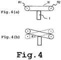
- FIGS. 3A and 3B A 50 mm diameter, 3.5 mm thick, disk-shaped crystal sample 1 in which the (0001) plane serves as the principal plane was prepared, then immobilized on a mount 2 with an epoxy adhesive as shown in FIGS. 3A and 3B .
- FIG. 3A is a front view
- FIG. 3B is a side view.
- a wire saw was furnished for use. The saw was equipped with 70 crystal slicing wires W arranged in parallel, each wire having electrodeposited on the surface thereof diamond abrasive with an average particle size of 12 to 25 ⁇ m. Six of the wires were used for slicing the crystal sample.
- Each of the wires W arranged in parallel was controlled so as to travel by the rotation of a roller R1 and a roller R2 in the same direction, as shown in FIG. 4A , and so as to rock by alternately moving up and down, as shown in FIG. 4B .
- the midpoint of the linear portion of the wire formed between roller R1 and roller R2 is set so as not to rock.
- the maximum swing angle ⁇ of rocking was set to 10°
- the maximum traveling speed by the wire was set to 330 m/min
- the wire rocking frequency was set to 800 times/min.
- the processing damage resistance was measured for the GaN crystal produced in Example 1, and found to be 8.9 J/m 2 .
- the maximum dislocation propagation distance near the center of the GaN crystal substrate produced in Example 1 was measured, and found to be 25.9 ⁇ m.
- a C plane-grown GaN crystal having a thickness of 3.5 mm was obtained by the same method as in (1) above. This crystal was cleaved at the M plane and A plane to 1/4 size, following which 6 hours of heat treatment at 1300°C was carried out by the same method as in (1), giving a crystal with a black-colored surface. This was immersed in 120°C nitric acid (99.9%) to completely remove the gallium metal, thereby giving a crystal sample with cream-colored gallium hydroxide and white gallium oxide remaining on the crystal surface.
- Example 11 In addition to the above heat-treated crystal sample (Example 11), a crystal sample for comparison that had not been heat-treated (Comparative Example 11) was also obtained.
- M plane slice was cut out of each of the crystal samples obtained and the M plane on one side of each sample was chemically polished to a surface state suitable for fluorescent microscopic examination and SEM-CL examination, thereby giving M plane single side-polished samples having a uniform thickness of 3.0 ⁇ 0.05 mm.
- C plane double side-polished samples having a uniform thickness of 1.3 ⁇ 0.05 mm were separately obtained by grinding and polishing at least 500 ⁇ m of the C plane front and back so as to remove the gallium hydroxide layer and gallium oxide layer on the C plane front and back, then chemically polishing to a surface state suitable for SEM-CL examination.
- dislocation aggregates in which basal plane dislocations had gathered were observed at sizes of 10 to 50 ⁇ m in the sample in Example 11 on which heat treatment had been carried out.
- the number of dislocation aggregates present over a surface area of about 0.0054 cm 2 was counted at respective sites 25 mm, 20 mm and 15 mm from the outside edge of the M plane single side-polished sample. To calculate the numerical density of the dislocation aggregates, this number was divided by the surface area of measurement.
- Example 11 One of the dislocation aggregates in the heat-treated sample in Example 11 was examined more closely using a cathodoluminescence scanning electron microscope.
- the cathodoluminescence scanning electron microscope used had a spacial resolution of 3 nm, and the electron beam acceleration voltage was set to 3 kV.
- the incident electron beam was made parallel with the m-axis direction.
- a structure having basal plane dislocations arranged at intervals of from 50 to 500 nm in the c-axis direction was observed over a range of at least 5 ⁇ m in both the c-axis direction and the a-axis direction.
- Dislocation aggregates in the Comparative Example 11 sample that was not subjected to heat treatment were similarly examined using a cathodoluminescence scanning electron microscope. As a result, although these were confirmed to have structures in which the dislocations are arranged at intervals of 50 to 500 nm, the groups had ranges of less than 5 ⁇ m in both the c-axis direction and the a-axis direction.
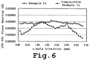
- lattice spacing measurement was carried out by x-ray diffraction analysis in the following manner on the sample from Example 11 that was subjected to heat treatment in (2) above and the sample from Comparative Example 11 that was not subjected to heat treatment.
- the beam was narrowed with a monochromator and a pinhole-type slit, and adjusted so that the Gaussian beam approximation full width at half maximum (FWHM) at the sample surface became 100 ⁇ m in the horizontal direction and 200 ⁇ m in the vertical direction.
- the sample was immobilized on a sample stage so that the c-axis direction was parallel with the horizontal direction.
- 2 ⁇ - ⁇ scans of the (30-30) plane which is the crystal plane parallel to the direction of growth on the production line, were successively carried out at 100 ⁇ m intervals over a length of 3.5 mm along the direction of crystal growth (c-axis direction), and the change in lattice spacing was examined.
- an analyzer crystal and a proportional detector were used on the light-receiving side.
- the temperature within the x-ray unit housing was controlled to within 24.5 ⁇ 1°C, an effort being made to suppress the influence of temperature fluctuations on measurement.
- FIG. 6 The change in lattice spacings on the (30-30) plane at the center of the respective sample substrates in Example 11 and Comparative 11 was measured. The results are shown in FIG. 6 .
- the maximum value d(max), minimum value d(min), average value d(ave) and [d(max) - d(min)]/d(ave) value of the lattice spacings were as shown in Table 3 below.
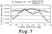
- FIG. 7 shows the results obtained when FIG. 6 was converted into a-axis length change data by multiplying the spacing on the (30-30) plane by 2 ⁇ 3 and converting this to the change in the a-axis length.
- This invention relates to a single-crystal gallium nitride (GaN) substrate which can be used as a substrate for blue light-emitting devices such as blue light-emitting diodes (LED) and blue semiconductor lasers (LD) composed of Group III nitride semiconductors, a method of growing single-crystal gallium nitride substrates (GaN), and a method of producing single-crystal gallium nitride substrates (GaN).
- GaN single-crystal gallium nitride
Landscapes
- Chemical & Material Sciences (AREA)
- Engineering & Computer Science (AREA)
- Crystallography & Structural Chemistry (AREA)
- Materials Engineering (AREA)
- Metallurgy (AREA)
- Organic Chemistry (AREA)
- Physics & Mathematics (AREA)
- Thermal Sciences (AREA)
- Inorganic Chemistry (AREA)
- Condensed Matter Physics & Semiconductors (AREA)
- General Physics & Mathematics (AREA)
- Manufacturing & Machinery (AREA)
- Computer Hardware Design (AREA)
- Microelectronics & Electronic Packaging (AREA)
- Power Engineering (AREA)
- Crystals, And After-Treatments Of Crystals (AREA)
- Recrystallisation Techniques (AREA)
Applications Claiming Priority (3)
| Application Number | Priority Date | Filing Date | Title |
|---|---|---|---|
| JP2011091586 | 2011-04-15 | ||
| JP2011151709A JP2012231103A (ja) | 2011-04-15 | 2011-07-08 | Iii族窒化物結晶の製造方法およびiii族窒化物結晶 |
| PCT/JP2012/060187 WO2012141317A1 (ja) | 2011-04-15 | 2012-04-13 | Iii族窒化物結晶の製造方法およびiii族窒化物結晶 |
Publications (3)
| Publication Number | Publication Date |
|---|---|
| EP2698456A1 EP2698456A1 (en) | 2014-02-19 |
| EP2698456A4 EP2698456A4 (en) | 2014-11-05 |
| EP2698456B1 true EP2698456B1 (en) | 2018-07-25 |
Family
ID=47009475
Family Applications (1)
| Application Number | Title | Priority Date | Filing Date |
|---|---|---|---|
| EP12771993.8A Active EP2698456B1 (en) | 2011-04-15 | 2012-04-13 | Gallium nitride crystal |
Country Status (6)
| Country | Link |
|---|---|
| US (1) | US9502241B2 (enExample) |
| EP (1) | EP2698456B1 (enExample) |
| JP (1) | JP2012231103A (enExample) |
| KR (1) | KR101882541B1 (enExample) |
| CN (1) | CN103502514A (enExample) |
| WO (1) | WO2012141317A1 (enExample) |
Families Citing this family (5)
| Publication number | Priority date | Publication date | Assignee | Title |
|---|---|---|---|---|
| JP5748033B1 (ja) | 2013-08-08 | 2015-07-15 | 三菱化学株式会社 | 自立GaN基板、GaN結晶、GaN単結晶の製造方法および半導体デバイスの製造方法 |
| JP6477501B2 (ja) | 2014-01-17 | 2019-03-06 | 三菱ケミカル株式会社 | GaN基板、GaN基板の製造方法、GaN結晶の製造方法および半導体デバイスの製造方法 |
| WO2015118920A1 (ja) * | 2014-02-07 | 2015-08-13 | 日本碍子株式会社 | 複合基板、発光素子及びそれらの製造方法 |
| CN107574479A (zh) * | 2017-08-14 | 2018-01-12 | 南京大学 | 一种多功能氢化物气相外延生长系统及应用 |
| JP6839694B2 (ja) * | 2018-12-17 | 2021-03-10 | 株式会社デンソー | 酸化ガリウム膜の成膜方法 |
Citations (1)
| Publication number | Priority date | Publication date | Assignee | Title |
|---|---|---|---|---|
| US20070290228A1 (en) * | 2006-06-14 | 2007-12-20 | Hitachi Cable, Ltd. | Nitride semiconductor free-standing substrate |
Family Cites Families (9)
| Publication number | Priority date | Publication date | Assignee | Title |
|---|---|---|---|---|
| US6180270B1 (en) * | 1998-04-24 | 2001-01-30 | The United States Of America As Represented By The Secretary Of The Army | Low defect density gallium nitride epilayer and method of preparing the same |
| JP4618836B2 (ja) * | 2000-01-04 | 2011-01-26 | シャープ株式会社 | 窒化物系化合物半導体基板およびその製造方法 |
| JP4932121B2 (ja) | 2002-03-26 | 2012-05-16 | 日本電気株式会社 | Iii−v族窒化物系半導体基板の製造方法 |
| JP2003327497A (ja) | 2002-05-13 | 2003-11-19 | Sumitomo Electric Ind Ltd | GaN単結晶基板、窒化物系半導体エピタキシャル基板、窒化物系半導体素子及びその製造方法 |
| JP4943132B2 (ja) * | 2005-12-28 | 2012-05-30 | 日本碍子株式会社 | AlN系III族窒化物エピタキシャル膜の転位低減方法 |
| JP4810517B2 (ja) * | 2007-09-10 | 2011-11-09 | 日本電気株式会社 | Iii−v族窒化物系半導体基板 |
| WO2009047894A1 (ja) * | 2007-10-09 | 2009-04-16 | Panasonic Corporation | Iii族窒化物結晶基板の製造方法、iii族窒化物結晶基板、iii族窒化物結晶基板を用いた半導体装置 |
| JP5108641B2 (ja) * | 2008-06-12 | 2012-12-26 | 住友電気工業株式会社 | GaN単結晶基板、窒化物系半導体エピタキシャル基板、及び、窒化物系半導体素子 |
| JP2011006304A (ja) * | 2009-06-29 | 2011-01-13 | Hitachi Cable Ltd | 窒化物半導体基板およびその製造方法 |
-
2011
- 2011-07-08 JP JP2011151709A patent/JP2012231103A/ja not_active Withdrawn
-
2012
- 2012-04-13 KR KR1020137026845A patent/KR101882541B1/ko active Active
- 2012-04-13 CN CN201280018140.0A patent/CN103502514A/zh active Pending
- 2012-04-13 EP EP12771993.8A patent/EP2698456B1/en active Active
- 2012-04-13 WO PCT/JP2012/060187 patent/WO2012141317A1/ja not_active Ceased
-
2013
- 2013-10-15 US US14/054,036 patent/US9502241B2/en active Active
Patent Citations (1)
| Publication number | Priority date | Publication date | Assignee | Title |
|---|---|---|---|---|
| US20070290228A1 (en) * | 2006-06-14 | 2007-12-20 | Hitachi Cable, Ltd. | Nitride semiconductor free-standing substrate |
Also Published As
| Publication number | Publication date |
|---|---|
| WO2012141317A1 (ja) | 2012-10-18 |
| US20140035103A1 (en) | 2014-02-06 |
| EP2698456A1 (en) | 2014-02-19 |
| CN103502514A (zh) | 2014-01-08 |
| KR20140017598A (ko) | 2014-02-11 |
| JP2012231103A (ja) | 2012-11-22 |
| EP2698456A4 (en) | 2014-11-05 |
| US9502241B2 (en) | 2016-11-22 |
| KR101882541B1 (ko) | 2018-07-26 |
Similar Documents
| Publication | Publication Date | Title |
|---|---|---|
| Fujito et al. | Development of bulk GaN crystals and nonpolar/semipolar substrates by HVPE | |
| Bockowski et al. | Challenges and future perspectives in HVPE-GaN growth on ammonothermal GaN seeds | |
| KR101749781B1 (ko) | 단결정 기판, 이를 이용하여 얻어지는 ⅲ족 질화물 결정 및 ⅲ족 질화물 결정의 제조방법 | |
| EP3315639B1 (en) | Self-standing gan substrate, gan crystal, method for producing gan single crystal, and method for producing semiconductor device | |
| Sochacki et al. | Preparation of free-Standing GaN substrates from thick GaN layers crystallized by Hydride Vapor Phase Epitaxy on ammonothermally grown GaN seeds | |
| EP1736574A1 (en) | Nitride crystal, epilayer-containing nitride crystal substrate, semiconductor device and method of manufacturing the same | |
| US10570530B2 (en) | Periodic table group 13 metal nitride crystals and method for manufacturing periodic table group 13 metal nitride crystals | |
| US9502241B2 (en) | Group III nitride crystal production method and group III nitride crystal | |
| KR20130098156A (ko) | GaN계 막의 제조 방법 | |
| EP2264227A1 (en) | Zinc oxide single crystal and method for producing the same | |
| EP1624095A2 (en) | Nitride semiconductor single-crystal substrate and method of its synthesis | |
| JP2013203653A (ja) | Iii族窒化物結晶の製造方法、iii族窒化物結晶およびiii族窒化物結晶基板 | |
| Schowalter et al. | Epitaxial growth of AlN and Al 0.5 Ga 0.5 N layers on aluminum nitride substrates | |
| KR101472832B1 (ko) | Ⅲ-n 층의 생산 방법, ⅲ-n 층 또는 ⅲ-n 기판, 및 이에 기초한 장치 | |
| KR20140074142A (ko) | GaN계 막의 제조 방법 및 그것에 이용되는 복합 기판 | |
| Zhang et al. | Growth of high quality GaN on a novel designed bonding-thinned template by HVPE | |
| Hanser et al. | Growth and fabrication of 2 inch free-standing GaN substrates via the boule growth method | |
| Bliss et al. | Ammonothermal GaN: morphology and properties | |
| JP2013209274A (ja) | 周期表第13族金属窒化物結晶 | |
| JP6103089B2 (ja) | Iii族窒化物結晶の製造方法およびiii族窒化物結晶 | |
| Lantier et al. | Influence of the first preparation steps on the properties of gan layers grown on 6H-SIC by Mbe | |
| JP2013227208A (ja) | Iii族窒化物結晶およびiii族窒化物結晶基板 | |
| Woo et al. | Novel in situ self-separation of a 2 in. free-standing m-plane GaN wafer from an m-plane sapphire substrate by HCl chemical reaction etching in hydride vapor-phase epitaxy | |
| Wang et al. | Epitaxy of single-crystalline GaN films on novel Ca3Ta (Ga0. 5Al0. 5) 3Si2O14 substrates by metal-organic chemical vapor deposition | |
| WO2021064803A1 (ja) | α-Ga2O3系半導体膜 |
Legal Events
| Date | Code | Title | Description |
|---|---|---|---|
| PUAI | Public reference made under article 153(3) epc to a published international application that has entered the european phase |
Free format text: ORIGINAL CODE: 0009012 |
|
| 17P | Request for examination filed |
Effective date: 20131107 |
|
| AK | Designated contracting states |
Kind code of ref document: A1 Designated state(s): AL AT BE BG CH CY CZ DE DK EE ES FI FR GB GR HR HU IE IS IT LI LT LU LV MC MK MT NL NO PL PT RO RS SE SI SK SM TR |
|
| DAX | Request for extension of the european patent (deleted) | ||
| A4 | Supplementary search report drawn up and despatched |
Effective date: 20141007 |
|
| RIC1 | Information provided on ipc code assigned before grant |
Ipc: C30B 33/02 20060101ALI20140930BHEP Ipc: C30B 29/38 20060101AFI20140930BHEP |
|
| RAP1 | Party data changed (applicant data changed or rights of an application transferred) |
Owner name: MITSUBISHI CHEMICAL CORPORATION |
|
| REG | Reference to a national code |
Ref country code: DE Ref legal event code: R079 Ref document number: 602012048898 Country of ref document: DE Free format text: PREVIOUS MAIN CLASS: C30B0029380000 Ipc: C30B0029400000 |
|
| GRAP | Despatch of communication of intention to grant a patent |
Free format text: ORIGINAL CODE: EPIDOSNIGR1 |
|
| STAA | Information on the status of an ep patent application or granted ep patent |
Free format text: STATUS: GRANT OF PATENT IS INTENDED |
|
| RIC1 | Information provided on ipc code assigned before grant |
Ipc: H01L 21/02 20060101ALI20180110BHEP Ipc: H01L 29/20 20060101ALI20180110BHEP Ipc: C30B 29/40 20060101AFI20180110BHEP Ipc: C30B 33/02 20060101ALI20180110BHEP |
|
| INTG | Intention to grant announced |
Effective date: 20180201 |
|
| GRAS | Grant fee paid |
Free format text: ORIGINAL CODE: EPIDOSNIGR3 |
|
| GRAA | (expected) grant |
Free format text: ORIGINAL CODE: 0009210 |
|
| STAA | Information on the status of an ep patent application or granted ep patent |
Free format text: STATUS: THE PATENT HAS BEEN GRANTED |
|
| AK | Designated contracting states |
Kind code of ref document: B1 Designated state(s): AL AT BE BG CH CY CZ DE DK EE ES FI FR GB GR HR HU IE IS IT LI LT LU LV MC MK MT NL NO PL PT RO RS SE SI SK SM TR |
|
| REG | Reference to a national code |
Ref country code: GB Ref legal event code: FG4D |
|
| REG | Reference to a national code |
Ref country code: CH Ref legal event code: EP |
|
| REG | Reference to a national code |
Ref country code: AT Ref legal event code: REF Ref document number: 1021869 Country of ref document: AT Kind code of ref document: T Effective date: 20180815 |
|
| REG | Reference to a national code |
Ref country code: IE Ref legal event code: FG4D |
|
| REG | Reference to a national code |
Ref country code: DE Ref legal event code: R096 Ref document number: 602012048898 Country of ref document: DE |
|
| REG | Reference to a national code |
Ref country code: NL Ref legal event code: MP Effective date: 20180725 |
|
| REG | Reference to a national code |
Ref country code: LT Ref legal event code: MG4D |
|
| PG25 | Lapsed in a contracting state [announced via postgrant information from national office to epo] |
Ref country code: NL Free format text: LAPSE BECAUSE OF FAILURE TO SUBMIT A TRANSLATION OF THE DESCRIPTION OR TO PAY THE FEE WITHIN THE PRESCRIBED TIME-LIMIT Effective date: 20180725 |
|
| REG | Reference to a national code |
Ref country code: AT Ref legal event code: MK05 Ref document number: 1021869 Country of ref document: AT Kind code of ref document: T Effective date: 20180725 |
|
| PG25 | Lapsed in a contracting state [announced via postgrant information from national office to epo] |
Ref country code: LT Free format text: LAPSE BECAUSE OF FAILURE TO SUBMIT A TRANSLATION OF THE DESCRIPTION OR TO PAY THE FEE WITHIN THE PRESCRIBED TIME-LIMIT Effective date: 20180725 Ref country code: FI Free format text: LAPSE BECAUSE OF FAILURE TO SUBMIT A TRANSLATION OF THE DESCRIPTION OR TO PAY THE FEE WITHIN THE PRESCRIBED TIME-LIMIT Effective date: 20180725 Ref country code: RS Free format text: LAPSE BECAUSE OF FAILURE TO SUBMIT A TRANSLATION OF THE DESCRIPTION OR TO PAY THE FEE WITHIN THE PRESCRIBED TIME-LIMIT Effective date: 20180725 Ref country code: IS Free format text: LAPSE BECAUSE OF FAILURE TO SUBMIT A TRANSLATION OF THE DESCRIPTION OR TO PAY THE FEE WITHIN THE PRESCRIBED TIME-LIMIT Effective date: 20181125 Ref country code: AT Free format text: LAPSE BECAUSE OF FAILURE TO SUBMIT A TRANSLATION OF THE DESCRIPTION OR TO PAY THE FEE WITHIN THE PRESCRIBED TIME-LIMIT Effective date: 20180725 Ref country code: NO Free format text: LAPSE BECAUSE OF FAILURE TO SUBMIT A TRANSLATION OF THE DESCRIPTION OR TO PAY THE FEE WITHIN THE PRESCRIBED TIME-LIMIT Effective date: 20181025 Ref country code: BG Free format text: LAPSE BECAUSE OF FAILURE TO SUBMIT A TRANSLATION OF THE DESCRIPTION OR TO PAY THE FEE WITHIN THE PRESCRIBED TIME-LIMIT Effective date: 20181025 Ref country code: GR Free format text: LAPSE BECAUSE OF FAILURE TO SUBMIT A TRANSLATION OF THE DESCRIPTION OR TO PAY THE FEE WITHIN THE PRESCRIBED TIME-LIMIT Effective date: 20181026 Ref country code: SE Free format text: LAPSE BECAUSE OF FAILURE TO SUBMIT A TRANSLATION OF THE DESCRIPTION OR TO PAY THE FEE WITHIN THE PRESCRIBED TIME-LIMIT Effective date: 20180725 Ref country code: PL Free format text: LAPSE BECAUSE OF FAILURE TO SUBMIT A TRANSLATION OF THE DESCRIPTION OR TO PAY THE FEE WITHIN THE PRESCRIBED TIME-LIMIT Effective date: 20180725 |
|
| PG25 | Lapsed in a contracting state [announced via postgrant information from national office to epo] |
Ref country code: AL Free format text: LAPSE BECAUSE OF FAILURE TO SUBMIT A TRANSLATION OF THE DESCRIPTION OR TO PAY THE FEE WITHIN THE PRESCRIBED TIME-LIMIT Effective date: 20180725 Ref country code: LV Free format text: LAPSE BECAUSE OF FAILURE TO SUBMIT A TRANSLATION OF THE DESCRIPTION OR TO PAY THE FEE WITHIN THE PRESCRIBED TIME-LIMIT Effective date: 20180725 Ref country code: HR Free format text: LAPSE BECAUSE OF FAILURE TO SUBMIT A TRANSLATION OF THE DESCRIPTION OR TO PAY THE FEE WITHIN THE PRESCRIBED TIME-LIMIT Effective date: 20180725 |
|
| REG | Reference to a national code |
Ref country code: DE Ref legal event code: R097 Ref document number: 602012048898 Country of ref document: DE |
|
| PG25 | Lapsed in a contracting state [announced via postgrant information from national office to epo] |
Ref country code: CZ Free format text: LAPSE BECAUSE OF FAILURE TO SUBMIT A TRANSLATION OF THE DESCRIPTION OR TO PAY THE FEE WITHIN THE PRESCRIBED TIME-LIMIT Effective date: 20180725 Ref country code: ES Free format text: LAPSE BECAUSE OF FAILURE TO SUBMIT A TRANSLATION OF THE DESCRIPTION OR TO PAY THE FEE WITHIN THE PRESCRIBED TIME-LIMIT Effective date: 20180725 Ref country code: EE Free format text: LAPSE BECAUSE OF FAILURE TO SUBMIT A TRANSLATION OF THE DESCRIPTION OR TO PAY THE FEE WITHIN THE PRESCRIBED TIME-LIMIT Effective date: 20180725 Ref country code: RO Free format text: LAPSE BECAUSE OF FAILURE TO SUBMIT A TRANSLATION OF THE DESCRIPTION OR TO PAY THE FEE WITHIN THE PRESCRIBED TIME-LIMIT Effective date: 20180725 Ref country code: IT Free format text: LAPSE BECAUSE OF FAILURE TO SUBMIT A TRANSLATION OF THE DESCRIPTION OR TO PAY THE FEE WITHIN THE PRESCRIBED TIME-LIMIT Effective date: 20180725 |
|
| PG25 | Lapsed in a contracting state [announced via postgrant information from national office to epo] |
Ref country code: DK Free format text: LAPSE BECAUSE OF FAILURE TO SUBMIT A TRANSLATION OF THE DESCRIPTION OR TO PAY THE FEE WITHIN THE PRESCRIBED TIME-LIMIT Effective date: 20180725 Ref country code: SM Free format text: LAPSE BECAUSE OF FAILURE TO SUBMIT A TRANSLATION OF THE DESCRIPTION OR TO PAY THE FEE WITHIN THE PRESCRIBED TIME-LIMIT Effective date: 20180725 Ref country code: SK Free format text: LAPSE BECAUSE OF FAILURE TO SUBMIT A TRANSLATION OF THE DESCRIPTION OR TO PAY THE FEE WITHIN THE PRESCRIBED TIME-LIMIT Effective date: 20180725 |
|
| PLBE | No opposition filed within time limit |
Free format text: ORIGINAL CODE: 0009261 |
|
| STAA | Information on the status of an ep patent application or granted ep patent |
Free format text: STATUS: NO OPPOSITION FILED WITHIN TIME LIMIT |
|
| 26N | No opposition filed |
Effective date: 20190426 |
|
| PG25 | Lapsed in a contracting state [announced via postgrant information from national office to epo] |
Ref country code: SI Free format text: LAPSE BECAUSE OF FAILURE TO SUBMIT A TRANSLATION OF THE DESCRIPTION OR TO PAY THE FEE WITHIN THE PRESCRIBED TIME-LIMIT Effective date: 20180725 |
|
| REG | Reference to a national code |
Ref country code: CH Ref legal event code: PL |
|
| REG | Reference to a national code |
Ref country code: BE Ref legal event code: MM Effective date: 20190430 |
|
| GBPC | Gb: european patent ceased through non-payment of renewal fee |
Effective date: 20190413 |
|
| PG25 | Lapsed in a contracting state [announced via postgrant information from national office to epo] |
Ref country code: LU Free format text: LAPSE BECAUSE OF NON-PAYMENT OF DUE FEES Effective date: 20190413 Ref country code: MC Free format text: LAPSE BECAUSE OF FAILURE TO SUBMIT A TRANSLATION OF THE DESCRIPTION OR TO PAY THE FEE WITHIN THE PRESCRIBED TIME-LIMIT Effective date: 20180725 |
|
| PG25 | Lapsed in a contracting state [announced via postgrant information from national office to epo] |
Ref country code: CH Free format text: LAPSE BECAUSE OF NON-PAYMENT OF DUE FEES Effective date: 20190430 Ref country code: GB Free format text: LAPSE BECAUSE OF NON-PAYMENT OF DUE FEES Effective date: 20190413 Ref country code: LI Free format text: LAPSE BECAUSE OF NON-PAYMENT OF DUE FEES Effective date: 20190430 |
|
| PG25 | Lapsed in a contracting state [announced via postgrant information from national office to epo] |
Ref country code: BE Free format text: LAPSE BECAUSE OF NON-PAYMENT OF DUE FEES Effective date: 20190430 |
|
| PG25 | Lapsed in a contracting state [announced via postgrant information from national office to epo] |
Ref country code: TR Free format text: LAPSE BECAUSE OF FAILURE TO SUBMIT A TRANSLATION OF THE DESCRIPTION OR TO PAY THE FEE WITHIN THE PRESCRIBED TIME-LIMIT Effective date: 20180725 |
|
| PG25 | Lapsed in a contracting state [announced via postgrant information from national office to epo] |
Ref country code: IE Free format text: LAPSE BECAUSE OF NON-PAYMENT OF DUE FEES Effective date: 20190413 |
|
| PG25 | Lapsed in a contracting state [announced via postgrant information from national office to epo] |
Ref country code: PT Free format text: LAPSE BECAUSE OF FAILURE TO SUBMIT A TRANSLATION OF THE DESCRIPTION OR TO PAY THE FEE WITHIN THE PRESCRIBED TIME-LIMIT Effective date: 20181125 |
|
| PG25 | Lapsed in a contracting state [announced via postgrant information from national office to epo] |
Ref country code: CY Free format text: LAPSE BECAUSE OF FAILURE TO SUBMIT A TRANSLATION OF THE DESCRIPTION OR TO PAY THE FEE WITHIN THE PRESCRIBED TIME-LIMIT Effective date: 20180725 |
|
| PG25 | Lapsed in a contracting state [announced via postgrant information from national office to epo] |
Ref country code: MT Free format text: LAPSE BECAUSE OF FAILURE TO SUBMIT A TRANSLATION OF THE DESCRIPTION OR TO PAY THE FEE WITHIN THE PRESCRIBED TIME-LIMIT Effective date: 20180725 Ref country code: HU Free format text: LAPSE BECAUSE OF FAILURE TO SUBMIT A TRANSLATION OF THE DESCRIPTION OR TO PAY THE FEE WITHIN THE PRESCRIBED TIME-LIMIT; INVALID AB INITIO Effective date: 20120413 |
|
| PG25 | Lapsed in a contracting state [announced via postgrant information from national office to epo] |
Ref country code: MK Free format text: LAPSE BECAUSE OF FAILURE TO SUBMIT A TRANSLATION OF THE DESCRIPTION OR TO PAY THE FEE WITHIN THE PRESCRIBED TIME-LIMIT Effective date: 20180725 |
|
| P01 | Opt-out of the competence of the unified patent court (upc) registered |
Effective date: 20230522 |
|
| PGFP | Annual fee paid to national office [announced via postgrant information from national office to epo] |
Ref country code: FR Payment date: 20250310 Year of fee payment: 14 |
|
| PGFP | Annual fee paid to national office [announced via postgrant information from national office to epo] |
Ref country code: DE Payment date: 20250305 Year of fee payment: 14 |