EP2672479B1 - Unité de commande de grille sur réseau, circuit de commande de grille sur réseau et dispositif d'affichage - Google Patents
Unité de commande de grille sur réseau, circuit de commande de grille sur réseau et dispositif d'affichage Download PDFInfo
- Publication number
- EP2672479B1 EP2672479B1 EP12830911.9A EP12830911A EP2672479B1 EP 2672479 B1 EP2672479 B1 EP 2672479B1 EP 12830911 A EP12830911 A EP 12830911A EP 2672479 B1 EP2672479 B1 EP 2672479B1
- Authority
- EP
- European Patent Office
- Prior art keywords
- thin film
- film transistor
- gate
- array substrate
- substrate row
- Prior art date
- Legal status (The legal status is an assumption and is not a legal conclusion. Google has not performed a legal analysis and makes no representation as to the accuracy of the status listed.)
- Active
Links
- 239000010409 thin film Substances 0.000 claims description 135
- 239000000758 substrate Substances 0.000 claims description 111
- 239000003990 capacitor Substances 0.000 claims description 13
- 229920001621 AMOLED Polymers 0.000 claims description 11
- 238000000034 method Methods 0.000 claims description 10
- 102100040844 Dual specificity protein kinase CLK2 Human genes 0.000 description 7
- 101000749291 Homo sapiens Dual specificity protein kinase CLK2 Proteins 0.000 description 7
- 238000010586 diagram Methods 0.000 description 6
- 102100040862 Dual specificity protein kinase CLK1 Human genes 0.000 description 4
- 101000749294 Homo sapiens Dual specificity protein kinase CLK1 Proteins 0.000 description 4
- 239000004973 liquid crystal related substance Substances 0.000 description 4
- 239000011159 matrix material Substances 0.000 description 4
- 238000005070 sampling Methods 0.000 description 3
- 229910021420 polycrystalline silicon Inorganic materials 0.000 description 2
- 229920005591 polysilicon Polymers 0.000 description 2
- 230000001447 compensatory effect Effects 0.000 description 1
- 230000000415 inactivating effect Effects 0.000 description 1
- 230000010354 integration Effects 0.000 description 1
- 230000000670 limiting effect Effects 0.000 description 1
- 239000000463 material Substances 0.000 description 1
- 230000000750 progressive effect Effects 0.000 description 1
- 230000001052 transient effect Effects 0.000 description 1
Images

Classifications
-
- G—PHYSICS
- G09—EDUCATION; CRYPTOGRAPHY; DISPLAY; ADVERTISING; SEALS
- G09G—ARRANGEMENTS OR CIRCUITS FOR CONTROL OF INDICATING DEVICES USING STATIC MEANS TO PRESENT VARIABLE INFORMATION
- G09G3/00—Control arrangements or circuits, of interest only in connection with visual indicators other than cathode-ray tubes
- G09G3/20—Control arrangements or circuits, of interest only in connection with visual indicators other than cathode-ray tubes for presentation of an assembly of a number of characters, e.g. a page, by composing the assembly by combination of individual elements arranged in a matrix no fixed position being assigned to or needed to be assigned to the individual characters or partial characters
- G09G3/22—Control arrangements or circuits, of interest only in connection with visual indicators other than cathode-ray tubes for presentation of an assembly of a number of characters, e.g. a page, by composing the assembly by combination of individual elements arranged in a matrix no fixed position being assigned to or needed to be assigned to the individual characters or partial characters using controlled light sources
- G09G3/30—Control arrangements or circuits, of interest only in connection with visual indicators other than cathode-ray tubes for presentation of an assembly of a number of characters, e.g. a page, by composing the assembly by combination of individual elements arranged in a matrix no fixed position being assigned to or needed to be assigned to the individual characters or partial characters using controlled light sources using electroluminescent panels
- G09G3/32—Control arrangements or circuits, of interest only in connection with visual indicators other than cathode-ray tubes for presentation of an assembly of a number of characters, e.g. a page, by composing the assembly by combination of individual elements arranged in a matrix no fixed position being assigned to or needed to be assigned to the individual characters or partial characters using controlled light sources using electroluminescent panels semiconductive, e.g. using light-emitting diodes [LED]
- G09G3/3208—Control arrangements or circuits, of interest only in connection with visual indicators other than cathode-ray tubes for presentation of an assembly of a number of characters, e.g. a page, by composing the assembly by combination of individual elements arranged in a matrix no fixed position being assigned to or needed to be assigned to the individual characters or partial characters using controlled light sources using electroluminescent panels semiconductive, e.g. using light-emitting diodes [LED] organic, e.g. using organic light-emitting diodes [OLED]
- G09G3/3225—Control arrangements or circuits, of interest only in connection with visual indicators other than cathode-ray tubes for presentation of an assembly of a number of characters, e.g. a page, by composing the assembly by combination of individual elements arranged in a matrix no fixed position being assigned to or needed to be assigned to the individual characters or partial characters using controlled light sources using electroluminescent panels semiconductive, e.g. using light-emitting diodes [LED] organic, e.g. using organic light-emitting diodes [OLED] using an active matrix
-
- G—PHYSICS
- G09—EDUCATION; CRYPTOGRAPHY; DISPLAY; ADVERTISING; SEALS
- G09G—ARRANGEMENTS OR CIRCUITS FOR CONTROL OF INDICATING DEVICES USING STATIC MEANS TO PRESENT VARIABLE INFORMATION
- G09G3/00—Control arrangements or circuits, of interest only in connection with visual indicators other than cathode-ray tubes
- G09G3/20—Control arrangements or circuits, of interest only in connection with visual indicators other than cathode-ray tubes for presentation of an assembly of a number of characters, e.g. a page, by composing the assembly by combination of individual elements arranged in a matrix no fixed position being assigned to or needed to be assigned to the individual characters or partial characters
- G09G3/22—Control arrangements or circuits, of interest only in connection with visual indicators other than cathode-ray tubes for presentation of an assembly of a number of characters, e.g. a page, by composing the assembly by combination of individual elements arranged in a matrix no fixed position being assigned to or needed to be assigned to the individual characters or partial characters using controlled light sources
- G09G3/30—Control arrangements or circuits, of interest only in connection with visual indicators other than cathode-ray tubes for presentation of an assembly of a number of characters, e.g. a page, by composing the assembly by combination of individual elements arranged in a matrix no fixed position being assigned to or needed to be assigned to the individual characters or partial characters using controlled light sources using electroluminescent panels
- G09G3/32—Control arrangements or circuits, of interest only in connection with visual indicators other than cathode-ray tubes for presentation of an assembly of a number of characters, e.g. a page, by composing the assembly by combination of individual elements arranged in a matrix no fixed position being assigned to or needed to be assigned to the individual characters or partial characters using controlled light sources using electroluminescent panels semiconductive, e.g. using light-emitting diodes [LED]
- G09G3/3208—Control arrangements or circuits, of interest only in connection with visual indicators other than cathode-ray tubes for presentation of an assembly of a number of characters, e.g. a page, by composing the assembly by combination of individual elements arranged in a matrix no fixed position being assigned to or needed to be assigned to the individual characters or partial characters using controlled light sources using electroluminescent panels semiconductive, e.g. using light-emitting diodes [LED] organic, e.g. using organic light-emitting diodes [OLED]
- G09G3/3266—Details of drivers for scan electrodes
-
- G—PHYSICS
- G11—INFORMATION STORAGE
- G11C—STATIC STORES
- G11C19/00—Digital stores in which the information is moved stepwise, e.g. shift registers
- G11C19/28—Digital stores in which the information is moved stepwise, e.g. shift registers using semiconductor elements
-
- G—PHYSICS
- G09—EDUCATION; CRYPTOGRAPHY; DISPLAY; ADVERTISING; SEALS
- G09G—ARRANGEMENTS OR CIRCUITS FOR CONTROL OF INDICATING DEVICES USING STATIC MEANS TO PRESENT VARIABLE INFORMATION
- G09G2300/00—Aspects of the constitution of display devices
- G09G2300/08—Active matrix structure, i.e. with use of active elements, inclusive of non-linear two terminal elements, in the pixels together with light emitting or modulating elements
- G09G2300/0809—Several active elements per pixel in active matrix panels
- G09G2300/0842—Several active elements per pixel in active matrix panels forming a memory circuit, e.g. a dynamic memory with one capacitor
- G09G2300/0861—Several active elements per pixel in active matrix panels forming a memory circuit, e.g. a dynamic memory with one capacitor with additional control of the display period without amending the charge stored in a pixel memory, e.g. by means of additional select electrodes
Definitions
- the present invention relates to the field of organic light-emitting display, and more particularly relates to an array substrate row driving unit, array substrate row driving circuit and a display device.
- the organic light-emitting diode has been increasingly used in high - performance display due to its advantages of high brightness, wide viewing angle and rapid response speed, etc.
- the conventional passive matrix organic light-emitting diode display requires a shorter driving time of a single pixel, which needs to increase the transient current, thus increasing the power consumption.
- the application of a large current will cause the voltage drop on the ITO (pixel electrode) line to be excessively large and the working voltage of OLED to be too high, thereby reducing its efficiency.
- the active matrix organic light-emitting diode display inputs OLED current by progressive scanning via switch transistors, which can solve these problems very well.
- the array substrate row driving circuit integrates the gate switch circuit on an array substrate, thus achieving a high-degree integration of the driving circuit, reducing costs both by saving material and reducing process steps.
- AMOLED active matrix organic light - emitting diode
- the state control signal of the organic light-emitting display diodes for an AMOLED display backplane constituted of the P-type transistors is a positive level signal to ensure that an OLED component is in an OFF state during the process of writing display data into the pixel units, while after the display data have been written into the pixel units, the OLED component turns on and emits light so as to ensure that the displaying image will not flicker due to the unstable state of the pixel circuit when the data are being written.
- EP 1 843 317 A1 discloses a scan driving circuit for a OLED display with a first scan driver including a plurality of first units, the first units receiving an input signal or an output voltage of a previous first unit and first and second clock signals to output a scan signal, and a second scan driver having a plurality of second units, the second units receiving a plurality of scan signals output from respective ones of the first units, and at least one of the first and second clock signals, and outputting an emission control signal.
- US 2011/012823 A1 discloses a liquid crystal display and a shift register device thereof, which shift register device includes a plurality of shift registers connected in series.
- US 2006/001637 A1 discloses a display device including a display panel having gate lines, data lines, display members, and switching members; a timing controller configured to output image data, gate control signals, and data control signals; a shift register configured to sequentially output gate signals to the gate lines based on the gate control signals; and a data drive circuit configured to output data signals to the data lines based on the data control signals, wherein the shift register includes stages corresponding to the gate lines, each of the stages outputting a first clock signal as the gate signal to a corresponding gate line in response to the gate signal of an adjacent stage, inactivating the gate line in response to a second clock signal. An inactive state of the gate line may be maintained in correspondence with the first clock signal.
- AMOLED active matrix organic light-emitting diode
- AMLCD Active Matrix Liquid Crystal Display
- AMOLED active matrix organic light-emitting diode
- the pixel circuit of the AMOLED often requires a corresponding compensative structure, so the structure of the pixel circuit of the AMOLED is more complex, and correspondingly needs to occupy a larger circuit layout area.
- An embodiment of the present invention provides an array substrate row driving circuit, which has a simple structure and stable performance, for the active matrix organic light-emitting display, and the array substrate row driving circuit comprises a plurality of cascading array substrate row driving units manufactured on the array substrate of a liquid crystal through an array film-forming process.
- Each array substrate row driving unit contains 8 thin film transistors and 2 capacitors.
- the array substrate row driving unit is divided into two stages, a first stage being used for generating a the conventional gate line strobe signal, a second stage being used for accordingly generating a control signal to control the switching of the organic light-emitting diode.
- the array substrate row driving circuit according to an embodiment of present invention has a simple and compact structure, which reduces the circuit layout area, and is the best choice to achieve high resolution AMOLED display.
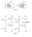
- the array substrate row driving unit includes a gate driving module 11 and an emission control module 12, wherein,
- the gate driving module 11 being connected to the emission control module 12, for generating a gate driving signal
- the emission control module being is used for generating an emission control signal for controlling the switching of OLED under control of the gate driving signal, the gate driving signal having an opposite phase to that of the emission control signal.
- the emission control module 12 In the array substrate row driving unit according to the first embodiment of the present invention, the emission control module 12 generates an emission control signal that has an opposite phase to that of the gate drive signal, so that OLED component is in an OFF state during the process of writing the display data into the pixel units, while OLED component turns on and emits light after the display data have been written into the pixel units, therefore ensuring that the displaying image will not flicker due to the unstable state of the pixel circuit when the data is written.
- FIG. 2 it shows a circuit diagram of an array substrate row driving unit according to a second embodiment of the present invention.
- the array substrate row driving unit according to the second embodiment of the present invention is based on that of the first embodiment of the present invention.
- the array substrate row driving unit according to the second embodiment of the present invention is based on that of the first embodiment of the present invention.
- the gate driving module including a first thin film transistor T1, a second thin film transistor T2, a third thin film transistor T3, a fourth thin film transistor T4 and a first bootstrap capacitor C1, wherein,
- the first thin film transistor T1 having a gate connected to the output for the gate driving signal of the previous-stage array substrate row driving unit, a source connected to a drain of the second thin film transistor T2, and a drain connected to the low-level output of the driving power supply;
- the second thin film transistor T2 having gate connected to the output for the gate driving signal of next-stage array substrate row driving unit, and a source connected to the high-level output of the driving power supply;
- the third thin film transistor T3 having a gate connected to the source of the first thin film transistor T1, a source connected to a drain of the fourth thin film transistor T4, and a drain connected to the input for a first clock signal;
- the fourth thin film transistor T4 having a gate connected to the input for a second clock signal, and a source connected to the high-level output of the driving power supply;
- the first bootstrap capacitor C1 being connected between the gate and source of the third thin film transistor T3;
- the first thin film transistor T1, the second thin film transistor T2, the third thin film transistor T3 and the fourth thin film transistor T4 being p-type thin film transistors.
- the emission control module comprising a fifth thin film transistor T5, a sixth fifth thin film transistor T6, a seventh thin film transistor T7, an eighth thin film transistor T8 and a second bootstrap capacitor C2, wherein,
- the fifth thin film transistor T5 having a gate connected to the output for the gate driving signal of next-stage array substrate row driving unit, a source connected to the drain of the sixth thin film transistor T6, and a drain connected to the low-level output of the driving power supply;
- the sixth thin film transistor T6 having a gate connected to the drain of the fourth thin film transistor T4, and a source connected to the high-level output of the driving power supply;
- the seventh thin film transistor T7 having a gate connected to the source of the fifth thin film transistor T5, a source connected to a drain of the eighth thin film transistor T8, and a drain connected to the low-level output of the driving power supply;
- the eighth thin film transistor T8 having a gate connected to the gate of the sixth thin film transistor T6, and a source connected to the high-level output of the driving power supply;
- the second bootstrap capacitor C2 being connected between the gate and source of the seventh thin film transistor T7;
- the fifth thin film transistor T5, the sixth thin film transistor T6, the seventh thin film transistor T7 and the eighth thin film transistor T8 being p-type thin film transistors;
- the gate of the first thin film transistor T1 being the input of the array substrate row driving unit according to the second embodiment of present invention
- the gate of the second thin film transistor T2 being the reset terminal of the array substrate row driving unit according to the second embodiment of present invention
- the source of the third thin film transistor T3 being the output for the gate driving signal of the array substrate row driving unit according to the second embodiment of present invention
- the source of the seventh thin film transistor T7 being an output for the emission control signal of the array substrate row driving unit according to the second embodiment of present invention.
- output voltage of the low-level output of the driving power supply is VGL
- output voltage of the high-level output of the driving power supply is VGH
- a first clock signal CLK1 is input into the first clock signal input
- a second clock signal CLK2 is input into the second clock signal input.
- the output signal of the output for the gate driving signal of the previous-stage array substrate row driving unit is G[n-1], that of the present-stage array substrate row driving unit is G[n], and that of the next-stage array substrate row driving unit is G[n+1].
- the output signal of the output for the emission control signal of the present-stage array substrate row driving unit is EMISSION[n].
- the point N1 is a node connected to the gate of the third thin film transistor T3, and the point N2 is a node connected to the gate of the seventh thin film transistor T7.
- the array substrate row driving unit according to the second embodiment of the present invention is controlled by the first clock signal CLK1 and the second clock signal CLK2.
- the output signal of the output for the gate driving signal of the previous-stage array substrate row driving unit G[n-1] serves as the input signal of the present-stage array substrate row driving unit
- the output signal of the output for the gate driving signal of the next-stage array substrate row driving unit G[n+1] serves as the reset signal of the present-stage array substrate row driving unit.
- the work process of the array substrate row driving unit according to the second embodiment of the present invention is divided into input sampling phase t1, signal output phase t2 and reset phase T3.
- G[n-1] is low and T1 is turned on, while G[n+1] is high and T2 is turned off, so in this case the potential at point N1 is correspondingly pulled down to VGL+
- CLK2 is low, T4 is turned off, and G[n] is high, so at this time C1 is being charged, and the input signal is sampled.
- G[n] and G [n+1] are both high, ensuring the working state of each transistor included in the control module will not change.
- G[n-1] and G[n+1] are both high, and the potential at point N1 is maintained a VGL+
- CLK2 is high, T4 is turned off and G[n] is low, so T6 and T8 are turned on.
- EMISSION[n] is high, used for lighting the organic light-emitting diode components.
- G [n -1] is high, ensuring that transistors T1 and T3 are turned off; CLK2 is low and T4 is turned on, so G[n] is pulled up to a high level; G[N] is high, ensuring that T6 and T8 are turned off, while G[n+1] is low, and the voltage at point N1 is pulled up again by turning on T2; T5 is turned on at the same time, and the potential at point N2 is pulled down to VGL+
- Figure 4 shows the circuit diagram of the array substrate row driving unit according to a third embodiment of the present invention.
- the array substrate row driving unit according to the third embodiment of the present invention is based on that according to the first embodiment of the present invention.
- the gate driving module comprises a first thin film transistor T1, a second thin film transistor T2, a third thin film transistor T3, a fourth thin film transistor T4 and a first bootstrap capacitor C1, wherein, the first thin film transistor T1, having a gate connected to the output for the gate driving signal of the previous-stage array substrate row driving unit, a source connected to a drain of the second thin film transistor T2, and a drain connected to the high-level output of the driving power supply; the second thin film transistor T2, having a gate connected to the output for the gate driving signal of the next-stage array substrate row driving unit, and a source connected to the low-level output of the driving power supply; the third thin film transistor T3, having a gate connected to the source of the first thin film transistor T1,
- the array substrate row driving unit according to the third embodiment of the present invention is controlled by the first clock signal CLK1 and the second clock signal CLK2.
- the output signal of the output for the gate driving signal of the previous-stage array substrate row driving unit G[n-1] serves as the input signal of the present-stage array substrate row driving unit
- the output signal of the output for the gate driving signal of the next-stage array substrate row driving unit G[n+1] serves as the reset signal of the present-stage array substrate row driving unit.
- the work process of the array substrate row driving unit according to the third embodiment of the present invention is divided into input sampling phase t1, signal output phase t2 and reset phase T3.
- the work process of the third embodiment of the present invention is similar to the second embodiment, and the related description will be omitted hereinafter.
- the exemplary emission control module of the array substrate row driving unit according to the second and the third embodiment of the present invention are only by way of illustration, and have no limiting effect on the structure of the emission control module. Any control components that can generate, under control of the gate driving signal, an emission control signal which control the switching of the organic light-emitting diode and which has an opposite phase to that of the gate driving signal can all be used for constituting the emission control module.
- An embodiment of the present invention also provides an array substrate row driving circuit, including multi-stages aforementioned array substrate row driving units manufactured on the array substrate of a liquid crystal through an array film-forming process.
- the input of each stage of the array substrate row driving units is connected to the output for the gate driving signal of the previous-stage array substrate row driving unit;
- the reset terminal of each stage of the array substrate row driving units is connected to the output for the gate driving signal of the next-stage array substrate row driving unit.
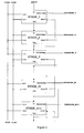
- Fig. 6 shows an array substrate row driving circuit according to an embodiment of the present invention, comprising N+1 stages of array substrate row driving units, wherein N being a positive integer.
- the input of the first-stage array substrate row driving unit is connected to the input signal INPUT.
- the input of each stage of the array substrate row driving units IN is connected to the output for the gate driving signal of the previous-stage array substrate row driving unit.
- the reset terminal of each stage of the array substrate row driving units RESET is connected to the output for the gate driving signal of the next-stage array substrate row driving unit.
- EMISSION_1, EMISSION _2, EMISSION _3, EMISSION _N and EMISSION _N +1 indicate the output for the emission control signal of the first-stage array substrate row driving unit, the output for the emission control signal of the second-stage array substrate row driving unit, the output for the emission control signal of the third-stage array substrate row driving unit, the output for the emission control signal of the Nth-stage array substrate row driving unit and the output for the emission control signal of the N+1th-stage array substrate row driving unit respectively.
- STAGE_1, STAGE _2, STAGE _3, STAGE _N and STAGE _N +1 indicate the first-stage array substrate row driving unit, the second-stage array substrate row driving unit, the third-stage array substrate row driving unit, the Nth-stage array substrate row driving unit and the N+1 th-stage array substrate row driving unit.
- An embodiment of the present invention also provides a display device, comprising the aforementioned array substrate row driving circuit.
Landscapes
- Engineering & Computer Science (AREA)
- Physics & Mathematics (AREA)
- Computer Hardware Design (AREA)
- General Physics & Mathematics (AREA)
- Theoretical Computer Science (AREA)
- Control Of Indicators Other Than Cathode Ray Tubes (AREA)
- Electroluminescent Light Sources (AREA)
- Control Of El Displays (AREA)
Claims (7)
- Circuit de commande de ligne pour substrat de matrice destiné à un affichage AMOLED, comprenant plusieurs étages d'unités de commande de ligne pour substrat de matrice, dans lequel une unité de commande de ligne pour substrat de matrice d'étage actuel comprend un module de commande de grille (11) destiné à générer et émettre un signal de commande de grille (G[n]) et un module de contrôle d'émission (12) destiné à générer et émettre un signal de contrôle d'émission (EMISSION [n]) ;
dans lequel le module de contrôle d'émission (12) est connecté à la sortie pour le signal de commande de grille (G[n]) du module de commande de grille (11), et le signal de contrôle d'émission est destiné à contrôler la commutation d'une OLED sous le contrôle du signal de commande de grille, le signal de commande de grille présentant une phase opposée à celle du signal de contrôle d'émission ;
caractérisé par fait que le module de commande de grille (11) comprend un premier transistor à couches minces (T1), un deuxième transistor à couches minces (T2), un troisième transistor à couches minces (T3), un quatrième transistor à couches minces (T4) et un premier condensateur d'amorçage (C1), dans lequel
le premier transistor à couches minces (T1) présente une grille connectée à la sortie pour le signal de commande de grille G[n-1] de l'unité de commande de ligne pour substrat de matrice d'étage précédent, une source connectée à un drain du deuxième transistor à couches minces (T2), et un drain connecté à une sortie de premier niveau de l'alimentation électrique de commande ;
le deuxième transistor à couches minces (T2) présente une grille connectée à la sortie pour le signal de commande de grille (G[n+1]) de l'unité de commande de ligne pour substrat de matrice d'étage suivant, et une source connectée à une sortie de second niveau de l'alimentation électrique de commande ;
le troisième transistor à couches minces (T3) présente une grille connectée à la source du premier transistor à couches minces (T1), une source connectée à un drain du quatrième transistor à couches minces (T4), et un drain connecté à l'entrée pour un premier signal d'horloge (CLK1) ;
le quatrième transistor à couches minces (T4) présente une grille connectée à l'entrée pour un second signal d'horloge (CLK2), et une source connectée à la sortie de second niveau de l'alimentation électrique de commande ;
le premier condensateur d'amorçage (C1) est connecté entre la grille et la source du troisième transistor à couches minces (T3) ;
la grille du premier transistor à couches minces (T1) est une entrée, et la source du troisième transistor à couches minces (T3) est la sortie pour le signal de commande de grille (G[n]) du module de contrôle de grille (11), et
caractérisé en outre par fait que le module de contrôle d'émission (12) comprend un cinquième transistor à couches minces (T5), un sixième transistor à couches minces (T6), un septième transistor à couches minces (T7), un huitième transistor à couches minces (T8), et un second condensateur d'amorçage (C2), dans lequel
le cinquième transistor à couches minces (T5) présente une grille connectée à la sortie pour le signal de commande de grille (G[n+1]) de l'unité de commande de ligne pour substrat de matrice d'étage suivant, une source connectée à un drain du sixième transistor à couches minces (T6), et un drain connecté au premier niveau de sortie de l'alimentation électrique de commande ;
le sixième transistor à couches minces (T6) présente une grille connectée au drain du quatrième transistor à couches minces (T4), et une source connectée au second niveau de sortie de l'alimentation électrique de commande ;
le septième transistor à couches minces (T7) présente une grille connectée à la source du cinquième transistor à couches minces (T5), une source connectée à un drain du huitième transistor à couches minces (T8), et un drain connecté au premier niveau de sortie de l'alimentation électrique de commande ;
le huitième transistor à couches minces (T8) présente une grille connectée à la grille du sixième transistor à couches minces (T6), et une source connectée au second niveau de sortie de l'alimentation électrique de commande ;
le second condensateur d'amorçage (C2) est connecté entre la grille et la source du septième transistor à couches minces (T7), et
la source du septième transistor à couches minces (T7) est la sortie pour le signal de contrôle d'émission (EMISSION[n]). - Circuit de commande de ligne pour substrat de matrice selon la revendication 1, dans lequel
la sortie de premier niveau de l'alimentation électrique de commande est une sortie de niveau bas ;
la sortie de second niveau de l'alimentation électrique de commande est une sortie de niveau haut, et
le premier transistor à couches minces (T1), le deuxième transistor à couches minces (T2), le troisième transistor à couches minces (T3), et le quatrième transistor à couches minces (T4) sont des transistors à couches minces de type p. - Circuit de commande de ligne pour substrat de matrice selon la revendication 2, dans lequel
la sortie de premier niveau de l'alimentation électrique de commande est une sortie de niveau bas ;
la sortie de second niveau de l'alimentation électrique de commande est une sortie de niveau haut, et
le cinquième transistor à couches minces (T5), le sixième transistor à couches minces (T6), le septième transistor à couches minces (T7), et le huitième transistor à couches minces (T8) sont des transistors à couches minces de type p. - Circuit de commande de ligne pour substrat de matrice selon la revendication 1, dans lequel
la sortie de premier niveau de l'alimentation électrique de commande est une sortie de niveau haut ;
la sortie de second niveau de l'alimentation électrique de commande est une sortie de niveau bas, et
le premier transistor à couches minces (T1), le deuxième transistor à couches minces (T2), le troisième transistor à couches minces (T3), et le quatrième transistor à couches minces (T4) sont des transistors à couches minces de type n. - Circuit de commande de ligne pour substrat de matrice selon la revendication 4, dans lequel
la sortie de premier niveau de l'alimentation électrique de commande est une sortie de niveau haut ;
la sortie de second niveau de l'alimentation électrique de commande est une sortie de niveau bas, et
le cinquième transistor à couches minces (T5), le sixième transistor à couches minces (T6), le septième transistor à couches minces (T7), et le huitième transistor à couches minces (T8) sont des transistors à couches minces de type n. - Circuit de commande de ligne pour substrat de matrice selon l'une quelconque des revendications 1 à 5, dans lequel le circuit de commande de ligne pour substrat de matrice est fabriqué sur le substrat de matrice d'un affichage à diode électroluminescente organique par le biais d'un processus de formation de couche de matrice, dans lequel
à l'exception de l'unité de commande de ligne pour substrat de matrice de premier étage, une entrée de chaque étage des unités de commande de ligne pour substrat de matrice est connectée à la sortie pour le signal de commande de grille de l'unité de commande de ligne pour substrat de matrice d'étage précédent, et
à l'exception de l'unité de commande de ligne pour substrat de matrice d'étage final, une borne de réinitialisation de chaque étage des unités de commande de ligne pour substrat de matrice est connectée à la sortie pour le signal de commande de grille de l'unité de commande de ligne pour substrat de matrice d'étage suivant adjacente à l'unité de commande de ligne pour substrat de matrice d'étage actuel. - Dispositif d'affichage comprenant le circuit de commande de ligne pour substrat de matrice selon la revendication 6.
Applications Claiming Priority (2)
| Application Number | Priority Date | Filing Date | Title |
|---|---|---|---|
| CN201210050062.4A CN102708795B (zh) | 2012-02-29 | 2012-02-29 | 阵列基板行驱动单元、阵列基板行驱动电路以及显示装置 |
| PCT/CN2012/086706 WO2013127231A1 (fr) | 2012-02-29 | 2012-12-14 | Unité de commande de grille sur réseau, circuit de commande de grille sur réseau et dispositif d'affichage |
Publications (3)
| Publication Number | Publication Date |
|---|---|
| EP2672479A1 EP2672479A1 (fr) | 2013-12-11 |
| EP2672479A4 EP2672479A4 (fr) | 2014-06-11 |
| EP2672479B1 true EP2672479B1 (fr) | 2015-09-23 |
Family
ID=46901502
Family Applications (1)
| Application Number | Title | Priority Date | Filing Date |
|---|---|---|---|
| EP12830911.9A Active EP2672479B1 (fr) | 2012-02-29 | 2012-12-14 | Unité de commande de grille sur réseau, circuit de commande de grille sur réseau et dispositif d'affichage |
Country Status (6)
| Country | Link |
|---|---|
| US (1) | US9105234B2 (fr) |
| EP (1) | EP2672479B1 (fr) |
| JP (1) | JP6151282B2 (fr) |
| KR (1) | KR101486175B1 (fr) |
| CN (1) | CN102708795B (fr) |
| WO (1) | WO2013127231A1 (fr) |
Families Citing this family (33)
| Publication number | Priority date | Publication date | Assignee | Title |
|---|---|---|---|---|
| CN102708795B (zh) | 2012-02-29 | 2014-11-12 | 京东方科技集团股份有限公司 | 阵列基板行驱动单元、阵列基板行驱动电路以及显示装置 |
| CN102708796B (zh) | 2012-02-29 | 2014-08-06 | 京东方科技集团股份有限公司 | 阵列基板行驱动单元、阵列基板行驱动电路以及显示装置 |
| CN102820007B (zh) * | 2012-08-27 | 2014-10-15 | 京东方科技集团股份有限公司 | 阵列基板行驱动电路、显示面板及显示装置 |
| KR20150016706A (ko) * | 2013-08-05 | 2015-02-13 | 삼성디스플레이 주식회사 | 스테이지 회로 및 이를 이용한 유기전계발광 표시장치 |
| KR102061256B1 (ko) * | 2013-08-29 | 2020-01-03 | 삼성디스플레이 주식회사 | 스테이지 회로 및 이를 이용한 유기전계발광 표시장치 |
| US9734756B2 (en) | 2013-10-18 | 2017-08-15 | Apple Inc. | Organic light emitting diode displays with reduced leakage current |
| US10223975B2 (en) | 2013-10-18 | 2019-03-05 | Apple Inc. | Organic light emitting diode displays with improved driver circuitry |
| CN104658475B (zh) * | 2013-11-21 | 2017-04-26 | 乐金显示有限公司 | 有机发光二极管显示装置 |
| KR102120070B1 (ko) * | 2013-12-31 | 2020-06-08 | 엘지디스플레이 주식회사 | 표시장치 및 그 구동방법 |
| CN104167175B (zh) * | 2014-08-06 | 2016-08-31 | 上海和辉光电有限公司 | 有机发光显示器 |
| CN104900184B (zh) | 2015-05-21 | 2017-07-28 | 北京大学深圳研究生院 | 一种有机发光二极管面板、栅极驱动电路及其单元 |
| CN105047118B (zh) | 2015-09-18 | 2018-11-23 | 京东方科技集团股份有限公司 | 反转电路及其驱动方法、触控显示面板和触控显示装置 |
| KR102595497B1 (ko) | 2015-12-30 | 2023-10-30 | 엘지디스플레이 주식회사 | Em 신호 제어 회로, em 신호 제어 방법 및 유기 발광 표시 장치 |
| KR102613407B1 (ko) * | 2015-12-31 | 2023-12-13 | 엘지디스플레이 주식회사 | 표시 장치, 그 게이트 구동 회로, 및 그 구동 방법 |
| CN106128363A (zh) * | 2016-08-31 | 2016-11-16 | 深圳市华星光电技术有限公司 | 一种用于驱动amoled像素的电路和方法 |
| CN106504690B (zh) * | 2016-11-22 | 2023-10-17 | 合肥鑫晟光电科技有限公司 | 一种像素驱动电路及其驱动方法、阵列基板、显示装置 |
| KR20180071642A (ko) * | 2016-12-20 | 2018-06-28 | 엘지디스플레이 주식회사 | 게이트 구동회로 및 이를 포함하는 표시 장치 |
| CN106952614B (zh) * | 2017-03-20 | 2019-02-22 | 昆山国显光电有限公司 | 驱动电路、阵列基板、显示屏及其初始化方法 |
| CN106952602B (zh) * | 2017-04-14 | 2022-01-21 | 京东方科技集团股份有限公司 | 反相器模块、移位寄存器单元、阵列基板及显示装置 |
| CN108039150B (zh) * | 2017-11-16 | 2020-05-19 | 武汉华星光电半导体显示技术有限公司 | 移位寄存电路及移位寄存单元 |
| EP3719788A1 (fr) | 2017-12-01 | 2020-10-07 | Shenzhen Royole Technologies Co., Ltd. | Panneau d'affichage à cristaux liquides et son module eoa |
| CN107993615B (zh) | 2017-12-06 | 2019-11-05 | 武汉华星光电半导体显示技术有限公司 | Goa电路单元、goa电路及显示面板 |
| CN207781162U (zh) * | 2018-01-19 | 2018-08-28 | 昆山国显光电有限公司 | 一种发光控制电路、发光控制驱动器以及显示装置 |
| KR20200013923A (ko) * | 2018-07-31 | 2020-02-10 | 엘지디스플레이 주식회사 | 게이트 구동부 및 이를 이용한 전계발광 표시장치 |
| CN108898988B (zh) * | 2018-08-23 | 2022-04-15 | 京东方科技集团股份有限公司 | 移位寄存器单元、驱动方法、移位寄存器和显示装置 |
| KR102615606B1 (ko) * | 2018-11-12 | 2023-12-18 | 엘지디스플레이 주식회사 | 유기발광표시장치 |
| WO2020113516A1 (fr) * | 2018-12-06 | 2020-06-11 | 深圳市柔宇科技有限公司 | Circuit eoa, écran d'affichage, et terminal |
| TWI688946B (zh) * | 2018-12-11 | 2020-03-21 | 友達光電股份有限公司 | 顯示裝置 |
| CN111179805B (zh) * | 2020-01-16 | 2023-02-17 | 京东方科技集团股份有限公司 | 移位寄存器单元及其驱动方法、栅极驱动电路、显示面板 |
| CN111696482B (zh) * | 2020-06-10 | 2023-10-03 | 福建华佳彩有限公司 | 一种oled像素补偿电路及驱动方法 |
| CN112992092B (zh) * | 2021-02-19 | 2022-10-14 | 昆山龙腾光电股份有限公司 | 一种驱动电路和驱动电路的控制方法 |
| CN114038417B (zh) * | 2021-11-22 | 2023-05-05 | Tcl华星光电技术有限公司 | 发光控制信号生成电路及oled显示面板 |
| CN115050321B (zh) * | 2022-06-17 | 2023-06-09 | 绵阳惠科光电科技有限公司 | 像素电路、像素电路驱动方法及显示装置 |
Family Cites Families (14)
| Publication number | Priority date | Publication date | Assignee | Title |
|---|---|---|---|---|
| JP4785271B2 (ja) * | 2001-04-27 | 2011-10-05 | 株式会社半導体エネルギー研究所 | 液晶表示装置、電子機器 |
| KR100797522B1 (ko) * | 2002-09-05 | 2008-01-24 | 삼성전자주식회사 | 쉬프트 레지스터와 이를 구비하는 액정 표시 장치 |
| TWI393093B (zh) * | 2004-06-30 | 2013-04-11 | Samsung Display Co Ltd | 移位暫存器,具有該移位暫存器之顯示裝置,及其驅動方法 |
| JP4617840B2 (ja) * | 2004-11-17 | 2011-01-26 | 日本電気株式会社 | ブートストラップ回路及びその駆動方法並びにシフトレジスタ回路、論理演算回路、半導体装置 |
| KR100748321B1 (ko) | 2006-04-06 | 2007-08-09 | 삼성에스디아이 주식회사 | 주사 구동회로와 이를 이용한 유기 전계발광 표시장치 |
| JP4300490B2 (ja) | 2007-02-21 | 2009-07-22 | ソニー株式会社 | 表示装置及びその駆動方法と電子機器 |
| JP2009094927A (ja) * | 2007-10-11 | 2009-04-30 | Seiko Epson Corp | バッファ、レベルシフト回路及び表示装置 |
| JP2010217661A (ja) * | 2009-03-18 | 2010-09-30 | Seiko Epson Corp | 画素回路、発光装置、電子機器及び画素回路の駆動方法 |
| TWI393978B (zh) | 2009-07-14 | 2013-04-21 | Au Optronics Corp | 液晶顯示器及其移位暫存裝置 |
| CN101625841A (zh) * | 2009-07-29 | 2010-01-13 | 友达光电股份有限公司 | 液晶显示器及其移位寄存装置 |
| JP5436324B2 (ja) * | 2010-05-10 | 2014-03-05 | 三菱電機株式会社 | シフトレジスタ回路 |
| KR101182238B1 (ko) | 2010-06-28 | 2012-09-12 | 삼성디스플레이 주식회사 | 유기 발광 표시장치 및 그의 구동방법 |
| TWI493557B (zh) * | 2011-04-28 | 2015-07-21 | Au Optronics Corp | 移位暫存器電路 |
| CN102708795B (zh) | 2012-02-29 | 2014-11-12 | 京东方科技集团股份有限公司 | 阵列基板行驱动单元、阵列基板行驱动电路以及显示装置 |
-
2012
- 2012-02-29 CN CN201210050062.4A patent/CN102708795B/zh active Active
- 2012-12-14 JP JP2014559060A patent/JP6151282B2/ja active Active
- 2012-12-14 EP EP12830911.9A patent/EP2672479B1/fr active Active
- 2012-12-14 KR KR1020137010106A patent/KR101486175B1/ko active IP Right Grant
- 2012-12-14 US US13/995,702 patent/US9105234B2/en active Active
- 2012-12-14 WO PCT/CN2012/086706 patent/WO2013127231A1/fr active Application Filing
Also Published As
| Publication number | Publication date |
|---|---|
| WO2013127231A1 (fr) | 2013-09-06 |
| JP6151282B2 (ja) | 2017-06-21 |
| US9105234B2 (en) | 2015-08-11 |
| EP2672479A4 (fr) | 2014-06-11 |
| KR20130132417A (ko) | 2013-12-04 |
| CN102708795B (zh) | 2014-11-12 |
| EP2672479A1 (fr) | 2013-12-11 |
| US20140071114A1 (en) | 2014-03-13 |
| CN102708795A (zh) | 2012-10-03 |
| JP2015515642A (ja) | 2015-05-28 |
| KR101486175B1 (ko) | 2015-01-23 |
Similar Documents
| Publication | Publication Date | Title |
|---|---|---|
| EP2672479B1 (fr) | Unité de commande de grille sur réseau, circuit de commande de grille sur réseau et dispositif d'affichage | |
| CN111243650B (zh) | 一种移位寄存器及其驱动方法、栅极驱动电路 | |
| US9113534B2 (en) | Light-emitting control circuit, light-emitting control method and shift register | |
| US10019949B2 (en) | Shift register unit, gate driving circuit, display panel and display device | |
| US10692441B2 (en) | Drive circuit and drive method for foldable display panel and display device | |
| US9524675B2 (en) | Shift register, gate driver circuit with light emission function, and method for driving the same | |
| CN109410841B (zh) | 像素电路、显示装置和像素驱动方法 | |
| US8964932B2 (en) | Shift register, gate driving circuit and display | |
| CN109285504B (zh) | 移位寄存器单元及其驱动方法、栅极驱动电路 | |
| US11024234B2 (en) | Signal combination circuit, gate driving unit, gate driving circuit and display device | |
| US11763751B2 (en) | Gate driving circuit and display panel including the same | |
| US9231564B2 (en) | Gate on array driver unit, gate on array driver circuit, and display device | |
| US20160372034A1 (en) | Shift Register and OLED Display Drive Circuit | |
| US10796780B2 (en) | Shift register unit and driving method thereof, gate driving circuit and display apparatus | |
| US11107381B2 (en) | Shift register and method for driving the same, gate driving circuit and display device | |
| US20210335196A1 (en) | Shift Register Unit, Driving Method, Gate Driver on Array and Display Device | |
| CN110060616B (zh) | 移位寄存器单元及其驱动方法、栅极驱动电路 | |
| CN113178221A (zh) | 移位寄存器及其驱动方法、栅极驱动电路、显示装置 | |
| KR102149945B1 (ko) | 표시장치 및 그 구동방법 | |
| WO2021081703A1 (fr) | Unité de registre à décalage et son procédé de pilotage, circuit de pilotage de grille et dispositif d'affichage | |
| CN117012125A (zh) | 移位寄存器、栅极驱动电路、显示面板及电子设备 | |
| CN117012126A (zh) | 移位寄存器、栅极驱动电路、显示面板及电子设备 |
Legal Events
| Date | Code | Title | Description |
|---|---|---|---|
| PUAI | Public reference made under article 153(3) epc to a published international application that has entered the european phase |
Free format text: ORIGINAL CODE: 0009012 |
|
| 17P | Request for examination filed |
Effective date: 20130328 |
|
| AK | Designated contracting states |
Kind code of ref document: A1 Designated state(s): AL AT BE BG CH CY CZ DE DK EE ES FI FR GB GR HR HU IE IS IT LI LT LU LV MC MK MT NL NO PL PT RO RS SE SI SK SM TR |
|
| A4 | Supplementary search report drawn up and despatched |
Effective date: 20140509 |
|
| RIC1 | Information provided on ipc code assigned before grant |
Ipc: G11C 19/28 20060101ALI20140505BHEP Ipc: G09G 3/32 20060101AFI20140505BHEP |
|
| GRAP | Despatch of communication of intention to grant a patent |
Free format text: ORIGINAL CODE: EPIDOSNIGR1 |
|
| DAX | Request for extension of the european patent (deleted) | ||
| INTG | Intention to grant announced |
Effective date: 20150227 |
|
| GRAP | Despatch of communication of intention to grant a patent |
Free format text: ORIGINAL CODE: EPIDOSNIGR1 |
|
| INTG | Intention to grant announced |
Effective date: 20150429 |
|
| GRAS | Grant fee paid |
Free format text: ORIGINAL CODE: EPIDOSNIGR3 |
|
| GRAA | (expected) grant |
Free format text: ORIGINAL CODE: 0009210 |
|
| AK | Designated contracting states |
Kind code of ref document: B1 Designated state(s): AL AT BE BG CH CY CZ DE DK EE ES FI FR GB GR HR HU IE IS IT LI LT LU LV MC MK MT NL NO PL PT RO RS SE SI SK SM TR |
|
| REG | Reference to a national code |
Ref country code: GB Ref legal event code: FG4D |
|
| REG | Reference to a national code |
Ref country code: CH Ref legal event code: EP |
|
| REG | Reference to a national code |
Ref country code: AT Ref legal event code: REF Ref document number: 751604 Country of ref document: AT Kind code of ref document: T Effective date: 20151015 |
|
| REG | Reference to a national code |
Ref country code: IE Ref legal event code: FG4D |
|
| REG | Reference to a national code |
Ref country code: DE Ref legal event code: R096 Ref document number: 602012011036 Country of ref document: DE |
|
| PG25 | Lapsed in a contracting state [announced via postgrant information from national office to epo] |
Ref country code: LT Free format text: LAPSE BECAUSE OF FAILURE TO SUBMIT A TRANSLATION OF THE DESCRIPTION OR TO PAY THE FEE WITHIN THE PRESCRIBED TIME-LIMIT Effective date: 20150923 Ref country code: GR Free format text: LAPSE BECAUSE OF FAILURE TO SUBMIT A TRANSLATION OF THE DESCRIPTION OR TO PAY THE FEE WITHIN THE PRESCRIBED TIME-LIMIT Effective date: 20151224 Ref country code: FI Free format text: LAPSE BECAUSE OF FAILURE TO SUBMIT A TRANSLATION OF THE DESCRIPTION OR TO PAY THE FEE WITHIN THE PRESCRIBED TIME-LIMIT Effective date: 20150923 Ref country code: NO Free format text: LAPSE BECAUSE OF FAILURE TO SUBMIT A TRANSLATION OF THE DESCRIPTION OR TO PAY THE FEE WITHIN THE PRESCRIBED TIME-LIMIT Effective date: 20151223 Ref country code: LV Free format text: LAPSE BECAUSE OF FAILURE TO SUBMIT A TRANSLATION OF THE DESCRIPTION OR TO PAY THE FEE WITHIN THE PRESCRIBED TIME-LIMIT Effective date: 20150923 |
|
| REG | Reference to a national code |
Ref country code: LT Ref legal event code: MG4D |
|
| REG | Reference to a national code |
Ref country code: AT Ref legal event code: MK05 Ref document number: 751604 Country of ref document: AT Kind code of ref document: T Effective date: 20150923 |
|
| REG | Reference to a national code |
Ref country code: NL Ref legal event code: FP |
|
| PG25 | Lapsed in a contracting state [announced via postgrant information from national office to epo] |
Ref country code: RS Free format text: LAPSE BECAUSE OF FAILURE TO SUBMIT A TRANSLATION OF THE DESCRIPTION OR TO PAY THE FEE WITHIN THE PRESCRIBED TIME-LIMIT Effective date: 20150923 Ref country code: SE Free format text: LAPSE BECAUSE OF FAILURE TO SUBMIT A TRANSLATION OF THE DESCRIPTION OR TO PAY THE FEE WITHIN THE PRESCRIBED TIME-LIMIT Effective date: 20150923 Ref country code: HR Free format text: LAPSE BECAUSE OF FAILURE TO SUBMIT A TRANSLATION OF THE DESCRIPTION OR TO PAY THE FEE WITHIN THE PRESCRIBED TIME-LIMIT Effective date: 20150923 |
|
| REG | Reference to a national code |
Ref country code: FR Ref legal event code: PLFP Year of fee payment: 4 |
|
| PG25 | Lapsed in a contracting state [announced via postgrant information from national office to epo] |
Ref country code: CZ Free format text: LAPSE BECAUSE OF FAILURE TO SUBMIT A TRANSLATION OF THE DESCRIPTION OR TO PAY THE FEE WITHIN THE PRESCRIBED TIME-LIMIT Effective date: 20150923 Ref country code: SK Free format text: LAPSE BECAUSE OF FAILURE TO SUBMIT A TRANSLATION OF THE DESCRIPTION OR TO PAY THE FEE WITHIN THE PRESCRIBED TIME-LIMIT Effective date: 20150923 Ref country code: IT Free format text: LAPSE BECAUSE OF FAILURE TO SUBMIT A TRANSLATION OF THE DESCRIPTION OR TO PAY THE FEE WITHIN THE PRESCRIBED TIME-LIMIT Effective date: 20150923 Ref country code: EE Free format text: LAPSE BECAUSE OF FAILURE TO SUBMIT A TRANSLATION OF THE DESCRIPTION OR TO PAY THE FEE WITHIN THE PRESCRIBED TIME-LIMIT Effective date: 20150923 Ref country code: ES Free format text: LAPSE BECAUSE OF FAILURE TO SUBMIT A TRANSLATION OF THE DESCRIPTION OR TO PAY THE FEE WITHIN THE PRESCRIBED TIME-LIMIT Effective date: 20150923 Ref country code: IS Free format text: LAPSE BECAUSE OF FAILURE TO SUBMIT A TRANSLATION OF THE DESCRIPTION OR TO PAY THE FEE WITHIN THE PRESCRIBED TIME-LIMIT Effective date: 20160123 |
|
| PG25 | Lapsed in a contracting state [announced via postgrant information from national office to epo] |
Ref country code: RO Free format text: LAPSE BECAUSE OF FAILURE TO SUBMIT A TRANSLATION OF THE DESCRIPTION OR TO PAY THE FEE WITHIN THE PRESCRIBED TIME-LIMIT Effective date: 20150923 Ref country code: PL Free format text: LAPSE BECAUSE OF FAILURE TO SUBMIT A TRANSLATION OF THE DESCRIPTION OR TO PAY THE FEE WITHIN THE PRESCRIBED TIME-LIMIT Effective date: 20150923 Ref country code: BE Free format text: LAPSE BECAUSE OF NON-PAYMENT OF DUE FEES Effective date: 20151231 Ref country code: AT Free format text: LAPSE BECAUSE OF FAILURE TO SUBMIT A TRANSLATION OF THE DESCRIPTION OR TO PAY THE FEE WITHIN THE PRESCRIBED TIME-LIMIT Effective date: 20150923 Ref country code: PT Free format text: LAPSE BECAUSE OF FAILURE TO SUBMIT A TRANSLATION OF THE DESCRIPTION OR TO PAY THE FEE WITHIN THE PRESCRIBED TIME-LIMIT Effective date: 20160125 |
|
| REG | Reference to a national code |
Ref country code: DE Ref legal event code: R097 Ref document number: 602012011036 Country of ref document: DE |
|
| PG25 | Lapsed in a contracting state [announced via postgrant information from national office to epo] |
Ref country code: LU Free format text: LAPSE BECAUSE OF FAILURE TO SUBMIT A TRANSLATION OF THE DESCRIPTION OR TO PAY THE FEE WITHIN THE PRESCRIBED TIME-LIMIT Effective date: 20151214 Ref country code: MC Free format text: LAPSE BECAUSE OF FAILURE TO SUBMIT A TRANSLATION OF THE DESCRIPTION OR TO PAY THE FEE WITHIN THE PRESCRIBED TIME-LIMIT Effective date: 20150923 |
|
| PLBE | No opposition filed within time limit |
Free format text: ORIGINAL CODE: 0009261 |
|
| REG | Reference to a national code |
Ref country code: CH Ref legal event code: PL |
|
| STAA | Information on the status of an ep patent application or granted ep patent |
Free format text: STATUS: NO OPPOSITION FILED WITHIN TIME LIMIT |
|
| 26N | No opposition filed |
Effective date: 20160624 |
|
| PG25 | Lapsed in a contracting state [announced via postgrant information from national office to epo] |
Ref country code: DK Free format text: LAPSE BECAUSE OF FAILURE TO SUBMIT A TRANSLATION OF THE DESCRIPTION OR TO PAY THE FEE WITHIN THE PRESCRIBED TIME-LIMIT Effective date: 20150923 |
|
| REG | Reference to a national code |
Ref country code: IE Ref legal event code: MM4A |
|
| PG25 | Lapsed in a contracting state [announced via postgrant information from national office to epo] |
Ref country code: IE Free format text: LAPSE BECAUSE OF NON-PAYMENT OF DUE FEES Effective date: 20151214 Ref country code: LI Free format text: LAPSE BECAUSE OF NON-PAYMENT OF DUE FEES Effective date: 20151231 Ref country code: CH Free format text: LAPSE BECAUSE OF NON-PAYMENT OF DUE FEES Effective date: 20151231 |
|
| REG | Reference to a national code |
Ref country code: FR Ref legal event code: PLFP Year of fee payment: 5 |
|
| PG25 | Lapsed in a contracting state [announced via postgrant information from national office to epo] |
Ref country code: SI Free format text: LAPSE BECAUSE OF FAILURE TO SUBMIT A TRANSLATION OF THE DESCRIPTION OR TO PAY THE FEE WITHIN THE PRESCRIBED TIME-LIMIT Effective date: 20150923 |
|
| PG25 | Lapsed in a contracting state [announced via postgrant information from national office to epo] |
Ref country code: BE Free format text: LAPSE BECAUSE OF FAILURE TO SUBMIT A TRANSLATION OF THE DESCRIPTION OR TO PAY THE FEE WITHIN THE PRESCRIBED TIME-LIMIT Effective date: 20150923 |
|
| PG25 | Lapsed in a contracting state [announced via postgrant information from national office to epo] |
Ref country code: HU Free format text: LAPSE BECAUSE OF FAILURE TO SUBMIT A TRANSLATION OF THE DESCRIPTION OR TO PAY THE FEE WITHIN THE PRESCRIBED TIME-LIMIT; INVALID AB INITIO Effective date: 20121214 Ref country code: SM Free format text: LAPSE BECAUSE OF FAILURE TO SUBMIT A TRANSLATION OF THE DESCRIPTION OR TO PAY THE FEE WITHIN THE PRESCRIBED TIME-LIMIT Effective date: 20150923 Ref country code: BG Free format text: LAPSE BECAUSE OF FAILURE TO SUBMIT A TRANSLATION OF THE DESCRIPTION OR TO PAY THE FEE WITHIN THE PRESCRIBED TIME-LIMIT Effective date: 20150923 |
|
| PG25 | Lapsed in a contracting state [announced via postgrant information from national office to epo] |
Ref country code: CY Free format text: LAPSE BECAUSE OF FAILURE TO SUBMIT A TRANSLATION OF THE DESCRIPTION OR TO PAY THE FEE WITHIN THE PRESCRIBED TIME-LIMIT Effective date: 20150923 |
|
| REG | Reference to a national code |
Ref country code: DE Ref legal event code: R082 Ref document number: 602012011036 Country of ref document: DE Representative=s name: KLUNKER IP PATENTANWAELTE PARTG MBB, DE |
|
| PG25 | Lapsed in a contracting state [announced via postgrant information from national office to epo] |
Ref country code: MT Free format text: LAPSE BECAUSE OF FAILURE TO SUBMIT A TRANSLATION OF THE DESCRIPTION OR TO PAY THE FEE WITHIN THE PRESCRIBED TIME-LIMIT Effective date: 20150923 |
|
| REG | Reference to a national code |
Ref country code: FR Ref legal event code: PLFP Year of fee payment: 6 |
|
| PG25 | Lapsed in a contracting state [announced via postgrant information from national office to epo] |
Ref country code: MK Free format text: LAPSE BECAUSE OF FAILURE TO SUBMIT A TRANSLATION OF THE DESCRIPTION OR TO PAY THE FEE WITHIN THE PRESCRIBED TIME-LIMIT Effective date: 20150923 |
|
| PG25 | Lapsed in a contracting state [announced via postgrant information from national office to epo] |
Ref country code: TR Free format text: LAPSE BECAUSE OF FAILURE TO SUBMIT A TRANSLATION OF THE DESCRIPTION OR TO PAY THE FEE WITHIN THE PRESCRIBED TIME-LIMIT Effective date: 20150923 Ref country code: AL Free format text: LAPSE BECAUSE OF FAILURE TO SUBMIT A TRANSLATION OF THE DESCRIPTION OR TO PAY THE FEE WITHIN THE PRESCRIBED TIME-LIMIT Effective date: 20150923 |
|
| P01 | Opt-out of the competence of the unified patent court (upc) registered |
Effective date: 20230630 |
|
| PGFP | Annual fee paid to national office [announced via postgrant information from national office to epo] |
Ref country code: GB Payment date: 20231116 Year of fee payment: 12 |
|
| PGFP | Annual fee paid to national office [announced via postgrant information from national office to epo] |
Ref country code: NL Payment date: 20231219 Year of fee payment: 12 Ref country code: FR Payment date: 20231120 Year of fee payment: 12 Ref country code: DE Payment date: 20231214 Year of fee payment: 12 |