EP2644006B1 - Illumination system comprising a plurality of leds - Google Patents
Illumination system comprising a plurality of leds Download PDFInfo
- Publication number
- EP2644006B1 EP2644006B1 EP11799321.2A EP11799321A EP2644006B1 EP 2644006 B1 EP2644006 B1 EP 2644006B1 EP 11799321 A EP11799321 A EP 11799321A EP 2644006 B1 EP2644006 B1 EP 2644006B1
- Authority
- EP
- European Patent Office
- Prior art keywords
- group
- led
- color point
- current
- voltage
- Prior art date
- Legal status (The legal status is an assumption and is not a legal conclusion. Google has not performed a legal analysis and makes no representation as to the accuracy of the status listed.)
- Active
Links
- 238000005286 illumination Methods 0.000 title claims description 34
- 230000008859 change Effects 0.000 claims description 3
- 230000006870 function Effects 0.000 description 21
- 239000003086 colorant Substances 0.000 description 16
- 238000010586 diagram Methods 0.000 description 13
- 239000000203 mixture Substances 0.000 description 7
- 230000006399 behavior Effects 0.000 description 4
- 238000009877 rendering Methods 0.000 description 4
- 239000013256 coordination polymer Substances 0.000 description 3
- 230000007423 decrease Effects 0.000 description 3
- 230000008901 benefit Effects 0.000 description 2
- 230000001419 dependent effect Effects 0.000 description 2
- 230000001681 protective effect Effects 0.000 description 2
- 230000004044 response Effects 0.000 description 2
- 238000001429 visible spectrum Methods 0.000 description 2
- XUIMIQQOPSSXEZ-UHFFFAOYSA-N Silicon Chemical compound [Si] XUIMIQQOPSSXEZ-UHFFFAOYSA-N 0.000 description 1
- 230000009471 action Effects 0.000 description 1
- 238000004590 computer program Methods 0.000 description 1
- 230000008878 coupling Effects 0.000 description 1
- 238000010168 coupling process Methods 0.000 description 1
- 238000005859 coupling reaction Methods 0.000 description 1
- 230000005670 electromagnetic radiation Effects 0.000 description 1
- 238000005516 engineering process Methods 0.000 description 1
- 229910052732 germanium Inorganic materials 0.000 description 1
- GNPVGFCGXDBREM-UHFFFAOYSA-N germanium atom Chemical compound [Ge] GNPVGFCGXDBREM-UHFFFAOYSA-N 0.000 description 1
- 230000001795 light effect Effects 0.000 description 1
- 238000004519 manufacturing process Methods 0.000 description 1
- 230000004048 modification Effects 0.000 description 1
- 238000012986 modification Methods 0.000 description 1
- 230000009467 reduction Effects 0.000 description 1
- 230000001360 synchronised effect Effects 0.000 description 1
Images


Classifications
-
- H—ELECTRICITY
- H05—ELECTRIC TECHNIQUES NOT OTHERWISE PROVIDED FOR
- H05B—ELECTRIC HEATING; ELECTRIC LIGHT SOURCES NOT OTHERWISE PROVIDED FOR; CIRCUIT ARRANGEMENTS FOR ELECTRIC LIGHT SOURCES, IN GENERAL
- H05B45/00—Circuit arrangements for operating light-emitting diodes [LED]
- H05B45/20—Controlling the colour of the light
-
- H—ELECTRICITY
- H05—ELECTRIC TECHNIQUES NOT OTHERWISE PROVIDED FOR
- H05B—ELECTRIC HEATING; ELECTRIC LIGHT SOURCES NOT OTHERWISE PROVIDED FOR; CIRCUIT ARRANGEMENTS FOR ELECTRIC LIGHT SOURCES, IN GENERAL
- H05B45/00—Circuit arrangements for operating light-emitting diodes [LED]
- H05B45/10—Controlling the intensity of the light
- H05B45/14—Controlling the intensity of the light using electrical feedback from LEDs or from LED modules
-
- H—ELECTRICITY
- H05—ELECTRIC TECHNIQUES NOT OTHERWISE PROVIDED FOR
- H05B—ELECTRIC HEATING; ELECTRIC LIGHT SOURCES NOT OTHERWISE PROVIDED FOR; CIRCUIT ARRANGEMENTS FOR ELECTRIC LIGHT SOURCES, IN GENERAL
- H05B45/00—Circuit arrangements for operating light-emitting diodes [LED]
- H05B45/40—Details of LED load circuits
- H05B45/44—Details of LED load circuits with an active control inside an LED matrix
- H05B45/46—Details of LED load circuits with an active control inside an LED matrix having LEDs disposed in parallel lines
Definitions
- the present invention relates in general to the field of illumination.
- the present invention relates to an illumination system comprising a plurality of LEDs and being capable of generating a light output with a controllable color point.
- Illumination systems for generating light are commonly known, and the same applies to the use of LEDs as light source in such illumination systems. Therefore, a detailed explanation thereof will be omitted here.
- An obvious requirement is that the system can be switched ON and OFF.
- a second requirement is dimmability: it is desirable that the intensity of the light output can be varied.
- a third requirement is color variability: it is desirable that the color of the light output can be varied.
- colors as perceived by the human eye can be described in a two-dimensional color space.
- pure or monochromatic colors i.e. electromagnetic radiation having one frequency within the visible spectrum
- This curve together with a straight line connecting said end points, forms the well-known color triangle. Points within this triangle correspond to so-called mixed colors.
- An important feature of colors is that, when the human eye receives light originating from two light sources with different color points, the human eye does not distinguish two different colors but perceives a mixed color, wherein the color point of this mixed color is located on a straight line connecting the two color points of the two light sources, while the exact position on this line depends on the ratio between the respective light intensities.
- the overall intensity of the mixed color corresponds to the respective light intensities added together.
- three light sources it is possible to render any color point within the triangle defined by the three respective color points.
- a specific type of illumination system is a daylight lamp capable of generating white light and/or capable of simulating the change in light color of daylight from sunrise to sunset.
- Another specific type of illumination system is a replacement for an incandescent lamp, having the same "warm" light output.
- a light source particularly suitable in color systems is the LED, in view of its size and cost, and considering the fact that an LED produces monochromatic light.
- illumination systems have been developed comprising 3 or 4 (or even more) different LED types.
- the RGBW system is mentioned, comprising RED, GREEN, BLUE and WHITE LEDs.
- the LED receives current pulses of a certain duration at a certain repetition frequency, selected to be sufficiently high such as not to lead to perceivable flicker.
- an LED driver For driving an LED, an LED driver is used, capable of generating the required LED current at the corresponding drive voltage.
- An important object of the present invention is to provide an illumination system comprising 4 different LED groups driven by one common driver, in which dimmability and color variability are possible.
- the gist of the present invention is also applicable, however, in an illumination system comprising more than two different LED groups, or comprising 5 or more different LED groups.
- an LED driver is typically implemented as a current source.
- an LED like any other type of diode, has as a characteristic an almost constant voltage when in its forward conductive state, indicated as forward voltage.
- the driver output current is determined by the driver
- the driver output voltage is determined by the LED.
- an illumination system comprises a controllable current distribution means having one input receiving the driver current and having a plurality of outputs coupled to the respective LED groups for providing the respective LED currents.
- the driver actively sets its output voltage, which is used as a control signal for the current distribution means.
- the current distribution means sets a specific ratio of the respective LED currents.
- controllable current distribution means may comprise a processor provided with a memory containing information defining a relationship between input voltage and output current ratio.
- controllable current distribution means consists of a specific hardware configuration of the LED system.
- Figure 1 shows a block diagram schematically illustrating a prior art design of an illumination system 1 comprising driver means 10 and an LED system 20, wherein in this example the LED system 20 comprises four LEDs 21, 22, 23, 24.
- the driver means 10 actually comprises individual drivers 11, 12, 13, 14 dedicated to driving a corresponding one of the LEDs 21, 22, 23, 24.
- the illumination system 1 comprises a control device 2 receiving a user input signal Sui and calculating individual driver control signals for the individual drivers 11, 12, 13, 14. The figure clearly shows that eight wires are needed to connect the driver means 10 to the LED system 20.
- Figure 2 is a graph schematically illustrating the electrical behaviour of a diode, particularly an LED.
- the horizontal axis represents voltage (arbitrary units), the vertical axis represents current (arbitrary units).
- a diode has two terminals, one being indicated as anode and the other being indicated as cathode. Assuming that a DC voltage is applied across the diode terminals, with the anode being positive and the cathode being negative; this will be indicated as positive bias (righthand side of the graph).
- Vth the current may be considered to be zero and the diode is said to be non-conductive (it is noted that in reality a very small current may flow, but this is neglected here). If the voltage magnitude is above said threshold value Vth, the current rises very steeply as a function of voltage and the diode is said to be forwardly conductive.
- a driver 11, 12, 13, 14 has the characteristics of a voltage source: the load determines the current, and by precisely controlling the voltage, it is possible to set the current.
- the load determines the current, and by precisely controlling the voltage, it is possible to set the current.
- slight variations in the voltage result in large variations in the LED current, while the LED output intensity may be considered to be substantially proportional to the LED current, so that visible intensity variations may result. Therefore, it is typically preferred that a driver has the characteristics of a current source. If this is the case, the load determines the output voltage of the driver. Thus, in both cases, the driver output power is determined by the load.
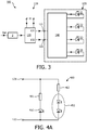
- FIG. 3 is a block diagram schematically illustrating the design of an illumination system 100 according to one embodiment of the present invention.
- this system has driver means 110 and an LED system 120 comprising four LEDs 21, 22, 23, 24.
- the driver means 110 comprises just one driver 130 having output terminals 131, 132, and the LED system 120 having input terminals 121, 122 comprises controllable current distribution means 140.
- the figure shows that the driver 130 is powered from the mains M, but it is noted that this, although typical, is not essential.
- a control device 2 may receive a user input signal Sui, and may control the driver 130. It is noted that this control device and driver may be integrated.
- the driver 130 has the characteristic of a current source.
- the driver 130 has the characteristic of a voltage source.
- the precise characteristic of the driver should not be interpreted as being a limiting factor. While an ideal voltage source has a vertical characteristic and an ideal current source has a horizontal characteristic, a realistic power source typically has a sloping characteristic intersecting both the current axis and the voltage axis. Nevertheless, in all cases, an LED driven by the driver may have the same working point (a point in the graph of figure 2 defined by the combination of actual voltage and actual current).
- the driver 130 has the characteristic of a voltage source, and that the control device 2 is capable of setting the driver output voltage. It is noted that LED drivers having a controllable output voltage are known per se, so that a detailed explanation thereof is not needed here. According to the principles proposed by the present invention, the output voltage of the driver 130, i.e. the input voltage received by the current distribution means 140, is considered to be a control parameter for the distribution of the current among the LEDs 21, 22, 23, 24.
- the current (function f i ) is only non-zero within a certain range of input voltages, while this range overlaps with a range of input voltages where all other LEDs have zero current, so that in this overlap range the light output has the pure color of said one LED or group of LEDs.
- the driver 130 supplies the summation of all LED currents.
- the current distribution means 140 does not comprise active processor means but consists of the hardware configuration of the LED system 120. In the following, some exemplary embodiments will be discussed.
- FIG 4A is a block diagram schematically illustrating an example of the LED system according to the present invention, indicated in general by the reference numeral 420.
- the input terminals are indicated by reference numerals 121, 122.
- the LED system 420 comprises two groups of LEDs 451, 452. These groups are connected in parallel to the input terminals 121, 122.
- An impedance 461 is connected in series with the first group 451 of LEDs.
- An impedance 462 is connected in series with the second group 452 of LEDs.In the following explanation, it will be assumed that this impedance is resistive, for instance a resistor.
- the first group 451 is shown by the symbol of a single LED, but this does not mean that there is only one LED in the first group.
- the group may actually comprise a plurality of LEDs arranged in series and/or in parallel with each other. These LEDs may be mutually identical, but the group may also comprise LEDs of mutually different colors. Apart from the LEDs, other electrical components may be connected in series and/or in parallel to the LEDs, for instance common diodes. While each individual LED or diode has its individual threshold voltage, as explained with reference to figure 2 , the group 451 as a whole has a group threshold voltage VT1 which typically corresponds to the summation of the threshold voltages of LEDs arranged in series. Thus, if the group 451 consists of a series arrangement of three identical LEDs each having an individual threshold voltage Vth, the group threshold voltage VT1 of the group is equal to 3Vth.
- the second group 452 has a group threshold voltage VT2, hereinafter simply indicated as second threshold voltage, larger than the group threshold voltage VT1 of the first group 451, hereinafter simply indicated as first threshold voltage.
- the impedance value of the second impedance 462 in series with the second LED group 452 may differ from the impedance value of the first impedance 461 in series with the first LED group 451.
- the impedance value of the second impedance 462 may be smaller than the impedance value of the first impedance 461, and the second impedance 462 may even be omitted, in which case the function of second impendance will be performed by the series wiring of the second LED group 452.
- figure 4B is a graph showing the light output L1 of the first group of LEDs 451 and the light output L2 of the second group of LEDs 452 as a function of the input voltage Vi received at the input terminals 121, 122 of the LED system 420.
- the ratio between R1 and R2 determines the ratio between the proportionality of L1 and L2 versus Vi, respectively.
- R2 is smaller than R1, so that the current in the second group 452 rises faster as a function of Vi as compared to the current in the first group 451, and it will be advantageous if the number of LEDs in the second group 452 is larger than the number of LEDs in the first group 451, such that all in all the second light output L2 rises faster than the first light output L1, as illustrated.
- the color points of the LEDs do not play any role. All individual LEDs may even be mutally identical.
- the group color point of the light output of all LEDs of the second group combined differs from the group color point of the light output of all LEDs of the first group combined, hereinafter simply indicated as first color point.
- first color point When all LED groups are placed relatively closely together, a human observer will perceive the overall light output as a blend having one blend color point.
- this blend color point travels in a straight line from the first color point towards the second color point.
- increasing the input voltage causes a change from red light to warm white light, which corresponds to the dimming of an incandescent lamp.
- Figure 4C illustrates a second example 430, in which the second group of LEDs 452 is connected to a node of a voltage divider 430 formed by two resistors 431, 432 connected in series between the input terminals 121, 122.
- this node provides a voltage derived from the input voltage Vi.
- the second group threshold voltage VT2 is lower than the first group threshold voltage, the second group 452 can only start to conduct if the input voltage Vi is equal to or higher than (R432 + R431)/R432 times VT2.
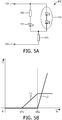
- Figure 5A illustrates a third example 470.
- Figure 5B is a graph comparable to figure 4B , illustrating the behaviour of this third embodiment 470.
- the second resistor 462 is replaced by a resistor 471 in series with the parallel arrangement of first group 451 and second group 452.
- the operation is the same as the operation of the first embodiment 420, with this difference that the current magnitude will be equal to (Vi - VT1)/(R1+R3), with R3 indicating the resistance of the common series resistor 471.
- the driver output voltage will result in the LED system 420; 470 as a whole generating a blend light output of which the color point travels in a straight line from the first color point towards the second color point.
- the first color point is substantially red and the second color point is substantially white.
- the first group 451 consists of precisely one red LED and the second group 452 consists of precisely two white LEDs arranged in series.
- the blend color point will not quite reach the second color point, because the first group 451 is on at all times when the second group 452 is on.
- the light colors may even be mutually equal.
- embodiments are possible where the individual LED groups are placed at a substantial distance from each other, so that for the human observer the light generated by the first group of LEDs originates from a different location than the light generated by the second group of LEDs. This can be used for generating special light effects, such as for instance running lights, a light tube, etc. Also in such embodiment, it would be desirable to be able to switch off the first group while the second group is on.
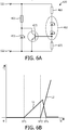
- Figure 6A illustrates a fourth example 620 of the LED system, comparable to the first embodiment 420 of figure 4A , where a current measuring sensor 672 is arranged between the cathode terminal of the second group 452 and the second input terminal 122, and where an NPN transistor 673 is arranged having its base terminal connected to the node between the current measuring sensor 672 and the second group of LEDs 452, having its emitter terminal connected to the second input terminal 122, and having its collector terminal connected to the node between the first resistor 461 and the first group of LEDs 451.
- NPN transistor instead of an NPN transistor, another type of controllable switch can be used, for instance a FET.
- the operation is as follows. For Vi smaller than VT2, the operation is the same as the operation of the first embodiment 420. When Vi is higher than VT2, current will also flow through the second group of LEDs 452, causing a voltage drop across the current measuring sensor 672. When this voltage drop becomes higher than the forward base-emitter bias of the transistor 673, the transistor starts to draw current causing the voltage drop across the first resistor 461 to increase and hence the voltage across the first group of LEDs 451 to decrease, so that L1 decreases with increasing input voltage Vi.
- Figure 6B is a graph comparable to figure 4B , showing that L1 eventually becomes equal to zero.
- the current through the first resistor 461 becomes equal to Vi/R1, which may be relatively high if R1 is relatively low.
- Vi/R1 the current through the first resistor 461 becomes equal to Vi/R1, which may be relatively high if R1 is relatively low.
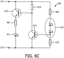
- the collector- emitter path of a second NPN transistor 674 is arranged between the first input terminal 121 and the first resistor 461.
- a bias resistor 675 is connected between the first input terminal 121 and the base terminal of said second NPN transistor 674.
- the collector terminal of the first NPN transistor 673 is connected to the node between the bias resistor 675 and the base terminal of said second NPN transistor 674.
- the operation is basically similar to the operation of LED system 620: when the input voltage rises above VT2, the increasing current in the second group of LEDs 452 will cause the base terminal of the second transistor 674 to be drawn to the level of the second input terminal 122, thus reducing and eventually cutting off the current in the first group of LEDs 451. Now the wasted current is limited by the bias resistor 675, which may have a much higher resistance than the first resistor 461.
- the light production response as a function of the input voltage Vi is mutually different for the individual groups of LEDs. This is caused by the groups having mutually different threshold voltages or receiving mutually different supply voltages derived from the input voltage, or both. Further, the ratio between the individual light outputs of the individual groups of LEDs is not constant. This even applies if the voltage-dependencies of the individual groups (dL/dVi) are mutually equal, which can be seen in figure 4B by giving the two sloping curves the same angle. In some of the embodiments, a coupling between one group and another group results in a decrease of one light output while the other light input increases as a function of the input voltage. All in all, in all embodiments, the overall color point of the combined light output is not constant but travels a path in color space as a function of input voltage Vi (unless of course the LEDs all emit the same color).
- the invention has been explained with two groups of LEDs 451, 452.
- the path traveled in color space is a straight line between the two color points corresponding to the two groups of LEDs.
- the inventive concept can be expanded in a modular fashion. So, it is possible to have a third group of LEDs, a fourth group of LEDs, etc, connected between the input terminals 121, 122, always with mutually different color point and mutually different threshold voltage.
- N groups of LEDs each group being indicated as G(i), with i being an index ranging from 1 to N, N being a positive integer larger than 1.
- Each group G(i) has a group threshold voltage VG(i) and a color point CP(i).
- CP(j) ⁇ CP(i) may apply, and preferably VG(j)>VG(i) applies.
- Each group G(i) is connected in series with at least one impedance.
- Two or more groups may be coupled such as to have one group influence the other group's response.
- two or more groups may have a common series impedance.
- a current reduction circuit for one group may be controlled by the current in another group. It is even possible to have an increasing current in group G(j) that reduces all the current in all groups G(i) with i ⁇ j; figure 6D schematically illustrates the modular layout of such a device.
- LED groups of 3 mutually different color points which may suitably be R, G, B, or there are at least 4 LED groups of 4 mutually different color points, which may suitably be R, G, B, W.
- Figure 7A illustrates an embodiment of an LED system 720 for a situation where the driver 130 is capable of providing a positive and a negative voltage.
- the LED system 720 comprises two systems 620 of figure 6A , individually distinguished as 620A and 620B, connected antiparallel between the input terminals 121, 122.
- 620A and 620B connected antiparallel between the input terminals 121, 122.
- the voltage at the first input terminal 121 is positive with respect to the second input terminal 122
- only the first system 620A is operative, and its operation is identical to the operation of LED system 620 as illustrated in figure 6B .
- the voltage at the first input terminal 121 is negative with respect to the second input terminal 122
- only the second system 620B is operative, and its operation again is identical to the operation of LED system 620 as illustrated in figure 6B .
- Figure 7B illustrates the overal light output as a function of Vi.
- L1 indicates the light output of group 451A.
- L2 indicates the light output of group 452A.
- L3 indicates the light output of group 451B.
- L4 indicates the light output of group 452B. It can be seen that for VT1 ⁇ Vi ⁇ VT2, the light output is pure L1; for Vi > Vx, the light output is pure L2; for VT4 ⁇ Vi ⁇ VT3, the light output is pure L3; for Vi ⁇ Vy, the light output is pure L4;
- this LED system 720 is capable of selectively providing light having the color points R or G or B or W by a suitable selection of the driver output voltage.
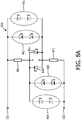
- Figure 8A illustrates an embodiment of an LED driver 820 that can be seen as a further elaboration of the embodiment 470 of figure 5A .
- the node between the first group of LEDs 451 and the first resistor 461 will be indicated as first node A, while the node between the first group of LEDs 451 and the common series resistor 471 will be indicated as second node B.
- the second group of LEDs 452 is connected between the first input terminal 121 and the second node B
- this embodiment 820 comprises a third group of LEDs 453 connected between the first node A and the second input terminal 122.
- this embodiment comprises a fourth group of LEDs 454 connected antiparallel with respect to the first group 451 between the first and the second node A and B, respectively.
- the third group 453 may have a third threshold voltage VT3 equal to or larger than the second threshold voltage VT2.
- the fourth group 454 has a fourth threshold voltage VT4.
- the third group has a third color point and the fourth group has a fourth color point.
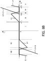
- Vi is smaller than VT1 and no current will flow.
- Vi In a second voltage range II, Vi is larger than VT1, and current only flows in the path formed by the series arrangement of resistor 461, first LEDs 451, and resistor 471.
- a voltage drop equal to VT1 will develop across the first LEDs 451.
- R461 R471.
- a fourth voltage range IV current only flows in a second and a third current path formed by the series arrangements of the second group 452 and resistor 471 and the series arrangements of the third group 453 and resistor 461, respectively.
- the voltage VA at the first node A will be equal to VT3, and the voltage VB at the second node B will be equal to Vi - VT2.
- the current in the second group 452 will be equal to (Vi - VT2)/R471
- the current in the third group 453 will be equal to (Vi - VT3)/R461.
- a third voltage range III between the second and fourth ranges, current flows in all of said paths, and first group 451, second group 452 and third group 453 are on.
- the precise current distribution between these paths will vary with Vi and will depend on the precise values of VT1, VT2, VT3, R461, R471.
- the lower boundary of the third voltage range III is determined by an input voltage level at which current flow becomes possible in the second or third path. As long as the voltage drop between first input terminal 121 and second node B, which can be expressed as V461 + VT1 or as Vi - V471, is smaller than VT2, no current will flow in the second path.
- the upper boundary of the third voltage range III is determined by an input voltage level at which current flow becomes impossible in the first path.
- the voltage difference between the two nodes A and B can be expressed as VT2 + VT3 - Vi. If this voltage difference is less than VT1, the first group 451 cannot conduct current.
- the upper boundary of the third voltage range III is equal to VT3 + VT2 - VT1.
- node A While initially node A is positive with respect to node B, it follows from the above that node A is negative with respect to node B if Vi > VT2 + VT3. If the negative voltage difference between nodes B and A becomes larger than VT4, the fourth group of LEDs 454 can conduct current. This occurs in a fifth range V where Vi > VT1 + VT2 + VT3.
- the four color points may be mutually different.
- the third group 453 has the same threshold voltage as the second group 452 and also has the same color point, while also the two resistors 461 and 471 have the same resistance value.
- the second and third groups are driven in a synchronous manner and produce the same light output color.
- the first group 451 has a red color point
- the second and third groups 452 and 453 have a white color point
- the fourth group 454 has a blue color point.
- Such an embodiment is particularly useful as a daylight lamp.
- the driver 130 is capable of providing a negative voltage, there will be a sixth operative range where current only flows in a fourth path defined by the series arrangement of second resistor 471, fourth group of LEDs 454, and first resistor 461.
- the description can be the same as for the second range II, with the first and fourth groups 451 and 454 having switched places.
- the device is capable of rendering three pure colors by suitably setting the input voltage for the LED system.
- the LED system 820 can be made completely symmetrical by adding a fifth group of LEDs 455 (curve L5 in figure 8B ) antiparallel to the second group of LEDs 452 and a sixth group of LEDs 456 (curve L6 in figure 8B ) antiparallel to the third group of LEDs, as illustrated in figure 8A in dotted lines.
- the color points of these fifth and sixth groups may be mutually equal. Further, the color points of these fifth and sixth groups may be equal to the color points of the second and third groups, but they may also be different to define a fourth color: in that case, there will be a seventh operative range where the output light only contains this fourth color, and the device is capable of rendering four pure colors by suitably setting the input voltage for the LED system.
- Figure 9 is a graph schematically illustrating the output voltage of the driver 130 (hence input voltage Vi) as a function of time.
- the control device 2 controls the driver 130 so that the output voltage Vi is within the second operative range II from time t1 to time t2, so the generated light output will have the first color point. From time t2 to time t3, the control device 2 controls the driver 130 so that the output voltage Vi is within the fourth operative range IV, so the generated light output will have the second/third color point.
- the control device 2 controls the driver 130 so that the output voltage Vi is within the sixth operative range VI, so the generated light output will have the color point of the fourth LEDs 454.
- the control device 2 controls the driver 130 so that the output voltage Vi is within the seventh operative range VII, so the generated light output will have the fourth color point of the fifth/sixth LEDs 455, 456.
- the time interval from t1 to t5 will be indicated as color period T.
- this color period T When this color period T is short enough, the human eye will not perceive a sequence of four different colors but rather a blend color; the precise color point of this blend color will depend on the precise durations of the four time intervals and on the precise voltage values within the four time intervals, as should be clear to a person skilled in the art.
- Figure 9A illustrates that the driver's output voltage Vi is maintained constant during said time intervals, but that is not necessary. It is even not necessary that the output voltage Vi is controlled stepwise: it is for instance possible that the output voltage Vi is controlled to have a wave shape such as a sawtooth or a sine.
- figure 9B shows a variation, wherein in each of the time intervals the voltage has the value discussed above for a first amount of time, and is zero for the remaining amount of time.
- the duty cycle of the voltage in this time interval By varying the duty cycle of the voltage in this time interval, the average intensity of the corresponding light output can be controlled between zero and a maximum.
- the present invention succeeds in providing an illumination system comprising an LED system and a single driver for driving this LED system, with a two-wire connection between driver and LED system, which illumination system is capable of rendering all colors within the color triangle RGB, or any other color triangle.
- the driver's output current can be used as a control parameter leading to a certain predetermined current distribution and hence output color.
Landscapes
- Circuit Arrangement For Electric Light Sources In General (AREA)
- Led Devices (AREA)
- Led Device Packages (AREA)
- Control Of Indicators Other Than Cathode Ray Tubes (AREA)
- Control Of El Displays (AREA)
Priority Applications (3)
| Application Number | Priority Date | Filing Date | Title |
|---|---|---|---|
| EP19154669.6A EP3512304A1 (en) | 2010-11-25 | 2011-11-15 | Illumination system comprising a plurality of leds |
| EP18153789.5A EP3349544A1 (en) | 2010-11-25 | 2011-11-15 | Illumination system comprising a plurality of leds |
| EP11799321.2A EP2644006B1 (en) | 2010-11-25 | 2011-11-15 | Illumination system comprising a plurality of leds |
Applications Claiming Priority (3)
| Application Number | Priority Date | Filing Date | Title |
|---|---|---|---|
| EP10192617 | 2010-11-25 | ||
| EP11799321.2A EP2644006B1 (en) | 2010-11-25 | 2011-11-15 | Illumination system comprising a plurality of leds |
| PCT/IB2011/055099 WO2012069961A1 (en) | 2010-11-25 | 2011-11-15 | Illumination system comprising a plurality of leds |
Related Child Applications (3)
| Application Number | Title | Priority Date | Filing Date |
|---|---|---|---|
| EP19154669.6A Division EP3512304A1 (en) | 2010-11-25 | 2011-11-15 | Illumination system comprising a plurality of leds |
| EP18153789.5A Division EP3349544A1 (en) | 2010-11-25 | 2011-11-15 | Illumination system comprising a plurality of leds |
| EP18153789.5A Division-Into EP3349544A1 (en) | 2010-11-25 | 2011-11-15 | Illumination system comprising a plurality of leds |
Publications (2)
| Publication Number | Publication Date |
|---|---|
| EP2644006A1 EP2644006A1 (en) | 2013-10-02 |
| EP2644006B1 true EP2644006B1 (en) | 2018-03-28 |
Family
ID=45375462
Family Applications (3)
| Application Number | Title | Priority Date | Filing Date |
|---|---|---|---|
| EP18153789.5A Withdrawn EP3349544A1 (en) | 2010-11-25 | 2011-11-15 | Illumination system comprising a plurality of leds |
| EP19154669.6A Pending EP3512304A1 (en) | 2010-11-25 | 2011-11-15 | Illumination system comprising a plurality of leds |
| EP11799321.2A Active EP2644006B1 (en) | 2010-11-25 | 2011-11-15 | Illumination system comprising a plurality of leds |
Family Applications Before (2)
| Application Number | Title | Priority Date | Filing Date |
|---|---|---|---|
| EP18153789.5A Withdrawn EP3349544A1 (en) | 2010-11-25 | 2011-11-15 | Illumination system comprising a plurality of leds |
| EP19154669.6A Pending EP3512304A1 (en) | 2010-11-25 | 2011-11-15 | Illumination system comprising a plurality of leds |
Country Status (9)
| Country | Link |
|---|---|
| US (1) | US9119260B2 (ja) |
| EP (3) | EP3349544A1 (ja) |
| JP (1) | JP5977250B2 (ja) |
| CN (1) | CN103222339B (ja) |
| BR (1) | BR112013012675B1 (ja) |
| ES (1) | ES2671599T3 (ja) |
| RU (1) | RU2572587C2 (ja) |
| TW (1) | TW201233247A (ja) |
| WO (1) | WO2012069961A1 (ja) |
Families Citing this family (9)
| Publication number | Priority date | Publication date | Assignee | Title |
|---|---|---|---|---|
| JP2014078374A (ja) * | 2012-10-10 | 2014-05-01 | Rohm Co Ltd | 照明機器 |
| DE102013207245B4 (de) * | 2013-04-22 | 2015-12-03 | Osram Gmbh | Ansteuerung von Halbleiterleuchtelementen sowie Lampe, Leuchte oder Leuchtsystem mit einer solchen Ansteuerung |
| JP5760044B2 (ja) * | 2013-06-14 | 2015-08-05 | フェニックス電機株式会社 | Ledランプ |
| DE102014206434A1 (de) * | 2014-04-03 | 2015-10-08 | Osram Gmbh | Ansteuerung von Halbleiterleuchtelementen |
| EP3193564B1 (en) * | 2014-09-08 | 2021-04-07 | Citizen Watch Co., Ltd. | Led drive circuit |
| JP6536967B2 (ja) * | 2017-04-12 | 2019-07-03 | Zigenライティングソリューション株式会社 | 発光装置および照明装置 |
| KR102166270B1 (ko) * | 2018-08-08 | 2020-10-15 | 한국광기술원 | 분기 회로 및 그를 포함한 미세 led 패키지 |
| JP6886450B2 (ja) * | 2018-11-30 | 2021-06-16 | コイト電工株式会社 | 電源調整システム |
| JP7147656B2 (ja) * | 2019-03-27 | 2022-10-05 | 株式会社デンソーエレクトロニクス | 負荷駆動装置 |
Family Cites Families (19)
| Publication number | Priority date | Publication date | Assignee | Title |
|---|---|---|---|---|
| JP4495814B2 (ja) * | 1999-12-28 | 2010-07-07 | アビックス株式会社 | 調光式led照明器具 |
| GB0015559D0 (en) | 2000-06-27 | 2000-08-16 | Oxley Dev Co Ltd | Device controller and control arrangement |
| JP2002016290A (ja) * | 2000-06-28 | 2002-01-18 | Toshiba Lighting & Technology Corp | Led光源装置 |
| US6323598B1 (en) * | 2000-09-29 | 2001-11-27 | Aerospace Optics, Inc. | Enhanced trim resolution voltage-controlled dimming led driver |
| US6653798B2 (en) * | 2000-09-29 | 2003-11-25 | Aerospace Optics, Inc. | Voltage dimmable LED display producing multiple colors |
| JP3082719U (ja) * | 2001-06-15 | 2001-12-26 | 舶用電球株式会社 | Ledランプ |
| DE10214195B4 (de) | 2002-03-28 | 2004-08-05 | Siteco Beleuchtungstechnik Gmbh | Leuchtensystem und Verfahren zum Ansteuern von mindestens zwei Leuchtmitteln |
| JP4959324B2 (ja) * | 2003-05-07 | 2012-06-20 | コーニンクレッカ フィリップス エレクトロニクス エヌ ヴィ | 複数の発光ダイオードのための単一ドライバ |
| JP2006253215A (ja) * | 2005-03-08 | 2006-09-21 | Sharp Corp | 発光装置 |
| DE102005014612A1 (de) * | 2005-03-31 | 2006-10-05 | Bally Wulff Holding Gmbh & Co. Kg | Schaltungsanordnung zur Helligkeitsregelung bei mehrfarbigen Leuchtdioden |
| ATE515177T1 (de) * | 2006-05-02 | 2011-07-15 | Koninkl Philips Electronics Nv | Leuchtdiodenschaltung, anordnung und vorrichtung |
| JP5198442B2 (ja) | 2006-06-23 | 2013-05-15 | コーニンクレッカ フィリップス エレクトロニクス エヌ ヴィ | 光源のアレイを駆動する方法及びデバイス |
| US7703943B2 (en) * | 2007-05-07 | 2010-04-27 | Intematix Corporation | Color tunable light source |
| JP2009158507A (ja) * | 2007-12-25 | 2009-07-16 | Panasonic Electric Works Co Ltd | Led発光装置およびそれを用いた照明器具 |
| TW200934294A (en) * | 2008-01-24 | 2009-08-01 | Everbright Optech Inc | Apparatus for controlling light emitting devices |
| US8004216B2 (en) * | 2008-05-02 | 2011-08-23 | The United States Of America As Represented By The Secretary Of The Navy | Variable intensity LED illumination system |
| JP2010050010A (ja) * | 2008-07-24 | 2010-03-04 | Nippon Seiki Co Ltd | 照明装置 |
| EP2366269B1 (en) | 2008-11-13 | 2012-10-10 | Koninklijke Philips Electronics N.V. | Lighting system with a plurality of leds |
| JP5807195B2 (ja) * | 2010-04-08 | 2015-11-10 | パナソニックIpマネジメント株式会社 | 発光装置 |
-
2011
- 2011-11-15 JP JP2013540462A patent/JP5977250B2/ja active Active
- 2011-11-15 BR BR112013012675-2A patent/BR112013012675B1/pt active IP Right Grant
- 2011-11-15 ES ES11799321.2T patent/ES2671599T3/es active Active
- 2011-11-15 CN CN201180056689.4A patent/CN103222339B/zh active Active
- 2011-11-15 WO PCT/IB2011/055099 patent/WO2012069961A1/en active Application Filing
- 2011-11-15 US US13/988,140 patent/US9119260B2/en active Active
- 2011-11-15 EP EP18153789.5A patent/EP3349544A1/en not_active Withdrawn
- 2011-11-15 RU RU2013128872/07A patent/RU2572587C2/ru active
- 2011-11-15 EP EP19154669.6A patent/EP3512304A1/en active Pending
- 2011-11-15 EP EP11799321.2A patent/EP2644006B1/en active Active
- 2011-11-24 TW TW100143220A patent/TW201233247A/zh unknown
Also Published As
| Publication number | Publication date |
|---|---|
| EP2644006A1 (en) | 2013-10-02 |
| EP3349544A1 (en) | 2018-07-18 |
| WO2012069961A1 (en) | 2012-05-31 |
| JP2014502411A (ja) | 2014-01-30 |
| TW201233247A (en) | 2012-08-01 |
| BR112013012675A8 (pt) | 2017-07-11 |
| US20130234619A1 (en) | 2013-09-12 |
| CN103222339B (zh) | 2016-03-16 |
| US9119260B2 (en) | 2015-08-25 |
| BR112013012675B1 (pt) | 2020-12-01 |
| RU2013128872A (ru) | 2014-12-27 |
| CN103222339A (zh) | 2013-07-24 |
| ES2671599T3 (es) | 2018-06-07 |
| BR112013012675A2 (pt) | 2016-09-13 |
| JP5977250B2 (ja) | 2016-08-24 |
| RU2572587C2 (ru) | 2016-01-20 |
| EP3512304A1 (en) | 2019-07-17 |
Similar Documents
| Publication | Publication Date | Title |
|---|---|---|
| EP2644006B1 (en) | Illumination system comprising a plurality of leds | |
| US7884556B2 (en) | Color-changing light array device | |
| US7489089B2 (en) | Color control system for color changing lights | |
| KR101493492B1 (ko) | 백라이트 유닛, 이를 포함하는 액정 표시 장치 및 이의구동방법 | |
| KR101494320B1 (ko) | 백라이트 어셈블리 및 이를 갖는 표시장치 | |
| EP2078446B1 (en) | A switched light element array and method of operation | |
| US20060108933A1 (en) | Light emitted diode driving apparatus | |
| EP2645815A1 (en) | LED lighting system | |
| WO2016070150A1 (en) | System for adaptive non-linear light dimming of electro-optical devices | |
| JP2005197304A (ja) | 発光装置 | |
| JP5858253B2 (ja) | 発光デバイスおよびその電流制御モジュール | |
| JP2013047735A (ja) | 表示装置 | |
| KR20140120168A (ko) | 유기 전계 발광 표시 장치 및 이의 구동 방법 | |
| CN212544114U (zh) | 具高精度控制的电流控制装置 | |
| CN114830827A (zh) | 发光二极管阵列的动态亮度的控制 | |
| JP2019075386A (ja) | 発光装置の制御回路および発光装置 | |
| CN206516326U (zh) | 显示电路和电子设备 | |
| JP2008004731A (ja) | 発光ダイオード定電流パルス幅制御駆動回路 | |
| US20230225024A1 (en) | Illuminating leds | |
| JP2006135227A (ja) | 発光ダイオードの点灯回路および制御方法 | |
| TW201419931A (zh) | 發光二極體控制電路 | |
| JP2007147668A (ja) | 交流用led点灯回路 | |
| US20140132161A1 (en) | Method for Using Constant Current Driving Chip to Generate Different Currents to Drive Light Bar and Driving Circuit Thereof | |
| TWM376097U (en) | Lightness adjustment circuit | |
| JPH0710789U (ja) | 発光素子輝度調整装置 |
Legal Events
| Date | Code | Title | Description |
|---|---|---|---|
| PUAI | Public reference made under article 153(3) epc to a published international application that has entered the european phase |
Free format text: ORIGINAL CODE: 0009012 |
|
| 17P | Request for examination filed |
Effective date: 20130625 |
|
| AK | Designated contracting states |
Kind code of ref document: A1 Designated state(s): AL AT BE BG CH CY CZ DE DK EE ES FI FR GB GR HR HU IE IS IT LI LT LU LV MC MK MT NL NO PL PT RO RS SE SI SK SM TR |
|
| DAX | Request for extension of the european patent (deleted) | ||
| 17Q | First examination report despatched |
Effective date: 20140826 |
|
| RAP1 | Party data changed (applicant data changed or rights of an application transferred) |
Owner name: PHILIPS LIGHTING HOLDING B.V. |
|
| GRAP | Despatch of communication of intention to grant a patent |
Free format text: ORIGINAL CODE: EPIDOSNIGR1 |
|
| INTG | Intention to grant announced |
Effective date: 20171011 |
|
| GRAS | Grant fee paid |
Free format text: ORIGINAL CODE: EPIDOSNIGR3 |
|
| GRAA | (expected) grant |
Free format text: ORIGINAL CODE: 0009210 |
|
| AK | Designated contracting states |
Kind code of ref document: B1 Designated state(s): AL AT BE BG CH CY CZ DE DK EE ES FI FR GB GR HR HU IE IS IT LI LT LU LV MC MK MT NL NO PL PT RO RS SE SI SK SM TR |
|
| REG | Reference to a national code |
Ref country code: GB Ref legal event code: FG4D |
|
| REG | Reference to a national code |
Ref country code: CH Ref legal event code: EP |
|
| REG | Reference to a national code |
Ref country code: AT Ref legal event code: REF Ref document number: 984528 Country of ref document: AT Kind code of ref document: T Effective date: 20180415 |
|
| REG | Reference to a national code |
Ref country code: IE Ref legal event code: FG4D |
|
| REG | Reference to a national code |
Ref country code: DE Ref legal event code: R096 Ref document number: 602011046964 Country of ref document: DE |
|
| REG | Reference to a national code |
Ref country code: ES Ref legal event code: FG2A Ref document number: 2671599 Country of ref document: ES Kind code of ref document: T3 Effective date: 20180607 |
|
| PG25 | Lapsed in a contracting state [announced via postgrant information from national office to epo] |
Ref country code: FI Free format text: LAPSE BECAUSE OF FAILURE TO SUBMIT A TRANSLATION OF THE DESCRIPTION OR TO PAY THE FEE WITHIN THE PRESCRIBED TIME-LIMIT Effective date: 20180328 Ref country code: NO Free format text: LAPSE BECAUSE OF FAILURE TO SUBMIT A TRANSLATION OF THE DESCRIPTION OR TO PAY THE FEE WITHIN THE PRESCRIBED TIME-LIMIT Effective date: 20180628 Ref country code: HR Free format text: LAPSE BECAUSE OF FAILURE TO SUBMIT A TRANSLATION OF THE DESCRIPTION OR TO PAY THE FEE WITHIN THE PRESCRIBED TIME-LIMIT Effective date: 20180328 Ref country code: LT Free format text: LAPSE BECAUSE OF FAILURE TO SUBMIT A TRANSLATION OF THE DESCRIPTION OR TO PAY THE FEE WITHIN THE PRESCRIBED TIME-LIMIT Effective date: 20180328 |
|
| REG | Reference to a national code |
Ref country code: NL Ref legal event code: MP Effective date: 20180328 |
|
| REG | Reference to a national code |
Ref country code: LT Ref legal event code: MG4D |
|
| PG25 | Lapsed in a contracting state [announced via postgrant information from national office to epo] |
Ref country code: GR Free format text: LAPSE BECAUSE OF FAILURE TO SUBMIT A TRANSLATION OF THE DESCRIPTION OR TO PAY THE FEE WITHIN THE PRESCRIBED TIME-LIMIT Effective date: 20180629 Ref country code: LV Free format text: LAPSE BECAUSE OF FAILURE TO SUBMIT A TRANSLATION OF THE DESCRIPTION OR TO PAY THE FEE WITHIN THE PRESCRIBED TIME-LIMIT Effective date: 20180328 Ref country code: SE Free format text: LAPSE BECAUSE OF FAILURE TO SUBMIT A TRANSLATION OF THE DESCRIPTION OR TO PAY THE FEE WITHIN THE PRESCRIBED TIME-LIMIT Effective date: 20180328 Ref country code: BG Free format text: LAPSE BECAUSE OF FAILURE TO SUBMIT A TRANSLATION OF THE DESCRIPTION OR TO PAY THE FEE WITHIN THE PRESCRIBED TIME-LIMIT Effective date: 20180628 Ref country code: RS Free format text: LAPSE BECAUSE OF FAILURE TO SUBMIT A TRANSLATION OF THE DESCRIPTION OR TO PAY THE FEE WITHIN THE PRESCRIBED TIME-LIMIT Effective date: 20180328 |
|
| PG25 | Lapsed in a contracting state [announced via postgrant information from national office to epo] |
Ref country code: NL Free format text: LAPSE BECAUSE OF FAILURE TO SUBMIT A TRANSLATION OF THE DESCRIPTION OR TO PAY THE FEE WITHIN THE PRESCRIBED TIME-LIMIT Effective date: 20180328 Ref country code: PL Free format text: LAPSE BECAUSE OF FAILURE TO SUBMIT A TRANSLATION OF THE DESCRIPTION OR TO PAY THE FEE WITHIN THE PRESCRIBED TIME-LIMIT Effective date: 20180328 Ref country code: EE Free format text: LAPSE BECAUSE OF FAILURE TO SUBMIT A TRANSLATION OF THE DESCRIPTION OR TO PAY THE FEE WITHIN THE PRESCRIBED TIME-LIMIT Effective date: 20180328 Ref country code: AL Free format text: LAPSE BECAUSE OF FAILURE TO SUBMIT A TRANSLATION OF THE DESCRIPTION OR TO PAY THE FEE WITHIN THE PRESCRIBED TIME-LIMIT Effective date: 20180328 Ref country code: RO Free format text: LAPSE BECAUSE OF FAILURE TO SUBMIT A TRANSLATION OF THE DESCRIPTION OR TO PAY THE FEE WITHIN THE PRESCRIBED TIME-LIMIT Effective date: 20180328 |
|
| PG25 | Lapsed in a contracting state [announced via postgrant information from national office to epo] |
Ref country code: CZ Free format text: LAPSE BECAUSE OF FAILURE TO SUBMIT A TRANSLATION OF THE DESCRIPTION OR TO PAY THE FEE WITHIN THE PRESCRIBED TIME-LIMIT Effective date: 20180328 Ref country code: SM Free format text: LAPSE BECAUSE OF FAILURE TO SUBMIT A TRANSLATION OF THE DESCRIPTION OR TO PAY THE FEE WITHIN THE PRESCRIBED TIME-LIMIT Effective date: 20180328 Ref country code: SK Free format text: LAPSE BECAUSE OF FAILURE TO SUBMIT A TRANSLATION OF THE DESCRIPTION OR TO PAY THE FEE WITHIN THE PRESCRIBED TIME-LIMIT Effective date: 20180328 |
|
| RAP2 | Party data changed (patent owner data changed or rights of a patent transferred) |
Owner name: PHILIPS LIGHTING HOLDING B.V. |
|
| REG | Reference to a national code |
Ref country code: AT Ref legal event code: MK05 Ref document number: 984528 Country of ref document: AT Kind code of ref document: T Effective date: 20180328 |
|
| PG25 | Lapsed in a contracting state [announced via postgrant information from national office to epo] |
Ref country code: PT Free format text: LAPSE BECAUSE OF FAILURE TO SUBMIT A TRANSLATION OF THE DESCRIPTION OR TO PAY THE FEE WITHIN THE PRESCRIBED TIME-LIMIT Effective date: 20180730 |
|
| REG | Reference to a national code |
Ref country code: DE Ref legal event code: R097 Ref document number: 602011046964 Country of ref document: DE |
|
| PG25 | Lapsed in a contracting state [announced via postgrant information from national office to epo] |
Ref country code: DK Free format text: LAPSE BECAUSE OF FAILURE TO SUBMIT A TRANSLATION OF THE DESCRIPTION OR TO PAY THE FEE WITHIN THE PRESCRIBED TIME-LIMIT Effective date: 20180328 Ref country code: AT Free format text: LAPSE BECAUSE OF FAILURE TO SUBMIT A TRANSLATION OF THE DESCRIPTION OR TO PAY THE FEE WITHIN THE PRESCRIBED TIME-LIMIT Effective date: 20180328 |
|
| PLBE | No opposition filed within time limit |
Free format text: ORIGINAL CODE: 0009261 |
|
| STAA | Information on the status of an ep patent application or granted ep patent |
Free format text: STATUS: NO OPPOSITION FILED WITHIN TIME LIMIT |
|
| 26N | No opposition filed |
Effective date: 20190103 |
|
| PG25 | Lapsed in a contracting state [announced via postgrant information from national office to epo] |
Ref country code: SI Free format text: LAPSE BECAUSE OF FAILURE TO SUBMIT A TRANSLATION OF THE DESCRIPTION OR TO PAY THE FEE WITHIN THE PRESCRIBED TIME-LIMIT Effective date: 20180328 |
|
| REG | Reference to a national code |
Ref country code: CH Ref legal event code: PL |
|
| PG25 | Lapsed in a contracting state [announced via postgrant information from national office to epo] |
Ref country code: LU Free format text: LAPSE BECAUSE OF NON-PAYMENT OF DUE FEES Effective date: 20181115 Ref country code: MC Free format text: LAPSE BECAUSE OF FAILURE TO SUBMIT A TRANSLATION OF THE DESCRIPTION OR TO PAY THE FEE WITHIN THE PRESCRIBED TIME-LIMIT Effective date: 20180328 |
|
| REG | Reference to a national code |
Ref country code: BE Ref legal event code: MM Effective date: 20181130 |
|
| REG | Reference to a national code |
Ref country code: IE Ref legal event code: MM4A |
|
| PG25 | Lapsed in a contracting state [announced via postgrant information from national office to epo] |
Ref country code: LI Free format text: LAPSE BECAUSE OF NON-PAYMENT OF DUE FEES Effective date: 20181130 Ref country code: CH Free format text: LAPSE BECAUSE OF NON-PAYMENT OF DUE FEES Effective date: 20181130 |
|
| PG25 | Lapsed in a contracting state [announced via postgrant information from national office to epo] |
Ref country code: IE Free format text: LAPSE BECAUSE OF NON-PAYMENT OF DUE FEES Effective date: 20181115 |
|
| REG | Reference to a national code |
Ref country code: DE Ref legal event code: R079 Ref document number: 602011046964 Country of ref document: DE Free format text: PREVIOUS MAIN CLASS: H05B0033080000 Ipc: H05B0045000000 |
|
| PG25 | Lapsed in a contracting state [announced via postgrant information from national office to epo] |
Ref country code: BE Free format text: LAPSE BECAUSE OF NON-PAYMENT OF DUE FEES Effective date: 20181130 |
|
| PG25 | Lapsed in a contracting state [announced via postgrant information from national office to epo] |
Ref country code: MT Free format text: LAPSE BECAUSE OF NON-PAYMENT OF DUE FEES Effective date: 20181115 |
|
| PG25 | Lapsed in a contracting state [announced via postgrant information from national office to epo] |
Ref country code: TR Free format text: LAPSE BECAUSE OF FAILURE TO SUBMIT A TRANSLATION OF THE DESCRIPTION OR TO PAY THE FEE WITHIN THE PRESCRIBED TIME-LIMIT Effective date: 20180328 |
|
| PG25 | Lapsed in a contracting state [announced via postgrant information from national office to epo] |
Ref country code: CY Free format text: LAPSE BECAUSE OF FAILURE TO SUBMIT A TRANSLATION OF THE DESCRIPTION OR TO PAY THE FEE WITHIN THE PRESCRIBED TIME-LIMIT Effective date: 20180328 Ref country code: HU Free format text: LAPSE BECAUSE OF FAILURE TO SUBMIT A TRANSLATION OF THE DESCRIPTION OR TO PAY THE FEE WITHIN THE PRESCRIBED TIME-LIMIT; INVALID AB INITIO Effective date: 20111115 Ref country code: MK Free format text: LAPSE BECAUSE OF NON-PAYMENT OF DUE FEES Effective date: 20180328 |
|
| PG25 | Lapsed in a contracting state [announced via postgrant information from national office to epo] |
Ref country code: IS Free format text: LAPSE BECAUSE OF FAILURE TO SUBMIT A TRANSLATION OF THE DESCRIPTION OR TO PAY THE FEE WITHIN THE PRESCRIBED TIME-LIMIT Effective date: 20180728 |
|
| REG | Reference to a national code |
Ref country code: ES Ref legal event code: PC2A Owner name: SIGNIFY HOLDING B.V. Effective date: 20201015 |
|
| REG | Reference to a national code |
Ref country code: DE Ref legal event code: R081 Ref document number: 602011046964 Country of ref document: DE Owner name: SIGNIFY HOLDING B.V., NL Free format text: FORMER OWNER: PHILIPS LIGHTING HOLDING B.V., EINDHOVEN, NL |
|
| P01 | Opt-out of the competence of the unified patent court (upc) registered |
Effective date: 20230421 |
|
| PGFP | Annual fee paid to national office [announced via postgrant information from national office to epo] |
Ref country code: GB Payment date: 20231121 Year of fee payment: 13 |
|
| PGFP | Annual fee paid to national office [announced via postgrant information from national office to epo] |
Ref country code: ES Payment date: 20231219 Year of fee payment: 13 |
|
| PGFP | Annual fee paid to national office [announced via postgrant information from national office to epo] |
Ref country code: IT Payment date: 20231124 Year of fee payment: 13 Ref country code: FR Payment date: 20231123 Year of fee payment: 13 |
|
| PGFP | Annual fee paid to national office [announced via postgrant information from national office to epo] |
Ref country code: DE Payment date: 20240129 Year of fee payment: 13 |