EP2626787B1 - Data comparison apparatus, data comparison method and safety system using the same - Google Patents
Data comparison apparatus, data comparison method and safety system using the same Download PDFInfo
- Publication number
- EP2626787B1 EP2626787B1 EP13154229.2A EP13154229A EP2626787B1 EP 2626787 B1 EP2626787 B1 EP 2626787B1 EP 13154229 A EP13154229 A EP 13154229A EP 2626787 B1 EP2626787 B1 EP 2626787B1
- Authority
- EP
- European Patent Office
- Prior art keywords
- data
- synchronization
- comparison
- cpus
- circuit
- Prior art date
- Legal status (The legal status is an assumption and is not a legal conclusion. Google has not performed a legal analysis and makes no representation as to the accuracy of the status listed.)
- Not-in-force
Links
Images


Classifications
-
- G—PHYSICS
- G06—COMPUTING OR CALCULATING; COUNTING
- G06F—ELECTRIC DIGITAL DATA PROCESSING
- G06F11/00—Error detection; Error correction; Monitoring
- G06F11/07—Responding to the occurrence of a fault, e.g. fault tolerance
- G06F11/16—Error detection or correction of the data by redundancy in hardware
- G06F11/1675—Temporal synchronisation or re-synchronisation of redundant processing components
- G06F11/1679—Temporal synchronisation or re-synchronisation of redundant processing components at clock signal level
-
- G—PHYSICS
- G06—COMPUTING OR CALCULATING; COUNTING
- G06F—ELECTRIC DIGITAL DATA PROCESSING
- G06F11/00—Error detection; Error correction; Monitoring
- G06F11/07—Responding to the occurrence of a fault, e.g. fault tolerance
- G06F11/16—Error detection or correction of the data by redundancy in hardware
- G06F11/1629—Error detection by comparing the output of redundant processing systems
- G06F11/1641—Error detection by comparing the output of redundant processing systems where the comparison is not performed by the redundant processing components
Definitions
- the present invention relates to data comparison apparatus, a data comparison method and a safety system using the same.
- a data comparison apparatus, a data comparison method and a safety system that can be used in a railway signaling system, such as a train control system (an automatic train protection system (ATP) or an automatic train control system (ATC)) and an interlocking system.
- ATP automatic train protection system
- ATC automatic train control system
- Patent Document 1 discloses a related art. In this publication, a description is found that "a clock synchronization type 2-out-of-2 system is a system that ensures high reliability and safety in a computer-based control system".
- Patent Document 1 a mechanism used in a computer-based control system with high safety is described that has two CPUs and a failsafe comparison circuit that detects a fault of the CPUs by checking whether the data output from the CPUs are matched or unmatched.
- the clock synchronization type 2-out-of-2 system described in Patent Document 1 cannot precisely compare the data sent from the two CPUs when the data are out of synchronization.
- the circuit can hardly precisely detect a fault of the CPUs if the data output from the two CPUs are not in perfect synchronization with each other, such as when the two CPUs operate on independent clocks or when the two CPUs are of different types.
- An object of the present invention is to provide a data comparison apparatus that can detect a synchronization loss between data sent from at least two CPUs and adjust the comparison timing to compare the data, a data comparison method therefor and a safety system using the same.
- US 2011/0254602 proposes a method and circuit for synchronizing a first circuit and a second circuit.
- a first aspect of the present invention provides a data comparison apparatus according to claim 1.
- a second aspect of the present invention provides a safety system according to claim 6.
- a third aspect of the present invention provides a data comparison method according to claim 12.
- the present invention provides a data comparison apparatus that can detect a synchronization loss between data sent from a plurality of data sources and adjust the comparison timing to compare the data, a data comparison method therefor and a safety system using the same.
- a comparative example 1 described below concerns an example of a data comparison apparatus that can detect a synchronization loss between data sent from a plurality of data sources and adjust the comparison timing to compare the data.
- FIG. 1 is a diagram showing an example of a configuration of the data comparison apparatus according to the comparative example 1.
- the data comparison apparatus according to this comparative example comprises a synchronization signal generating circuit 10, a synchronization loss detecting circuit 20 and a synchronization adjusting comparison circuit 30 and is designed to compare data sent from two data sources that can be out of synchronization.
- the synchronization signal generating circuit 10 comprises a synchronization trigger detecting part 11 and a synchronization signal generating part 12 for each data source.
- the synchronization trigger detecting part 11 detects any particular input bit string in data 1a or 1b input from the associated data source and informs the associated synchronization signal generating part 12 that the particular bit string is input from the data source.
- the particular bit string may be any bit string that complies with the transmission protocol of the data sent from the data source, such as a start bit used in the short-stop synchronization system and a preamble used in Ethernet (registered trademark).
- a clock signal having a sufficiently short period is needed to detect a trigger.
- the clock signal may be externally input or generated by an.internal clock.
- the synchronization signal generating part 12 If the synchronization signal generating part 12 is informed by the synchronization trigger detecting part 11 that the particular bit string is input from the data source, the synchronization signal generating part 12 generates a synchronization signal 3 and transmits the synchronization signal 3 to the synchronization loss detecting circuit 20.
- the synchronization signal 3 may be any signal that can be used for observation of a synchronization loss, such as an M-sequence signal.
- the synchronization signal generating circuit 10 generates a clock signal 4 having a sufficiently short period for comparison of the synchronization signals 3 or adjustment of the comparison timing and provides the clock signal 4 to the synchronization loss detecting circuit 20 and the synchronization adjusting comparison circuit 30.
- the synchronization loss detecting circuit 20 comprises a synchronization signal shift register 21 for each data source, and a synchronization loss detecting part 22 that compares the synchronization signals 3 from the synchronization signal shift registers 21.
- the synchronization signal shift register 21 stores the synchronization signal 3 for the associated data source input from the synchronization signal generating circuit 10.
- the synchronization loss detecting part 22 detects a synchronization loss between the data 1a and 1b sent from the data sources by comparing the synchronization signals 3 stored in the synchronization signal shift registers 21 in terms of specific characteristics thereof. For example, in the case where the synchronization signals 3 are M-sequence signals "1001110" having a period of 7, a synchronization loss between the signals can be detected by comparing three bits at the same time. When the three bits of one synchronization signal are 100, it can be detected that a 1-bit phase error has occurred if the three bits of the other are 001, a 2-bit phase error has occurred if the three bits of the other are 011, and a 3-bit phase error has occurred if the three bits of the other are 111.
- the synchronization signal 3 having a period of 7 does not allow detection of a phase error of 7 or more bits. Thus, it is preferred that possible phase errors between the data 1a and 1b, the synchronization loss between which is to be detected, are examined in advance, and synchronization signals 3 having a sufficiently long period for those phase errors is used.
- the synchronization signal shift register 21 also preferably has a sufficiently large number of stages to detect the possible phase errors between the synchronization signals 3 used.
- the synchronization adjusting comparison circuit 30 is informed of the detected phase error as a synchronization adjustment signal 5.
- the synchronization adjustment signal 5 may be any signal that shows the number of bits of the phase error, such as a selection control signal for a multiplexer 32 that is shifted by the number of bits of the phase error.
- the synchronization adjusting comparison circuit 30 comprises a comparison shift register 31 and a multiplexer 32 for each data source and an exclusive-OR circuit 33 that compares the data 1a and 1b from the data sources.
- the comparison shift register 31 stores the data 1a or 1b input from the associated data source.
- a four-stage shift register cannot adjust a phase error of 4 or more bits.
- the multiplexer 32 selects from among the data stored in the comparison shift register 31 based on the synchronization adjustment signal 5 input from the synchronization loss detecting circuit 20 and outputs the selected data, and the exclusive-OR circuit 33 compares the data 1a and 1b and outputs a data comparison result 2.
- the data comparison apparatus can detect the synchronization loss between the data 1a and 1b and adjust the comparison timing to compare the data 1a and 1b.
- a comparative example 2 described below concerns an example of a safety system that has a plurality of CPUs and a data comparison apparatus that can detect a synchronization loss between data sent from the CPUs performing the same data processing and adjust the comparison timing to compare the data.
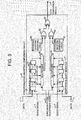
- FIG. 2 is a diagram showing a comparative example of a configuration of the safety system that comprises two CPUs and a data comparison apparatus.
- the safety system according to this comparative example comprises a CPU 40, a CPU 41 and a data comparison apparatus 42.
- the data comparison apparatus 42 has the same configuration as the data comparison apparatus according to the comparative example 1 described above and comprises the synchronization signal generating circuit 10, the synchronization loss detecting circuit 20 and the synchronization adjusting comparison circuit 30.
- the CPUs 40 and 41 first perform the same data processing for the safety system.
- Data 1c and 1d which are data processing results output from the CPUs 40 and 41, respectively, are input to the synchronization signal generating circuit 10 and the synchronization adjusting comparison circuit 30 of the data comparison apparatus 42. Then, the data comparison apparatus 42 compares the data 1c and 1d output from the CPUs 40 and 41 that can be out of synchronization through the same operation as in the comparative example 1.
- the safety system can ensure the system safety by stopping the CPU through an interruption processing, cutting off the power supply or shutting down the external interface.
- the safety system according to this embodiment can be configured to make the CPUs 40 and 41 operate on different clocks to ensure higher safety than in the case where the CPUs 40 and 41 operate on the same clock.
- the output data may not go out of synchronization if the processing speeds of both CPUs decrease in the same rate. Therefore, the fault cannot be detected by data comparison.
- the safety system according to this embodiment can be configured to have CPUs 40 and 41 of different types to ensure higher safety than in the case where the CPUs 40 and 41 are of the same type.
- the probability that the erroneous output data differs from the data output from the other CPU is extremely high.
- the data comparison shows that the data 1c and 1d do not match each other, so that the fault can be detected.
- the safety system can adjust the comparison timing to compare data that are output from a plurality of CPUs performing the same data processing and can be out of synchronization.
- the safety system can ensure higher safety.than conventional safety systems that are. configured so that two CPUs of the same type operate on one clock.
- An embodiment 1 described below concerns an example of a safety system that incorporates a data comparison apparatus that can not only detect a synchronization loss between data sent from a plurality of CPUs and adjust the comparison timing to compare the data but also prevent latency of a failure in the apparatus.
- the safety system according to this embodiment is an example of the safety system according to the comparative example 2 that further comprises an orthogonal waveform generating circuit 34, an orthogonal waveform generating circuit 35, an exclusive-OR circuit 36 and an exclusive-OR circuit 37 provided between the multiplexer 32 and the exclusive-OR circuit 33 in the synchronization adjusting comparison circuit 30, and can output a specific signal that changes level at regular intervals when data 1c and 1d sent from a plurality of CPUs match each other to prevent latency of a failure that fixes the data comparison result 2 at "matched" for a long time because of a failure of a semiconductor device or a fault contact due to poor wiring insulation in the data comparison apparatus 42.
- FIG. 3 is a diagram showing an example of a configuration of a synchronization adjusting comparison circuit 30 of the safety system according to this embodiment.
- the configuration and operation of the synchronization signal generating circuit 10 and the synchronization loss detecting circuit 20 that form the front half of the synchronization adjusting comparison circuit 30 are the same as those in the comparative example 1.
- the orthogonal waveform generating circuits 34 and 35 generate orthogonal waveforms that are not related with each other.
- the exclusive-OR circuits 36 and 37 superpose the orthogonal waveforms generated by the respective associated orthogonal waveform generating circuits on the data selected and output from the respective associated multiplexers 32.
- the exclusive-OR circuit 33 compares the data on which the orthogonal waveforms are superposed. If the comparison shows that the data 1c and 1d sent from the plurality of data sources match each other, a specific data comparison result 2 whose signal level changes at regular intervals is output.
- the orthogonal waveform can be any orthogonal waveform and can be generated according to an orthogonal function having an orthogonality, such as a trigonometric function, the Walsh-Hadamard function, the M-sequence and the Wavelet.
- FIG. 4 shows an example of the orthogonal waveforms and the data comparison result 2.
- the safety system can not only adjust the comparison timing to compare data that are sent from a plurality of CPUs performing the same data processing and can be out of synchronization but also prevent latency of a failure that fixes the comparison result at a state that means "matched".
- the circuit logic of the data comparison apparatus 42 is described using a hardware description language and implemented in a field programmable gate array (FPGA).
- FPGA field programmable gate array
- the FPGA is an integrated circuit that can implement any logic circuit using a hardware description language, and once a circuit logic is described in a hardware description language, the circuit logic can be implemented in various.kinds of FPGAs.
- the safety system according to this embodiment does not require redesign even if electronic components are improved or abandoned as a result of the advance of the semiconductor technology.
- the data sources or clocks may be included in the data comparison apparatus or safety system according to the present invention.
- the synchronization signal generating circuit, the synchronization loss detecting circuit and the synchronization adjusting comparison circuit may be implemented on different chips, or some or all of these circuits may be implemented on the same chip.
Landscapes
- Engineering & Computer Science (AREA)
- Theoretical Computer Science (AREA)
- Quality & Reliability (AREA)
- Physics & Mathematics (AREA)
- General Engineering & Computer Science (AREA)
- General Physics & Mathematics (AREA)
- Hardware Redundancy (AREA)
- Synchronisation In Digital Transmission Systems (AREA)
Applications Claiming Priority (1)
| Application Number | Priority Date | Filing Date | Title |
|---|---|---|---|
| JP2012024235A JP5925507B2 (ja) | 2012-02-07 | 2012-02-07 | データ照合装置、照合方法及びそれを用いた安全保安システム |
Publications (2)
| Publication Number | Publication Date |
|---|---|
| EP2626787A1 EP2626787A1 (en) | 2013-08-14 |
| EP2626787B1 true EP2626787B1 (en) | 2014-09-03 |
Family
ID=47740816
Family Applications (1)
| Application Number | Title | Priority Date | Filing Date |
|---|---|---|---|
| EP13154229.2A Not-in-force EP2626787B1 (en) | 2012-02-07 | 2013-02-06 | Data comparison apparatus, data comparison method and safety system using the same |
Country Status (4)
| Country | Link |
|---|---|
| EP (1) | EP2626787B1 (enExample) |
| JP (1) | JP5925507B2 (enExample) |
| CN (1) | CN103257647B (enExample) |
| BR (1) | BR102013003024B1 (enExample) |
Families Citing this family (5)
| Publication number | Priority date | Publication date | Assignee | Title |
|---|---|---|---|---|
| JP6280359B2 (ja) * | 2013-12-17 | 2018-02-14 | 株式会社東芝 | プログラマブルコントローラ |
| JP6407836B2 (ja) * | 2015-10-29 | 2018-10-17 | 株式会社京三製作所 | 適応データ出力装置 |
| CN107943629A (zh) * | 2017-11-20 | 2018-04-20 | 英业达科技有限公司 | 计算机装置及其控制方法 |
| CN108712242B (zh) * | 2018-04-26 | 2020-10-30 | 烽火通信科技股份有限公司 | 分组设备内提升信令处理能力的系统及方法 |
| CN110175091B (zh) * | 2018-12-11 | 2023-06-23 | 中国航空工业集团公司西安航空计算技术研究所 | 一种Lockstep架构下的节点间信号同步方法、装置及电路 |
Family Cites Families (11)
| Publication number | Priority date | Publication date | Assignee | Title |
|---|---|---|---|---|
| US4696019A (en) * | 1984-09-19 | 1987-09-22 | United Technologies Corporation | Multi-channel clock synchronizer |
| JP2561181B2 (ja) | 1991-05-13 | 1996-12-04 | 財団法人鉄道総合技術研究所 | クロック同期形2重系回路 |
| EP0653708B1 (en) * | 1993-10-15 | 2000-08-16 | Hitachi, Ltd. | Logic circuit having error detection function, redundant resource management method, and fault tolerant system using it |
| JPH08297588A (ja) * | 1995-04-25 | 1996-11-12 | Fujitsu Ltd | 二重照合装置 |
| JPH09288150A (ja) * | 1996-04-24 | 1997-11-04 | Hitachi Ltd | 誤り検出方法,論理回路およびフォールトトレラントシステム |
| JP2001197052A (ja) * | 2000-01-13 | 2001-07-19 | Nec Corp | フレーム同期検出回路 |
| JP4137387B2 (ja) * | 2001-01-11 | 2008-08-20 | 三菱電機株式会社 | フェールセーフコンピュータシステム |
| DE102004038590A1 (de) * | 2004-08-06 | 2006-03-16 | Robert Bosch Gmbh | Verfahren zur Verzögerung von Zugriffen auf Daten und/oder Befehle eines Zweirechnersystems sowie entsprechende Verzögerungseinheit |
| JP4330146B2 (ja) * | 2004-08-19 | 2009-09-16 | Necエンジニアリング株式会社 | スキュー調整回路 |
| JP2009094891A (ja) * | 2007-10-10 | 2009-04-30 | Toshiba Corp | 半導体集積回路装置及びパターン検出方法 |
| US8058916B2 (en) * | 2010-04-15 | 2011-11-15 | Xilinx, Inc. | Lockstep synchronization and maintenance |
-
2012
- 2012-02-07 JP JP2012024235A patent/JP5925507B2/ja not_active Expired - Fee Related
-
2013
- 2013-02-04 CN CN201310043788.XA patent/CN103257647B/zh not_active Expired - Fee Related
- 2013-02-06 EP EP13154229.2A patent/EP2626787B1/en not_active Not-in-force
- 2013-02-07 BR BR102013003024-4A patent/BR102013003024B1/pt not_active IP Right Cessation
Also Published As
| Publication number | Publication date |
|---|---|
| BR102013003024A2 (pt) | 2015-06-23 |
| JP2013161354A (ja) | 2013-08-19 |
| CN103257647B (zh) | 2015-09-02 |
| BR102013003024B1 (pt) | 2020-12-08 |
| JP5925507B2 (ja) | 2016-05-25 |
| EP2626787A1 (en) | 2013-08-14 |
| CN103257647A (zh) | 2013-08-21 |
Similar Documents
| Publication | Publication Date | Title |
|---|---|---|
| EP2626787B1 (en) | Data comparison apparatus, data comparison method and safety system using the same | |
| CN110690894A (zh) | 一种时钟失效安全保护方法及电路 | |
| US10033389B2 (en) | Clock signal stop detection circuit | |
| US10547311B2 (en) | Reducing glitches that occur when multiplexing of asynchronous clocks using flip-flops and logic gates | |
| KR20150039508A (ko) | 와치독 장치 및 와치독 제어방법 | |
| US9442478B2 (en) | Systems, circuits and a method for generating a configurable feedback | |
| US11080158B2 (en) | Microcontroller and method for modifying a transmission signal | |
| CN104365042A (zh) | 用于产生故障沉默的同步讯息的方法和主时钟 | |
| US5381416A (en) | Detection of skew fault in a multiple clock system | |
| KR20040009269A (ko) | 다중 클럭 위상 결정 시스템 | |
| JP2005518012A (ja) | シームレス・クロック | |
| JP5620876B2 (ja) | 網同期装置のシェルフ、網同期装置 | |
| US10401419B2 (en) | Failure detection circuit, failure detection system and failure detection method | |
| US20150270944A1 (en) | Clock generation apparatus, server system and clock control method | |
| JP4819707B2 (ja) | 冗長演算システムよび演算部 | |
| JP6600128B2 (ja) | 演算処理装置 | |
| US10313095B2 (en) | Control system | |
| JP2006022686A (ja) | ファン故障検知装置及び電子機器 | |
| JP5604799B2 (ja) | フォールトトレラントコンピュータ | |
| JPH04306917A (ja) | クロック分配装置 | |
| JP2020145356A (ja) | 集積回路装置 | |
| US9823302B2 (en) | Semiconductor circuit and semiconductor system | |
| JP5713386B2 (ja) | クロック動的切替制御装置 | |
| KR20040054414A (ko) | 클럭 이중화 장치 및 방법 | |
| JP2004186904A (ja) | クロック切替装置 |
Legal Events
| Date | Code | Title | Description |
|---|---|---|---|
| PUAI | Public reference made under article 153(3) epc to a published international application that has entered the european phase |
Free format text: ORIGINAL CODE: 0009012 |
|
| 17P | Request for examination filed |
Effective date: 20130222 |
|
| AK | Designated contracting states |
Kind code of ref document: A1 Designated state(s): AL AT BE BG CH CY CZ DE DK EE ES FI FR GB GR HR HU IE IS IT LI LT LU LV MC MK MT NL NO PL PT RO RS SE SI SK SM TR |
|
| AX | Request for extension of the european patent |
Extension state: BA ME |
|
| GRAP | Despatch of communication of intention to grant a patent |
Free format text: ORIGINAL CODE: EPIDOSNIGR1 |
|
| INTG | Intention to grant announced |
Effective date: 20140515 |
|
| GRAS | Grant fee paid |
Free format text: ORIGINAL CODE: EPIDOSNIGR3 |
|
| GRAA | (expected) grant |
Free format text: ORIGINAL CODE: 0009210 |
|
| AK | Designated contracting states |
Kind code of ref document: B1 Designated state(s): AL AT BE BG CH CY CZ DE DK EE ES FI FR GB GR HR HU IE IS IT LI LT LU LV MC MK MT NL NO PL PT RO RS SE SI SK SM TR |
|
| REG | Reference to a national code |
Ref country code: GB Ref legal event code: FG4D |
|
| REG | Reference to a national code |
Ref country code: CH Ref legal event code: EP Ref country code: AT Ref legal event code: REF Ref document number: 685917 Country of ref document: AT Kind code of ref document: T Effective date: 20140915 |
|
| RAP2 | Party data changed (patent owner data changed or rights of a patent transferred) |
Owner name: HITACHI, LTD. |
|
| REG | Reference to a national code |
Ref country code: IE Ref legal event code: FG4D |
|
| REG | Reference to a national code |
Ref country code: DE Ref legal event code: R096 Ref document number: 602013000215 Country of ref document: DE Effective date: 20141016 |
|
| REG | Reference to a national code |
Ref country code: AT Ref legal event code: MK05 Ref document number: 685917 Country of ref document: AT Kind code of ref document: T Effective date: 20140903 |
|
| PG25 | Lapsed in a contracting state [announced via postgrant information from national office to epo] |
Ref country code: FI Free format text: LAPSE BECAUSE OF FAILURE TO SUBMIT A TRANSLATION OF THE DESCRIPTION OR TO PAY THE FEE WITHIN THE PRESCRIBED TIME-LIMIT Effective date: 20140903 Ref country code: SE Free format text: LAPSE BECAUSE OF FAILURE TO SUBMIT A TRANSLATION OF THE DESCRIPTION OR TO PAY THE FEE WITHIN THE PRESCRIBED TIME-LIMIT Effective date: 20140903 Ref country code: ES Free format text: LAPSE BECAUSE OF FAILURE TO SUBMIT A TRANSLATION OF THE DESCRIPTION OR TO PAY THE FEE WITHIN THE PRESCRIBED TIME-LIMIT Effective date: 20140903 Ref country code: NO Free format text: LAPSE BECAUSE OF FAILURE TO SUBMIT A TRANSLATION OF THE DESCRIPTION OR TO PAY THE FEE WITHIN THE PRESCRIBED TIME-LIMIT Effective date: 20141203 Ref country code: GR Free format text: LAPSE BECAUSE OF FAILURE TO SUBMIT A TRANSLATION OF THE DESCRIPTION OR TO PAY THE FEE WITHIN THE PRESCRIBED TIME-LIMIT Effective date: 20141204 Ref country code: LT Free format text: LAPSE BECAUSE OF FAILURE TO SUBMIT A TRANSLATION OF THE DESCRIPTION OR TO PAY THE FEE WITHIN THE PRESCRIBED TIME-LIMIT Effective date: 20140903 |
|
| REG | Reference to a national code |
Ref country code: NL Ref legal event code: VDEP Effective date: 20140903 |
|
| REG | Reference to a national code |
Ref country code: LT Ref legal event code: MG4D |
|
| PG25 | Lapsed in a contracting state [announced via postgrant information from national office to epo] |
Ref country code: LV Free format text: LAPSE BECAUSE OF FAILURE TO SUBMIT A TRANSLATION OF THE DESCRIPTION OR TO PAY THE FEE WITHIN THE PRESCRIBED TIME-LIMIT Effective date: 20140903 Ref country code: RS Free format text: LAPSE BECAUSE OF FAILURE TO SUBMIT A TRANSLATION OF THE DESCRIPTION OR TO PAY THE FEE WITHIN THE PRESCRIBED TIME-LIMIT Effective date: 20140903 Ref country code: CY Free format text: LAPSE BECAUSE OF FAILURE TO SUBMIT A TRANSLATION OF THE DESCRIPTION OR TO PAY THE FEE WITHIN THE PRESCRIBED TIME-LIMIT Effective date: 20140903 Ref country code: AT Free format text: LAPSE BECAUSE OF FAILURE TO SUBMIT A TRANSLATION OF THE DESCRIPTION OR TO PAY THE FEE WITHIN THE PRESCRIBED TIME-LIMIT Effective date: 20140903 Ref country code: HR Free format text: LAPSE BECAUSE OF FAILURE TO SUBMIT A TRANSLATION OF THE DESCRIPTION OR TO PAY THE FEE WITHIN THE PRESCRIBED TIME-LIMIT Effective date: 20140903 |
|
| PG25 | Lapsed in a contracting state [announced via postgrant information from national office to epo] |
Ref country code: NL Free format text: LAPSE BECAUSE OF FAILURE TO SUBMIT A TRANSLATION OF THE DESCRIPTION OR TO PAY THE FEE WITHIN THE PRESCRIBED TIME-LIMIT Effective date: 20140903 |
|
| PG25 | Lapsed in a contracting state [announced via postgrant information from national office to epo] |
Ref country code: CZ Free format text: LAPSE BECAUSE OF FAILURE TO SUBMIT A TRANSLATION OF THE DESCRIPTION OR TO PAY THE FEE WITHIN THE PRESCRIBED TIME-LIMIT Effective date: 20140903 Ref country code: SK Free format text: LAPSE BECAUSE OF FAILURE TO SUBMIT A TRANSLATION OF THE DESCRIPTION OR TO PAY THE FEE WITHIN THE PRESCRIBED TIME-LIMIT Effective date: 20140903 Ref country code: PT Free format text: LAPSE BECAUSE OF FAILURE TO SUBMIT A TRANSLATION OF THE DESCRIPTION OR TO PAY THE FEE WITHIN THE PRESCRIBED TIME-LIMIT Effective date: 20150105 Ref country code: IS Free format text: LAPSE BECAUSE OF FAILURE TO SUBMIT A TRANSLATION OF THE DESCRIPTION OR TO PAY THE FEE WITHIN THE PRESCRIBED TIME-LIMIT Effective date: 20150103 Ref country code: EE Free format text: LAPSE BECAUSE OF FAILURE TO SUBMIT A TRANSLATION OF THE DESCRIPTION OR TO PAY THE FEE WITHIN THE PRESCRIBED TIME-LIMIT Effective date: 20140903 Ref country code: RO Free format text: LAPSE BECAUSE OF FAILURE TO SUBMIT A TRANSLATION OF THE DESCRIPTION OR TO PAY THE FEE WITHIN THE PRESCRIBED TIME-LIMIT Effective date: 20140903 |
|
| PG25 | Lapsed in a contracting state [announced via postgrant information from national office to epo] |
Ref country code: PL Free format text: LAPSE BECAUSE OF FAILURE TO SUBMIT A TRANSLATION OF THE DESCRIPTION OR TO PAY THE FEE WITHIN THE PRESCRIBED TIME-LIMIT Effective date: 20140903 |
|
| REG | Reference to a national code |
Ref country code: DE Ref legal event code: R097 Ref document number: 602013000215 Country of ref document: DE |
|
| PLBE | No opposition filed within time limit |
Free format text: ORIGINAL CODE: 0009261 |
|
| STAA | Information on the status of an ep patent application or granted ep patent |
Free format text: STATUS: NO OPPOSITION FILED WITHIN TIME LIMIT |
|
| PG25 | Lapsed in a contracting state [announced via postgrant information from national office to epo] |
Ref country code: DK Free format text: LAPSE BECAUSE OF FAILURE TO SUBMIT A TRANSLATION OF THE DESCRIPTION OR TO PAY THE FEE WITHIN THE PRESCRIBED TIME-LIMIT Effective date: 20140903 |
|
| 26N | No opposition filed |
Effective date: 20150604 |
|
| PG25 | Lapsed in a contracting state [announced via postgrant information from national office to epo] |
Ref country code: IT Free format text: LAPSE BECAUSE OF FAILURE TO SUBMIT A TRANSLATION OF THE DESCRIPTION OR TO PAY THE FEE WITHIN THE PRESCRIBED TIME-LIMIT Effective date: 20140903 |
|
| PG25 | Lapsed in a contracting state [announced via postgrant information from national office to epo] |
Ref country code: LU Free format text: LAPSE BECAUSE OF FAILURE TO SUBMIT A TRANSLATION OF THE DESCRIPTION OR TO PAY THE FEE WITHIN THE PRESCRIBED TIME-LIMIT Effective date: 20150206 |
|
| PG25 | Lapsed in a contracting state [announced via postgrant information from national office to epo] |
Ref country code: MC Free format text: LAPSE BECAUSE OF FAILURE TO SUBMIT A TRANSLATION OF THE DESCRIPTION OR TO PAY THE FEE WITHIN THE PRESCRIBED TIME-LIMIT Effective date: 20140903 |
|
| REG | Reference to a national code |
Ref country code: IE Ref legal event code: MM4A |
|
| PG25 | Lapsed in a contracting state [announced via postgrant information from national office to epo] |
Ref country code: SI Free format text: LAPSE BECAUSE OF FAILURE TO SUBMIT A TRANSLATION OF THE DESCRIPTION OR TO PAY THE FEE WITHIN THE PRESCRIBED TIME-LIMIT Effective date: 20140903 |
|
| REG | Reference to a national code |
Ref country code: FR Ref legal event code: PLFP Year of fee payment: 4 |
|
| PG25 | Lapsed in a contracting state [announced via postgrant information from national office to epo] |
Ref country code: IE Free format text: LAPSE BECAUSE OF NON-PAYMENT OF DUE FEES Effective date: 20150206 |
|
| PG25 | Lapsed in a contracting state [announced via postgrant information from national office to epo] |
Ref country code: BE Free format text: LAPSE BECAUSE OF FAILURE TO SUBMIT A TRANSLATION OF THE DESCRIPTION OR TO PAY THE FEE WITHIN THE PRESCRIBED TIME-LIMIT Effective date: 20140903 |
|
| REG | Reference to a national code |
Ref country code: CH Ref legal event code: PL |
|
| PG25 | Lapsed in a contracting state [announced via postgrant information from national office to epo] |
Ref country code: CH Free format text: LAPSE BECAUSE OF NON-PAYMENT OF DUE FEES Effective date: 20160229 Ref country code: LI Free format text: LAPSE BECAUSE OF NON-PAYMENT OF DUE FEES Effective date: 20160229 |
|
| PG25 | Lapsed in a contracting state [announced via postgrant information from national office to epo] |
Ref country code: MT Free format text: LAPSE BECAUSE OF FAILURE TO SUBMIT A TRANSLATION OF THE DESCRIPTION OR TO PAY THE FEE WITHIN THE PRESCRIBED TIME-LIMIT Effective date: 20140903 |
|
| REG | Reference to a national code |
Ref country code: FR Ref legal event code: PLFP Year of fee payment: 5 |
|
| PG25 | Lapsed in a contracting state [announced via postgrant information from national office to epo] |
Ref country code: HU Free format text: LAPSE BECAUSE OF FAILURE TO SUBMIT A TRANSLATION OF THE DESCRIPTION OR TO PAY THE FEE WITHIN THE PRESCRIBED TIME-LIMIT; INVALID AB INITIO Effective date: 20130206 Ref country code: BG Free format text: LAPSE BECAUSE OF FAILURE TO SUBMIT A TRANSLATION OF THE DESCRIPTION OR TO PAY THE FEE WITHIN THE PRESCRIBED TIME-LIMIT Effective date: 20140903 |
|
| PG25 | Lapsed in a contracting state [announced via postgrant information from national office to epo] |
Ref country code: TR Free format text: LAPSE BECAUSE OF FAILURE TO SUBMIT A TRANSLATION OF THE DESCRIPTION OR TO PAY THE FEE WITHIN THE PRESCRIBED TIME-LIMIT Effective date: 20140903 |
|
| REG | Reference to a national code |
Ref country code: FR Ref legal event code: PLFP Year of fee payment: 6 |
|
| PG25 | Lapsed in a contracting state [announced via postgrant information from national office to epo] |
Ref country code: SM Free format text: LAPSE BECAUSE OF FAILURE TO SUBMIT A TRANSLATION OF THE DESCRIPTION OR TO PAY THE FEE WITHIN THE PRESCRIBED TIME-LIMIT Effective date: 20140903 |
|
| PG25 | Lapsed in a contracting state [announced via postgrant information from national office to epo] |
Ref country code: MK Free format text: LAPSE BECAUSE OF FAILURE TO SUBMIT A TRANSLATION OF THE DESCRIPTION OR TO PAY THE FEE WITHIN THE PRESCRIBED TIME-LIMIT Effective date: 20140903 |
|
| PG25 | Lapsed in a contracting state [announced via postgrant information from national office to epo] |
Ref country code: AL Free format text: LAPSE BECAUSE OF FAILURE TO SUBMIT A TRANSLATION OF THE DESCRIPTION OR TO PAY THE FEE WITHIN THE PRESCRIBED TIME-LIMIT Effective date: 20140903 |
|
| REG | Reference to a national code |
Ref country code: DE Ref legal event code: R082 Ref document number: 602013000215 Country of ref document: DE Representative=s name: MEWBURN ELLIS LLP, DE |
|
| PGFP | Annual fee paid to national office [announced via postgrant information from national office to epo] |
Ref country code: GB Payment date: 20211230 Year of fee payment: 10 |
|
| PGFP | Annual fee paid to national office [announced via postgrant information from national office to epo] |
Ref country code: DE Payment date: 20211230 Year of fee payment: 10 |
|
| PGFP | Annual fee paid to national office [announced via postgrant information from national office to epo] |
Ref country code: FR Payment date: 20220118 Year of fee payment: 10 |
|
| REG | Reference to a national code |
Ref country code: DE Ref legal event code: R119 Ref document number: 602013000215 Country of ref document: DE |
|
| GBPC | Gb: european patent ceased through non-payment of renewal fee |
Effective date: 20230206 |
|
| PG25 | Lapsed in a contracting state [announced via postgrant information from national office to epo] |
Ref country code: GB Free format text: LAPSE BECAUSE OF NON-PAYMENT OF DUE FEES Effective date: 20230206 |
|
| PG25 | Lapsed in a contracting state [announced via postgrant information from national office to epo] |
Ref country code: GB Free format text: LAPSE BECAUSE OF NON-PAYMENT OF DUE FEES Effective date: 20230206 Ref country code: FR Free format text: LAPSE BECAUSE OF NON-PAYMENT OF DUE FEES Effective date: 20230228 Ref country code: DE Free format text: LAPSE BECAUSE OF NON-PAYMENT OF DUE FEES Effective date: 20230901 |