EP2623958B1 - Vorrichtung für oberflächenplasmonenresonanz-fluorometrie und verfahren für oberflächenplasmonenresonanz-fluorometrie - Google Patents
Vorrichtung für oberflächenplasmonenresonanz-fluorometrie und verfahren für oberflächenplasmonenresonanz-fluorometrie Download PDFInfo
- Publication number
- EP2623958B1 EP2623958B1 EP11828371.2A EP11828371A EP2623958B1 EP 2623958 B1 EP2623958 B1 EP 2623958B1 EP 11828371 A EP11828371 A EP 11828371A EP 2623958 B1 EP2623958 B1 EP 2623958B1
- Authority
- EP
- European Patent Office
- Prior art keywords
- light
- metal film
- excitation light
- reflective member
- excitation
- Prior art date
- Legal status (The legal status is an assumption and is not a legal conclusion. Google has not performed a legal analysis and makes no representation as to the accuracy of the status listed.)
- Active
Links
Images


Classifications
-
- G—PHYSICS
- G01—MEASURING; TESTING
- G01N—INVESTIGATING OR ANALYSING MATERIALS BY DETERMINING THEIR CHEMICAL OR PHYSICAL PROPERTIES
- G01N21/00—Investigating or analysing materials by the use of optical means, i.e. using sub-millimetre waves, infrared, visible or ultraviolet light
- G01N21/62—Systems in which the material investigated is excited whereby it emits light or causes a change in wavelength of the incident light
- G01N21/63—Systems in which the material investigated is excited whereby it emits light or causes a change in wavelength of the incident light optically excited
- G01N21/64—Fluorescence; Phosphorescence
-
- G—PHYSICS
- G01—MEASURING; TESTING
- G01N—INVESTIGATING OR ANALYSING MATERIALS BY DETERMINING THEIR CHEMICAL OR PHYSICAL PROPERTIES
- G01N21/00—Investigating or analysing materials by the use of optical means, i.e. using sub-millimetre waves, infrared, visible or ultraviolet light
- G01N21/17—Systems in which incident light is modified in accordance with the properties of the material investigated
- G01N21/55—Specular reflectivity
- G01N21/552—Attenuated total reflection
- G01N21/553—Attenuated total reflection and using surface plasmons
-
- G—PHYSICS
- G01—MEASURING; TESTING
- G01N—INVESTIGATING OR ANALYSING MATERIALS BY DETERMINING THEIR CHEMICAL OR PHYSICAL PROPERTIES
- G01N21/00—Investigating or analysing materials by the use of optical means, i.e. using sub-millimetre waves, infrared, visible or ultraviolet light
- G01N21/62—Systems in which the material investigated is excited whereby it emits light or causes a change in wavelength of the incident light
- G01N21/63—Systems in which the material investigated is excited whereby it emits light or causes a change in wavelength of the incident light optically excited
- G01N21/64—Fluorescence; Phosphorescence
- G01N21/645—Specially adapted constructive features of fluorimeters
- G01N21/648—Specially adapted constructive features of fluorimeters using evanescent coupling or surface plasmon coupling for the excitation of fluorescence
Definitions
- the present invention relates to a surface plasmon resonance fluorescence analysis device and a surface plasmon resonance fluorescence analysis method configured to detect a specimen contained in a sample solution, utilizing surface plasmon resonance (SPR).
- SPR surface plasmon resonance
- a prism having a metal film made of e.g. gold or silver formed on a predetermined surface thereof is prepared, excitation light is caused to enter the metal film from the side of the prism in such a manner that the predetermined surface is subjected to total reflection, and light (evanescent wave) emerging from the metal film in reflecting the excitation light on the metal film is utilized.
- a specimen that is contained in a sample solution and flows over the surface of the metal film, or a fluorescent material (labeling material) labeled on the specimen is excited by an evanescent wave emerging from the metal film, and fluorescence (excitation fluorescence) emitted from the specimen or from the fluorescent material is analyzed.
- fluorescence excitation fluorescence
- an excitation light incident angle specifically, an incident angle of excitation light with respect to a metal film
- an incident angle of excitation light with respect to a metal film in accordance with individual prisms or conditions of reaction fields for sufficiently enhancing the electric field near the surface of the metal film by surface plasmon resonance.
- a regression measurement system utilizing light resulting from an electric field (enhanced electric field) which is enhanced near the surface of the metal film is configured for adjusting the incident angle of excitation light with respect to the metal film.
- excitation light is caused to enter the prism with a small angle with respect to the metal film so that the excitation light enters while undergoing total reflection in the interface between the metal film and the prism.
- the reflection position (irradiation position) of excitation light on the reflection film is likely to displace, resulting from slight displacement of the incident angle of the excitation light with respect to the metal film.
- the reflection position may displace afterwards due to a temperature change in a measurement environment. Since the region of electric field enhanced by surface plasmon resonance is narrow, such displacement of the reflection position of excitation light may result in lowering the precision in measuring light resulting from the enhanced electric field.
- the excitation optical system since the entirety of the excitation optical system provided with a light source and lenses is made to swing by a link mechanism, the excitation optical system is likely to vibrate due to the weight thereof. Further, since the link mechanism is constituted of many components, the reflection position of excitation light on a metal film may displace, resulting from backlash of each of the components.
- US 2004/201849 A1 discloses a horizontal surface plasmon resonance instrument which although principally intended for SPR reflectance measurement is also intended for use in analysing target molecules labelled with fluorophores.
- the instrument comprises a light source providing a beam to an analyser unit which outputs a light beam which is received by a camera.
- An optical assembly including two upper mirrors and two lower mirrors either side of the sample cell is mounted generally to orbit about a center located in the center of the lower surface of the film defining the same location of incidence of the light beam at all angles of incidence.
- an object of the invention is to provide, in an analysis device utilizing SPFS, a surface plasmon resonance fluorescence analysis device and a surface plasmon resonance fluorescence analysis method that enable to suppress displacement of the reflection position of excitation light on a metal film, while suppressing lowering of the S/N ratio of a signal to be obtained by measuring light resulting from an enhanced electric field that is generated near the metal film on a prism.
- a surface plasmon resonance fluorescence analysis device and a surface plasmon resonance fluorescence analysis method perform positioning of a reflective member to match the position of the reflective member and the orientation of a reflective surface of the reflective member when the amount of light that is generated on the side of a metal film opposite from the side of a prism is maximized, in the case where the incident angle of excitation light with respect to the metal film is changed by adjusting the reflective member, while maintaining a state in which the excitation light is reflected at a specific position on the metal film.
- a surface plasmon resonance fluorescence analysis device and a surface plasmon resonance fluorescence analysis method that enable to suppress displacement of the reflection position of excitation light on the metal film, while suppressing lowering of the S/N ratio of a signal to be obtained by measuring light resulting from an enhanced electric field that is generated near the metal film on the prism.
- a surface plasmon resonance fluorescence analysis device (hereinafter, also simply called an “analysis device”) according to the invention is configured to excite a fluorescent material labeled on a material to be detected (hereinafter, also simply called a "specimen"), utilizing an evanescent wave (enhanced electric field) emerging from a reflection interface of a prism, in the case where excitation light entered to the prism is reflected on the reflection interface, while undergoing total reflection on the reflection interface.
- the analysis device is configured to detect the specimen by detecting the light amount of fluorescence generated by excitation of the fluorescent material.
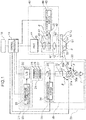
- the analysis device is provided with a chip holding portion 12 for holding an analysis chip 50; an excitation light emitting portion 20 for outputting excitation light onto the analysis chip 50 held on the chip holding portion 12; a light measuring portion 40 for measuring the intensity of light generated on the analysis chip 50; a control processor 14 (control portion) for controlling the respective constituent elements of the analysis device 10 such as the chip holding portion 12, the excitation light emitting portion 20, and the light measuring portion 40, and for performing various computations; and a display portion 16 for displaying various information such as computation results.
- the analysis device 10 is further provided with a pretreatment portion (not shown) for performing pretreatment of a blood sample from a patient.
- a sample solution is prepared by receiving a reagent chip (not shown) and by performing pretreatment (e.g. blood cell separation, dilution, mixing) of a blood sample injected to the reagent chip, and the sample solution is injected to the analysis chip 50.
- the reagent chip is formed with a number of storage units. A reagent, a dilluent, a cleaning solution and the like are individually packed in the storage units, in addition to a blood sample.
- the analysis chip 50 is provided with a prism 51, a metal film 55 formed on a surface of the prism 51, and a channel member 57 for forming a channel 58 along which a sample solution containing a specimen and a cleaning liquid are allowed to flow on the metal film 55 in contact with the metal film 55.
- Analysis chips 50 in the embodiment are replaced one after another, each time a specimen is detected (analyzed).
- the prism 51 includes, in the surfaces thereof, an incident surface 52 for allowing incidence of excitation light ⁇ from the excitation light emitting portion 20 into the prism 51, a deposition surface (predetermined surface) 53 having the metal film 55 formed thereon for reflecting the excitation light ⁇ entered to the prism 51, and an emission surface 54 from which the excitation light ⁇ reflected on the metal film 55 is outputted to the outside of the prism 51.
- the prism 51 is made of a transparent glass or resin.
- the emission surface 54 is a surface on which the excitation light ⁇ impinges for the first time after being reflected on the metal film 55.
- the emission surface 54 is formed on an optical surface of the prism in the same manner as the incident surface 52, so that light of the S-wave component of the excitation light ⁇ reflected on the metal film 55 does not stay in the prism 51.
- the prism 51 in the embodiment is made of a transparent resin having a refractive index of from about 1.4 to 1.6.
- the prism 51 may be made of glass. Further alternatively, the prism 51 may have such a shape that the incident surface 52, the deposition surface 53, and the emission surface 54 are included in the surfaces of the prism 51.
- the prism 51 may be of any shape, as far as the excitation light ⁇ entered from the incident surface 52 into the prism 51 is subjected to total reflection on the metal film 55 formed on the deposition surface 53, and the excitation light ⁇ (more specifically, the S-wave component of the excitation light ⁇ ) is outputted from the emission surface 54 without randomly reflecting and staying in the prism 51.
- the metal film 55 is a thin metal film deposited (formed) on the deposition surface 53 of the prism 51.
- the metal film 55 in the embodiment is made of gold.
- the metal film 55 is configured to amplify an evanescent wave (enhanced electric field), which is generated by causing the excitation light ⁇ to enter to the prism 51 while undergoing total reflection on the deposition surface 53, and by reflecting the entered excitation light ⁇ at a position of the deposition surface 53 where the metal film 55 is formed.
- the material of the metal film 55 is not limited to gold, but may be any metal that causes surface plasmon resonance.
- the metal film 55 may be made of silver, copper, or aluminum (including an alloy thereof).
- capturing bodies 56 for capturing a specific antigen are immobilized on a surface 55a of the metal film 55 (surface opposite from the side of the prism 51). These capturing bodies 56 are immobilized on the surface 55a of the metal film 55 by surface treatment.
- the channel member 57 is formed on the deposition surface 53 of the prism 51 (specifically, on the metal film 55), whereby the channel 58 along which a sample solution is allowed to flow is formed in cooperation with the deposition surface 53.
- the channel member 57 is made of a transparent resin.
- the channel member 57 is joined to the prism 51 by e.g. an adhesive agent, welding such as laser welding or ultrasonic welding, or clamping connection using a clamping member.
- the channel 58 has such a shape that the area where the metal film 55 is contacted with a sample solution is set larger than a measurement area by the light measuring portion 40.
- the sample solution subjected to pretreatment in the pretreatment portion is injected (supplied) to the channel 58. Then, after reaction of the capturing bodies 56 immobilized on the metal film 55 with the specimen (specific antigen) is finished, the analysis chip 50 carrying the sample solution is transported to the chip holding portion 12. Upon being transported to the chip holding portion 12, the analysis chip 50 is held on the chip holding portion 12 in a predetermined posture with respect to the analysis device 10.
- the chip holding portion 12 holds the analysis chip 50 thereon in such a manner that the analysis chip 50 is set in a predetermined posture with respect to the analysis device 10 in detecting a specimen.
- the predetermined posture is a posture that the excitation light ⁇ emitted from the excitation light emitting portion 20 enters the prism 51 from the incident surface 52 while undergoing total reflection on the deposition surface 53, and the entered excitation light ⁇ is reflected on the metal film 55.
- the chip holding portion 12 detachably holds the analysis chip 50.
- the chip holding portion 12 in the embodiment holds the analysis chip 50 thereon in such a manner that the prism 51 is located beneath the channel member 57.
- a light absorbent (not shown) is disposed near the emission surface 54 of the analysis chip 50 held on the chip holding portion 12 for keeping the light emitted from the emission surface 54 from being affected on the light measuring portion 40.
- the excitation light emitting portion 20 is configured to cause the excitation light ⁇ to enter the prism 51 in such a manner that the excitation light ⁇ is reflected on the metal film 55 of the prism 51 included in the analysis chip 50 held on the chip holding portion 12.
- the excitation light emitting portion 20 has a light source portion 21 for emitting linearly polarized excitation light, and an excitation optical system 30 for guiding the excitation light ⁇ emitted from the light source portion 21 to the incident surface 52 of the prism 51.
- the light source portion 21 has a light source unit 23 including an excitation light source 22, and a first wave-shaping portion 24 for shaping the excitation light ⁇ emitted from the excitation light source 22.
- the light source portion 21 in the embodiment downwardly emits the excitation light ⁇ .
- the excitation light source 22 in the embodiment is a laser diode.
- the light source unit 23 has the excitation light source 22, and a temperature adjusting circuit 25 for adjusting a temperature of the excitation light source 22.
- the light source unit 23 is configured to collimate the excitation light ⁇ emitted from the excitation light source 22, and to adjust and hold the posture of the excitation light source 22 in such a manner that the excitation light ⁇ enters the metal film 55 of the prism 51 from the minor axis side thereof. This is for the following reason.
- the temperature adjusting circuit 25 is a regression circuit for adjusting a temperature of the excitation light source (laser diode) 22. Specifically, the temperature adjusting circuit 25 monitors the light amount of light rays separated from light rays of excitation light ⁇ after collimation by e.g. a photodiode (not shown), whereby the temperature of the excitation light source 22 is adjusted to make the wavelength and the light amount of excitation light ⁇ to be emitted constant. The above operation is performed in view of a point that the wavelength and the emission energy of light to be emitted from the excitation light source 22 vary depending on temperatures.
- the first wave shaping portion 24 shapes the excitation light ⁇ emitted from the light source unit 23 by multiple filters (optical filters) so that the excitation light ⁇ has an excitation wavelength, at which the polarization direction is uniquely defined.
- the first wave shaping portion 24 has a first band-pass filter (hereinafter, simply called a "first BPF") 26, a linear polarization filter (hereinafter, simply called an "LPF") 27, and a first ND filter (hereinafter, simply called a "first NDF”) 28.
- the firs BPF 26 filters the emission light from the excitation light source 22 into light of a narrow wavelength band including only a center wavelength component, in view of a point that the emission light has a slight wavelength distribution range.
- the LPF 27 filters the emission light from the excitation light source 22 into linearly polarized light, in view of a point that the emission light has a slight difference in phase difference component.
- the first NDF 28 is a so-called neutral density filter. Specifically, the first NDF 28 dims the light emitted from the excitation light source 22 to thereby adjust the light amount of the excitation light ⁇ to be emitted from the light source portion 21. It should be noted that the first NDF 28 may be omitted from the first wave shaping portion 24 depending on an intensity of emission light to be emitted from the excitation light source 22.
- the excitation optical system 30 guides the excitation light ⁇ from the light source portion 21 to the prism 51 of the analysis chip 50 held on the chip holding portion 12.
- the excitation optical system 30 has a polarization direction adjusting portion 31 for changing the polarization direction of the excitation light ⁇ , a beam shaping optical system 32 for adjusting the contour or configuration of a beam of the excitation light ⁇ , and an incident path adjusting portion 35 for changing the incident path of the excitation light ⁇ into the prism 51 to thereby change the reflection position of the excitation light ⁇ on the metal film 55 or change an incident angle ⁇ of the excitation light ⁇ with respect to the metal film 55.
- the polarization direction adjusting portion 31 has a half wave plate 33, and a rotation driving portion 34 for rotating the half wave plate 33.
- the half wave plate 33 is disposed on the optical path of the excitation optical system 30, and is used as a polarization rotator for continuously rotating the polarization direction of the excitation light ⁇ .
- the rotation driving portion 34 is configured to rotate the polarization direction of the excitation light ⁇ with respect to the metal film 55 by rotating the half wave plate 33.
- the rotation driving portion 34 in the embodiment has a stepping motor, and is configured to rotate the half wave plate 33 by driving the stepping motor based on an instruction signal from the control processor 14. Rotating the half wave plate 33 as described above causes rotation of the polarization direction of the excitation light ⁇ which is linearly polarized by the first wave shaping portion 24.
- the amount of the P-wave component and the amount of the S-wave component of the excitation light ⁇ to be entered to the metal film 55 change.
- causing the rotation driving portion 34 to rotate the half wave plate 33 makes it possible to freely change the polarization direction from a condition in which an evanescent wave is maximally emerged from the metal film 55 (i.e. a condition in which the degree of enhancing the electric field to be formed near the surface 55a of the metal film 55 is maximized) to a condition in which emergence of evanescent wave is completely cut off (i.e. a condition in which an enhanced electric field is not formed at all near the surface 55a of the metal film 55).
- the beam shaping optical system 32 adjusts the beam size of the excitation light ⁇ or the contour or configuration of a beam, utilizing e.g. a slit or a zoom function so that the contour of the irradiation area of the excitation light ⁇ on the metal film 55 has a circular shape of a predetermined diameter.
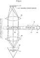
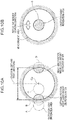
- the irradiation area of the excitation light ⁇ on the metal film 55 in the embodiment is adjusted to be smaller than the measurement area by the light measuring portion 40 (see FIG. 10B ).
- the incident path adjusting portion 35 has a reflective member 36 for reflecting the excitation light ⁇ from the light source portion 21, and a reflective member driving portion (driving portion) 37 for driving the reflective member 36.
- the reflective member 36 has a reflective surface 36a for reflecting the excitation light ⁇ thereon.
- the reflective member 36 in the embodiment is a reflection mirror.
- the reflective member 36 is constructed in such a manner that on the reflective surface 36a, there is deposited a dielectric multilayer film (specifically, a dielectric multilayer film in which both of the P-wave component and the S-wave component are deprived of wavelength dependence on the excitation light wavelength) in which phase displacement or dimming of light does not occur in excitation light ⁇ before incidence onto the reflective surface 36a, and in excitation light ⁇ after reflection on the reflective surface 36a.
- a dielectric multilayer film specifically, a dielectric multilayer film in which both of the P-wave component and the S-wave component are deprived of wavelength dependence on the excitation light wavelength
- a member made of a non-reflective light absorbing material capable of absorbing the excitation light ⁇ without reflecting the excitation light ⁇ is attached to a back surface 36b of the reflective member 36.
- the non-reflective light absorbing material include an absorption-type ND film and suede fabric.
- the reflective member driving portion 37 has a stage 37a, a rotation driving mechanism (not shown) which is disposed on the stage 37a and which is configured to drive and rotate the reflective member 36 while supporting the reflective member 36, and a reciprocation driving mechanism (not shown) for reciprocally driving the stage 37a.
- the rotation driving mechanism is configured to change the orientation of the reflective surface 36a by rotating the reflective member 36 (see the arrow ⁇ in FIG. 1 ). Specifically, the rotation driving mechanism supports the reflective member 36 in such a manner that the reflective surface 36a perpendicularly intersects a plane (the plane of FIG. 1 ) including the optical path of excitation light ⁇ to be entered to the reflective member 36, and the optical path of excitation light ⁇ after reflection on the reflective member 36.
- the rotation driving mechanism rotates the reflective member 36 based on an instruction signal from the control processor 14 in such a manner that the reflective surface 36a rotates along the plane including the optical paths, while maintaining the perpendicular posture of the reflective member 36 (posture that the reflective surface 36a perpendicularly intersects the plane including the optical paths).
- the rotation driving mechanism has a rotation motor, and changes the orientation of the reflective surface 36a by directly or indirectly driving and rotating the reflective member 36 by the rotation motor. Further, the rotation driving mechanism may rotate the reflective member 36 to such a position that the excitation light ⁇ from the light source portion 21 enters the back surface 36b of the reflective member 36, based on an instruction signal from the control processor 14.
- the reflective member 36 is mounted on the rotation driving mechanism at such a position that the centroid of the reflective member 36 passes near the center of rotation of the reflective member 36, and the rotation motor is configured to generate a sufficiently large torque.
- the rotation motor in the embodiment is a stepping motor having a high resolution.
- the rotation motor rotates the reflective member 36 at a predetermined angular interval (in other words, stepwise in the rotating direction), based on an instruction signal from the control processor 14.
- the predetermined interval is associated with the resolution for adjusting the orientation of the reflective surface 36a, and is set in accordance with the performance of the device, as necessary.
- the reciprocation driving mechanism linearly moves the stage 37a i.e. the reflective member 36 along the optical axis of the excitation light ⁇ from the light source portion 21 (see the arrow y in FIG. 1 ).
- the reciprocation driving mechanism in the embodiment reciprocally drives the stage 37a in the optical axis direction of the excitation light ⁇ from the light source portion 21, namely, in up and down directions.
- the reciprocation driving mechanism is configured to control the stepping motor by an instruction signal from the control processor 14, and the stage 37a carrying the rotation driving mechanism and the reflective member 36 thereon is reciprocally moved up and down by a screw feeding mechanism to be driven by the stepping motor.
- the reciprocation driving mechanism moves the reflective member 36 to a predetermined position on the optical axis with high precision in accordance with an instruction signal from the control processor 14, while maintaining the orientation of the reflective surface 36a with respect to the optical axis of the excitation light ⁇ from the light source portion 21.
- the light measuring portion 40 has a light receiving portion 41, a measurement optical system 42 for guiding light from the analysis chip 50 to the light receiving portion 41, and a second wave shaping portion 43 for shaping the light to be guided by the measurement optical system 42. Further, the light measuring portion 40 measures an intensity (in the embodiment, a light amount) of light to be generated on the metal film 55 of the analysis chip 50 and on a region adjacent to the metal film 55 (hereinafter, also simply called "light to be generated on the metal film 55").
- intensity in the embodiment, a light amount
- the light receiving portion 41 is configured to receive light and to output an intensity signal indicative of a light amount of the received light.
- a photomultiplier tube (PMT) having a high sensitivity and a high S/N ratio is used as the light receiving portion 41 for detecting weak light such as fluorescence to be generated by exciting a fluorescent material labeled on a specimen.
- the light receiving portion 41 is not limited to the PMT, but may be e.g. a cooling type CCD image sensor.
- the measurement optical system 42 is a conjugation optical system that is less likely to be affected by stray light, and has a condensing lens 44 and an image forming lens 45.
- the measurement optical system 42 in the embodiment is a two-lens-group conjugation optical system configured in such a manner that light travelling between two lens groups i.e. between the condensing lens 44 and the image forming lens 45 becomes parallel light or substantially parallel light.
- the second wave shaping portion 43 is configured to remove, from the light to be guided in the measurement optical system 42, an excitation light component (e.g. plasmon scattering light, Raman scattering light, or diffusion light) for adjusting the light amount (intensity) of light to be guided in the measurement optical system 42.
- the second wave shaping portion 43 has a second band-pass filter (first optical filter) 46, a second ND filter (second optical filter) 47, and a position switching portion 48 for switching the position of each of the filters 46 and 47.
- the second band-pass filter (hereinafter, simply called a "second BPF") 46 cuts off light at a wavelength (excitation wavelength) of the excitation light ⁇ .
- the second BPF 46 is capable of preventing incidence of light (e.g. leak light from the excitation light emitting portion 20, plasmon scattering light, or diffusion light) at a wavelength other than the wavelength of fluorescence (light generated by excitation of a fluorescent material labeled on a specimen by an enhanced electric field) onto the light receiving portion 41.
- the second BPF 46 removes a noise component from the light to be entered to the light receiving portion 41 to thereby improve detection precision and sensitivity of weak fluorescence by the light receiving portion 41.
- the second ND filter 47 (hereinafter, simply called a "second NDF") is a so-called neutral density filter, and is configured to emit light by attenuating the incident light.
- the second NDF 47 is capable of measuring e.g. plasmon scattering light by the light receiving portion (in the embodiment, PMT) 41 for detecting weak light (in the embodiment, fluorescence) by dimming e.g. plasmon scattering light or diffusion light to be guided in the measurement optical system 42.
- the light amount of light to be measured for obtaining an incident angle 61 of the excitation light ⁇ at which the enhanced electric field is maximized is significantly large, as compared with the light amount of excitation fluorescence to be measured in detecting a specimen.
- the second BPF 46 and the second NDF 47 are held on a common holding frame 49 in such a manner that the filters 46 and 47 are aligned on a certain plane substantially perpendicular to the optical axis (specifically, a plane substantially orthogonal to the optical axis of light travelling through the measurement optical system 42).
- the position switching portion 48 is configured to switch the position of each of the second BPF 46 and the second NDF 47 between a filtering position and a retracted position.
- the filtering position is a position on the optical path of the measurement optical system 42.
- the filtering position is a position at which each of the second BPF 46 and the second NDF 47 perpendicularly intersects the optical axis of parallel light or substantially parallel light between the condensing lens 44 and the image forming lens 45, and crosses the parallel light or the substantially parallel light, between the condensing lens 44 and the image forming lens 45.
- the analysis device 10 is operable to precisely detect a specimen. In other words, if the second BPF 46 or the second NDF 47 is inclined with respect to the optical axis of e.g. parallel light travelling between the condensing lens 44 and the image forming lens 45, the optical axis of light passing through the second BPF 46 or through the second NDF 47 is shifted. This may lower the measurement precision by the light measuring portion 40.
- the retracted position is a position deviated from the optical path of the measurement optical system 42.
- the position switching portion 48 switches the position of each of the second BPF 46 and the second NDF 47 in such a manner that when the second BPF 46 is in the filtering position, the second NDF 47 is set to the retracted position (see FIG. 4 ), and when the second BPF 46 is in the retracted position, the second NDF 47 is set to the filtering position.
- the position switching portion 48 in the embodiment is configured to switch the position of each of the second BPF 46 and the second NDF 47 by reciprocally moving the holding frame 49 along a plane on which the filters 46 and 47 are aligned (see the arrow ⁇ in FIG. 4 ). By performing the switching operation as described above, the operations of switching the positions of the two filters 46 and 47 are simultaneously performed by one drive source.
- the position switching portion 48 performs the operation of switching the position of each of the filters 46 and 47 in accordance with an instruction signal from the control processor 14.
- the second wave shaping portion 43 in the embodiment is provided with the second BPF 46 and the second NDF 47.
- the invention is not limited to the above.
- the second NDF 47 may be omitted from the second wave shaping portion 43.
- the second NDF 47 may also be omitted, in the case where the analysis device has a configuration of switching between light receiving portions depending on light to be measured, specifically, in the case where the analysis device has a configuration of switching between a light receiving portion 41 for receiving fluorescence, and another light receiving portion for receiving light having a larger light amount than the light amount of fluorescence.
- the operation of switching the position of each of the filters 46 and 47 is performed by reciprocally moving the holding frame 49 by the position switching portion 48.
- a disc-shaped holding frame may individually holds the second BPF 46 and the second NDF 47 in such a manner that the filters 46 and 47 are aligned on one plane, and a position switching portion may rotate the disc-shaped holding frame about an intermediate position between the second BPF 46 and the second NDF 47 as a center of rotation.
- a position switching portion may have two drive sources, so that switching of the position of the second BPF 46 and switching of the position of the second NDF 47 are individually carried out by the two drive sources.
- the control processor 14 controls each of the constituent elements constituting the analysis device 10. For instance, in the case where the analysis device 10 analyzes a specimen, the control processor 14 controls the light source portion 21, the polarization direction adjusting portion 31, the incident path adjusting portion 35, and the light measuring portion 40. By performing the above controls, the analysis device 10 is operable to perform e.g. a resonance angle scanning process, an optimum position scanning process, a birefringence measuring process, and an excitation fluorescence measuring process. Further, in the case where a specimen is analyzed, the control processor 14 is operable to perform computations based on an output signal to be transmitted from the light measuring portion 40 (specifically, the light receiving portion 41) for analyzing fluorescence measured by the light measuring portion 40.
- the analysis device 10 is operable to perform e.g. a resonance angle scanning process, an optimum position scanning process, a birefringence measuring process, and an excitation fluorescence measuring process.
- the control processor 14 is operable to perform computations based on an output signal to
- control processor 14 counts the number of fluorescent particles per unit area detected by the light measuring portion 40, and calculates an increase of fluorescence with time.
- a computation result by the control processor 14 is outputted to the display portion 16 which is connected to the control processor 14. The details on concrete control operations and computations by the control processor 14 are described later.
- the display portion 16 displays a computation result by the control processor 14, based on an output signal from the control processor 14.
- the display portion 16 may be a liquid crystal display which is configured to display a computation result on a screen, or may be a printer which is configured to print out a computation result. Further alternatively, the display portion 16 may be a combination of a device for displaying a screen and a device for printing out a computation result.
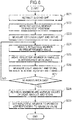
- FIG. 5 is a flowchart showing a basic sequence to be performed in analyzing a specimen by the analysis device 10.
- FIG. 6 is a flowchart showing a resonance angle scanning sequence.
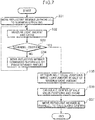
- FIG. 7 is a flowchart showing an optimum position scanning sequence.
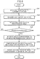
- FIG. 8 is a flowchart showing a birefringence measuring sequence.
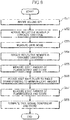
- FIG. 9 is a flowchart showing an excitation fluorescence measuring sequence.
- a blood sample is supplied from a patient, and the supplied blood sample is injected to a reagent chip.
- the reagent chip containing the blood sample is placed in the pretreatment portion of the analysis device 10.
- the control processor 14 controls the pretreatment portion to perform pretreatment (e.g. blood cell separation, dilution, mixing) of the blood sample contained in the reagent chip placed in the pretreatment portion, whereby a sample solution is prepared.
- pretreatment e.g. blood cell separation, dilution, mixing
- the control processor 14 controls the pretreatment portion to flow the sample solution subjected to the pretreatment into the channel 58 of the analysis chip 50 for capturing a specimen (specific antigen) by the capturing bodies 56 immobilized on the surface of the metal film 55.
- the pretreatment portion reacts the capturing bodies 56 with the specimen.
- the capturing bodies 56 capture a specimen labeled by a fluorescent material (in the embodiment, a fluorescent pigment).
- a fluorescent material may be injected to the analysis chip 50 to thereby label the specimen in a state that the fluorescent material is captured by the capturing bodies 56.
- the analysis chip 50 which has undergone the above reaction is transported to the chip holding portion 12, and held on the chip holding portion 12 (Step S1).
- the excitation light source 22 (in the embodiment, a laser diode) 22 is kept in a constant temperature condition by being constantly subjected to temperature adjustment by the temperature adjusting circuit 25 for outputting output light of a stable wavelength with less wavelength variation.
- the above operation is essential in a device configured to quantitatively determine e.g. the proteins in a blood sample, because wavelength variation causes a change of the surface plasmon resonance condition or a change of the emerging amount of evanescent wave (enhanced electric field). It takes a certain time to obtain a certain maintenance temperature. Therefore, it is a normal practice that the excitation light source 22 is kept in a certain temperature range by the temperature adjusting circuit 25 from the point of time when the power source of the analysis device 10 is turned on.
- the control processor 14 In response to placing the analysis chip 50 on the chip holding portion 12, the control processor 14 performs scanning of an optimum surface plasmon resonance condition (scanning of a resonance angle) with respect to the analysis chip 50. Then, the control processor 14 performs positioning (first positioning) of the reflective member 36, based on the scanning result, so that the excitation light ⁇ enters the metal film 55 at the incident angle (excitation incident angle ⁇ 1) at which the electric field intensity of an enhanced electric field to be generated on the metal film 55 is maximized (Step S2).
- the control processor 14 controls the reflective member driving portion 37 to drive the reflective member 36 to thereby scan the incidence condition (excitation incident angle ⁇ 1) of the excitation light ⁇ with respect to the metal film 55 of the prism 51 included in the analysis chip 50.
- the incident angle ⁇ 1 of excitation light at which the intensity of an enhanced electric field (evanescent wave) on the metal film 55 of the prism 51 based on surface plasmon resonance is maximized is determined by e.g. the material and the shape of the prism 51 to be included in the analysis chip 50, or by the refractive index of a channel filling liquid (sample solution). Nevertheless, the excitation light incidence condition (excitation incident angle ⁇ 1) fluctuates by e.g.
- the control processor 14 causes the excitation light ⁇ to enter the metal film 55 at an incident angle in the range of less than ⁇ 10° with respect to an excitation incident angle ⁇ 1a based on design. Then, an excitation incident angle ⁇ 1 with respect to the analysis chip 50 is obtained, based on the light amount of light to be generated on the metal film 55 at the time of light incidence.
- the control processor 14 controls the position switching portion 48 of the second wave shaping portion 43 to move the second BPF 46 to the retracted position, and to move the second NDF 47 to the filtering position (Step S21).
- the half wave plate 33 of the polarization direction adjusting portion 31 is in an ideal state in terms of design (initial state), in which the P-wave component of the excitation light ⁇ to be entered to the metal film 55 that is irradiated with the excitation light ⁇ from the excitation light emitting portion 20 is maximized.
- the control processor 14 controls the rotation driving mechanism and the reciprocation driving mechanism of the reflective member driving portion 37 to move the reflective member 36 to a farthest position (Step S22).
- the farthest position is a position of the reflective member 36 and an orientation of the reflective surface 36a, corresponding to an incident angle ⁇ , at which an evanescent wave does not emerge in a region near the surface 55a of the metal film 55 in a state that the excitation light ⁇ emitted from the excitation light emitting portion 20 is reflected on a specific position on the metal film 55 (in the embodiment, within the measurement area of the light measuring portion 40).
- the control processor 14 controls the light measuring portion 40 to measure the light amount of light generated on the metal film 55. Then, the control processor 14 acquires the measurement result of the light measuring portion 40 by an output signal from the light measuring portion 40 (specifically, the light receiving portion 41).
- the light to be measured by the light measuring portion 40 when the reflective member 36 is in the farthest position is surface diffusion light SK from the prism 51.
- the control processor 14 stores the incident angle ⁇ of the excitation light ⁇ with respect to the metal film 55, and the light amount of light measured by the light measuring portion 40 in correlation with each other (Step S23). Since the second BPF 46 is in the retracted position when the above operation is performed, the light to be received by the light receiving portion 41 includes light of a same wavelength as the excitation wavelength of the excitation light ⁇ .
- the light of the same wavelength as the excitation wavelength includes plasmon scattering light, Raman scattering light, and diffusion light generated on the metal film 55. These lights of the same wavelength as the excitation wavelength are enhanced by surface plasmon resonance generated on the metal film 55.
- the light amount of light of the same wavelength as the excitation wavelength is sufficiently large, as compared with the light amount of excitation fluorescence generated by excitation of a fluorescent material labeled on a specimen.
- causing the control processor 14 to control the position switching portion 48 to retract the second BPF 46 from the optical path of the measurement optical system 42 for allowing the light receiving portion 41 to receive the light of the excitation wavelength is advantageous in precisely measuring the light amount of light to be generated on the metal film 55.
- the light receiving portion 41 for measuring excitation fluorescence of a small light amount is configured to measure e.g. surface plasmon scattering light or diffusion light, whose light amount is significantly larger than the light amount of excitation fluorescence.
- the analysis device 10 is configured to cause the position switching portion 48 to retract the second BPF 46 to the retracted position and to move the second NDF 47 to the filtering position, whereby the common light receiving portion (in the embodiment, PMT) 41 is capable of measuring the light amounts of both lights (e.g. scattering light and excitation fluorescence).
- the control processor 14 controls the incident path adjusting portion 35 to adjust the position of the reflective member 36 in a state that the excitation light ⁇ is emitted from the light source portion 21. Specifically, the control processor 14 controls the rotation driving mechanism to rotate the orientation of the reflective surface 36a (Step S24), and controls the reciprocation driving mechanism to move the position of the reflective member 36 (Step S25), while keeping the irradiation position of the excitation light ⁇ from being displaced on the metal film 55.
- control processor 14 stores in advance in a table in correlation with each other, each respective position of the reflective member 36, and each respective orientation of the reflective surface 36a at which the excitation light ⁇ reflected on the reflective surface 36a enters the prism 51 and impinges a specific position on the metal film 55 in a state that the reflective member 36 is positioned at each respective position. Then, the control processor 14 controls the rotation driving mechanism and the reciprocation moving mechanism to move the reflective member 36, based on the table.
- Step S24 and Step S25 may be performed prior to the other of Step S24 and Step S25, and then, the other of Step S24 and Step S25 may be performed; or both of Step S24 and Step S25 may be performed simultaneously.
- the light measuring portion 40 measures the light amount of light generated on the metal film 55 and outputs the measurement result by the light measuring portion 40 to the control processor 14, and the control processor 14 stores the measurement result in correlation with the incident angle ⁇ (Step S26).
- control processor 14 controls the light measuring portion 40 to measure the light amount of light while changing the incident angle ⁇ in such a manner that the irradiation position on the metal film 55 is not displaced, and stores the measurement result by the light measuring portion 40.
- the control processor 14 controls the light measuring portion 40 to measure the light amount of light in a predetermined scanning area (e.g. at the incident angle ⁇ in the range of less than ⁇ 10° with respect to the excitation incident angle ⁇ 1a based on design), and thereafter, controls the light source portion 21 to stop the emission of the excitation light ⁇ from the light source portion 21 (Step S27). Then, the control processor 14 retrieves a maximum value and a minimum value among the stored light amounts, and stores the retrieved maximum and minimum values (Step S28).
- a predetermined scanning area e.g. at the incident angle ⁇ in the range of less than ⁇ 10° with respect to the excitation incident angle ⁇ 1a based on design
- control processor 14 controls the reflective member driving portion 37 to drive the reflective member 36 so that the position of the reflective member 36 and the orientation of the reflective surface 36a respectively coincide with the position of the reflective member 36 and with the orientation of the reflective surface 36a at which the maximum amount of light was obtained (Step S29).
- control processor 14 After the first positioning of the reflective member 36 is completed, the control processor 14 performs positioning (second positioning) of the reflective member 36 so that the irradiation position (incident position) of the excitation light ⁇ onto the metal film 55 coincides with a center portion of the measurement area by the light measuring portion 40 (Step S3).
- the control processor 14 controls the reciprocation driving mechanism of the reflective member driving portion 37 to move the reflective member 36 to an upper end position (Step S31).
- the upper end position is a position, where the incident position of the excitation light ⁇ on the metal film 55 lies on the outside of the measurement area by the light measuring portion 40 (see the position A in FIG. 10A ).
- the control processor 14 controls the light source portion 21 to emit the excitation light ⁇ when the reflective member 36 lies in an area including the above position, controls the light measuring portion 40 to measure the light amount of light generated on the metal film 55 at the time of incidence of the excitation light ⁇ , and stores the measurement result by the light measuring portion 40 (Step S32).
- the control processor 14 determines whether the reflective member 36 is in the lower end position (Step S33). The details on the lower end position will be described later. In the case where it is determined that the reflective member 36 is not in the lower end position, the control processor 14 controls the reciprocation driving mechanism to move the reflective member 36 downward by a predetermined amount (Step S34). When the above control is performed, the control processor 14 controls only the reciprocation driving mechanism to move the reflective member 36, without controlling the rotation driving mechanism to rotate the reflective member 36. In other words, the control processor 14 moves only the position of the reflective member 36, without changing the orientation of the reflective surface 36a with respect to the excitation light ⁇ from the light source portion 21.
- the control processor 14 controls the light source portion 21 to emit excitation light, controls the light measuring portion 40 to measure the light amount of light generated on the metal film 55 at the time of emitting the excitation light, and stores the measurement result by the light measuring portion 40 (Step S32). Then, the control processor 14 determines whether the reflective member 36 is in the lower end position (Step S33). The control processor 14 repeats Step S32 through Step S34 in this order until the reflective member 36 is moved to the lower end position.
- the control processor 14 determines whether the reflective member has reached the lower end position based on a judgment as to whether a light amount i.e. a measurement result by the light measuring portion 40 has decreased by 50% of the maximum amount of light among the stored light amounts. Specifically, the light amount to be measured by the light measuring portion 40 at the beginning of measurement is small, because the irradiation area of the excitation light ⁇ on the metal film 55 is on the outside of the measurement area by the light measuring portion 40 at the beginning of the measurement. As the reflective member 36 is gradually moved downward, and the irradiation area of the excitation light ⁇ begins to fall in the measurement area by the light measuring portion 40 (see the position B in FIG. 10A ), the light amount of light to be measured by the light measuring portion 40 gradually increases.
- the reflective member 36 When the reflective member 36 is further moved downward, and the entirety of the irradiation area of the excitation light ⁇ completely falls in the measurement area by the light measuring portion 40 (see the position C in FIG. 10A ), the light amount of light on the metal film 55 to be measured by the light measuring portion 40 becomes maximum.
- the reflective member 36 is furthermore moved downward, the irradiation area of the excitation light ⁇ is moved to the outside of the measurement area by the light measuring portion 40, from the side of the measurement area opposite from the incident side of the measurement area (see the position D in FIG. 10A ).
- the light amount of light to be measured by the light measuring portion 40 decreases. In other words, lens vignetting (light falloff at edge portions) occurs.
- the control processor 14 stores the intensities of the lights, and the up and down positions of the reflective member 36 when the respective intensities are measured in correlation with each other, and determines whether the light amount of the measured light decreases by 50% of the maximum amount of light. Then, the control processor 14 determines that the reflective member 36 has reached the lower end position when the light amount of light to be measured by the light measuring portion 40 has decreased by 50% of the maximum amount of light.
- the control processor 14 determines that the reflective member 36 has moved to the lower end position, the control processor 14 retrieves a value at which the light amount has decreased by 50% of the maximum amount of light, among the values of the stored light amounts (Step S35). There are two values to be retrieved (see the position B and the position D in FIG. 10A ). The control processor 14 retrieves each of the positions of the reflective member 36 at which the light amount of light to be measured by the light measuring portion 40 decreased by 50% of the maximum amount of light. Then, the control processor 14 calculates a center position (see the position Ce in FIG. 10A ) between the two positions, and stores the calculated center position (Step S36). The control processor 14 controls the reciprocation driving mechanism to move the reflective member 36 for moving the irradiation position to the calculated center position Ce (Step S37: see FIG. 10B ).
- self fluorescence By performing the above control, it is possible to make the light amount of self fluorescence constant, each time the analysis chip 50 is measured by the light measuring portion 40. Specifically, fluorescence generates in the prism 51 due to the excitation light ⁇ travelling through the prism 51 (self fluorescence). Such self fluorescence is weak, as compared with scattering light (such as plasmon scattering light or diffusion light) generated on the metal film 55. However, in the case where the concentration of a specimen in a sample solution is low, self fluorescence may have substantially the same intensity as the excitation fluorescence emitted from a fluorescent material labeled on the specimen. As a result, the self fluorescence may turn out to be noise in measuring excitation fluorescence.
- Birefringence occurs when the excitation light ⁇ travels through the prism 51.
- the control processor 14 measures the birefringence (Step S4). Taking into account the birefringence to be measured by the control processor 14 in measuring excitation fluorescence from a fluorescent material labeled on a specimen is advantageous in improving the precision in measuring a specimen.
- birefringence occurs when light is transmitted through a medium. Birefringence increases in the case where light is transmitted through a dielectric body such as a resin member. The birefringence occurs due to e.g. a density difference among media, and the density difference occurs when the media are formed. Therefore, the degree of birefringence differs among individual prisms 51.
- Phase rotation is generated in the excitation light ⁇ travelling through the prism 51 by birefringence, and an S-wave component may be generated in the excitation light ⁇ by phase rotation resulting from the birefringence, regardless of an intention to enter only a P-wave component onto the metal film 55.
- the light amount of excitation fluorescence excited in an enhanced electric field decreases depending on the amount of the S-wave component generated by the birefringence. Accordingly, causing the control processor 14 to correct the light amount by the decreased amount is advantageous in improving detection precision and sensitivity of a specimen by the analysis device 10.
- the control processor 14 controls the light source portion 21 to emit the excitation light ⁇ , and controls the light measuring portion 40 to measure the light amount of light generated on the metal film 55.
- the half wave plate 33 is set in an initial state (Step S41).
- the control processor 14 stores the light amount of light measured by the light measuring portion 40 in correlation with the rotation position of the half wave plate 33 (a rotation angle with respect to the initial state), while controlling the rotation driving portion to rotate the half wave plate 33 (Step S42 and Step S43).
- Rotating the half wave plate 33 by the control processor 14 respectively increases and decreases the P-wave component and the S-wave component of the excitation light ⁇ to be entered to the metal film 55.
- the light amount of light to be measured by the light measuring portion 40 increases and decreases.
- an increase in the P-wave component of the excitation light ⁇ results in a decrease in the S-wave component
- a decrease in the P-wave component of the excitation light ⁇ results in an increase in the S-wave component.
- the P-wave component of the excitation light ⁇ to be entered to the metal film 55 increases, the light amount of light to be measured by the light measuring portion 40 increases.
- the S-wave component increases, the light amount of light to be measured by the light measuring portion 40 decreases. This is because the P-wave component contributes to surface plasmon resonance, but the S-wave component does not contribute to surface plasmon resonance.
- the control processor 14 repeats Step S42 and Step S43 in this order until a maximum value DRmax and a minimum value DRmin of the light amount of light to be measured by the light measuring portion 40 are obtained (Step S44). Then, upon acquiring the maximum value DRmax and the minimum value DRmin, the control processor 14 retrieves the maximum value DRmax and the minimum value DRmin, from the stored light amounts and the stored rotation positions of the half wave plate 33, (Step S45), retrieves the rotation positions of the half wave plate 33 when the respective values are retrieved (specifically, a first rotation position when the maximum value DRmax is obtained, and a second rotation position when the minimum value DRmin is obtained), and stores the retrieved values and the retrieved rotation positions.
- control processor 14 derives a major axis rotation amount ⁇ i by birefringence in the prism 51, and a correction coefficient K, based on the formula (1) and the formula (2), using the stored maximum value DRmax, the stored minimum value DRmin, and the light amount of surface diffusion light SK that is stored in the resonance angle scanning process, and stores the derived major axis rotation amount ⁇ i and the derived correction coefficient K (Step S46).
- control processor 14 controls the rotation driving portion 34 to rotate the half wave plate 33 to the rotation position at which the maximum value DRmax was obtained.
- the excitation light ⁇ is caused to enter the metal film 55 in a state that the P-wave component is largest (in other words, in a state that the S-wave component is smallest).
- the control processor 14 controls the light source portion 21 to irradiate the excitation light ⁇ onto the reflective member 36 which has undergone the first positioning and the second positioning.
- the excitation light ⁇ causes surface plasmon resonance on the metal film 55.
- the fluorescent material labeled on the specimen and captured by the capturing bodies 56 on the metal film 55 is excited by the enhanced electric field based on the surface plasmon resonance, whereby fluorescence (excitation fluorescence) is emitted.
- the control processor 14 controls the light measuring portion 40 to measure the excitation fluorescence (Step S5).
- the control processor 14 controls the position switching portion 48 to move the second BPF 46 to the filtering position, and to retract the second NDF 47 to the retracted position (Step S51: see FIG. 1 and FIG. 4 ). Then, the control processor 14 controls the rotation driving mechanism of the reflective member driving portion 37 to rotate the reflective member 36 to such a position that the excitation light ⁇ emitted from the light source portion 21 enters the non-reflective light absorbing material on the back surface 36b of the reflective member 36 (Step S52). By performing the above control, the prism 51 is brought to a state that the excitation light ⁇ is not incident.
- the control processor 14 controls the light measuring portion 40 to perform a measurement, and stores an output (dark noise DN) from the light measuring portion 40 (Step S53). Then, the control processor 14 controls the rotation driving mechanism of the reflective member driving portion 37 to rotate the reflective member 36 to such a position that the excitation light ⁇ from the light source portion 21 enters the reflective surface 36a of the reflective member 36 (Step S54).
- the orientation of the reflective surface 36a in the above state is the orientation defined in Step S29 of the resonance angle scanning process.
- the control processor 14 controls the light source portion 21 to emit the excitation light ⁇ , controls the light measuring portion 40 to measure the light amount of excitation fluorescence resulting from an enhanced field generated near the metal film 55, and stores the measurement result by the light measuring portion 40 (Step S55).
- the control processor 14 obtains a measurement maximum amount of light (first light amount value) Smax.
- the measurement maximum amount of light is obtained because the half wave plate 33 is rotated to the first rotation position obtained in the birefringence measuring process (in other words, the rotation position at which the light amount of light to be generated on the metal film 55 irradiated with the excitation light ⁇ is equal to the maximum value DRmax), and the intensity of the enhanced electric field near the metal film 55 is largest.
- the control processor 14 controls the rotation driving portion 34 to rotate the half wave plate 33 to the second rotation position obtained in the birefringence process (i.e. the rotation position at which the light amount of light to be generated on the metal film 55 irradiated with the excitation light ⁇ is equal to the minimum value DRmin) (Step S56). Then, the control processor 14 controls the light measuring portion 40 to measure the light amount of the excitation fluorescence, and stores the measurement result by the light measuring portion 40 (Step S57). By performing the above control, the control processor 14 obtains a measurement minimum light amount (second light amount value) Smin.
- the control processor 14 derives a light amount h of the self fluorescence by the prism and a light amount H of the excitation fluorescence, as expressed by the following formulas (3-1) through (8), using the stored measurement maximum amount of light Smax, the stored measurement minimum light amount Smin, and the stored dark noise DN; and stores the derived values (Step S58).
- H1 is the light amount of excitation fluorescence and h1 is the light amount of self fluorescence when Smax was obtained
- H2 is the light amount of excitation fluorescence and h2 is the light amount of self fluorescence when Smin was obtained.
- the control processor 14 obtains the light amount H of excitation fluorescence, using the following approximation formula (9).
- H S max ⁇ S min 2 ⁇ DN 2
- control processor 14 obtains the light amount H of excitation fluorescence, using the following approximation formula (10).
- H S max ⁇ S min 2
- the control processor 14 stores the true light amount H in association with the specimen number (Step S6). Then, the control processor 14 erases the data other than the above. Further, the control processor 14 outputs, to the display portion 16, information based on the light amount H of excitation fluorescence that is stored in association with the specimen number. The display portion 16 displays the information based on the light amount H.
- control processor 14 returns the reflective member 36 to the initial position (Step S7), and the sequence of measurements is finished.
- the incident angle ⁇ of the excitation light ⁇ with respect to the metal film 55 can be changed by driving the reflective member 36. Accordingly, it is possible to suppress displacement of the reflection position of the excitation light ⁇ on the metal film 55 resulting from a change in the incident angle ⁇ .
- the incident angle ⁇ of the excitation light ⁇ with respect to the metal film 55 is changed by changing and adjusting the position of the reflective member 36 and the orientation of the reflective surface 36a. Accordingly, unlike a conventional configuration, in which the incident angle ⁇ is adjusted by moving the entirety of an excitation optical system constituted of a light source and lenses, the above configuration is advantageous in suppressing the number of movable components and the weight of a movable portion.
- the analysis device 10 is operable to generate an enhanced electric field based on surface plasmon resonance in the vicinity of the metal film 55 by causing one excitation light ⁇ to enter the prism 51.
- This is advantageous in preventing an increase in the light amount of self fluorescence, which may occur in a conventional configuration, in which multiple excitation lights ⁇ , ⁇ , ... having different incident angles ⁇ are caused to simultaneously enter the prism 51.
- the above configuration is advantageous in suppressing lowering of the S/N ratio of a signal to be obtained by measuring light generated near the metal film 55 by surface plasmon resonance due to self fluorescence.
- the incident angle ⁇ of the excitation light ⁇ with respect to the metal film 55 is precisely set in such a manner that the electric field intensity of an enhanced electric field by surface plasmon resonance is maximized.
- the absorption peak of reflection light on the metal film 55 in angle spectroscopy, and the peak of the electric field intensity of the enhanced electric field are displaced from each other, the peak of intensity of light (light to be generated on the metal film 55) to be generated resulting from surface plasmon resonance coincides with the peak of the electric field intensity of the enhanced electric field.
- adjusting the reflective member 36 in such a manner that the position of the reflective member 36 and the orientation of the reflective surface 36a respectively coincide with the position of the reflective member 36 and with the orientation of the reflective surface 36a at which the light amount of light to be generated on the metal film 55 is maximized enables to set the incident angle of the excitation light ⁇ with respect to the metal film 55 to be equal to the excitation incident angle ⁇ 1 at which the electric field intensity of the enhanced electric field is maximized.
- the half wave plate 33 is adjusted so that the polarization direction of the excitation light coincides with the rotation position of the half wave plate 33, at which the S-wave component is maximized at the time of reflection on the metal film 55. Then, by measuring the excitation fluorescence in the above state by the light measuring portion 40, the light amount of self fluorescence from the prism 51 is obtained. By performing the above control, it is possible to remove the influence of self fluorescence, from a measurement result of excitation fluorescence by the light measuring portion 40, in the case where the half wave plate 33 is adjusted and the P-wave component is maximized at the time of incidence of polarized excitation light ⁇ onto the metal film 55. This enables to extract excitation fluorescence.
- the analysis device 10 is operable to precisely detect excitation fluorescence, while suppressing an influence of self fluorescence. This is advantageous in securing a wide dynamic range.
- the embodiment it is possible to detect a specimen with high sensitivity and with high precision. Specifically, by measuring a light amount of light to be generated on the metal film 55 by surface plasmon resonance, it is possible to precisely obtain the incident angle (excitation incident angle) ⁇ 1 of the excitation light ⁇ with respect to the film 55, at which the intensity of an enhanced electric field to be formed near the surface 55a of the metal film 55 is maximized.
- light to be generated on the metal film 55 is light of an excitation wavelength such as plasmon scattering light or surface diffusion light.
- the second BPF 46 is inserted on the optical path of the measurement optical system 42, whereby the light component of the excitation wavelength such as plasmon scattering light or surface diffusion light is removed from the light to be measured by the light measuring portion 40.
- analysis chips 50 are replaced one after another, each time a specimen is detected.
- the invention is not limited to the above.
- the analysis device 10 may be configured in such a manner that an analysis chip is incorporated in a part of the analysis device 10 and detections of specimens are performed by repeatedly using the one analysis chip.
- control processor 14 measures an intensity of light to be generated on the metal film 55 while continuously changing the incident angle 6 of the excitation light ⁇ with respect to the metal film 55 in obtaining the excitation incident angle 61.
- the invention is not limited to the above.
- control processor 14 may perform a first scanning operation of measuring a light amount of light to be generated on the metal film 55 at each respective incident angle 6 while intermittently changing the incident angle 6 (e.g. at an interval of 1° of the incident angle) in a first range, and may perform a second scanning operation of measuring a light amount of light to be generated on the metal film 55 while intermittently or continuously changing the incident angle ⁇ so that the interval of the incident angle ⁇ is set smaller than that in the first scanning operation (e.g. at an interval of 0.1° of the incident angle) in a second range based on the result of the first scanning operation.
- control processor 14 may define the second range based on the first scanning operation, using a discrete step, and thereafter, may obtain the excitation incident angle ⁇ 1, at which the light amount of light to be generated on the metal film 55 is equal to the maximum amount of light by finely scanning in the thus defined second range. It should be noted that the second range is included in the first range.
- the control processor 14 changes the incident angle ⁇ at an interval of 1° in a range (first range) of the incident angle 6 of less than ⁇ 10° with respect to the excitation incident angle ⁇ 1a based on design.
- the control processor 14 measures a light amount of light to be generated on the metal film 55 at each respective incident angle ⁇ (first scanning operation), and stores the measurement result in association with a corresponding incident angle 6.
- the control processor 14 changes the incident angle ⁇ at an interval of 0.1° in a range (second range) of the incident angle 6 of ⁇ 1° or less with respect to the incident angle 6, at which the maximum amount of light was obtained by the first scanning operation, or continuously changes the incident angle 6.
- the control processor 14 measures a light amount of light to be generated on the metal film 55 (second scanning operation), and stores the measurement result in association with a corresponding incident angle ⁇ . Then, the control processor 14 defines the incident angle 6 at which the maximum amount of light was obtained, as the excitation incident angle 61 in the second scanning operation.
- the above configuration is advantageous in efficiently determining the excitation incident angle 61 at which the enhanced electric field is maximized, as compared with a configuration in which the overall of the first range is finely scanned.
- the first scanning operation and the second scanning operation are performed in the resonance angle scanning process, and the analysis device 10 sequentially analyzes specimens, while holding analysis chips 50 one after another on the chip holding portion 12, the first scanning operation may be performed only for a first analysis chip 50, and only the second scanning operation may be performed for a second analysis chip 50 and thereafter.
- the control processor 14 changes, with respect to the first analysis chip 50, the incident angle ⁇ at an interval of 1° in a range (first range) of the incident angle ⁇ of less than ⁇ 10° with respect to the excitation incident angle ⁇ 1a based on design.
- the control processor 14 measures a light amount of light to be generated on the metal film 55 at each respective incident angle ⁇ (first scanning operation), and stores the measurement result in association with a corresponding incident angle ⁇ .
- the control processor 14 changes the incident angle ⁇ at an interval of 0.1° in a range (second range) of the incident angle 6 of ⁇ 3° or less with respect to the incident angle ⁇ , at which the maximum amount of light was obtained in the first scanning operation, or continuously changes the incident angle ⁇ .
- the control processor 14 measures a light amount of light to be generated on the metal film 55 (second scanning operation), and stores the measurement result in association with a corresponding incident angle ⁇ . Then, the control processor 14 defines the incident angle ⁇ at which the maximum amount of light was obtained in the second scanning operation, as the excitation incident angle ⁇ 1 with respect to the first analysis chip 50.
- the control processor 14 changes, with respect to the second analysis chip 50, the incident angle ⁇ at an interval of 0.1° in the second scanning range obtained by the first scanning operation with respect to the first analysis chip 50, or continuously changes the incident angle ⁇ , without performing the first scanning operation.
- the control processor 14 measures a light amount of light to be generated on the metal film 55 (second scanning operation), and stores the measurement result in association with a corresponding incident angle ⁇ .
- the control processor 14 defines the incident angle 6 at which the maximum amount of light was obtained in the second scanning operation, as the excitation incident angle ⁇ 1 with respect to the second analysis chip 50.
- the control processor 14 performs only the scanning operation (second scanning operation) in the second range which was obtained with respect to the first analysis chip 50. This is advantageous in shortening the analysis time.
- the surface plasmon resonance fluorescence analysis device is a surface plasmon resonance fluorescence analysis device for measuring fluorescence emitted by excitation of a fluorescent material labeled on a specimen by an electric field based on surface plasmon resonance.
- the surface plasmon resonance fluorescence analysis device includes a chip holding portion which is configured to detachably hold an analysis chip including a prism having a metal film formed on a predetermined surface thereof; a light source portion which emits excitation light for causing surface plasmon resonance on the metal film; and an incident path adjusting portion which allows the excitation light to enter the prism of the analysis chip held on the chip holding portion by reflection of the excitation light emitted from the light source portion.
- the incident path adjusting portion includes a reflective member having a reflective surface formed thereon for reflecting the excitation light from the light source portion, and a driving portion for driving the reflective member.
- the driving portion is configured to change a position of the reflective member and to adjust an orientation of the reflective surface in such a manner that the excitation light entered the prism is reflected at a specific position on the metal film.
- a surface plasmon resonance fluorescence analysis device for measuring fluorescence emitted by excitation of a fluorescent material labeled on a specimen by an electric field based on surface plasmon resonance.
- the surface plasmon resonance fluorescence analysis device includes a prism having a metal film formed on a predetermined surface thereof; a light source portion which emits excitation light for causing surface plasmon resonance on the metal film; and an incident path adjusting portion which allows the excitation light to enter the prism by reflection of the excitation light emitted from the light source portion.
- the incident path adjusting portion may include a reflective member having a reflective surface formed thereon for reflecting the excitation light from the light source portion, and a driving portion for driving the reflective member.
- the driving portion may be configured to change a position of the reflective member and to adjust an orientation of the reflective surface in such a manner that the excitation light entered the prism is reflected at a specific position on the metal film.
- the analysis device is configured to generate an enhanced electric field based on surface plasmon resonance in the vicinity of the metal film by causing one excitation light to enter the prism. This is advantageous in preventing an increase in the light amount of self fluorescence, which may occur in a conventional configuration, in which multiple excitation lights having different incident angles are caused to simultaneously enter the prism.
- the above configuration is advantageous in suppressing lowering of the S/N ratio of a signal to be obtained by measuring light generated near the metal film by surface plasmon resonance due to self fluorescence.
- the surface plasmon resonance fluorescence analysis device may further include a light measuring portion which is configured to measure an intensity of light to be generated on a side of the metal film opposite from a side of the prism by reflection of the excitation light on the metal film; and a control portion which controls the driving portion and the light measuring portion.
- a light measuring portion which is configured to measure an intensity of light to be generated on a side of the metal film opposite from a side of the prism by reflection of the excitation light on the metal film.
- a control portion which controls the driving portion and the light measuring portion.
- the control portion controls the driving portion to perform first positioning of the reflective member, the first positioning being such that the control portion controls the light measuring portion to measure the intensity of light to be generated on the opposite side of the metal film while changing an incident angle of the excitation light with respect to the metal film by controlling the driving portion to change the position of the reflective member and to adjust the orientation of the reflective surface, and thereafter, the control portion controls the driving portion so that the position of the reflective member and the orientation of the reflective surface respectively coincide with a position of the reflective member and with an orientation of the reflective surface when a maximum amount of light is detected by the light measuring portion.
- the incident angle of the excitation light with respect to the metal film is precisely set in such a manner that the electric field intensity of the enhanced electric field by surface plasmon resonance is maximized.
- the absorption peak of reflection light on the metal film in angle spectroscopy, and the peak of the electric field intensity of the enhanced electric field are displaced from each other, the peak of intensity of light (light to be generated on the side of the metal film opposite from the side of the prism) generated resulting from surface plasmon resonance coincides with the peak of the electric field intensity of the enhanced electric field.
- adjusting the reflective member in such a manner that the position of the reflective member and the orientation of the reflective surface respectively coincide with the position of the reflective member and with the orientation of the reflective surface at which the intensity of light to be generated on the side of the metal film opposite from the side of the prism is maximized enables to make the incident angle of the excitation light with respect to the metal film equal to the angle at which the electric field intensity of the enhanced electric field is maximized.
- control portion may perform a first scanning operation of measuring an intensity of light to be generated on the opposite side of the metal film at each respective incident angle while intermittently changing the incident angle in a first range, the first range being a range of the incident angles of the excitation light with respect to the metal film; and may perform a second scanning operation of measuring an intensity of light to be generated on the opposite side of the metal film intermittently at an interval smaller than an interval of the incident angle in the first scanning operation, or may perform a second scanning operation of measuring an intensity of light to be generated on the opposite side of the metal film while continuously changing the incident angle, in a second range to be defined based on a result of the first scanning operation, for obtaining the maximum amount of light.
- the second range may be included in the first range.
- the range of the incident angles within which the second scanning operation is performed is defined, based on the measurement result of the intensity (light amount) of light to be generated on the opposite side of the metal film at each respective incident angle, which is obtained by measurement while intermittently changing the incident angle of the excitation light. Then, it is possible to efficiently determine the incident angle that maximizes the enhanced electric field by finely scanning the thus defined range, as compared with a configuration in which the overall of the first range is finely scanned.
- control portion may be configured to store the second range with respect to a specific prism, and to obtain the maximum amount of light by performing the second scanning operation based on the stored second range, without performing the first scanning operation with respect to a prism other than the specific prism.
- the second range is defined by analysis of a specimen by a specific prism, and the first scanning operation is omitted in analysis of a specimen by another prism (or another analysis chip).
- the configuration is advantageous in shortening the analysis time.
- the driving portion may be configured to move the reflective member in a direction orthogonal to a reflection plane of the metal film where the excitation light is reflected, while maintaining the orientation of the reflective surface with respect to the metal film, and the control portion may perform, after performing the first positioning, second positioning of the reflective member in the direction orthogonal to the reflection plane based on a measurement result obtained by controlling the driving portion to move the reflective member in the direction orthogonal to the reflection plane, and by controlling the light measuring portion to measure an intensity of light to be generated on the opposite side of the metal film.
- the light amount of self fluorescence is made constant in a measurement area for measuring light resulting from an enhanced electric field, each time the prism is replaced.
- This enables to further enhance the analysis precision of a specimen.
- the intensity of light to be generated on the opposite side of the metal film is measured, while moving the reflective member in the direction orthogonal to the reflection plane in a state that the orientation of the reflective surface with respect to the metal film is maintained.
- the reflection position has moved to an end of the measurement area, utilizing a feature that the light amount to be measured lowers in the case where the reflection position of the excitation light is deviated from the measurement area.
- control portion may be configured to store, in a table in correlation with each other, a position of the reflective member, and an orientation of the reflective surface at which the excitation light reflected on the reflective surface enters the prism and impinges the specific position on the metal film when the reflective member is positioned at the position, and to perform the first positioning of the reflective member based on the table.
- the reflective member may be a dielectric multilayer mirror.
- phase displacement or dimming of light does not occur in excitation light before incidence onto the reflective surface, and in excitation light after reflection on the reflective surface. This is advantageous in precisely detecting a specimen.
- the surface plasmon resonance fluorescence analysis method according to the invention is a surface plasmon resonance fluorescence analysis method for measuring light emitted by excitation of a fluorescent material labeled on a specimen by an electric field based on surface plasmon resonance.
- the surface plasmon resonance fluorescence analysis method includes a preparation step of preparing a prism having a metal film formed on a predetermined surface thereof, and of allowing a sample solution containing the specimen to flow on the metal film; an excitation light emission step of emitting excitation light for causing surface plasmon resonance on the metal film; a resonance angle scanning step of changing an incident angle of the excitation light with respect to the metal film while maintaining a state in which the excitation light that is reflected on a reflective surface of the reflective member and enters the prism is reflected at a specific position on the metal film, by changing a position of the reflective member having the reflective surface formed thereon for reflecting the excitation light, and by adjusting an orientation of the reflective surface, and of measuring an intensity of light to be generated on a side of the metal film opposite from a side of the prism by reflection of the excitation light on the metal film; and a positioning step of performing positioning of the reflective member in such a manner that the position of the reflective member and the orientation of the reflective surface respectively coincide with
- the incident angle of the excitation light with respect to the metal film is adjusted by adjusting the position of the reflective member and the orientation of the reflective surface. This is advantageous in suppressing displacement of the reflection position of the excitation light on the metal film resulting from a change in the incident angle, as compared with a configuration, in which the incident angle is adjusted by moving the entirety of an excitation optical system. Further, an enhanced electric field is generated by causing one excitation light to enter the prism. This is advantageous in suppressing lowering of the S/N ratio of a signal to be obtained by measuring light generated near the metal film by surface plasmon resonance due to self fluorescence, unlike a conventional configuration, in which multiple excitation lights having different incident angles are caused to simultaneously enter the prism.
- the above configuration is advantageous in precisely setting the incident angle of the excitation light with respect to the metal film in such a manner that the electric field intensity of an enhanced electric field by surface plasmon resonance is maximized.
- the surface plasmon resonance fluorescence analysis device and the surface plasmon resonance fluorescence analysis method of the invention are useful in causing a fluorescent material contained in a specimen to emit fluorescence , utilizing an electric field of an evanescent wave generated by surface plasmon resonance, and in measuring the specimen by detecting the fluorescence.
- the surface plasmon resonance fluorescence analysis device and the surface plasmon resonance fluorescence analysis method of the invention are suitable for suppressing displacement of the reflection position of excitation light on a metal film, while suppressing lowering of the S/N ratio of a signal to be obtained by measuring light resulting from an enhanced electric field that is generated near the metal film on a prism.
Landscapes
- Health & Medical Sciences (AREA)
- Physics & Mathematics (AREA)
- Life Sciences & Earth Sciences (AREA)
- Chemical & Material Sciences (AREA)
- Analytical Chemistry (AREA)
- Biochemistry (AREA)
- General Health & Medical Sciences (AREA)
- General Physics & Mathematics (AREA)
- Immunology (AREA)
- Pathology (AREA)
- Nuclear Medicine, Radiotherapy & Molecular Imaging (AREA)
- Investigating, Analyzing Materials By Fluorescence Or Luminescence (AREA)
Claims (6)
- Oberflächenplasmonresonanz-Fluoreszenz-Analysevorrichtung (10) zur Messung der Fluoreszenz, die durch Anregung eines fluoreszierenden Stoffes, mit dem eine Probe markiert ist, mittels eines elektrischen Felds auf Basis der Oberflächenplasmonresonanz emittiert wird, wobei die Oberflächenplasmonresonanz-Fluoreszenz-Analysevorrichtung (10) einen Analysechip;
eine Chiphaltevorrichtung (12), die so konfiguriert ist, dass der Analysechip (50), der ein Prisma (51) mit einer auf einer vorbestimmen Oberfläche davon gebildeten Metallschicht (55) umfasst, lösbar gehalten wird;
eine Lichtquellenvorrichtung (21), die das Anregungslicht emittiert, um die Oberflächenplasmonresonanz auf der Metallschicht (55) zu bewirken; und
eine Einfallswegeinstellvorrichtung (35), die ein reflektierendes Element (36) mit einer darauf gebildeten reflektierenden Oberfläche (36a) zur Reflektion des Anregungslicht aus der Lichtquellenvorrichtung (21) und eine Antriebsvorrichtung (37) zum Verfahren des reflektierenden Elements (36) umfasst, wodurch das Anregungslicht in das Prisma (51) des Analysechips (50), der auf der Chiphaltevorrichtung (12) gehalten wird, aufgrund der Reflektion des Anregungslicht, welches von der Lichtquellenvorrichtung (21) emittiert wird, durch das reflektierende Element eintritt,
eine Lichtmessungsvorrichtung (40), die so konfiguriert ist, um die Intensität des Lichts zu messen, welches auf der Seite der Metallschicht (55), die der Seite der Metallschicht (55) auf dem Prisma (51), welches das Anregungslicht reflektiert, gegenüberliegt, erzeugt wird; und
eine Steuervorrichtung (14) umfasst, die die Antriebsvorrichtung (37) und die Lichtmessungsvorrichtung (40) steuert, wobei
die Antriebsvorrichtung (37) konfiguriert ist, um die Position des reflektierenden Elements (36) zu ändern und die Orientierung der reflektierenden Oberfläche (36a) in einer Weise einzustellen, dass das Anregungslicht, welches in das Prisma (51) eintritt, an der gleichen spezifischen Position auf der Metallschicht (55) reflektiert wird und um das reflektierende Element (46) in eine Richtung orthogonal zur Reflektionsebene der Metallschicht (55), wo das Anregungslicht reflektiert wird, zu bewegen, während die Orientierung der reflektierenden Oberfläche (36a) in Bezug zur Metallschicht (55) beibehalten wird, und
die Steuervorrichtung (14) die Antriebsvorrichtung (37) steuert, um eine erste Positionierung des reflektierenden Elements (36) durchzuführen, wobei das erste Positionieren so ausgelegt ist, dass die Steuervorrichtung (14) die Lichtmessungsvorrichtung (40) steuert, um die Intensität des Lichts, welches auf der gegenüberliegenden Seite der Metallschicht (55) erzeugt wird, zu messen, während der Einfallswinkel des Anregungslichts in Bezug zur Metallschicht (55) durch Steuern der Antriebsvorrichtung (37), um die Position des reflektierenden Elements (37) zu ändern und die Orientierung der reflektierenden Oberfläche (36a) einzustellen, geändert wird, und danach, die Steuervorrichtung (14) die Antriebsvorrichtung (37) steuert, so dass die Position des reflektierenden Elements (36) und die Orientierung der reflektierenden Oberfläche (36a) jeweils mit der Position des reflektierenden Elements (36) und mit der Orientierung der reflektierenden Oberfläche (36a), bei der die maximale Menge an Licht durch die Lichtmessungsvorrichtung (40) in der Abwesenheit der Probe gemessen wird, übereinstimmt, und
bevor die Probe vermessen wird, die Steuervorrichtung (14) nach Durchführung des ersten Positionierens ein zweites Positionieren des reflektierenden Elements (36) ausschließlich in der Richtung orthogonal zur Reflektionsebene basierend auf dem Output der Lichtmessungsvorrichtung durchgeführt wird, wobei der Output erhalten wird wenn die Antriebsvorrichtung (37) gesteuert wird, um das reflektierende Element (36) in eine Richtung orthogonal zur Reflektionsebene der Metallschicht, wo das Anregungslicht reflektiert wird, zu bewegen, wobei der Output der Lichtmessungsvorrichtung (40), die die Intensität des Lichts, welches auf der gegenüberliegenden Seite der Metallschicht (55) erzeugt wird, misst, sicherstellt, dass die Reflektionsposition auf der gleichen spezifischen Position auf der Metallschicht (55) ist. - Die Oberflächenplasmonresonanz-Fluoreszenz-Analysevorrichtung (10) nach Anspruch 1, wobei
die Steuervorrichtung (14) einen ersten Abtastvorgang der Messung der Intensität des Lichts, welches auf der gegenüberliegenden Seite der Metallschicht (55) erzeugt wird, bei jedem entsprechenden Einfallswinkel durchführt, während der Einfallswinkel in einem ersten Bereich intermittierend geändert wird, der erste Bereich ein Bereich von Einfallswinkeln des Anregungslichts in Bezug auf die Metallschicht (55) ist; und einen zweiten Abtastvorgang der Messung der Intensität des Lichts, welches auf der gegenüberliegenden Seite der Metallschicht (55) erzeugt wird, intermittierend bei einem Intervall, das kleiner ist als das Intervall des Einfallswinkels im ersten Abtastvorgang, durchführt, oder einen zweiten Abtastvorgang der Messung der Intensität des Lichts, welches auf der gegenüberliegenden Seite der Metallschicht (55) erzeugt wird, durchführt, während der Einfallswinkel kontinuierlich in einem zweiten Bereich, der auf der Grundlage des Ergebnisses des ersten Abtastvorgangs bestimmt wird, geändert wird, um die maximale Lichtmenge zu erhalten, und
der zweite Bereich im ersten Bereich enthalten ist. - Die Oberflächenplasmonresonanz-Fluoreszenz-Analysevorrichtung (10) nach Anspruch 2, wobei
die Steuervorrichtung (14) konfiguriert ist, um den zweiten Bereich in Bezug auf ein spezifisches Prisma (51) zu speichern, und um die maximale Lichtmenge zu erhalten, indem der zweite Abtastvorgang basierend auf dem gespeicherten zweiten Bereich durchgeführt wird, ohne den ersten Abtastvorgang in Bezug auf ein anderes Prisma (51) als das spezifische Prisma (51) durchzuführen. - Die Oberflächenplasmonresonanz-Fluoreszenz-Analysevorrichtung (10) nach Anspruch 2 oder 3, wobei
die Steuervorrichtung konfiguriert ist, um eine Position des reflektierenden Elements (36) und eine Orientierung der reflektierenden Oberfläche (36a), bei der das auf der reflektierenden Oberfläche (36a) reflektierte Anregungslicht in das Prisma eintritt und auf die spezifische Position auf der Metallschicht (55) auftrifft, wenn das reflektierende Element (36) auf der Position positioniert ist, in einer Tabelle in Korrelation miteinander zu speichern, und um die erste Positionierung des reflektierenden Elements basierend auf der Tabelle durchzuführen. - Die Oberflächenplasmonresonanz-Fluoreszenz-Analysevorrichtung (10) nach einem der Ansprüche 1 bis 4, wobei
das reflektierende Element (36) ein dielektrischer mehrschichtiger Spiegel ist. - Verfahren zur Oberflächenplasmonresonanz-Fluoreszenz-Analyse zur Messung von Licht, welches durch Anregung eines fluoreszierenden Stoffes, mit dem eine Probe markiert ist, mittels eines elektrischen Felds auf Basis der Oberflächenplasmonresonanz emittiert wird, wobei das Verfahren der Oberflächenplasmonresonanz-Fluoreszenz-Analyse
einen Herstellungsschritt (S1) zur Herstellung eines Prismas (51) mit einer Metallschicht (55), welche auf einer vorbestimmten Oberfläche davon gebildet wird, und zum Ermöglichen, dass eine Probenlösung, welche die Probe enthält, auf die Metallschicht (55) fließt;
einen Anregungslichtemissionsschritt des Emittierens von Anregungslicht, um Oberflächenplasmonresonanz auf der Metallschicht (55) zu bewirken;
einen Resonanzwinkelabtastschritt (S2) des Änderns des Einfallwinkels des Anregungslichts in Bezug zur Metallschicht (55), während die Position beibehalten wird, bei der das Anregungslicht, welches auf einer reflektierenden Oberfläche (36a) eines reflektierenden Elements (36) reflektiert wird und welches in das Prisma eintritt, reflektiert wird, um an der gleichen spezifischen Position auf der Metallschicht (55) zu sein, durch Ändern der Position des reflektierenden Elements (36) mit der darauf gebildeten reflektierenden Oberfläche (36a) zur Reflektion des Anregungslichts und durch Einstellen der Orientierung der reflektierenden Oberfläche (36a), und des Messens der Intensität des Lichts, welches auf der Seite der Metallschicht (55), die der Seite der Metallschicht (55) auf dem Prisma (51), welches das Anregungslicht reflektiert, gegenüberliegt, erzeugt wird;
einen ersten Positionierschritt (S3) des Durchführens einer Positionierung des reflektierenden Elements (36) in einer Weise, dass die Position des reflektierenden Elements (36) und die Orientierung der reflektierenden Oberfläche (36a) jeweils mit der Position des reflektierenden Elements (36) und mit der Orientierung der reflektierenden Oberfläche (36a), bei der die maximale Menge an Licht in der Abwesenheit der Probe gemessen wird, übereinstimmen, und,
vor der Messung der Probe,
einen zweiten Positionierschritt (S3) des Durchführens, nach Durchführung der ersten Positionierung, einer Positionierung des reflektierenden Elements (36) in einer Richtung orthogonal zur Reflektionsebene basierend auf einer gemessenen Intensität des Lichts umfasst, welches auf der Seite der Metallschicht (55), die der Seite der Metallschicht (55) auf dem Prisma (51), welches das Anregungslicht reflektiert, gegenüberliegt, erzeugt wird, wobei die Intensität während der Bewegung des reflektierenden Elements (36) ausschließlich in einer Richtung orthogonal zur Reflektionsebene der Metallschicht (55), wo das Anregungslicht reflektiert wird, erhalten wird, während die Orientierung der reflektierenden Oberfläche (36a) in Bezug zur Metallschicht (55) beibehalten wird, um sicherzustellen, dass die Reflektionsposition auf der gleichen spezifischen Position auf der Metallschicht (55) ist.
Applications Claiming Priority (2)
| Application Number | Priority Date | Filing Date | Title |
|---|---|---|---|
| JP2010221506 | 2010-09-30 | ||
| PCT/JP2011/005362 WO2012042805A1 (ja) | 2010-09-30 | 2011-09-26 | 表面プラズモン共鳴蛍光分析装置及び表面プラズモン共鳴蛍光分析方法 |
Publications (3)
| Publication Number | Publication Date |
|---|---|
| EP2623958A1 EP2623958A1 (de) | 2013-08-07 |
| EP2623958A4 EP2623958A4 (de) | 2015-09-09 |
| EP2623958B1 true EP2623958B1 (de) | 2017-08-16 |
Family
ID=45892297
Family Applications (1)
| Application Number | Title | Priority Date | Filing Date |
|---|---|---|---|
| EP11828371.2A Active EP2623958B1 (de) | 2010-09-30 | 2011-09-26 | Vorrichtung für oberflächenplasmonenresonanz-fluorometrie und verfahren für oberflächenplasmonenresonanz-fluorometrie |
Country Status (4)
| Country | Link |
|---|---|
| US (1) | US9006686B2 (de) |
| EP (1) | EP2623958B1 (de) |
| JP (1) | JP5861640B2 (de) |
| WO (1) | WO2012042805A1 (de) |
Families Citing this family (16)
| Publication number | Priority date | Publication date | Assignee | Title |
|---|---|---|---|---|
| JP6477470B2 (ja) | 2013-07-18 | 2019-03-06 | コニカミノルタ株式会社 | 表面プラズモン共鳴蛍光分析装置および表面プラズモン共鳴蛍光分析方法 |
| JP6241163B2 (ja) * | 2013-09-18 | 2017-12-06 | コニカミノルタ株式会社 | 表面プラズモン共鳴蛍光分析装置および表面プラズモン共鳴蛍光分析方法 |
| US11215613B2 (en) | 2013-10-31 | 2022-01-04 | Konica Minolta, Inc. | Detection device, detection method using said detection device, and detection chip used in said detection device |
| WO2015119154A1 (ja) * | 2014-02-05 | 2015-08-13 | コニカミノルタ株式会社 | 表面プラズモン共鳴蛍光分析装置および表面プラズモン共鳴蛍光分析方法 |
| EP3112847A4 (de) * | 2014-02-25 | 2017-10-04 | Konica Minolta, Inc. | Messverfahren und messvorrichtung |
| JPWO2016039149A1 (ja) * | 2014-09-10 | 2017-06-22 | コニカミノルタ株式会社 | 検出方法および検出装置 |
| EP3273226A4 (de) * | 2015-03-17 | 2018-01-31 | Konica Minolta, Inc. | Detektionsvorrichtung |
| EP3376209B1 (de) * | 2015-11-13 | 2019-11-20 | Konica Minolta, Inc. | Verfahren zur oberflächenplasmonenresonanz-fluoreszenzanalyse und vorrichtung zur oberflächenplasmonenresonanz-fluoreszenzanalyse |
| CN105486665B (zh) | 2016-01-26 | 2018-07-31 | 深圳大学 | 一种spr检测方法 |
| CN105588829B (zh) * | 2016-03-04 | 2018-02-23 | 中国科学院合肥物质科学研究院 | 可连续调制基底表面等离子体共振的sers测量方法 |
| JP6746376B2 (ja) * | 2016-05-23 | 2020-08-26 | 株式会社ミツトヨ | 測定システム及び調整用設定値の切替方法 |
| WO2018016383A1 (ja) * | 2016-07-19 | 2018-01-25 | コニカミノルタ株式会社 | 検出方法および検出装置 |
| US11397150B2 (en) * | 2016-12-09 | 2022-07-26 | Otsuka Pharmaceutical Co., Ltd. | Measuring device, measurement abnormality detecting method, and program |
| WO2020036010A1 (ja) * | 2018-08-13 | 2020-02-20 | コニカミノルタ株式会社 | 表面プラズモン共鳴蛍光分析装置及び表面プラズモン共鳴蛍光分析方法 |
| EP3998470B1 (de) * | 2019-07-12 | 2024-09-04 | Otsuka Pharmaceutical Co., Ltd. | Detektionsvorrichtung und -verfahren |
| CN116235050A (zh) * | 2020-10-02 | 2023-06-06 | 3M创新有限公司 | 包括反射器的测量系统 |
Family Cites Families (13)
| Publication number | Priority date | Publication date | Assignee | Title |
|---|---|---|---|---|
| JPS6382346A (ja) * | 1986-09-26 | 1988-04-13 | Shimadzu Corp | 溶液試料測定装置 |
| EP0341927B1 (de) * | 1988-05-10 | 1993-07-14 | AMERSHAM INTERNATIONAL plc | Biosensoren |
| SE0100889D0 (sv) | 2001-03-14 | 2001-03-14 | Biacore Ab | Method and apparatus for attenuated total reflection spectrosopy |
| WO2002073171A1 (en) * | 2001-03-14 | 2002-09-19 | Biacore Ab | Apparatus and method for total internal reflection spectroscopy |
| US7265844B2 (en) * | 2003-04-10 | 2007-09-04 | Wisconsin Alumni Research Foundation | Horizontal surface plasmon resonance instrument with improved light path |
| JP2004354092A (ja) | 2003-05-27 | 2004-12-16 | Aisin Seiki Co Ltd | 表面プラズモン共鳴測定装置 |
| KR100668323B1 (ko) | 2005-01-19 | 2007-01-12 | 삼성전자주식회사 | 표면 플라즈몬 공명을 이용한 휴대용 바이오칩 스캐너 |
| US7576863B2 (en) * | 2007-02-15 | 2009-08-18 | Gwc Technologies, Inc. | Horizontal surface plasmon resonance sensor apparatus |
| JP5107003B2 (ja) * | 2007-11-22 | 2012-12-26 | パナソニックヘルスケア株式会社 | エバネッセント波発生装置及びそれを用いた観察装置 |
| JP2009204484A (ja) | 2008-02-28 | 2009-09-10 | Fujifilm Corp | センシング装置 |
| JP4993308B2 (ja) * | 2008-03-31 | 2012-08-08 | 富士フイルム株式会社 | 蛍光検出方法および蛍光検出装置 |
| US8368897B2 (en) * | 2008-08-22 | 2013-02-05 | Ciencia, Inc. | Versatile surface plasmon resonance analyzer with an integral surface plasmon resonance enhanced fluorescence mode |
| JP2010091553A (ja) * | 2008-09-09 | 2010-04-22 | Konica Minolta Holdings Inc | 生体分子の検出方法 |
-
2011
- 2011-09-26 EP EP11828371.2A patent/EP2623958B1/de active Active
- 2011-09-26 JP JP2012536190A patent/JP5861640B2/ja active Active
- 2011-09-26 US US13/824,809 patent/US9006686B2/en active Active
- 2011-09-26 WO PCT/JP2011/005362 patent/WO2012042805A1/ja not_active Ceased
Non-Patent Citations (1)
| Title |
|---|
| None * |
Also Published As
| Publication number | Publication date |
|---|---|
| US9006686B2 (en) | 2015-04-14 |
| EP2623958A1 (de) | 2013-08-07 |
| WO2012042805A1 (ja) | 2012-04-05 |
| US20130175457A1 (en) | 2013-07-11 |
| JPWO2012042805A1 (ja) | 2014-02-03 |
| EP2623958A4 (de) | 2015-09-09 |
| JP5861640B2 (ja) | 2016-02-16 |
Similar Documents
| Publication | Publication Date | Title |
|---|---|---|
| EP2623958B1 (de) | Vorrichtung für oberflächenplasmonenresonanz-fluorometrie und verfahren für oberflächenplasmonenresonanz-fluorometrie | |
| JP6369533B2 (ja) | 測定方法および測定装置 | |
| US9535004B2 (en) | Surface plasmon resonance fluorescence analysis method and surface plasmon resonance fluorescence analysis device | |
| JP6635168B2 (ja) | 表面プラズモン共鳴蛍光分析方法 | |
| JP6424890B2 (ja) | 表面プラズモン増強蛍光測定方法、表面プラズモン増強蛍光測定装置および分析チップ | |
| JP6399089B2 (ja) | 表面プラズモン共鳴蛍光分析方法、表面プラズモン共鳴蛍光分析装置および位置合わせ方法 | |
| JP6777090B2 (ja) | 表面プラズモン共鳴蛍光分析方法および表面プラズモン共鳴蛍光分析装置 | |
| JP2019032342A (ja) | 検出方法および検出装置 | |
| JP5541098B2 (ja) | 表面プラズモン共鳴蛍光分析装置及び表面プラズモン共鳴蛍光分析方法 | |
| JP6856074B2 (ja) | 測定方法、測定装置および測定システム | |
| JP5807641B2 (ja) | 表面プラズモン共鳴蛍光分析装置及び表面プラズモン共鳴蛍光分析方法 | |
| JP6848975B2 (ja) | 測定方法 | |
| WO2012093437A1 (ja) | 表面プラズモン共鳴蛍光分析装置、及びこの分析装置において用いられる分析チップ | |
| JP5472033B2 (ja) | 表面プラズモン共鳴蛍光分析装置及び表面プラズモン共鳴蛍光分析方法 | |
| JPWO2018051863A1 (ja) | 測定方法 | |
| JP6183095B2 (ja) | イムノアッセイ分析方法およびイムノアッセイ分析装置 | |
| JP5835223B2 (ja) | 表面プラズモン共鳴蛍光分析装置及び表面プラズモン共鳴蛍光分析方法 | |
| JP2013137272A (ja) | 表面プラズモン励起蛍光計測装置、およびその計測条件の設定方法 | |
| JP6171775B2 (ja) | イムノアッセイ分析方法およびイムノアッセイ分析装置 | |
| JP7405846B2 (ja) | 測定方法および測定装置 | |
| JP2015143654A (ja) | 検出装置および検出方法 | |
| JPWO2016147774A1 (ja) | 測定方法および測定装置 |
Legal Events
| Date | Code | Title | Description |
|---|---|---|---|
| PUAI | Public reference made under article 153(3) epc to a published international application that has entered the european phase |
Free format text: ORIGINAL CODE: 0009012 |
|
| 17P | Request for examination filed |
Effective date: 20130318 |
|
| AK | Designated contracting states |
Kind code of ref document: A1 Designated state(s): AL AT BE BG CH CY CZ DE DK EE ES FI FR GB GR HR HU IE IS IT LI LT LU LV MC MK MT NL NO PL PT RO RS SE SI SK SM TR |
|
| DAX | Request for extension of the european patent (deleted) | ||
| REG | Reference to a national code |
Ref country code: DE Ref legal event code: R079 Ref document number: 602011040695 Country of ref document: DE Free format text: PREVIOUS MAIN CLASS: G01N0021640000 Ipc: G01N0021552000 |
|
| RA4 | Supplementary search report drawn up and despatched (corrected) |
Effective date: 20150811 |
|
| RIC1 | Information provided on ipc code assigned before grant |
Ipc: G01N 21/64 20060101ALI20150805BHEP Ipc: G01N 21/552 20140101AFI20150805BHEP |
|
| GRAP | Despatch of communication of intention to grant a patent |
Free format text: ORIGINAL CODE: EPIDOSNIGR1 |
|
| INTG | Intention to grant announced |
Effective date: 20170317 |
|
| RAP1 | Party data changed (applicant data changed or rights of an application transferred) |
Owner name: KONICA MINOLTA HOLDINGS, INC. |
|
| RIN1 | Information on inventor provided before grant (corrected) |
Inventor name: WADA, SHIGERU |
|
| GRAS | Grant fee paid |
Free format text: ORIGINAL CODE: EPIDOSNIGR3 |
|
| GRAA | (expected) grant |
Free format text: ORIGINAL CODE: 0009210 |
|
| AK | Designated contracting states |
Kind code of ref document: B1 Designated state(s): AL AT BE BG CH CY CZ DE DK EE ES FI FR GB GR HR HU IE IS IT LI LT LU LV MC MK MT NL NO PL PT RO RS SE SI SK SM TR |
|
| REG | Reference to a national code |
Ref country code: GB Ref legal event code: FG4D |
|
| REG | Reference to a national code |
Ref country code: FR Ref legal event code: PLFP Year of fee payment: 7 |
|
| REG | Reference to a national code |
Ref country code: CH Ref legal event code: EP |
|
| REG | Reference to a national code |
Ref country code: IE Ref legal event code: FG4D |
|
| REG | Reference to a national code |
Ref country code: AT Ref legal event code: REF Ref document number: 919537 Country of ref document: AT Kind code of ref document: T Effective date: 20170915 |
|
| REG | Reference to a national code |
Ref country code: DE Ref legal event code: R096 Ref document number: 602011040695 Country of ref document: DE |
|
| REG | Reference to a national code |
Ref country code: NL Ref legal event code: MP Effective date: 20170816 |
|
| REG | Reference to a national code |
Ref country code: LT Ref legal event code: MG4D |
|
| REG | Reference to a national code |
Ref country code: AT Ref legal event code: MK05 Ref document number: 919537 Country of ref document: AT Kind code of ref document: T Effective date: 20170816 |
|
| PG25 | Lapsed in a contracting state [announced via postgrant information from national office to epo] |
Ref country code: NL Free format text: LAPSE BECAUSE OF FAILURE TO SUBMIT A TRANSLATION OF THE DESCRIPTION OR TO PAY THE FEE WITHIN THE PRESCRIBED TIME-LIMIT Effective date: 20170816 Ref country code: SE Free format text: LAPSE BECAUSE OF FAILURE TO SUBMIT A TRANSLATION OF THE DESCRIPTION OR TO PAY THE FEE WITHIN THE PRESCRIBED TIME-LIMIT Effective date: 20170816 Ref country code: NO Free format text: LAPSE BECAUSE OF FAILURE TO SUBMIT A TRANSLATION OF THE DESCRIPTION OR TO PAY THE FEE WITHIN THE PRESCRIBED TIME-LIMIT Effective date: 20171116 Ref country code: FI Free format text: LAPSE BECAUSE OF FAILURE TO SUBMIT A TRANSLATION OF THE DESCRIPTION OR TO PAY THE FEE WITHIN THE PRESCRIBED TIME-LIMIT Effective date: 20170816 Ref country code: LT Free format text: LAPSE BECAUSE OF FAILURE TO SUBMIT A TRANSLATION OF THE DESCRIPTION OR TO PAY THE FEE WITHIN THE PRESCRIBED TIME-LIMIT Effective date: 20170816 Ref country code: AT Free format text: LAPSE BECAUSE OF FAILURE TO SUBMIT A TRANSLATION OF THE DESCRIPTION OR TO PAY THE FEE WITHIN THE PRESCRIBED TIME-LIMIT Effective date: 20170816 |
|
| PG25 | Lapsed in a contracting state [announced via postgrant information from national office to epo] |
Ref country code: PL Free format text: LAPSE BECAUSE OF FAILURE TO SUBMIT A TRANSLATION OF THE DESCRIPTION OR TO PAY THE FEE WITHIN THE PRESCRIBED TIME-LIMIT Effective date: 20170816 Ref country code: ES Free format text: LAPSE BECAUSE OF FAILURE TO SUBMIT A TRANSLATION OF THE DESCRIPTION OR TO PAY THE FEE WITHIN THE PRESCRIBED TIME-LIMIT Effective date: 20170816 Ref country code: LV Free format text: LAPSE BECAUSE OF FAILURE TO SUBMIT A TRANSLATION OF THE DESCRIPTION OR TO PAY THE FEE WITHIN THE PRESCRIBED TIME-LIMIT Effective date: 20170816 Ref country code: IS Free format text: LAPSE BECAUSE OF FAILURE TO SUBMIT A TRANSLATION OF THE DESCRIPTION OR TO PAY THE FEE WITHIN THE PRESCRIBED TIME-LIMIT Effective date: 20171216 Ref country code: RS Free format text: LAPSE BECAUSE OF FAILURE TO SUBMIT A TRANSLATION OF THE DESCRIPTION OR TO PAY THE FEE WITHIN THE PRESCRIBED TIME-LIMIT Effective date: 20170816 Ref country code: BG Free format text: LAPSE BECAUSE OF FAILURE TO SUBMIT A TRANSLATION OF THE DESCRIPTION OR TO PAY THE FEE WITHIN THE PRESCRIBED TIME-LIMIT Effective date: 20171116 Ref country code: GR Free format text: LAPSE BECAUSE OF FAILURE TO SUBMIT A TRANSLATION OF THE DESCRIPTION OR TO PAY THE FEE WITHIN THE PRESCRIBED TIME-LIMIT Effective date: 20171117 |
|
| PG25 | Lapsed in a contracting state [announced via postgrant information from national office to epo] |
Ref country code: CZ Free format text: LAPSE BECAUSE OF FAILURE TO SUBMIT A TRANSLATION OF THE DESCRIPTION OR TO PAY THE FEE WITHIN THE PRESCRIBED TIME-LIMIT Effective date: 20170816 Ref country code: RO Free format text: LAPSE BECAUSE OF FAILURE TO SUBMIT A TRANSLATION OF THE DESCRIPTION OR TO PAY THE FEE WITHIN THE PRESCRIBED TIME-LIMIT Effective date: 20170816 Ref country code: DK Free format text: LAPSE BECAUSE OF FAILURE TO SUBMIT A TRANSLATION OF THE DESCRIPTION OR TO PAY THE FEE WITHIN THE PRESCRIBED TIME-LIMIT Effective date: 20170816 |
|
| REG | Reference to a national code |
Ref country code: CH Ref legal event code: PL |
|
| REG | Reference to a national code |
Ref country code: DE Ref legal event code: R097 Ref document number: 602011040695 Country of ref document: DE |
|
| PG25 | Lapsed in a contracting state [announced via postgrant information from national office to epo] |
Ref country code: SM Free format text: LAPSE BECAUSE OF FAILURE TO SUBMIT A TRANSLATION OF THE DESCRIPTION OR TO PAY THE FEE WITHIN THE PRESCRIBED TIME-LIMIT Effective date: 20170816 Ref country code: IT Free format text: LAPSE BECAUSE OF FAILURE TO SUBMIT A TRANSLATION OF THE DESCRIPTION OR TO PAY THE FEE WITHIN THE PRESCRIBED TIME-LIMIT Effective date: 20170816 Ref country code: EE Free format text: LAPSE BECAUSE OF FAILURE TO SUBMIT A TRANSLATION OF THE DESCRIPTION OR TO PAY THE FEE WITHIN THE PRESCRIBED TIME-LIMIT Effective date: 20170816 Ref country code: MC Free format text: LAPSE BECAUSE OF FAILURE TO SUBMIT A TRANSLATION OF THE DESCRIPTION OR TO PAY THE FEE WITHIN THE PRESCRIBED TIME-LIMIT Effective date: 20170816 Ref country code: SK Free format text: LAPSE BECAUSE OF FAILURE TO SUBMIT A TRANSLATION OF THE DESCRIPTION OR TO PAY THE FEE WITHIN THE PRESCRIBED TIME-LIMIT Effective date: 20170816 |
|
| PLBE | No opposition filed within time limit |
Free format text: ORIGINAL CODE: 0009261 |
|
| STAA | Information on the status of an ep patent application or granted ep patent |
Free format text: STATUS: NO OPPOSITION FILED WITHIN TIME LIMIT |
|
| REG | Reference to a national code |
Ref country code: IE Ref legal event code: MM4A |
|
| REG | Reference to a national code |
Ref country code: BE Ref legal event code: MM Effective date: 20170930 |
|
| PG25 | Lapsed in a contracting state [announced via postgrant information from national office to epo] |
Ref country code: LU Free format text: LAPSE BECAUSE OF NON-PAYMENT OF DUE FEES Effective date: 20170926 |
|
| 26N | No opposition filed |
Effective date: 20180517 |
|
| PG25 | Lapsed in a contracting state [announced via postgrant information from national office to epo] |
Ref country code: CH Free format text: LAPSE BECAUSE OF NON-PAYMENT OF DUE FEES Effective date: 20170930 Ref country code: IE Free format text: LAPSE BECAUSE OF NON-PAYMENT OF DUE FEES Effective date: 20170926 Ref country code: LI Free format text: LAPSE BECAUSE OF NON-PAYMENT OF DUE FEES Effective date: 20170930 |
|
| REG | Reference to a national code |
Ref country code: FR Ref legal event code: PLFP Year of fee payment: 8 |
|
| PG25 | Lapsed in a contracting state [announced via postgrant information from national office to epo] |
Ref country code: BE Free format text: LAPSE BECAUSE OF NON-PAYMENT OF DUE FEES Effective date: 20170930 Ref country code: SI Free format text: LAPSE BECAUSE OF FAILURE TO SUBMIT A TRANSLATION OF THE DESCRIPTION OR TO PAY THE FEE WITHIN THE PRESCRIBED TIME-LIMIT Effective date: 20170816 |
|
| PG25 | Lapsed in a contracting state [announced via postgrant information from national office to epo] |
Ref country code: MT Free format text: LAPSE BECAUSE OF NON-PAYMENT OF DUE FEES Effective date: 20170926 |
|
| PG25 | Lapsed in a contracting state [announced via postgrant information from national office to epo] |
Ref country code: HU Free format text: LAPSE BECAUSE OF FAILURE TO SUBMIT A TRANSLATION OF THE DESCRIPTION OR TO PAY THE FEE WITHIN THE PRESCRIBED TIME-LIMIT; INVALID AB INITIO Effective date: 20110926 |
|
| PG25 | Lapsed in a contracting state [announced via postgrant information from national office to epo] |
Ref country code: CY Free format text: LAPSE BECAUSE OF NON-PAYMENT OF DUE FEES Effective date: 20170816 |
|
| PG25 | Lapsed in a contracting state [announced via postgrant information from national office to epo] |
Ref country code: MK Free format text: LAPSE BECAUSE OF FAILURE TO SUBMIT A TRANSLATION OF THE DESCRIPTION OR TO PAY THE FEE WITHIN THE PRESCRIBED TIME-LIMIT Effective date: 20170816 |
|
| PG25 | Lapsed in a contracting state [announced via postgrant information from national office to epo] |
Ref country code: TR Free format text: LAPSE BECAUSE OF FAILURE TO SUBMIT A TRANSLATION OF THE DESCRIPTION OR TO PAY THE FEE WITHIN THE PRESCRIBED TIME-LIMIT Effective date: 20170816 |
|
| PG25 | Lapsed in a contracting state [announced via postgrant information from national office to epo] |
Ref country code: PT Free format text: LAPSE BECAUSE OF FAILURE TO SUBMIT A TRANSLATION OF THE DESCRIPTION OR TO PAY THE FEE WITHIN THE PRESCRIBED TIME-LIMIT Effective date: 20170816 |
|
| PG25 | Lapsed in a contracting state [announced via postgrant information from national office to epo] |
Ref country code: HR Free format text: LAPSE BECAUSE OF FAILURE TO SUBMIT A TRANSLATION OF THE DESCRIPTION OR TO PAY THE FEE WITHIN THE PRESCRIBED TIME-LIMIT Effective date: 20170816 |
|
| PG25 | Lapsed in a contracting state [announced via postgrant information from national office to epo] |
Ref country code: AL Free format text: LAPSE BECAUSE OF FAILURE TO SUBMIT A TRANSLATION OF THE DESCRIPTION OR TO PAY THE FEE WITHIN THE PRESCRIBED TIME-LIMIT Effective date: 20170816 |
|
| REG | Reference to a national code |
Ref country code: DE Ref legal event code: R081 Ref document number: 602011040695 Country of ref document: DE Owner name: OTSUKA PHARMACEUTICAL CO., LTD., JP Free format text: FORMER OWNER: KONICA MINOLTA HOLDINGS, INC., TOKIO/TOKYO, JP |
|
| REG | Reference to a national code |
Ref country code: GB Ref legal event code: 732E Free format text: REGISTERED BETWEEN 20220428 AND 20220504 |
|
| P01 | Opt-out of the competence of the unified patent court (upc) registered |
Effective date: 20230512 |
|
| PGFP | Annual fee paid to national office [announced via postgrant information from national office to epo] |
Ref country code: DE Payment date: 20250820 Year of fee payment: 15 |
|
| PGFP | Annual fee paid to national office [announced via postgrant information from national office to epo] |
Ref country code: GB Payment date: 20250820 Year of fee payment: 15 |
|
| PGFP | Annual fee paid to national office [announced via postgrant information from national office to epo] |
Ref country code: FR Payment date: 20250820 Year of fee payment: 15 |