EP2600627B1 - Detecting method of defects of line and demultiplexer, defect detecting device, and display panel including the defect detecting device - Google Patents
Detecting method of defects of line and demultiplexer, defect detecting device, and display panel including the defect detecting device Download PDFInfo
- Publication number
- EP2600627B1 EP2600627B1 EP12179991.0A EP12179991A EP2600627B1 EP 2600627 B1 EP2600627 B1 EP 2600627B1 EP 12179991 A EP12179991 A EP 12179991A EP 2600627 B1 EP2600627 B1 EP 2600627B1
- Authority
- EP
- European Patent Office
- Prior art keywords
- tfts
- line
- lines
- defect
- state
- Prior art date
- Legal status (The legal status is an assumption and is not a legal conclusion. Google has not performed a legal analysis and makes no representation as to the accuracy of the status listed.)
- Active
Links
- 230000007547 defect Effects 0.000 title claims description 95
- 238000000034 method Methods 0.000 title claims description 23
- 230000002950 deficient Effects 0.000 claims description 45
- 101710091635 Probable diacyglycerol O-acyltransferase tgs1 Proteins 0.000 description 9
- 101710091608 Probable diacyglycerol O-acyltransferase tgs2 Proteins 0.000 description 9
- 102100039146 Trimethylguanosine synthase Human genes 0.000 description 9
- 239000003990 capacitor Substances 0.000 description 5
- 238000010586 diagram Methods 0.000 description 4
- 241000519995 Stachys sylvatica Species 0.000 description 1
- 238000001514 detection method Methods 0.000 description 1
- 230000007717 exclusion Effects 0.000 description 1
- 239000011159 matrix material Substances 0.000 description 1
- 239000010409 thin film Substances 0.000 description 1
Images


Classifications
-
- H—ELECTRICITY
- H10—SEMICONDUCTOR DEVICES; ELECTRIC SOLID-STATE DEVICES NOT OTHERWISE PROVIDED FOR
- H10K—ORGANIC ELECTRIC SOLID-STATE DEVICES
- H10K71/00—Manufacture or treatment specially adapted for the organic devices covered by this subclass
-
- G—PHYSICS
- G09—EDUCATION; CRYPTOGRAPHY; DISPLAY; ADVERTISING; SEALS
- G09G—ARRANGEMENTS OR CIRCUITS FOR CONTROL OF INDICATING DEVICES USING STATIC MEANS TO PRESENT VARIABLE INFORMATION
- G09G3/00—Control arrangements or circuits, of interest only in connection with visual indicators other than cathode-ray tubes
- G09G3/006—Electronic inspection or testing of displays and display drivers, e.g. of LED or LCD displays
-
- G—PHYSICS
- G09—EDUCATION; CRYPTOGRAPHY; DISPLAY; ADVERTISING; SEALS
- G09G—ARRANGEMENTS OR CIRCUITS FOR CONTROL OF INDICATING DEVICES USING STATIC MEANS TO PRESENT VARIABLE INFORMATION
- G09G3/00—Control arrangements or circuits, of interest only in connection with visual indicators other than cathode-ray tubes
- G09G3/20—Control arrangements or circuits, of interest only in connection with visual indicators other than cathode-ray tubes for presentation of an assembly of a number of characters, e.g. a page, by composing the assembly by combination of individual elements arranged in a matrix no fixed position being assigned to or needed to be assigned to the individual characters or partial characters
- G09G3/22—Control arrangements or circuits, of interest only in connection with visual indicators other than cathode-ray tubes for presentation of an assembly of a number of characters, e.g. a page, by composing the assembly by combination of individual elements arranged in a matrix no fixed position being assigned to or needed to be assigned to the individual characters or partial characters using controlled light sources
- G09G3/30—Control arrangements or circuits, of interest only in connection with visual indicators other than cathode-ray tubes for presentation of an assembly of a number of characters, e.g. a page, by composing the assembly by combination of individual elements arranged in a matrix no fixed position being assigned to or needed to be assigned to the individual characters or partial characters using controlled light sources using electroluminescent panels
- G09G3/32—Control arrangements or circuits, of interest only in connection with visual indicators other than cathode-ray tubes for presentation of an assembly of a number of characters, e.g. a page, by composing the assembly by combination of individual elements arranged in a matrix no fixed position being assigned to or needed to be assigned to the individual characters or partial characters using controlled light sources using electroluminescent panels semiconductive, e.g. using light-emitting diodes [LED]
- G09G3/3208—Control arrangements or circuits, of interest only in connection with visual indicators other than cathode-ray tubes for presentation of an assembly of a number of characters, e.g. a page, by composing the assembly by combination of individual elements arranged in a matrix no fixed position being assigned to or needed to be assigned to the individual characters or partial characters using controlled light sources using electroluminescent panels semiconductive, e.g. using light-emitting diodes [LED] organic, e.g. using organic light-emitting diodes [OLED]
- G09G3/3225—Control arrangements or circuits, of interest only in connection with visual indicators other than cathode-ray tubes for presentation of an assembly of a number of characters, e.g. a page, by composing the assembly by combination of individual elements arranged in a matrix no fixed position being assigned to or needed to be assigned to the individual characters or partial characters using controlled light sources using electroluminescent panels semiconductive, e.g. using light-emitting diodes [LED] organic, e.g. using organic light-emitting diodes [OLED] using an active matrix
- G09G3/3233—Control arrangements or circuits, of interest only in connection with visual indicators other than cathode-ray tubes for presentation of an assembly of a number of characters, e.g. a page, by composing the assembly by combination of individual elements arranged in a matrix no fixed position being assigned to or needed to be assigned to the individual characters or partial characters using controlled light sources using electroluminescent panels semiconductive, e.g. using light-emitting diodes [LED] organic, e.g. using organic light-emitting diodes [OLED] using an active matrix with pixel circuitry controlling the current through the light-emitting element
-
- G—PHYSICS
- G09—EDUCATION; CRYPTOGRAPHY; DISPLAY; ADVERTISING; SEALS
- G09G—ARRANGEMENTS OR CIRCUITS FOR CONTROL OF INDICATING DEVICES USING STATIC MEANS TO PRESENT VARIABLE INFORMATION
- G09G3/00—Control arrangements or circuits, of interest only in connection with visual indicators other than cathode-ray tubes
- G09G3/20—Control arrangements or circuits, of interest only in connection with visual indicators other than cathode-ray tubes for presentation of an assembly of a number of characters, e.g. a page, by composing the assembly by combination of individual elements arranged in a matrix no fixed position being assigned to or needed to be assigned to the individual characters or partial characters
- G09G3/22—Control arrangements or circuits, of interest only in connection with visual indicators other than cathode-ray tubes for presentation of an assembly of a number of characters, e.g. a page, by composing the assembly by combination of individual elements arranged in a matrix no fixed position being assigned to or needed to be assigned to the individual characters or partial characters using controlled light sources
- G09G3/30—Control arrangements or circuits, of interest only in connection with visual indicators other than cathode-ray tubes for presentation of an assembly of a number of characters, e.g. a page, by composing the assembly by combination of individual elements arranged in a matrix no fixed position being assigned to or needed to be assigned to the individual characters or partial characters using controlled light sources using electroluminescent panels
- G09G3/32—Control arrangements or circuits, of interest only in connection with visual indicators other than cathode-ray tubes for presentation of an assembly of a number of characters, e.g. a page, by composing the assembly by combination of individual elements arranged in a matrix no fixed position being assigned to or needed to be assigned to the individual characters or partial characters using controlled light sources using electroluminescent panels semiconductive, e.g. using light-emitting diodes [LED]
- G09G3/3208—Control arrangements or circuits, of interest only in connection with visual indicators other than cathode-ray tubes for presentation of an assembly of a number of characters, e.g. a page, by composing the assembly by combination of individual elements arranged in a matrix no fixed position being assigned to or needed to be assigned to the individual characters or partial characters using controlled light sources using electroluminescent panels semiconductive, e.g. using light-emitting diodes [LED] organic, e.g. using organic light-emitting diodes [OLED]
- G09G3/3275—Details of drivers for data electrodes
- G09G3/3291—Details of drivers for data electrodes in which the data driver supplies a variable data voltage for setting the current through, or the voltage across, the light-emitting elements
-
- G—PHYSICS
- G09—EDUCATION; CRYPTOGRAPHY; DISPLAY; ADVERTISING; SEALS
- G09G—ARRANGEMENTS OR CIRCUITS FOR CONTROL OF INDICATING DEVICES USING STATIC MEANS TO PRESENT VARIABLE INFORMATION
- G09G2310/00—Command of the display device
- G09G2310/02—Addressing, scanning or driving the display screen or processing steps related thereto
- G09G2310/0264—Details of driving circuits
- G09G2310/0297—Special arrangements with multiplexing or demultiplexing of display data in the drivers for data electrodes, in a pre-processing circuitry delivering display data to said drivers or in the matrix panel, e.g. multiplexing plural data signals to one D/A converter or demultiplexing the D/A converter output to multiple columns
-
- G—PHYSICS
- G09—EDUCATION; CRYPTOGRAPHY; DISPLAY; ADVERTISING; SEALS
- G09G—ARRANGEMENTS OR CIRCUITS FOR CONTROL OF INDICATING DEVICES USING STATIC MEANS TO PRESENT VARIABLE INFORMATION
- G09G2330/00—Aspects of power supply; Aspects of display protection and defect management
- G09G2330/12—Test circuits or failure detection circuits included in a display system, as permanent part thereof
Definitions
- One or more embodiments relate to a method and a device for detecting a defect in a demultiplexer and/or a line included in a display device, and a display panel including a defect detecting device.
- Red, Green, and Blue (RGB)-DC voltages and a gate signal are used to check a display panel of an active matrix display device.
- a plurality of red pixels are supplied with a red (R) DC voltage in synchronization with a gate signal
- a plurality of green pixels are supplied with a green (G) DC voltage in synchronization with the gate signal
- a plurality of blue pixels are supplied with a blue (B) DC voltage in synchronization with the gate signal.
- the red, green, and blue pixels emit light by the R DC voltage, the G DC voltage, and the B DC voltage, and mura, which are black/white spots, line defects, etc., are checked in a light emitting state.
- a demultiplexer positioned between the display panel and the data driving circuit is in an off state. Accordingly, defects of a line between the demultiplexer and the data driving circuit, and a thin film transistor (TFT) forming the demultiplexer, may not be detected.
- TFT thin film transistor
- the current invention provides a method according to claim 9, and a display panel according to claim 1.
- One or more embodiments provide a defect detecting device using a demultiplexer connecting corresponding ones of a plurality of data lines to a plurality of lines, the defect detecting device including first to third DC lines supplied with first to third DC voltages, a plurality of first switches connected to the first to third DC lines and configured to transmit one of the first to third DC voltages to a plurality of the first data lines among the plurality of data lines according to a first gate signal, and a plurality of second switches connected to the first to third DC lines and configured to transmit one of the first to third DC voltages to a plurality of second data lines among the plurality of data lines according to a second gate signal.
- the demultiplexer includes a plurality of first TFTs connecting a plurality of first lines of the plurality of lines and corresponding ones of the plurality of data lines, and a plurality of second TFTs connecting a plurality of second lines of the plurality of lines and corresponding ones of the plurality of data lines, wherein, when the defect detecting device drives the first to third DC lines to a voltage corresponding to an intermediate grayscale among a grayscale range, detects a short defect in the plurality of lines causing the pixel array connected to the shorted line to emit light with a high luminance different from the intermediate grayscale or not to emit light at all, the plurality of the first switches and the plurality of the second switches are in an on state, simultaneously, and only one of the plurality of first TFTs or the plurality of second TFTs are in an on state.
- the plurality of first TFTs When the plurality of first TFTs are in the on state, corresponding ones of the plurality of lines and the plurality of data lines are connected through the plurality of first TFTs, respectively, and, when one of the plurality of lines is shorted, the plurality of pixels, which are connected to the shorted line via corresponding ones of the data lines, emit light according to a short voltage resulting from the shorted line.
- the plurality of second TFTs When the plurality of second TFTs are in the on state, simultaneously, corresponding ones of the plurality of lines and the plurality of data lines are connected through the plurality of second TFTs, and when one of the plurality of lines is shorted, the plurality of pixels, which are connected to the shorted line via the corresponding ones of the data lines, emit light according to a short voltage resulting from the shorted line.
- the demultiplexer includes a plurality of first TFTs connecting the plurality of lines and corresponding ones of the data lines among the plurality of data lines, a plurality of second TFTs connecting the plurality of lines and corresponding ones of the data lines among the plurality of data lines, and, when the defect detecting device drives the first to third DC lines to a voltage by which no light is emitted from the respective pixels when the demultiplexer works, detects a defect in the plurality of the first TFTs and the plurality of the second TFTs causing a voltage on a respective one of the data lines close to a emitting voltage at which the respective pixel emits light, the plurality of the first TFTs and the plurality of the second TFTs are in an on state, simultaneously, and only one of the plurality of the first switches or the plurality of second switches are in an on state.
- the first data lines which are respectively connected to the plurality of the first switches in the on state are connected to corresponding ones of the second data lines through respective ones of the first and/or the second TFTs.
- corresponding ones of the second data lines do not receive and/or transmit the corresponding one of the DC voltages among the first to third DC voltages.
- the second data lines which are respectively connected to the plurality of the second switches in the on state are connected to corresponding ones of the first data lines through respective ones of the first and/or the second TFTs.
- corresponding ones of the first data lines do not receive and/or transmit the corresponding one of the DC voltages among the first to third DC voltages.
- Each of the plurality of first switches may include a gate electrode configured to receive the first gate signal, a first electrode connected to a corresponding one of the first to third DC lines, and a second electrode connected to a corresponding one of the first data lines.
- Each of the plurality of second switches may include a gate electrode configured to receive the second gate signal, a first electrode connected to a corresponding one of the first to third DC lines, and a second electrode connected to a corresponding one of the second data lines.
- One or more embodiment provide a defect detecting method for a line connected to a first data line corresponding to a first pixel array and a second data line corresponding to a second pixel array through a first TFT and a second TFT, the defect detecting method including supplying a first DC voltage to the first data line and the second data line, turning on only one of the first TFT and the second TFT, and detecting a defect according to a light emitting state of the first or the second pixel array connected to the turned-on one of the first and the second TFTs.
- detecting a defect may include detecting the line as defective when the first pixel array is in a light emitting state that produces a dark line or a bright line relative to a predetermined luminance.
- Detecting a defect may include detecting the line as defective when the first pixel array is in a light emitting state that produces a line that is dark or bright relative to an intermediate grayscale among a grayscale range.
- detecting a defect may include detecting the line as defective when the second pixel array is in a light emitting state that produces a dark line or a bright line relative to a predetermined luminance.
- One or more embodiments provide a defect detecting method for a demultiplexer including a first TFT and a second TFT respectively connected to a first data line connected to a first switch and a first pixel array, and a second data line connected to a second switch and a second pixel array, the defect detecting method including turning on only one of the first switch and the second switch, turning on the first TFT and the second TFT, and detecting a defect in the first TFT and/or the second TFT according to a light emitting state of the first pixel array and the second pixel array.
- Detecting a defect may include detecting a defect in the first TFT and/or the second TFT when the light emitting state of the first pixel array and the second pixel array are different.
- detecting a defect may include detecting at least one of the first TFT and the second TFT as defective when the first pixel array is displayed with black and the second pixel array is displayed with a predetermined luminance.
- detecting a defect may include detecting at least one of the first TFT and the second TFT as defective when the second pixel array is displayed with black, and the first pixel array is displayed with a predetermined luminance.
- One or more embodiments provide a display panel including a plurality of data lines, a plurality of pixels respectively connected to the plurality of data lines, a demultiplexer connecting a plurality of data lines to a plurality of corresponding lines, and a defect detecting device configured to detect a defect in a plurality of lines and/or the demultiplexer, the defect detecting device including a plurality of first switches configured to transmit one among first to third DC voltages to a plurality of corresponding first data lines among a plurality of data lines according to a first gate signal, and a plurality of second switches configured to transmit one among the first to third DC voltages to a plurality of corresponding second data lines among a plurality of data lines according to a second gate signal.
- FIG. 1 illustrates a schematic diagram of an exemplary embodiment of a display device including a defect detecting device 100, a demultiplexer 200, and/or a display unit 300.
- the display unit 300 may include a plurality of scan lines S1-Sn, a plurality of data lines D1-Dm, and a plurality of pixels PX_R, PX_G, PX_B formed at intersection regions of the scan lines Sl-Sn and the data lines D1-Dm.
- the defect detecting device 100 may be connected to the plurality of data lines D1-Dm and may transmit a red DC voltage RDV, a green DC voltage GDV, and a blue DC voltage BDV to the plurality of data lines D1-Dm according to a plurality of, e.g., two, test gate signals TGS1, TGS2.
- the defect detecting device 100 may include a plurality of, e.g., two, gate lines TG1, TG2, a red DC line DC_R, a green DC line DC_G, a blue DC line DC_B, a plurality of the first control switches T11-T1a, and a plurality of the second control switches T21-T2b.
- the first gate line TG1 may be connected to gate electrodes of the plurality of first control switches T11-T1a, and the second gate line TG2 may be connected to gate electrodes of a plurality of the second control switches T21-T2b.
- the first gate signal TGS1 may be transmitted to the gate electrodes of the plurality of first control switches T11-T1a through the first gate line TG1.
- the second gate signal TGS2 may be transmitted to the gate electrodes of the plurality of second control switches T21-T2b through the second gate line TG2.
- the plurality of the first control switches T11-T1a and the plurality of the second control switches T21-T2b may be realized by P channel transistors.
- an enable level of the first and second gate signals TGS1 and TGS2 is a low level while a disable level is a high level.
- the plurality of the first switches T11-T1a may each include a source electrode connected to a corresponding one of DC lines among the red DC line DC_R, the green DC line DC_G, and the blue DC line DC_B, and a drain electrode connected to the corresponding data line among the plurality of data lines D1-Dm.
- the plurality of the second switches T21-T2b may each include a source electrode connected to a corresponding one of the DC lines among the red DC line DC_R, the green DC line DC_G, and the blue DC line DC_B, and a drain electrode connected to the corresponding data line among the plurality of data lines D1-Dm.
- the plurality of scan lines S1-Sn may be arranged to extend in a row direction, and a plurality of pixels PX_R, PX_G, and PX_B of one row may be connected to the same scan line.
- the plurality of data lines D1-Dm may be arranged to extend in a column direction, and the plurality of pixels PX_R, PX_G, and PX_B of one column may be connected to the same data line.
- Each of the plurality of pixels PX_R, PX_G, PX_B may include a driving circuit and a light emitting element.
- Each driving circuit of the plurality of pixels PX_R, PX_G, PX_B may write the data signal transmitted through the corresponding data line by the scan signal transmitted through the corresponding scan line, and a driving current according to the written data signal may be generated and supplied to the respective light emitting element.
- FIG. 2 illustrates a schematic diagram of an exemplary embodiment of a pixel PXij of the display device of FIG. 1 .
- the pixel PXij may correspond to one, some or all of the plurality of pixels PX_R, PX_G, PX_B of the display unit 300.
- the pixel PXij shown in FIG. 2 is a pixel connected to the i-th scan line Si and the j-th data lines Dj. Exemplary embodiments are not limited thereto.
- the pixel PXij may include a switching transistor TS, a driving transistor TD, a capacitor C, and an organic light emitting device (OLED).
- a switching transistor TS switching transistor TS
- a driving transistor TD driving transistor
- a capacitor C capacitor C
- OLED organic light emitting device
- the switching transistor TS may include a gate electrode connected to the scan line Si, a first electrode connected to the data line Dj, and a second electrode connected to the gate electrode of the driving transistor TD.
- the driving transistor TD may include a source electrode connected to a first voltage source ELVDD, a drain electrode connected to an anode of the organic light emitting device (OLED), and a gate electrode connected to the switching transistor TS.
- the capacitor C may be connected between the gate electrode and the source electrode of the driving transistor TD, and a cathode of the OLED is connected to a second voltage source ELVSS.
- the gate voltage of the driving transistor TD is constantly maintained by the capacitor C for a next scan, and a driving current of the driving transistor TD is generated depending on a difference of the gate-source voltage thereof.
- the organic light emitting device may emit light according to the driving current.
- the demultiplexer 200 may be connected between a plurality of lines L1-Lk and a plurality of data lines D1-Dm.
- the plurality of lines L1-Lk are connected to a plurality of pads PD1-PDk, and a plurality of data signals input to a plurality of pads PD1-PDk are transmitted to the demultiplexer 200 through a plurality of lines L1-Lk.
- the demultiplexer 200 may transmit a plurality of data signals transmitted through a plurality of lines L1-Lk to a plurality of corresponding data lines through a plurality of thin fil transistors (TFTs).
- the demultiplexer 200 may include a plurality of first TFTs TA1, TA3, ..., TAm, a plurality of second TFTs TB2, TB4, ..., TBm-1, a first control line CLA, and a second control line CLB.
- the first control line CLA is connected to gate electrodes of the plurality of first TFTs TA1, TA3, ..., TAm.
- a first control signal CON1 for controlling the plurality of first TFTs TA1, TA3, ..., TAm through the first control line CLA is transmitted to the gate electrodes of the plurality of first TFTs TA1, TA3, ..., TAm.
- the second control line CLB is connected to gate electrodes of the plurality of second TFTs TB2, TB4, ..., TBm-1.
- a second control signal CON2 for controlling a plurality of the second TFTs TB2, TB4, ..., TBm-1 through the second control line CLB is transmitted to the gate electrodes of the plurality of second TFTs TB2, TB4, ..., TBm-1.
- a plurality of data signals may be input from the data driving circuit to the plurality of pads PD1-PDk.
- the plurality of first TFTs TA1, TA3, ..., TAm are turned on by the first control signal CON1
- the plurality of data lines D1, D3, ..., Dm may transmit respective data signals
- the plurality of second TFTs TB2, TB4, ..., TBm-1 are turned on by the second control signal CON2
- the plurality of data lines D2, D4, ..., Dm-1 may transmit respective data signals.
- only one group of a plurality of the first TFTs TA1, TA3, ..., TAm and the plurality of the second TFTs TB2, TB4, ..., TBm-1 may be in a turn-on state.
- detecting a defect in the plurality of the first TFTs TA1, TA3, ..., TAm and a plurality of the second TFTs TB2, TB4, ..., TBm-1 may be in a turn-on state.
- the first and second gate signals TGS1 and TGS2 are both at the enable level. In one or more embodiments, when a defect in the demultiplexer 200 is determined through the defect detecting device 100, only one of the first and second gate signals TGS1 and TGS2 is at the enable level.
- FIGS. 3-6 nine (9) pixels in each row are shown as an example of a plurality of pixels.
- the plurality of scan lines Sl-Sn transmit a plurality of scan signals having a level for turning on the respective switching transistor TS.
- a level of the red, green, and blue DC voltages RDV, GDV, and BDV is determined according to a detecting condition.
- the pixel array connected to the shorted line emits light with a high luminance.
- the line is short-circuited to the first voltage source ELVDD, the pixel array connected to the shorted line does not emit light.
- a degree of the red, green, and/or blue DC voltage RDV, GDV, and BDV levels may be used to distinguish a pixel array connected to a normal line from a pixel array connected to a line shorted to the first voltage source ELVSS or the second voltage source ELVDD.
- the red, green, and blue DC voltages RDV, GDV, and BDV may be determined as a same level as a data voltage corresponding to an intermediate grayscale among a grayscale range.
- FIG. 3 illustrates a schematic view of the defect detecting device 100 and the demultiplexer 200 of FIG. 1 in a defective state (e.g., line L1 shorted with the first voltage source ELVDD).
- a defective state e.g., line L1 shorted with the first voltage source ELVDD.
- the plurality of first switches T11-T1a and the plurality of tsecond switches T21-T2b are all in a turned-on state by the first gate signal TGS1 and the second gate signal TGS2, and the plurality of first TFTs TA1, TA3, ..., TAm are in a turn-on state by the first control signal CON1.
- a plurality of lines L1-Lk are connected to a plurality of data lines D1-Dm through a plurality of the turned-on first TFTs TA1, TA3, ..., TAm.
- the plurality of data lines D1-Dm are supplied with corresponding DC voltages among the red, green and blue DC voltages RDV, GDV, and BDV through the corresponding first switch (or the second switch), and the plurality of pads PD1-PDk are not connected to the data driving circuit, thereby being in a floating state.
- the red, green, and blue DC voltages RDV, GDV, and BDV transmitted through a plurality of data lines D1-Dm are transmitted to a plurality of pixels PX_R, PX_G, and PX_B, and the plurality of pixels PX_R, PX_G, and PX_B emit the light according to the red, green, and blue DC voltages RDV, GDV, and BDV.
- a short line is generated in one or more among the plurality of lines Ll-Lk
- the data lines connected to the short line are shorted through the short line
- respective ones of the plurality of pixels PX_R, PX_G, and PX_B connected to the shorted data lines emit light with a luminance different from that of the pixels connected to the line that is not shorted.
- a resistor component may exist between the line L1 and the first voltage source ELVDD.
- the line L1 is connected to the data line D1 through the turned-on first TFT TA1. Accordingly, the data line D1 is supplied with a high level voltage similar to a voltage of the first voltage source ELVDD. Thus, a gate electrode of the driving transistor TD is supplied with the high level voltage through the switching transistor TS shown in FIG. 2 .
- a plurality of pixels PX_R connected to the data line D1 emit light with very low luminance. That is, a dark line appears according to the data line D1.
- the line electrically connected to the data line D1 connected to the pixel column may be detected as a shorted line.
- the line L1 is shorted with the first voltage source ELVDD, in one or more embodiments, one or more of the lines L1-Lk may be shorted with other components, e.g., the lines L1-Lk may be shorted to the second voltage source ELVSS.
- FIG. 4 illustrates a schematic view of the defect detecting device 100 and the demultiplexer 200 of FIG. 1 in another defective state (e.g., L1 shorted with the second power source voltage ELVSS). More particularly, FIG. 4 shows a state that the line L1 is shorted to the voltage ELVSS.
- the data line D1 is supplied with a low level voltage similar to a voltage of the second voltage source ELVSS. Accordingly, the gate electrode of the driving transistor TD is supplied with the low level voltage through the respective switching transistor TS.
- the plurality of pixels PX_R connected to the data line D1 emit light with very high luminance. That is, a bright line appears according to the data line D1.
- the luminance level e.g., the line electrically connected to the corresponding data line connected to the pixel column may be detected as shorted.
- a line corresponding to a pixel column displayed as relatively darker line or a relatively brighter line among a plurality of pixel columns may be determined to be shorted.
- the pixel column connected to the data lines D5 would be displayed as a dark line
- the pixel column connected to the data lines D3 would be displayed as a dark line
- the line L4 is shorted with ELVDD
- the pixel column connected to the data lines D7 would be displayed as a dark line.
- the pixels connected to the corresponding data lines D5, D3 and D7, respectively would display a bright line.
- a condition that a plurality of the first TFTs TA1, TA3, ..., TAm are in the turned-on state is described, however, in one or more embodiments, a plurality of the second TFTs TB2, TB4, ..., TBm-1 instead of a plurality of the first TFTs TA1, TA3, ..., TAm may be in the turned-on state.
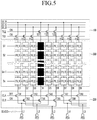
- FIG. 5 illustrates a schematic view of the defect detecting device 100 and the demultiplexer 200 of FIG. 1 in another defective state.
- the second TFTs TB2, TB4, ..., TBm-1 are in the turn-on state, only operations of the pixel array corresponding to the shorted line (e.g., line L1 shorted with the first voltage source ELVDD) are different form the above description of the pixels in a normal state (e.g., not shorted state).
- the line L1 is shorted to the voltage ELVDD.
- a resistor component may exist between the line L1 and the voltage ELVDD.
- the line L1 is connected to the data line D4 through the turned-on second TFT TB4. Accordingly, the data line D4 is supplied with a high level voltage similar to a voltage of the first voltage source ELVDD. Thus, the gate electrode of the respective driving transistor TD is supplied with the high level voltage through the respective switching transistor TS shown in FIG. 2 .
- a plurality of the pixels PX_R connected to the data line D4 emit light with very low luminance. That is, the dark line appears according to the data line D4.
- the line electrically connected to the data line connected to the pixel column that is displayed as a dark line may be detected to be shorted.
- FIG. 6 illustrates a schematic view of the defect detecting device 100 and the demultiplexer 200 of FIG. 1 in another defective state, e.g., a short line is generated. More particularly, FIG. 6 shows a state wherein the line L1 is shorted to the voltage ELVSS. As shown in FIG. 6 , a plurality of the first switches T11-T1a and a plurality of the second switches T21-T2b are all in a turned-on state by the first gate signal TGS1 and the second gate signal TGS2, and a plurality of the second TFTs TB1, TB3, ..., Tbm are in a turned-on state by the second control signal CON2.
- the data lines D4 is supplied with the voltage of the low level similar to the voltage ELVSS. Therefore, the voltage of the low level is supplied to the gate electrode of the driving transistor TD through the switching transistor TS.
- a plurality of pixels PX_R connected to the data line D4 emit light with very high luminance. That is, the bright line appears according to the data lines D4.
- the line electrically connected to the data line connected to the pixel column displayed as the bright line may be detected as shorted.
- the line corresponding to the pixel column that is displayed as the dark line or the bright line among a plurality of pixel columns may be determined as shorted.
- the pixel column connected to the data line D2 is displayed as a bright line (i.e., relatively bright line) or a dark line (i.e., relatively dark line)
- the line L3 is shorted
- the pixel column connected to the data line D6 is displayed as a bright line or a dark line
- the line L5 is shorted
- the pixel column connected to the data line D8 is displayed as the bright line or the dark line.
- FIGS. 7-10 exemplarily show nine (9) pixel columns for understanding and ease of description.
- a plurality of scan lines S1-Sn are transmitted with a plurality of scan signals of the level for turning on the switching transistor TS.
- the level of the red, green, and blue DC voltages RDV, GDV, and BDV may be determined as the appropriate voltage capable of detecting the defective TFT generated in the demultiplexer.
- FIG. 7 illustrates schematic view of the defect detecting device 100 and the demultiplexer 200 of FIG. 1 in another configuration for detecting a defective state within the demultiplexer 200, e.g., a defective TFT is generated in the demultiplexer 200.
- the plurality of second switches T21-T2b are turned on by the second gate signal TG2 and the plurality of first switches T11 - T1a are turned off by the first gate signal TG1.
- thea plurality of first TFTs TA1, TA3, ..., TAm are in the turn-on state by the first control signal CON1
- the plurality of second TFT TB2, TB4, ..., TBm-1 are in the turn-on state by the second control signal CON2.
- the red, green, and blue DC voltages RDV, GDV, and BDV are connected to the plurality of data lines D1-Dm through the plurality of second switches T21-T2b, the plurality of first TFTs TA1, TA3, ..., TAm, and the plurality of second TFTs TB2, TB4, ..., TBm-1 that are turned on.
- all red, green, and blue pixels PX_R, PX_G, and PX_B of the display unit 300 are supplied with the corresponding red, green, and blue DC voltages RDV, GDV, and BDV.
- the red, green, and blue DC voltages RDV, GDV, and BDV for the detection of the defect of the demultiplexer 300 may be determined as a voltage corresponding to a voltage by which no light is emitted from the respective pixels when the demultiplexer works correctly.
- a path including the second switch T21, the data line D4, the second TFT TB4, the first TFT TA1, and the data line D1 is formed, and the red DC voltage RDV is supplied to a plurality of red pixels PX_R connected to the data line D1 and the data line D4.
- a path including the second switch T22, the data line D5, the first TFT TA5, the second TFT TB2, and the data line D2 is formed, and the green DC voltage GDV is supplied to a plurality of green pixels PX_G connected to the data line D2 and the data line D5.
- a path including the second switch T23, the data line D6, the second TFT TB6, the first TFT TA3, and the data line D3 is formed, and the blue DC voltage BDV is supplied to a plurality of blue pixels PX_B connected to the data line D3 and the data line D6.
- the entire display unit 300 displays the black.
- a defective TFT is generated in one or more among the first TFTs TA1, TA3, ..., TAm and the second TFTs TB2, TB4, ..., TBm-1 forming the demultiplexer 200, the data line of the path including the defective TFT is not supplied with the corresponding DC voltage.
- FIG. 8 illustrates a schematic view of the defect detecting device 100 and the demultiplexer 200 of FIG. 1 according to the detecting configuration of Fig. 7 wherein a defective TFT is generated in the demultiplexer 200.
- a defective TFT is generated in the demultiplexer 200.
- the data lines D3 are not supplied with the blue DC voltage BDV. Accordingly, a plurality of pixels PX_B connected to the data line D3 do not display the black and emit light with a predetermined luminance. That is, the bright line is generated.
- the first TFT TA3 instead of the second TFT TB6 is defective, the pixel column connected to the data line D3 is displayed with the bright line. That is, at least one of the first TFT and the second TFT connected to the data line is defective.
- the first TFT TA3 or the second TFT TB6that is defective may be detected by detecting the data line corresponding to the pixels which emit light at a predetermined luminance, i.e. which are brighter than the other pixel lines.
- embodiments are not limited thereto, and a plurality of the first switches T11-T1 a instead of a plurality of the second switches T21-T2b may be turned on.
- FIG. 9 illustrates a schematic view of the defect detecting device 100 and the demultiplexer 200 of FIG. 1 in another configuration for detecting a defective state within the demultiplexer 200, e.g., a defective TFT is generated in the demultiplexer 200.
- the plurality of first TFTs TA1, TA3, ..., TAm are in the turned-on state by the first control signal CON1
- the plurality of second TFT TB2, TB4, ..., TBm-1 are in the turn-on state by the second control signal CON2.
- the red, green, and blue DC voltages RDV, GDV, and BDV are connected to the plurality of data lines D1-Dm through the first switches T11-T 1a, the first TFTs TA1, TA3, ..., TAm, and the second TFTs TB2, TB4, ..., TBm-1 that are turned on.
- all red, green, and blue pixels PX_R, PX_G, and PX_B of the display unit 300 may be supplied with the corresponding red, green, and blue DC voltages RDV, GDV, and BDV, and the red, green, and blue DC voltages RDV, GDV, and BDV to detect the defect of the demultiplexer 300 may be determined as the voltage capable of light-emitting the pixel.
- the path including the first switch T11, the data line D1, the first TFT TA1, the second TFT TB4, and the data line D4 is formed, and the red DC voltage RDV is supplied to a plurality of red pixels PX_R connected to the data line D1 and the data line D4.
- the path including the first switch T12, the data line D2, the second TFT TB2, the first TFT TA5, and the data line D5 is formed, and the green DC voltage GDV is supplied to a plurality of green pixels PX_G connected to the data line D2 and the data line D5.
- the path including the first switch T13, the data line D3, the first TFT TA3, the second TFT TB6, and the data line D6 is formed, and the blue DC voltage BDV is supplied to a plurality of blue pixels PX_B connected to the data line D3 and the data line D6.
- the entire display unit 300 is displayed as black. However, when a defective TFT is generated among the first TFTs TA1, TA3, ..., TAm and the second TFTs TB2, TB4, ..., TBm-1 forming the demultiplexer 200, the data line including the defective TFT is not supplied with the corresponding DC voltage.
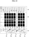
- FIG. 10 illustrates a schematic view of the defect detecting device 100 and the demultiplexer 200 of FIG. 1 according to the detecting configuration of Fig. 9 wherein a defective state within the demultiplexer 200 occurs.
- a defective state within the demultiplexer 200 occurs.
- the data line D6 is not supplied with the blue DC voltage BDV. Accordingly, a plurality of pixels PX_B connected to the data line D6 are not displayed with the black, but are light-emitted with the predetermined luminance. That is, the bright line is generated.
- the first TFT TA3 is defective instead of the second TFT TB6, the pixel column connected to the data line D6 is also displayed with the bright line. That is, at least one of the first TFT and the second TFT connected to the data line is defective.
- the first TFT TA3 or the second TFT TB6 is defective, this may be detected by detecting the bright line that is generated.
Landscapes
- Engineering & Computer Science (AREA)
- Physics & Mathematics (AREA)
- Computer Hardware Design (AREA)
- General Physics & Mathematics (AREA)
- Theoretical Computer Science (AREA)
- Manufacturing & Machinery (AREA)
- Control Of Indicators Other Than Cathode Ray Tubes (AREA)
- Control Of El Displays (AREA)
- Devices For Indicating Variable Information By Combining Individual Elements (AREA)
- Electroluminescent Light Sources (AREA)
- Testing Of Short-Circuits, Discontinuities, Leakage, Or Incorrect Line Connections (AREA)
Applications Claiming Priority (1)
| Application Number | Priority Date | Filing Date | Title |
|---|---|---|---|
| KR1020110127807A KR101943069B1 (ko) | 2011-12-01 | 2011-12-01 | 배선 및 역다중화부의 불량 검출 방법, 불량 검출 장치 및 불량 검출 장치를 포함하는 표시 패널 |
Publications (3)
| Publication Number | Publication Date |
|---|---|
| EP2600627A2 EP2600627A2 (en) | 2013-06-05 |
| EP2600627A3 EP2600627A3 (en) | 2015-07-01 |
| EP2600627B1 true EP2600627B1 (en) | 2018-10-03 |
Family
ID=47018737
Family Applications (1)
| Application Number | Title | Priority Date | Filing Date |
|---|---|---|---|
| EP12179991.0A Active EP2600627B1 (en) | 2011-12-01 | 2012-08-10 | Detecting method of defects of line and demultiplexer, defect detecting device, and display panel including the defect detecting device |
Country Status (6)
| Country | Link |
|---|---|
| US (1) | US9390644B2 (ko) |
| EP (1) | EP2600627B1 (ko) |
| JP (1) | JP6034033B2 (ko) |
| KR (1) | KR101943069B1 (ko) |
| CN (2) | CN103137050B (ko) |
| TW (1) | TWI585425B (ko) |
Families Citing this family (34)
| Publication number | Priority date | Publication date | Assignee | Title |
|---|---|---|---|---|
| KR101943069B1 (ko) * | 2011-12-01 | 2019-04-18 | 삼성디스플레이 주식회사 | 배선 및 역다중화부의 불량 검출 방법, 불량 검출 장치 및 불량 검출 장치를 포함하는 표시 패널 |
| KR102057288B1 (ko) * | 2013-02-21 | 2019-12-19 | 삼성디스플레이 주식회사 | 유기전계발광 표시장치 및 그의 구동방법 |
| KR102098743B1 (ko) | 2013-10-02 | 2020-04-09 | 삼성디스플레이 주식회사 | 유기 발광 표시 패널 |
| TWI502261B (zh) * | 2013-12-12 | 2015-10-01 | Chunghwa Picture Tubes Ltd | 畫素陣列基板及顯示面板 |
| CN104112426B (zh) * | 2014-06-30 | 2016-08-24 | 上海天马有机发光显示技术有限公司 | 一种oled像素驱动电路、静电释放保护电路及检测方法 |
| TWI540323B (zh) | 2014-09-16 | 2016-07-01 | 友達光電股份有限公司 | 顯示面板之測試單元結構與顯示面板 |
| TWI552126B (zh) * | 2014-10-08 | 2016-10-01 | 友達光電股份有限公司 | 亮點偵測方法及顯示面板 |
| CN104392685B (zh) * | 2014-12-15 | 2017-06-09 | 合肥京东方光电科技有限公司 | 阵列基板、显示面板和极性反转驱动方法 |
| KR102295168B1 (ko) * | 2014-12-29 | 2021-08-30 | 삼성디스플레이 주식회사 | 표시 장치 |
| KR102304585B1 (ko) * | 2015-01-30 | 2021-09-27 | 삼성디스플레이 주식회사 | 표시 패널 검사 장치 및 표시 장치 |
| CN104992946B (zh) * | 2015-05-29 | 2018-03-16 | 京东方科技集团股份有限公司 | 一种显示基板及其制备方法、显示面板及显示装置 |
| CN104933979A (zh) | 2015-07-20 | 2015-09-23 | 京东方科技集团股份有限公司 | 检测电路、检测方法和显示装置 |
| US10262590B2 (en) | 2015-08-03 | 2019-04-16 | Sharp Kabushiki Kaisha | Active matrix substrate and display panel |
| KR102462070B1 (ko) * | 2015-12-31 | 2022-11-01 | 엘지디스플레이 주식회사 | 디스플레이패널 및 그 검사 방법 |
| CN105511129B (zh) * | 2016-01-28 | 2019-07-16 | 厦门天马微电子有限公司 | 显示面板、显示装置及显示面板的测试方法 |
| KR102566085B1 (ko) * | 2016-07-07 | 2023-08-14 | 삼성디스플레이 주식회사 | 표시 패널 및 이를 포함하는 표시 장치 |
| CN106057111B (zh) * | 2016-08-09 | 2019-09-13 | 武汉华星光电技术有限公司 | 测试电路及液晶面板 |
| CN106297615B (zh) * | 2016-09-09 | 2017-12-22 | 京东方科技集团股份有限公司 | 显示装置的检测电路及方法 |
| CN106356013B (zh) * | 2016-10-26 | 2019-06-07 | 上海天马微电子有限公司 | 一种阵列基板、检测电路及其断路和短路检测方法 |
| CN106601163A (zh) * | 2016-12-29 | 2017-04-26 | 深圳市华星光电技术有限公司 | 一种液晶盒的辉点检测方法 |
| KR102351323B1 (ko) * | 2017-03-28 | 2022-01-17 | 삼성전자주식회사 | 디스플레이의 균열을 감지하기 위한 회로 및 이를 포함하는 전자 장치 |
| US10453366B2 (en) * | 2017-04-18 | 2019-10-22 | Samsung Display Co., Ltd. | System and method for white spot mura detection |
| JP2018189778A (ja) * | 2017-05-01 | 2018-11-29 | 株式会社ジャパンディスプレイ | 表示装置 |
| CN107728395B (zh) * | 2017-10-31 | 2020-07-03 | 京东方科技集团股份有限公司 | 阵列基板、显示装置、数据线不良的检测装置及检测方法 |
| KR102184669B1 (ko) * | 2018-11-05 | 2020-12-01 | 한국로봇융합연구원 | 신호 배선의 다중화 및 단선감지에 의한 다중 배선 간 전환 제어방법 및 시스템 |
| CN109493769B (zh) * | 2018-11-12 | 2022-03-01 | 成都中电熊猫显示科技有限公司 | 测试方法、装置和存储介质 |
| KR20210055375A (ko) * | 2019-11-07 | 2021-05-17 | 엘지디스플레이 주식회사 | 표시 장치 및 표시 장치의 데이터 링크 라인 결함 검출 방법 |
| CN111063282A (zh) * | 2019-11-27 | 2020-04-24 | 武汉华星光电半导体显示技术有限公司 | 显示面板的测试电路及oled显示器 |
| CN111128063B (zh) * | 2020-01-20 | 2021-03-23 | 云谷(固安)科技有限公司 | 显示面板的测试电路、方法及显示面板 |
| CN111785196A (zh) * | 2020-07-10 | 2020-10-16 | 昆山国显光电有限公司 | 显示面板及其测试方法、显示装置 |
| CN112017543B (zh) * | 2020-08-28 | 2022-11-15 | 昆山国显光电有限公司 | 显示面板及其短路测试方法和显示装置 |
| KR20220147194A (ko) | 2021-04-26 | 2022-11-03 | 삼성디스플레이 주식회사 | 표시 장치 |
| CN113450706B (zh) * | 2021-06-25 | 2023-04-14 | 京东方科技集团股份有限公司 | 检测电路及其驱动方法、显示面板和显示装置 |
| CN114550669A (zh) * | 2022-03-01 | 2022-05-27 | 福建华佳彩有限公司 | 一种补偿Data信号以改善面板残影的驱动方法 |
Family Cites Families (20)
| Publication number | Priority date | Publication date | Assignee | Title |
|---|---|---|---|---|
| US20030085855A1 (en) | 2001-07-17 | 2003-05-08 | Kabushiki Kaisha Toshiba | Array substrate, method of inspecting array substrate, and liquid crystal display |
| JP2003308051A (ja) | 2002-04-16 | 2003-10-31 | Seiko Epson Corp | 画像信号供給回路および電気光学パネル |
| JP4572316B2 (ja) * | 2003-05-30 | 2010-11-04 | セイコーエプソン株式会社 | 電気光学パネルの駆動回路及び方法、電気光学装置並びに電子機器 |
| KR101066495B1 (ko) | 2005-04-07 | 2011-09-21 | 엘지디스플레이 주식회사 | 액정표시장치 및 이의 검사방법 |
| KR101209042B1 (ko) | 2005-11-30 | 2012-12-06 | 삼성디스플레이 주식회사 | 표시 장치 및 그 검사 방법 |
| WO2007069101A1 (en) * | 2005-12-13 | 2007-06-21 | Koninklijke Philips Electronics N.V. | Active matrix array device |
| JP4561647B2 (ja) * | 2006-02-02 | 2010-10-13 | セイコーエプソン株式会社 | 電気光学装置用基板、電気光学装置および検査方法 |
| KR100732819B1 (ko) | 2006-08-30 | 2007-06-27 | 삼성에스디아이 주식회사 | 유기전계발광 표시장치 및 그의 모기판 |
| TW200910600A (en) * | 2007-08-24 | 2009-03-01 | Au Optronics Corp | TFT array substrate |
| JP5428299B2 (ja) | 2008-03-18 | 2014-02-26 | セイコーエプソン株式会社 | 電気光学装置及び電子機器 |
| CN101960509B (zh) * | 2008-07-04 | 2015-04-15 | 松下电器产业株式会社 | 显示装置及其控制方法 |
| JP4780159B2 (ja) * | 2008-08-27 | 2011-09-28 | ソニー株式会社 | 表示装置とその駆動方法 |
| KR20100071536A (ko) | 2008-12-19 | 2010-06-29 | 엘지디스플레이 주식회사 | 표시 패널의 검사장치 및 이를 이용한 검사방법 |
| KR101305379B1 (ko) * | 2009-07-21 | 2013-09-06 | 엘지디스플레이 주식회사 | 씨오지 타입 액정표시장치 및 이의 검사방법 |
| KR101015312B1 (ko) | 2009-08-20 | 2011-02-15 | 삼성모바일디스플레이주식회사 | 유기전계발광 표시장치 및 그의 모기판 |
| CN102043266B (zh) * | 2009-10-21 | 2012-08-01 | 北京京东方光电科技有限公司 | 检测薄膜场效应晶体管阵列基板的设备及方法 |
| EP2528051A4 (en) * | 2010-01-19 | 2013-05-22 | Sharp Kk | DISPLAY PANEL AND INSPECTION METHOD THEREOF |
| JP5445239B2 (ja) * | 2010-03-10 | 2014-03-19 | セイコーエプソン株式会社 | 電気光学装置及び電子機器 |
| US8502842B2 (en) * | 2011-05-24 | 2013-08-06 | Apple Inc. | Offsetting multiple coupling effects in display screens |
| KR101943069B1 (ko) * | 2011-12-01 | 2019-04-18 | 삼성디스플레이 주식회사 | 배선 및 역다중화부의 불량 검출 방법, 불량 검출 장치 및 불량 검출 장치를 포함하는 표시 패널 |
-
2011
- 2011-12-01 KR KR1020110127807A patent/KR101943069B1/ko active IP Right Grant
-
2012
- 2012-03-23 JP JP2012067450A patent/JP6034033B2/ja active Active
- 2012-05-31 US US13/484,644 patent/US9390644B2/en active Active
- 2012-08-10 EP EP12179991.0A patent/EP2600627B1/en active Active
- 2012-10-30 CN CN201210422647.4A patent/CN103137050B/zh active Active
- 2012-10-30 CN CN2012205638782U patent/CN202976770U/zh not_active Expired - Lifetime
- 2012-11-08 TW TW101141623A patent/TWI585425B/zh active
Non-Patent Citations (1)
| Title |
|---|
| None * |
Also Published As
| Publication number | Publication date |
|---|---|
| EP2600627A3 (en) | 2015-07-01 |
| CN202976770U (zh) | 2013-06-05 |
| EP2600627A2 (en) | 2013-06-05 |
| US20130141314A1 (en) | 2013-06-06 |
| US9390644B2 (en) | 2016-07-12 |
| JP6034033B2 (ja) | 2016-11-30 |
| KR101943069B1 (ko) | 2019-04-18 |
| TW201329472A (zh) | 2013-07-16 |
| CN103137050A (zh) | 2013-06-05 |
| KR20130061480A (ko) | 2013-06-11 |
| TWI585425B (zh) | 2017-06-01 |
| CN103137050B (zh) | 2018-01-12 |
| JP2013117709A (ja) | 2013-06-13 |
Similar Documents
| Publication | Publication Date | Title |
|---|---|---|
| EP2600627B1 (en) | Detecting method of defects of line and demultiplexer, defect detecting device, and display panel including the defect detecting device | |
| US10269277B2 (en) | Organic light emitting display panel, organic light emitting display device and the method for driving the same | |
| EP3633660A1 (en) | Pixel driving circuit and repairing method therefor, and display apparatus | |
| US10198977B2 (en) | Display panel | |
| US9990873B2 (en) | Display apparatus and method of testing the same | |
| US11087653B2 (en) | Inspection system and method of inspecting a display cell using the same | |
| WO2017080081A1 (zh) | 采用外部补偿的amoled驱动电路架构 | |
| US11276339B2 (en) | Display device and method of inspecting the same | |
| US9514665B2 (en) | Testing device, and testing method for the line and one sheet using the testing device | |
| US9767732B2 (en) | Display device | |
| US10360845B2 (en) | Display device | |
| EP1575022A2 (en) | Self light emitting display module, electronic equipment into which the same module is loaded, and inspection method of a defect state in the same module | |
| EP1580720A2 (en) | Self light emitting display module, electronic equipment into which the same module is loaded, and inspection method of defect state in the same module | |
| KR20160108639A (ko) | 표시 패널, 표시 장치 및 표시 패널의 구동 방법 | |
| KR102496782B1 (ko) | 전압변환 회로 및 이를 구비한 유기발광 표시장치 | |
| US10354591B2 (en) | Pixel driving circuit, repair method thereof and display device | |
| KR102383751B1 (ko) | 유기발광표시패널, 유기발광표시장치 및 신호 라인 결함 감지 방법 | |
| US8537151B2 (en) | Inspection method | |
| JP2010139833A (ja) | 画像表示装置、画像表示装置の駆動方法及び画像表示装置の製造方法 | |
| KR20210081221A (ko) | 누설 전류를 최소화하는 픽셀 회로 및 디스플레이 장치 및 이의 제어 방법 | |
| JP2005338532A (ja) | アクティブ駆動型発光表示装置および同表示装置を搭載した電子機器 | |
| US7800394B2 (en) | Display device, driving method thereof, and electronic appliance | |
| KR20230089382A (ko) | 전계 발광 표시장치와 그의 표시 결함 검출방법 | |
| KR20220090739A (ko) | 표시 장치 | |
| KR20200025163A (ko) | 유기전계발광표시장치 및 이의 구동방법 |
Legal Events
| Date | Code | Title | Description |
|---|---|---|---|
| PUAI | Public reference made under article 153(3) epc to a published international application that has entered the european phase |
Free format text: ORIGINAL CODE: 0009012 |
|
| AK | Designated contracting states |
Kind code of ref document: A2 Designated state(s): AL AT BE BG CH CY CZ DE DK EE ES FI FR GB GR HR HU IE IS IT LI LT LU LV MC MK MT NL NO PL PT RO RS SE SI SK SM TR |
|
| AX | Request for extension of the european patent |
Extension state: BA ME |
|
| PUAL | Search report despatched |
Free format text: ORIGINAL CODE: 0009013 |
|
| AK | Designated contracting states |
Kind code of ref document: A3 Designated state(s): AL AT BE BG CH CY CZ DE DK EE ES FI FR GB GR HR HU IE IS IT LI LT LU LV MC MK MT NL NO PL PT RO RS SE SI SK SM TR |
|
| AX | Request for extension of the european patent |
Extension state: BA ME |
|
| RIC1 | Information provided on ipc code assigned before grant |
Ipc: G09G 3/00 20060101AFI20150527BHEP Ipc: G09G 3/32 20060101ALI20150527BHEP |
|
| RAP1 | Party data changed (applicant data changed or rights of an application transferred) |
Owner name: SAMSUNG DISPLAY CO., LTD. |
|
| 17P | Request for examination filed |
Effective date: 20151208 |
|
| RBV | Designated contracting states (corrected) |
Designated state(s): AL AT BE BG CH CY CZ DE DK EE ES FI FR GB GR HR HU IE IS IT LI LT LU LV MC MK MT NL NO PL PT RO RS SE SI SK SM TR |
|
| STAA | Information on the status of an ep patent application or granted ep patent |
Free format text: STATUS: EXAMINATION IS IN PROGRESS |
|
| 17Q | First examination report despatched |
Effective date: 20170224 |
|
| REG | Reference to a national code |
Ref country code: DE Ref legal event code: R079 Ref document number: 602012051690 Country of ref document: DE Free format text: PREVIOUS MAIN CLASS: H04N0017000000 Ipc: G09G0003323300 |
|
| GRAP | Despatch of communication of intention to grant a patent |
Free format text: ORIGINAL CODE: EPIDOSNIGR1 |
|
| STAA | Information on the status of an ep patent application or granted ep patent |
Free format text: STATUS: GRANT OF PATENT IS INTENDED |
|
| RIC1 | Information provided on ipc code assigned before grant |
Ipc: G09G 3/3233 20160101AFI20180403BHEP Ipc: G09G 3/3291 20160101ALI20180403BHEP Ipc: G09G 3/00 20060101ALI20180403BHEP |
|
| INTG | Intention to grant announced |
Effective date: 20180418 |
|
| GRAS | Grant fee paid |
Free format text: ORIGINAL CODE: EPIDOSNIGR3 |
|
| GRAA | (expected) grant |
Free format text: ORIGINAL CODE: 0009210 |
|
| STAA | Information on the status of an ep patent application or granted ep patent |
Free format text: STATUS: THE PATENT HAS BEEN GRANTED |
|
| AK | Designated contracting states |
Kind code of ref document: B1 Designated state(s): AL AT BE BG CH CY CZ DE DK EE ES FI FR GB GR HR HU IE IS IT LI LT LU LV MC MK MT NL NO PL PT RO RS SE SI SK SM TR |
|
| REG | Reference to a national code |
Ref country code: GB Ref legal event code: FG4D |
|
| REG | Reference to a national code |
Ref country code: AT Ref legal event code: REF Ref document number: 1049461 Country of ref document: AT Kind code of ref document: T Effective date: 20181015 Ref country code: CH Ref legal event code: EP |
|
| REG | Reference to a national code |
Ref country code: DE Ref legal event code: R096 Ref document number: 602012051690 Country of ref document: DE Ref country code: IE Ref legal event code: FG4D |
|
| REG | Reference to a national code |
Ref country code: NL Ref legal event code: FP |
|
| REG | Reference to a national code |
Ref country code: LT Ref legal event code: MG4D |
|
| REG | Reference to a national code |
Ref country code: AT Ref legal event code: MK05 Ref document number: 1049461 Country of ref document: AT Kind code of ref document: T Effective date: 20181003 |
|
| PG25 | Lapsed in a contracting state [announced via postgrant information from national office to epo] |
Ref country code: NO Free format text: LAPSE BECAUSE OF FAILURE TO SUBMIT A TRANSLATION OF THE DESCRIPTION OR TO PAY THE FEE WITHIN THE PRESCRIBED TIME-LIMIT Effective date: 20190103 Ref country code: IS Free format text: LAPSE BECAUSE OF FAILURE TO SUBMIT A TRANSLATION OF THE DESCRIPTION OR TO PAY THE FEE WITHIN THE PRESCRIBED TIME-LIMIT Effective date: 20190203 Ref country code: CZ Free format text: LAPSE BECAUSE OF FAILURE TO SUBMIT A TRANSLATION OF THE DESCRIPTION OR TO PAY THE FEE WITHIN THE PRESCRIBED TIME-LIMIT Effective date: 20181003 Ref country code: AT Free format text: LAPSE BECAUSE OF FAILURE TO SUBMIT A TRANSLATION OF THE DESCRIPTION OR TO PAY THE FEE WITHIN THE PRESCRIBED TIME-LIMIT Effective date: 20181003 Ref country code: ES Free format text: LAPSE BECAUSE OF FAILURE TO SUBMIT A TRANSLATION OF THE DESCRIPTION OR TO PAY THE FEE WITHIN THE PRESCRIBED TIME-LIMIT Effective date: 20181003 Ref country code: LV Free format text: LAPSE BECAUSE OF FAILURE TO SUBMIT A TRANSLATION OF THE DESCRIPTION OR TO PAY THE FEE WITHIN THE PRESCRIBED TIME-LIMIT Effective date: 20181003 Ref country code: HR Free format text: LAPSE BECAUSE OF FAILURE TO SUBMIT A TRANSLATION OF THE DESCRIPTION OR TO PAY THE FEE WITHIN THE PRESCRIBED TIME-LIMIT Effective date: 20181003 Ref country code: PL Free format text: LAPSE BECAUSE OF FAILURE TO SUBMIT A TRANSLATION OF THE DESCRIPTION OR TO PAY THE FEE WITHIN THE PRESCRIBED TIME-LIMIT Effective date: 20181003 Ref country code: LT Free format text: LAPSE BECAUSE OF FAILURE TO SUBMIT A TRANSLATION OF THE DESCRIPTION OR TO PAY THE FEE WITHIN THE PRESCRIBED TIME-LIMIT Effective date: 20181003 Ref country code: FI Free format text: LAPSE BECAUSE OF FAILURE TO SUBMIT A TRANSLATION OF THE DESCRIPTION OR TO PAY THE FEE WITHIN THE PRESCRIBED TIME-LIMIT Effective date: 20181003 Ref country code: BG Free format text: LAPSE BECAUSE OF FAILURE TO SUBMIT A TRANSLATION OF THE DESCRIPTION OR TO PAY THE FEE WITHIN THE PRESCRIBED TIME-LIMIT Effective date: 20190103 |
|
| PG25 | Lapsed in a contracting state [announced via postgrant information from national office to epo] |
Ref country code: AL Free format text: LAPSE BECAUSE OF FAILURE TO SUBMIT A TRANSLATION OF THE DESCRIPTION OR TO PAY THE FEE WITHIN THE PRESCRIBED TIME-LIMIT Effective date: 20181003 Ref country code: RS Free format text: LAPSE BECAUSE OF FAILURE TO SUBMIT A TRANSLATION OF THE DESCRIPTION OR TO PAY THE FEE WITHIN THE PRESCRIBED TIME-LIMIT Effective date: 20181003 Ref country code: SE Free format text: LAPSE BECAUSE OF FAILURE TO SUBMIT A TRANSLATION OF THE DESCRIPTION OR TO PAY THE FEE WITHIN THE PRESCRIBED TIME-LIMIT Effective date: 20181003 Ref country code: GR Free format text: LAPSE BECAUSE OF FAILURE TO SUBMIT A TRANSLATION OF THE DESCRIPTION OR TO PAY THE FEE WITHIN THE PRESCRIBED TIME-LIMIT Effective date: 20190104 Ref country code: PT Free format text: LAPSE BECAUSE OF FAILURE TO SUBMIT A TRANSLATION OF THE DESCRIPTION OR TO PAY THE FEE WITHIN THE PRESCRIBED TIME-LIMIT Effective date: 20190203 |
|
| REG | Reference to a national code |
Ref country code: DE Ref legal event code: R097 Ref document number: 602012051690 Country of ref document: DE |
|
| PG25 | Lapsed in a contracting state [announced via postgrant information from national office to epo] |
Ref country code: DK Free format text: LAPSE BECAUSE OF FAILURE TO SUBMIT A TRANSLATION OF THE DESCRIPTION OR TO PAY THE FEE WITHIN THE PRESCRIBED TIME-LIMIT Effective date: 20181003 Ref country code: IT Free format text: LAPSE BECAUSE OF FAILURE TO SUBMIT A TRANSLATION OF THE DESCRIPTION OR TO PAY THE FEE WITHIN THE PRESCRIBED TIME-LIMIT Effective date: 20181003 |
|
| PLBE | No opposition filed within time limit |
Free format text: ORIGINAL CODE: 0009261 |
|
| STAA | Information on the status of an ep patent application or granted ep patent |
Free format text: STATUS: NO OPPOSITION FILED WITHIN TIME LIMIT |
|
| PG25 | Lapsed in a contracting state [announced via postgrant information from national office to epo] |
Ref country code: RO Free format text: LAPSE BECAUSE OF FAILURE TO SUBMIT A TRANSLATION OF THE DESCRIPTION OR TO PAY THE FEE WITHIN THE PRESCRIBED TIME-LIMIT Effective date: 20181003 Ref country code: EE Free format text: LAPSE BECAUSE OF FAILURE TO SUBMIT A TRANSLATION OF THE DESCRIPTION OR TO PAY THE FEE WITHIN THE PRESCRIBED TIME-LIMIT Effective date: 20181003 Ref country code: SM Free format text: LAPSE BECAUSE OF FAILURE TO SUBMIT A TRANSLATION OF THE DESCRIPTION OR TO PAY THE FEE WITHIN THE PRESCRIBED TIME-LIMIT Effective date: 20181003 Ref country code: SK Free format text: LAPSE BECAUSE OF FAILURE TO SUBMIT A TRANSLATION OF THE DESCRIPTION OR TO PAY THE FEE WITHIN THE PRESCRIBED TIME-LIMIT Effective date: 20181003 |
|
| 26N | No opposition filed |
Effective date: 20190704 |
|
| PG25 | Lapsed in a contracting state [announced via postgrant information from national office to epo] |
Ref country code: SI Free format text: LAPSE BECAUSE OF FAILURE TO SUBMIT A TRANSLATION OF THE DESCRIPTION OR TO PAY THE FEE WITHIN THE PRESCRIBED TIME-LIMIT Effective date: 20181003 |
|
| PG25 | Lapsed in a contracting state [announced via postgrant information from national office to epo] |
Ref country code: TR Free format text: LAPSE BECAUSE OF FAILURE TO SUBMIT A TRANSLATION OF THE DESCRIPTION OR TO PAY THE FEE WITHIN THE PRESCRIBED TIME-LIMIT Effective date: 20181003 |
|
| PG25 | Lapsed in a contracting state [announced via postgrant information from national office to epo] |
Ref country code: MC Free format text: LAPSE BECAUSE OF FAILURE TO SUBMIT A TRANSLATION OF THE DESCRIPTION OR TO PAY THE FEE WITHIN THE PRESCRIBED TIME-LIMIT Effective date: 20181003 Ref country code: LU Free format text: LAPSE BECAUSE OF NON-PAYMENT OF DUE FEES Effective date: 20190810 Ref country code: LI Free format text: LAPSE BECAUSE OF NON-PAYMENT OF DUE FEES Effective date: 20190831 Ref country code: CH Free format text: LAPSE BECAUSE OF NON-PAYMENT OF DUE FEES Effective date: 20190831 |
|
| REG | Reference to a national code |
Ref country code: BE Ref legal event code: MM Effective date: 20190831 |
|
| PG25 | Lapsed in a contracting state [announced via postgrant information from national office to epo] |
Ref country code: IE Free format text: LAPSE BECAUSE OF NON-PAYMENT OF DUE FEES Effective date: 20190810 |
|
| PG25 | Lapsed in a contracting state [announced via postgrant information from national office to epo] |
Ref country code: BE Free format text: LAPSE BECAUSE OF NON-PAYMENT OF DUE FEES Effective date: 20190831 |
|
| PG25 | Lapsed in a contracting state [announced via postgrant information from national office to epo] |
Ref country code: CY Free format text: LAPSE BECAUSE OF FAILURE TO SUBMIT A TRANSLATION OF THE DESCRIPTION OR TO PAY THE FEE WITHIN THE PRESCRIBED TIME-LIMIT Effective date: 20181003 |
|
| PG25 | Lapsed in a contracting state [announced via postgrant information from national office to epo] |
Ref country code: MT Free format text: LAPSE BECAUSE OF FAILURE TO SUBMIT A TRANSLATION OF THE DESCRIPTION OR TO PAY THE FEE WITHIN THE PRESCRIBED TIME-LIMIT Effective date: 20181003 Ref country code: HU Free format text: LAPSE BECAUSE OF FAILURE TO SUBMIT A TRANSLATION OF THE DESCRIPTION OR TO PAY THE FEE WITHIN THE PRESCRIBED TIME-LIMIT; INVALID AB INITIO Effective date: 20120810 |
|
| PG25 | Lapsed in a contracting state [announced via postgrant information from national office to epo] |
Ref country code: MK Free format text: LAPSE BECAUSE OF FAILURE TO SUBMIT A TRANSLATION OF THE DESCRIPTION OR TO PAY THE FEE WITHIN THE PRESCRIBED TIME-LIMIT Effective date: 20181003 |
|
| P01 | Opt-out of the competence of the unified patent court (upc) registered |
Effective date: 20230515 |
|
| PGFP | Annual fee paid to national office [announced via postgrant information from national office to epo] |
Ref country code: NL Payment date: 20230721 Year of fee payment: 12 |
|
| PGFP | Annual fee paid to national office [announced via postgrant information from national office to epo] |
Ref country code: GB Payment date: 20230720 Year of fee payment: 12 |
|
| PGFP | Annual fee paid to national office [announced via postgrant information from national office to epo] |
Ref country code: FR Payment date: 20230725 Year of fee payment: 12 Ref country code: DE Payment date: 20230720 Year of fee payment: 12 |