EP2600145A1 - Leitkleberverbindung - Google Patents
Leitkleberverbindung Download PDFInfo
- Publication number
- EP2600145A1 EP2600145A1 EP20120007745 EP12007745A EP2600145A1 EP 2600145 A1 EP2600145 A1 EP 2600145A1 EP 20120007745 EP20120007745 EP 20120007745 EP 12007745 A EP12007745 A EP 12007745A EP 2600145 A1 EP2600145 A1 EP 2600145A1
- Authority
- EP
- European Patent Office
- Prior art keywords
- fastening device
- layer
- component
- connecting means
- passivation layer
- Prior art date
- Legal status (The legal status is an assumption and is not a legal conclusion. Google has not performed a legal analysis and makes no representation as to the accuracy of the status listed.)
- Granted
Links
Images
Classifications
-
- H—ELECTRICITY
- H10—SEMICONDUCTOR DEVICES; ELECTRIC SOLID-STATE DEVICES NOT OTHERWISE PROVIDED FOR
- H10W—GENERIC PACKAGES, INTERCONNECTIONS, CONNECTORS OR OTHER CONSTRUCTIONAL DETAILS OF DEVICES COVERED BY CLASS H10
- H10W72/00—Interconnections or connectors in packages
-
- G—PHYSICS
- G01—MEASURING; TESTING
- G01N—INVESTIGATING OR ANALYSING MATERIALS BY DETERMINING THEIR CHEMICAL OR PHYSICAL PROPERTIES
- G01N27/00—Investigating or analysing materials by the use of electric, electrochemical, or magnetic means
- G01N27/26—Investigating or analysing materials by the use of electric, electrochemical, or magnetic means by investigating electrochemical variables; by using electrolysis or electrophoresis
- G01N27/403—Cells and electrode assemblies
- G01N27/414—Ion-sensitive or chemical field-effect transistors, i.e. ISFETS or CHEMFETS
- G01N27/4148—Integrated circuits therefor, e.g. fabricated by CMOS processing
-
- H—ELECTRICITY
- H10—SEMICONDUCTOR DEVICES; ELECTRIC SOLID-STATE DEVICES NOT OTHERWISE PROVIDED FOR
- H10W—GENERIC PACKAGES, INTERCONNECTIONS, CONNECTORS OR OTHER CONSTRUCTIONAL DETAILS OF DEVICES COVERED BY CLASS H10
- H10W20/00—Interconnections in chips, wafers or substrates
- H10W20/40—Interconnections external to wafers or substrates, e.g. back-end-of-line [BEOL] metallisations or vias connecting to gate electrodes
-
- H—ELECTRICITY
- H10—SEMICONDUCTOR DEVICES; ELECTRIC SOLID-STATE DEVICES NOT OTHERWISE PROVIDED FOR
- H10W—GENERIC PACKAGES, INTERCONNECTIONS, CONNECTORS OR OTHER CONSTRUCTIONAL DETAILS OF DEVICES COVERED BY CLASS H10
- H10W72/00—Interconnections or connectors in packages
- H10W72/30—Die-attach connectors
-
- H—ELECTRICITY
- H10—SEMICONDUCTOR DEVICES; ELECTRIC SOLID-STATE DEVICES NOT OTHERWISE PROVIDED FOR
- H10W—GENERIC PACKAGES, INTERCONNECTIONS, CONNECTORS OR OTHER CONSTRUCTIONAL DETAILS OF DEVICES COVERED BY CLASS H10
- H10W74/00—Encapsulations, e.g. protective coatings
- H10W74/01—Manufacture or treatment
- H10W74/012—Manufacture or treatment of encapsulations on active surfaces of flip-chip devices, e.g. forming underfills
-
- H—ELECTRICITY
- H10—SEMICONDUCTOR DEVICES; ELECTRIC SOLID-STATE DEVICES NOT OTHERWISE PROVIDED FOR
- H10W—GENERIC PACKAGES, INTERCONNECTIONS, CONNECTORS OR OTHER CONSTRUCTIONAL DETAILS OF DEVICES COVERED BY CLASS H10
- H10W74/00—Encapsulations, e.g. protective coatings
- H10W74/10—Encapsulations, e.g. protective coatings characterised by their shape or disposition
- H10W74/131—Encapsulations, e.g. protective coatings characterised by their shape or disposition the semiconductor body being only partially enclosed
- H10W74/137—Encapsulations, e.g. protective coatings characterised by their shape or disposition the semiconductor body being only partially enclosed the encapsulations being directly on the semiconductor body
-
- H—ELECTRICITY
- H10—SEMICONDUCTOR DEVICES; ELECTRIC SOLID-STATE DEVICES NOT OTHERWISE PROVIDED FOR
- H10W—GENERIC PACKAGES, INTERCONNECTIONS, CONNECTORS OR OTHER CONSTRUCTIONAL DETAILS OF DEVICES COVERED BY CLASS H10
- H10W74/00—Encapsulations, e.g. protective coatings
- H10W74/10—Encapsulations, e.g. protective coatings characterised by their shape or disposition
- H10W74/15—Encapsulations, e.g. protective coatings characterised by their shape or disposition on active surfaces of flip-chip devices, e.g. underfills
-
- H—ELECTRICITY
- H05—ELECTRIC TECHNIQUES NOT OTHERWISE PROVIDED FOR
- H05K—PRINTED CIRCUITS; CASINGS OR CONSTRUCTIONAL DETAILS OF ELECTRIC APPARATUS; MANUFACTURE OF ASSEMBLAGES OF ELECTRICAL COMPONENTS
- H05K2201/00—Indexing scheme relating to printed circuits covered by H05K1/00
- H05K2201/03—Conductive materials
- H05K2201/0332—Structure of the conductor
- H05K2201/0364—Conductor shape
- H05K2201/0373—Conductors having a fine structure, e.g. providing a plurality of contact points with a structured tool
-
- H—ELECTRICITY
- H05—ELECTRIC TECHNIQUES NOT OTHERWISE PROVIDED FOR
- H05K—PRINTED CIRCUITS; CASINGS OR CONSTRUCTIONAL DETAILS OF ELECTRIC APPARATUS; MANUFACTURE OF ASSEMBLAGES OF ELECTRICAL COMPONENTS
- H05K3/00—Apparatus or processes for manufacturing printed circuits
- H05K3/40—Forming printed elements for providing electric connections to or between printed circuits
- H05K3/4007—Surface contacts, e.g. bumps
-
- H—ELECTRICITY
- H10—SEMICONDUCTOR DEVICES; ELECTRIC SOLID-STATE DEVICES NOT OTHERWISE PROVIDED FOR
- H10W—GENERIC PACKAGES, INTERCONNECTIONS, CONNECTORS OR OTHER CONSTRUCTIONAL DETAILS OF DEVICES COVERED BY CLASS H10
- H10W72/00—Interconnections or connectors in packages
- H10W72/071—Connecting or disconnecting
- H10W72/073—Connecting or disconnecting of die-attach connectors
- H10W72/07321—Aligning
- H10W72/07327—Aligning involving guiding structures, e.g. spacers or supporting members
-
- H—ELECTRICITY
- H10—SEMICONDUCTOR DEVICES; ELECTRIC SOLID-STATE DEVICES NOT OTHERWISE PROVIDED FOR
- H10W—GENERIC PACKAGES, INTERCONNECTIONS, CONNECTORS OR OTHER CONSTRUCTIONAL DETAILS OF DEVICES COVERED BY CLASS H10
- H10W72/00—Interconnections or connectors in packages
- H10W72/30—Die-attach connectors
- H10W72/321—Structures or relative sizes of die-attach connectors
- H10W72/325—Die-attach connectors having a filler embedded in a matrix
-
- H—ELECTRICITY
- H10—SEMICONDUCTOR DEVICES; ELECTRIC SOLID-STATE DEVICES NOT OTHERWISE PROVIDED FOR
- H10W—GENERIC PACKAGES, INTERCONNECTIONS, CONNECTORS OR OTHER CONSTRUCTIONAL DETAILS OF DEVICES COVERED BY CLASS H10
- H10W72/00—Interconnections or connectors in packages
- H10W72/30—Die-attach connectors
- H10W72/351—Materials of die-attach connectors
- H10W72/353—Materials of die-attach connectors not comprising solid metals or solid metalloids, e.g. ceramics
- H10W72/354—Materials of die-attach connectors not comprising solid metals or solid metalloids, e.g. ceramics comprising polymers
-
- H—ELECTRICITY
- H10—SEMICONDUCTOR DEVICES; ELECTRIC SOLID-STATE DEVICES NOT OTHERWISE PROVIDED FOR
- H10W—GENERIC PACKAGES, INTERCONNECTIONS, CONNECTORS OR OTHER CONSTRUCTIONAL DETAILS OF DEVICES COVERED BY CLASS H10
- H10W72/00—Interconnections or connectors in packages
- H10W72/50—Bond wires
- H10W72/59—Bond pads specially adapted therefor
-
- H—ELECTRICITY
- H10—SEMICONDUCTOR DEVICES; ELECTRIC SOLID-STATE DEVICES NOT OTHERWISE PROVIDED FOR
- H10W—GENERIC PACKAGES, INTERCONNECTIONS, CONNECTORS OR OTHER CONSTRUCTIONAL DETAILS OF DEVICES COVERED BY CLASS H10
- H10W72/00—Interconnections or connectors in packages
- H10W72/90—Bond pads, in general
- H10W72/931—Shapes of bond pads
-
- H—ELECTRICITY
- H10—SEMICONDUCTOR DEVICES; ELECTRIC SOLID-STATE DEVICES NOT OTHERWISE PROVIDED FOR
- H10W—GENERIC PACKAGES, INTERCONNECTIONS, CONNECTORS OR OTHER CONSTRUCTIONAL DETAILS OF DEVICES COVERED BY CLASS H10
- H10W72/00—Interconnections or connectors in packages
- H10W72/90—Bond pads, in general
- H10W72/951—Materials of bond pads
- H10W72/952—Materials of bond pads comprising metals or metalloids, e.g. PbSn, Ag or Cu
-
- H—ELECTRICITY
- H10—SEMICONDUCTOR DEVICES; ELECTRIC SOLID-STATE DEVICES NOT OTHERWISE PROVIDED FOR
- H10W—GENERIC PACKAGES, INTERCONNECTIONS, CONNECTORS OR OTHER CONSTRUCTIONAL DETAILS OF DEVICES COVERED BY CLASS H10
- H10W74/00—Encapsulations, e.g. protective coatings
- H10W74/10—Encapsulations, e.g. protective coatings characterised by their shape or disposition
- H10W74/131—Encapsulations, e.g. protective coatings characterised by their shape or disposition the semiconductor body being only partially enclosed
Definitions
- the invention relates to a fastening device according to the preamble of patent claim 1.
- the object of the invention is to provide a fastening device which further develops the prior art.
- a fastening device comprising a semiconductor body with an integrated circuit, a dielectric passivation layer formed on the surface of the semiconductor body, a transistor formed below the passivation layer A conductor track and an oxide layer formed below the track, and a connecting means comprising an organic polymer, which forms a frictional connection between a component formed above the passivation layer and the semiconductor body, wherein a passivation layer and the oxide layer penetrating formation is formed with a bottom surface and formed on the bottom surface and / or on a side surface of the molding a conductive layer and the connecting means comprises an organic polymer and forms an electrical connection between the conductive layer and the component.
- bonding agent refers to bonding agents which are liquid at room temperature.
- Such connecting means are also referred to as conductive adhesive.
- the term "separate” includes in particular those components which are not produced in the manufacturing process of the integrated circuit. Investigations have shown that with the novel attachment a complex mechanical attachment preferably by means of a lever or latching mechanism or other fastening means and an additional separate electrical connection, for example by means of a bonding wire deleted.
- the new technology enables simple, reliable and cost-effective connections between a semiconductor body and separate components.
- components is understood in particular as meaning electronic, electromechanical components and parts thereof, such as a separate control electrode of a gas sensor transistor.
- the component is provided as a first part and the connecting means as a second part of an integrated component formed below the passivation layer.
- the connecting means is a second part of an integrated component formed below the passivation layer.
- the individual parts of the integrated component are in an electrically operative connection and only together form the complete component.
- the passivation layer forms a plateau.
- the component is lying on the plateau.
- the connecting means outside the molding on the passivation layer forms a large contact area, wherein the first component rests on the support area.
- a large contact area is understood to mean an area whose dimensions are substantially greater than the area of the formation in the plane of the passivation layer.
- Another advantage is that the production of the molding is already carried out at the so-called wafer level level and thereby the production of the molding can be easily incorporated into the manufacturing process of an integrated circuit.
- a dry etching process in particular the pad window etching process after the application of the passivation, is used to produce the molding.
- Such manufacturing steps after application are also referred to as back end of line processes.
- the connecting means is preferably designed as a conductive adhesive.
- the elevations are designed to be conductive.
- the connecting means forms a particularly reliable mechanical and / or electrical connection with the molding and in particular with the bottom surface.
- the tungsten plugs and the elevations increase the surface and thereby the surface to be wetted with the bonding agent.
- the conductive layer contains silicon.
- the conductive layer is formed by a metallic trace or a metal trace.
- the connecting means fills the molding completely. This makes it possible to form particularly reliable connections between the semiconductor body and the component.
- One advantage is that the bonding agent seals the molding against contamination so that no foreign matter penetrates.
- the shape trench-shaped or hole-shaped it is preferable to design the shape trench-shaped or hole-shaped.
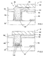
- FIG. 1 10 shows a cross-sectional view of a first embodiment of a fastening device 10, comprising a semiconductor body 20, an integrated circuit-not shown-a conductive polysilicon layer 30 formed on the surface of the semiconductor body 20, an oxide layer 40, a conductor track 45 resting on the oxide layer 40, and a passivation 50.
- the conductor track 45 is part of an uppermost conductor track, not shown, which also forms the metal surfaces for receiving bonding wires.
- the oxide layer 40 preferably consists of a plurality of oxide layers, wherein the oxide layers are generally deposited in the context of the formation of a multi-level metallization.
- the passivation 50 is preferably made of silicon nitride and forms a plateau 55 above the conductor 45. On the plateau 55 resting on a to be connected to the semiconductor body 20 component 60, which is formed for example as a control electrode of a gas sensor, is arranged.
- the form-fitting resting member 60 forms with the plateau 55 a fold.
- the connecting means 80 completely fills the molding 70 and the fold. Furthermore, part of the side surface of the component 60 and part of the passivation 50 on the surface of the semiconductor body 20 are also encompassed by the connection means 80. As a result, the connecting means 80 forms both an electrical contact and a frictional connection between the semiconductor body 20 and the component 60.
- the compound is also very reliable and resistant to aging.
- An advantage of the complete filling of the formation 70 is the passivating construction produced thereby, ie the penetration of foreign substances is suppressed.
- the component 60 is preferably designed to be electrically conductive at least on the side facing the passivation 50.
- a formation 70 is preferably formed as a trench or hole-like structure and passes through the passivation 50, wherein in the bottom region of the molding 70, the polysilicon layer 30 and on the walls of the molding 70, the passivation 50 is formed.
- the formation 70 has been applied by means of an etching process prior to the deposition of the passivation 50.
- the polysilicon layer 30 is exposed by a so-called pad window etching process in the bottom area of the molding 70.
- the formation 70 can also be produced after the passivation 50 has been deposited.
- no passivation layer 50 is formed on the side surfaces of the molding 70.
- connection means 80 partially surrounds the component 60 on a side surface and forms a material connection with the component 60 and with the surface of the molding.
- the component 60 completely covers the molding 70. Between the component 60 and the passivation 50, the connecting means 80 is formed outside the molding 70, ie, a large contact area for the component 70 is formed.
- On the bottom surface of the molding 70 or on the polysilicon layer 30 is a plurality of frusto-conical elevations, which are preferably formed as tungsten plugs 100, respectively.
- the tungsten plugs 100 form with the pad, which preferably has a silicide layer (not shown), most preferably a tungsten silicide layer, a cohesive and non-positive connection.
- the tungsten plugs 100 are each covered with the connecting means 80. As a result, a particularly firm and reliable connection between the connecting means 80 and the bottom region of the molding 70 is achieved.
Landscapes
- Chemical & Material Sciences (AREA)
- Engineering & Computer Science (AREA)
- Microelectronics & Electronic Packaging (AREA)
- Health & Medical Sciences (AREA)
- Life Sciences & Earth Sciences (AREA)
- Electrochemistry (AREA)
- General Health & Medical Sciences (AREA)
- Chemical Kinetics & Catalysis (AREA)
- Computer Hardware Design (AREA)
- Physics & Mathematics (AREA)
- Analytical Chemistry (AREA)
- Biochemistry (AREA)
- Molecular Biology (AREA)
- General Physics & Mathematics (AREA)
- Immunology (AREA)
- Pathology (AREA)
- Internal Circuitry In Semiconductor Integrated Circuit Devices (AREA)
- Investigating Or Analyzing Materials By The Use Of Electric Means (AREA)
- Semiconductor Integrated Circuits (AREA)
Abstract
Description
- Die Erfindung betrifft eine Befestigungsvorrichtung gemäß dem Oberbegriff des Patentanspruchs 1.
- Aus der
DE 10 2005 009 163 A1 ist bekannt, dass auf der passivierten Oberfläche eines Halbleiterkörpers Elektroden mittels Leitklebers zum Anschluss von Bauteilen ausgebildet werden. Des Weiteren ist aus derDE 10 2006 053 461 A1 eine Vorrichtung und Verfahren zum Herstellen einer mikroelektronischen Baugruppe bekannt. - Aus der
DE 100 36 178 A1 , derDE 42 39 319 C2 und derEP 1 103 808 B1 sind FET-Feuchtesensoren bekannt, bei denen die durch einen Luftspalt von dem Kanalbereich beanstandete Steuerelektrode mittels eines Bondverfahrens mit dem Halbleiterkörper elektrisch verschaltet ist. Die Steuerelektrode wird zusätzlich mittels einer Klemmvorrichtung mit dem Halbleiterkörper kraftschlüssig verbunden. - Des Weiteren sind aus der
DE 199 07 168 C1 , derUS 5 545 589 A , derUS 5137 461 A und derUS 5432 675 A weitere Befestigungsvorrichtungen bekannt. - Vor diesem Hintergrund besteht die Aufgabe der Erfindung darin, eine Befestigungsvorrichtung anzugeben, der den Stand der Technik weiterbildet.
- Die Aufgabe wird durch eine Befestigungsvorrichtung mit den Merkmalen des Patentanspruchs 1 gelöst. Vorteilhafte Ausgestaltungen der Erfindung sind in den Unteransprüchen enthalten.
- Gemäß dem Gegenstand der Erfindung wird Befestigungsvorrichtung bereitgestellt, aufweisend einen Halbleiterkörper mit einer integrierten Schaltung, einer an der Oberfläche des Halbleiterkörpers ausgebildeten dielektrischen Passivierungsschicht, eine unterhalb der Passivierungsschicht ausgebildete Leiterbahn und einer unterhalb der Leiterbahn ausgebildeten Oxidschicht, und einem Verbindungsmittel, das ein organisches Polymer umfasst, das eine kraftschlüssige Verbindung zwischen einem oberhalb der Passivierungsschicht ausgebildeten Bauteil und dem Halbleiterkörper ausbildet, wobei eine die Passivierungsschicht und die Oxidschicht durchdringende Ausformung mit einer Bodenfläche ausgebildet ist und an der Bodenfläche und / oder an einer Seitenfläche der Ausformung eine leitfähige Schicht ausgebildet ist und das Verbindungsmittel ein organisches Polymer umfasst und eine elektrische Verbindung zwischen der leitfähigen Schicht und dem Bauteil ausbildet. Es sei angemerkt, dass unter dem Begriff des Verbindungsmittels, derartige Verbindungsmittel verstanden werden, welche bei Raumtemperatur flüssig sind. Derartige Verbindungsmittel werden auch als Leitkleber bezeichnet.
- Ein Vorteil ist, dass sich mittels eines elektrisch leitfähigen Verbindungsmittels weitere Teile von separaten Bauteilen mit dem Halbleiterkörper sowohl elektrisch als auch gleichzeitig kraftschlüssig verbinden lassen. Hierbei werden mit dem Ausdruck "separat" insbesondere solche Bauteile umfasst, welche nicht in dem Herstellungsprozess der integrierten Schaltung erzeugt werden. Untersuchungen haben gezeigt, dass mit der neuartigen Befestigung eine aufwändige mechanische Anbringung vorzugsweise mittels eines Hebel- oder Einrastmechanismus oder anderen Befestigungsmitteln und einer zusätzlich separaten elektrischen Verbindung beispielsweise mittels eines Bonddrahtes entfällt. Mit der neuen Technik lassen sich einfache, zuverlässige und kostengünstige Verbindungen zwischen einem Halbleiterkörper und separaten Bauteilen schaffen. Unter dem Begriff Bauteile werden insbesondere elektronische, elektromechanische Bauteile und Teile davon wie beispielsweise eine separate Steuerelektrode eines Gassensortransistors verstanden. Hierbei ist das Bauteil als ein erster Teil und das Verbindungsmittel als ein zweiter Teil eines unterhalb der Passivierungsschicht ausgebildeten integrierten Bauelements vorgesehen. Vorzugsweise besteht zwischen den unterschiedlichen Teilen eine Signalverbindung. Anders ausgedrückt stehen die einzelnen Teile des integrierten Bauelements in einer elektrischen Wirkverbindung und bilden erst gemeinsam das vollständige Bauelement aus. In einer bevorzugten Ausführungsform bildet die Passivierungsschicht ein Plateau aus. Das Bauteil liegt auf dem Plateau auf. In einer alternativen Ausführungsform bildet das Verbindungsmittel außerhalb der Ausformung auf der Passivierungsschicht einen großen Auflagebereich aus, wobei das erste Bauteil auf dem Auflagebereich aufliegt. Unter einem großen Auflagebereich wird eine Fläche verstanden, deren Maße wesentlich größer als die Fläche der Ausformung in der Ebene der Passivierungsschicht ist.
- Ein weiterer Vorteil ist, dass die Herstellung der Ausformung bereits auf der sogenannten Waferlevelebene durchgeführt wird und hierdurch sich die Herstellung der Ausformung ohne Weiters in den Herstellungsprozess einer integrierten Schaltung einfügen lässt. Vorzugsweise wird zur Herstellung der Ausformung ein Trockenätzprozess, insbesondere der Padfensterätzprozess nach dem Aufbringung der Passivierung verwendet. Derartige Herstellungsschritte nach dem Aufbringen werden auch als Back End of Line Prozesse bezeichnet.
- Weitere Untersuchungen haben gezeigt, dass je nach Verwendung bereits eine geringe elektrische Leitfähigkeit des Verbindungsmittels unterhalb 50 MOhm, höchst vorzugsweise unterhalb 1 MOhm ausreicht, um eine beispielsweise eine separate Steuerelektrode eines SGFETs oder CCFETs mit der Unterlage, d.h. dem Halbleiterköper zu verbinden. Hierdurch lässt sich die Herstellung der Gassensoren kostengünstiger und zuverlässiger ausführen. Des Weiteren verringert sich die Bauhöhe gegenüber einer Ausführung mit einem Bonddraht auf der Deckfläche der Steuerelektrode.
- Gemäß einer bevorzugten Ausführungsform ist auf der Bodenfläche eine, vorzugsweise eine Vielzahl von Erhöhungen, die insbesondere kegelstumpfartig ausgeformt sind, ausgebildet. Bevorzugt ist, dass die Erhöhung von dem Verbindungsmittel vollständig umschlossen ist und insbesondere die Erhöhung mit dem Verbindungsmittel eine stoffschlüssige Verbindung ausbildet. Hierbei ist das Verbindungsmittel vorzugsweise als Leitkleber ausgebildet.
- Gemäß einer Weiterbildung sind die Erhöhungen leitfähig ausgebildet, Insbesondere ist es bevorzugt, die Erhöhungen als Wolframplugs auszubilden. Ein Vorteil der Erhöhungen ist es, dass das Verbindungsmittel eine besonders zuverlässige mechanische und / oder elektrische Verbindung mit der Ausformung und insbesondere mit der Bodenfläche ausbildet. Anders ausgedrückt vergrößern die Wolframplugs bzw. die Erhöhungen die Oberfläche und hierdurch die mit dem Verbindungsmittel zu benetzende Oberfläche.
- Gemäß einer anderen Ausführungsform enthält die leitfähige Schicht Silizium. Bevorzugt hierbei ist, dass die leitfähige Schicht eine dotierte Polysiliziumschicht und / oder einer Silizidschicht umfasst. In einer alternativen Ausführungsform wird die leitfähige Schicht von einer metallischen Leiterbahn oder einer Metallbahn gebildet.
- In einer Weiterbildung füllt das Verbindungsmittel die Ausformung vollständig aus. Hierdurch lassen sich besonders zuverlässige Verbindungen zwischen dem Halbleiterkörper und dem Bauteil ausbilden. Ein Vorteil ist, dass das Verbindungsmittel die Ausformung gegen Verunreinigungen abdichtet, so dass keine Fremdstoffe eindringen.
- Gemäß einer Weiterbildung ist es bevorzugt, die Ausformung grabenförmig oder lochförmig auszubilden. Gemäß einer alternativen Ausführungsform ist es bevorzugt, ein Teil einer Seitenfläche der Ausformung mit einer leitfähigen Schicht auszubilden. Untersuchungen haben gezeigt, dass sich innerhalb der Ausformung sowohl eine Leiterbahnschicht als auch eine siliziumhaltige Schicht, vorzugsweise eine dotierte Polysiliziumschicht mit einer aufliegenden Silizidschicht eignet. Hierbei ist es vorteilhaft, die Silizidschicht als Wolframsilizid auszubilden.
- Die Erfindung wird nachfolgend unter Bezugnahme auf die Zeichnungen näher erläutert. Hierbei werden gleichartige Teile mit identischen Bezeichnungen beschriftet. Die dargestellte Ausführungsformen sind stark schematisiert, d.h. die Abstände und laterale und vertikale Erstreckung sind nicht maßstäblich und weisen, sofern nicht anders angegeben auch keine ableitbare geometrische Relation zueinander auf. Darin zeigen die:
- Figur 1
- eine Querschnittsansicht auf eine erste Ausführungsform,
- Figur 2
- eine Querschnittsansicht auf eine zweite Ausführungsform.
- Die Abbildung der
Figur 1 zeigt eine Querschnittsansicht auf eine erste Ausführungsform einer Befestigungsvorrichtung 10, aufweisend einen Halbleiterkörper 20, eine integrierte Schaltung - nicht dargestellt- eine auf der Oberfläche des Halbleiterkörpers 20 ausgebildete leitfähige Polysiliziumschicht 30, eine Oxidschicht 40, eine auf der Oxidschicht 40 aufliegende Leiterbahn 45 und eine Passivierung 50. Es sei angemerkt, dass die Leiterbahn 45 Teil einer nicht weiter dargestellten obersten Leiterbahnebene, die auch die Metallflächen zur Aufnahme von Bonddrähten ausbildet, ist. Ferner besteht die Oxidschicht 40 vorzugsweise aus mehreren Oxidschichten, wobei die Oxidschichten im Allgemeinen im Rahmen der Ausbildung einer Mehrebenenmetallisierung abgeschieden werden. Die Passivierung 50 besteht vorzugsweise aus Siliziumnitrid und bildet oberhalb der Leiterbahn 45 ein Plateau 55 aus. Auf dem Plateau 55 aufliegend ist ein mit dem Halbleiterkörper 20 anzuschließendes Bauteil 60, das beispielsweise als Steuerelektrode eines Gassensors ausgebildet ist, angeordnet. Das formschlüssig aufliegende Bauteil 60 bildet mit dem Plateau 55 einen Falz aus. Um das Bauteil 60 zuverlässig kraftschlüssig und elektrisch mit dem Halbleiterkörper 20 zu verbinden, füllt das das Verbindungsmittel 80 die Ausformung 70 und den Falz vollständig aus. Des Weiteren wird von dem Verbindungsmittel 80 auch ein Teil der Seitenfläche des Bauteils 60 und ein Teil der Passivierung 50 auf der Oberfläche des Halbleiterkörpers 20 umfasst. Hierdurch bildet das Verbindungsmittel 80 sowohl einen elektrischen Kontakt als auch eine kraftschlüssige Verbindung zwischen dem Halbleiterkörper 20 und dem Bauteil 60 aus. Die Verbindung ist des Weiteren sehr zuverlässig und alterungsbeständig. Ein Vorteil der vollständigen Ausfüllung der Ausformung 70 ist die hierdurch erzeugte passivierende Ausführung, d.h. ein Eindringen von Fremdstoffen wird unterdrückt. - Das Bauteil 60 ist vorzugsweise wenigstens an der zu der Passivierung 50 hingewandten Seite elektrisch leitfähig ausgebildet. Eine Ausformung 70 ist vorzugsweise als graben- oder lochartige Struktur ausgebildet und durchgreift die Passivierung 50, wobei in dem Bodenbereich der Ausformung 70 die Polysiliziumschicht 30 und an den Wänden der Ausformung 70 die Passivierung 50 ausgebildet ist. Hierdurch wird ersichtlich, dass die Ausformung 70 mittels eines Ätzprozesses vor der Abscheidung der Passivierung 50 aufgebracht worden ist. Anschließend wird die Polysiliziumschicht 30 mit einem sogenannten Padfensterätzprozess in dem Bodenbereich der Ausformung 70 freigelegt. In einer nicht dargestellten alternativen Ausführungsform lässt sich die Ausformung 70 auch nach dem Abscheiden der Passivierung 50 herstellen. Hierbei ist an den Seitenflächen der Ausformung 70 keine Passivierungsschicht 50 ausgebildet.
- Gemäß der Darstellung der
Figur 1 ist die Ausformung 70 mittels des Verbindungsmittels 80 ausgefüllt. Das Verbindungsmittel 80 umgreift das Bauteil 60 teilweise an einer Seitenfläche und bildet eine stoffschlüssige Verbindung mit dem Bauteil 60 und mit der Oberfläche der Ausformung aus. - In der Abbildung der
Figur 2 ist eine zweite Ausführungsform dargestellt. Im Folgenden werden nur die Unterschiede zu der Ausführungsform der Darstellung derFigur 1 erläutert. Das Bauteil 60 überdeckt die Ausformung 70 vollständig. Zwischen dem Bauteil 60 und der Passivierung 50 ist außerhalb der Ausformung 70 das Verbindungsmittel 80 ausgebildet, d.h. es bildet sich ein großer Auflagebereich für das Bauteil 70 aus. Auf der Bodenfläche der Ausformung 70 bzw. auf der Polysiliziumschicht 30 ist eine Vielzahl von kegelstumpfartigen Erhöhungen, die vorzugsweise als Wolframplugs 100 ausgebildet sind, angeordnet. Die Wolframplugs 100 bilden mit der Unterlage, die bevorzugt eine nicht dargestellte Silizidschicht, höchst vorzugsweise eine Wolframsilizidschicht aufweist, eine stoffschlüssige und kraftschlüssige Verbindung aus. Die Wolframplugs 100 sind jeweils mit dem Verbindungsmittel 80 umhüllt. Hierdurch wird eine besonders feste und zuverlässige Verbindung zwischen dem Verbindungsmittel 80 und dem Bodenbereich der Ausformung 70 erreicht.
Claims (13)
- Befestigungsvorrichtung (10) aufweisend,- einen Halbleiterkörper (20) mit einer integrierten Schaltung,- einer an der Oberfläche des Halbleiterkörpers (20) ausgebildete dielektrische Passivierungsschicht (50),- eine unterhalb der Passivierungsschicht (50) ausgebildete Leiterbahn (45),- einer unterhalb der Leiterbahn (45) ausgebildete Oxidschicht (40),- einem Verbindungsmittel (80), das eine kraftschlüssige Verbindung zwischen einem oberhalb der Passivierungsschicht (50) ausgebildeten Bauteil (60) und dem Halbleiterkörper (20) ausbildet,- eine die Passivierungsschicht (50) und die Oxidschicht (40) durchdringende Ausformung (70) mit einer Bodenfläche und an der Bodenfläche und / oder an einer Seitenfläche der Ausformung eine leitfähige Schicht ausgebildet ist und das Verbindungsmittel (80) ein organisches Polymer umfasst und eine elektrische Verbindung zwischen der leitfähigen Schicht und dem Bauteil (60) ausbildet,
dadurch gekennzeichnet, dass
das Bauteil (60) als ein erster Teil und das Verbindungsmittel (70) als ein zweiter Teil eines unterhalb der Passivierungsschicht (50) ausgebildeten integrierten Bauelements vorgesehen sind. - Befestigungsvorrichtung (10) nach Anspruch 1, dadurch gekennzeichnet, dass auf der Bodenfläche eine Erhöhung ausgebildet ist.
- Befestigungsvorrichtung (10) nach Anspruch 2, dadurch gekennzeichnet, dass auf der Bodenfläche eine Vielzahl von Erhöhungen ausgebildet sind.
- Befestigungsvorrichtung (10) nach Anspruch 2 oder Anspruch 3, dadurch gekennzeichnet, dass die Erhöhung als Wolframplug (100) ausgebildet ist.
- Befestigungsvorrichtung (10) nach einem der Ansprüche 2 bis 4, dadurch gekennzeichnet, dass die Erhöhung von dem Verbindungsmittel (80) vollständig umschlossen ist.
- Befestigungsvorrichtung (10) nach einem der Ansprüche 2 bis 5, dadurch gekennzeichnet, dass die Erhöhung mit dem Verbindungsmittel (80) ein stoffschlüssige Verbindung ausbildet.
- Befestigungsvorrichtung (10) nach einem der vorstehenden Ansprüche, dadurch gekennzeichnet, dass die leitfähige Schicht Silizium enthält.
- Befestigungsvorrichtung (10) nach einem der vorstehenden Ansprüche, dadurch gekennzeichnet, dass die leitfähige Schicht aus einer dotierten Polysiliziumschicht (30) und einer Silizidschicht ausgebildet ist.
- Befestigungsvorrichtung (10) nach einem der vorstehenden Ansprüche, dadurch gekennzeichnet, dass die leitfähige Schicht von einer Metallbahn gebildet wird.
- Befestigungsvorrichtung (10) nach einem der vorstehenden Ansprüche, dadurch gekennzeichnet, dass das Verbindungsmittel (80) die Ausformung (70) vollständig ausfüllt.
- Befestigungsvorrichtung (10) nach einem der vorangehenden Ansprüche, dadurch gekennzeichnet, dass das Verbindungsmittel (80) ein Leitkleber enthält.
- Befestigungsvorrichtung (10) nach einem der vorangehenden Ansprüche, dadurch gekennzeichnet, dass das Bauteil (60) als Steuerelektrode eines Gassensortransistors ausgebildet ist.
- Befestigungsvorrichtung (10) nach einem der vorangehenden Ansprüche, dadurch gekennzeichnet, dass die Passivierungsschicht (50) ein Plateau (55) ausbildet und das Bauteil (60) auf dem Plateau (55) aufliegt oder das Verbindungsmittel (80) außerhalb der Ausformung (70) auf der Passivierungsschicht (50) einen großen Auflagebereich ausbildet und das Bauteil (60) auf dem Auflagebereich aufliegt.
Applications Claiming Priority (1)
| Application Number | Priority Date | Filing Date | Title |
|---|---|---|---|
| DE102011119957A DE102011119957A1 (de) | 2011-12-02 | 2011-12-02 | Befestigungsvorrichtung |
Publications (2)
| Publication Number | Publication Date |
|---|---|
| EP2600145A1 true EP2600145A1 (de) | 2013-06-05 |
| EP2600145B1 EP2600145B1 (de) | 2015-08-12 |
Family
ID=47351344
Family Applications (1)
| Application Number | Title | Priority Date | Filing Date |
|---|---|---|---|
| EP12007745.8A Active EP2600145B1 (de) | 2011-12-02 | 2012-11-15 | Integriertes Bauelement mit Leitkleberverbindung |
Country Status (5)
| Country | Link |
|---|---|
| US (1) | US8669662B2 (de) |
| EP (1) | EP2600145B1 (de) |
| JP (1) | JP5566439B2 (de) |
| CN (1) | CN103137590B (de) |
| DE (1) | DE102011119957A1 (de) |
Citations (11)
| Publication number | Priority date | Publication date | Assignee | Title |
|---|---|---|---|---|
| US5137461A (en) | 1988-06-21 | 1992-08-11 | International Business Machines Corporation | Separable electrical connection technology |
| US5432675A (en) | 1993-11-15 | 1995-07-11 | Fujitsu Limited | Multi-chip module having thermal contacts |
| US5545589A (en) | 1993-01-28 | 1996-08-13 | Matsushita Electric Industrial Co., Ltd. | Method of forming a bump having a rugged side, a semiconductor device having the bump, and a method of mounting a semiconductor unit and a semiconductor device |
| DE4239319C2 (de) | 1992-11-23 | 1996-10-02 | Ignaz Prof Dr Eisele | Verfahren zum spacerfreien, hybriden Aufbau von Luftspalt und Gate von Suspended Gate Feldeffekttransistoren (SGFET) sowie nach dem Verfahren hergestellte Bauelemente |
| DE19907168C1 (de) | 1999-02-19 | 2000-08-10 | Micronas Intermetall Gmbh | Schichtanordnung sowie Verfahren zu deren Herstellung |
| DE10036178A1 (de) | 2000-07-25 | 2002-02-14 | Siemens Ag | Feuchtesensor und Verwendung |
| DE10316933A1 (de) * | 2003-04-12 | 2004-10-21 | E+E Elektronik Gmbh | Sensorsystem und Verfahren zu dessen Herstellung |
| DE10343793A1 (de) * | 2003-09-22 | 2005-04-14 | Robert Bosch Gmbh | Heissfilmluftmassensensor mit Kontaktierung mittels anisotropem Leitkleber |
| DE102005009163A1 (de) | 2005-02-25 | 2006-09-07 | Infineon Technologies Ag | Halbleiterbauteil mit einem Halbleiterchip, der Signalkontaktflächen und Versorgungskontaktflächen aufweist, sowie Verfahren zur Herstellung des Halbleiterbauteils |
| DE102006053461A1 (de) | 2006-11-09 | 2008-05-15 | Fraunhofer-Gesellschaft zur Förderung der angewandten Forschung e.V. | Mikroelektronische Baugruppe und Verfahren zum Herstellen einer mikroelektronischen Baugruppe |
| EP1103808B1 (de) | 1999-11-25 | 2010-06-09 | Micronas GmbH | Gassensor |
Family Cites Families (8)
| Publication number | Priority date | Publication date | Assignee | Title |
|---|---|---|---|---|
| JPH083476B2 (ja) * | 1986-09-03 | 1996-01-17 | 株式会社東芝 | Fet型センサ |
| JPH01250850A (ja) * | 1988-03-31 | 1989-10-05 | Toshiba Corp | 半導体感湿素子 |
| JP2000021980A (ja) * | 1998-07-06 | 2000-01-21 | Nec Corp | 半導体装置およびその製造方法 |
| JP2000269335A (ja) * | 1999-03-19 | 2000-09-29 | Matsushita Electric Ind Co Ltd | ビアホール及びビアホールコンタクトの達成方法 |
| DE10118367C2 (de) * | 2001-04-12 | 2003-02-27 | Micronas Gmbh | Sensor zum Messen einer Gaskonzentration oder Ionenkonzentration |
| JP2003332517A (ja) * | 2002-05-14 | 2003-11-21 | Matsushita Electric Ind Co Ltd | マイクロ波集積回路及びその製造方法並びに無線装置 |
| US8299455B2 (en) * | 2007-10-15 | 2012-10-30 | International Business Machines Corporation | Semiconductor structures having improved contact resistance |
| DE102011118930A1 (de) * | 2011-11-21 | 2013-05-23 | Micronas Gmbh | Halbleiter-Gassensor |
-
2011
- 2011-12-02 DE DE102011119957A patent/DE102011119957A1/de not_active Withdrawn
-
2012
- 2012-11-15 EP EP12007745.8A patent/EP2600145B1/de active Active
- 2012-11-30 CN CN201210505864.XA patent/CN103137590B/zh active Active
- 2012-12-02 US US13/691,827 patent/US8669662B2/en active Active
- 2012-12-03 JP JP2012264299A patent/JP5566439B2/ja active Active
Patent Citations (11)
| Publication number | Priority date | Publication date | Assignee | Title |
|---|---|---|---|---|
| US5137461A (en) | 1988-06-21 | 1992-08-11 | International Business Machines Corporation | Separable electrical connection technology |
| DE4239319C2 (de) | 1992-11-23 | 1996-10-02 | Ignaz Prof Dr Eisele | Verfahren zum spacerfreien, hybriden Aufbau von Luftspalt und Gate von Suspended Gate Feldeffekttransistoren (SGFET) sowie nach dem Verfahren hergestellte Bauelemente |
| US5545589A (en) | 1993-01-28 | 1996-08-13 | Matsushita Electric Industrial Co., Ltd. | Method of forming a bump having a rugged side, a semiconductor device having the bump, and a method of mounting a semiconductor unit and a semiconductor device |
| US5432675A (en) | 1993-11-15 | 1995-07-11 | Fujitsu Limited | Multi-chip module having thermal contacts |
| DE19907168C1 (de) | 1999-02-19 | 2000-08-10 | Micronas Intermetall Gmbh | Schichtanordnung sowie Verfahren zu deren Herstellung |
| EP1103808B1 (de) | 1999-11-25 | 2010-06-09 | Micronas GmbH | Gassensor |
| DE10036178A1 (de) | 2000-07-25 | 2002-02-14 | Siemens Ag | Feuchtesensor und Verwendung |
| DE10316933A1 (de) * | 2003-04-12 | 2004-10-21 | E+E Elektronik Gmbh | Sensorsystem und Verfahren zu dessen Herstellung |
| DE10343793A1 (de) * | 2003-09-22 | 2005-04-14 | Robert Bosch Gmbh | Heissfilmluftmassensensor mit Kontaktierung mittels anisotropem Leitkleber |
| DE102005009163A1 (de) | 2005-02-25 | 2006-09-07 | Infineon Technologies Ag | Halbleiterbauteil mit einem Halbleiterchip, der Signalkontaktflächen und Versorgungskontaktflächen aufweist, sowie Verfahren zur Herstellung des Halbleiterbauteils |
| DE102006053461A1 (de) | 2006-11-09 | 2008-05-15 | Fraunhofer-Gesellschaft zur Förderung der angewandten Forschung e.V. | Mikroelektronische Baugruppe und Verfahren zum Herstellen einer mikroelektronischen Baugruppe |
Also Published As
| Publication number | Publication date |
|---|---|
| DE102011119957A1 (de) | 2013-06-06 |
| CN103137590B (zh) | 2016-05-04 |
| CN103137590A (zh) | 2013-06-05 |
| JP5566439B2 (ja) | 2014-08-06 |
| US20130140702A1 (en) | 2013-06-06 |
| EP2600145B1 (de) | 2015-08-12 |
| US8669662B2 (en) | 2014-03-11 |
| JP2013118382A (ja) | 2013-06-13 |
Similar Documents
| Publication | Publication Date | Title |
|---|---|---|
| EP1815238B1 (de) | Elektrisches Bauelement | |
| EP2594928B1 (de) | Halbleiter-Gassensor | |
| DE102009045385B4 (de) | Verfahren zum Herstellen eines Durchkontaktes und entsprechendes mikromechanisches Bauelement | |
| DE69530716T2 (de) | Beschleunigungssensor und Verfahren zu seiner Herstellung | |
| DE102011075365B4 (de) | Halbleitervorrichtung und Herstellungsverfahren hierfür | |
| DE102008040851A1 (de) | Verfahren zum Verkappen eines MEMS-Wafers sowie MEMS-Wafer | |
| EP2006668B1 (de) | Gassensor | |
| DE2736200A1 (de) | Chemisch sensitiver feldeffekt- transistor und verfahren zur herstellung desselben | |
| DE102009018364A1 (de) | Vorrichtung zur Detektion eines Gases oder Gasgemisches und Verfahren zum Herstellen einer solchen | |
| DE102010029708B4 (de) | Mikromechanisches System | |
| DE10225373A1 (de) | Verfahren zum Kontaktieren und Gehäusen von integrierten Schaltungen | |
| EP0185787A1 (de) | Plastikumhülltes Halbleiterbauelement | |
| EP2600145B1 (de) | Integriertes Bauelement mit Leitkleberverbindung | |
| DE10058864A1 (de) | Mikromechanikstruktur für integrierte Sensoranordnungen und Verfahren zur Herstellung einer Mikromechanikstruktur | |
| DE102013211562B4 (de) | Verfahren zum Erzeugen einer Metallstruktur in einem Halbleitersubstrat | |
| DE102014118340B4 (de) | Verfahren zur Herstellung eines Wafer-Level-Package für ein MEMS-Mikrofon | |
| DE102012219616B4 (de) | Mikromechanisches Bauelement mit Bondverbindung | |
| DE19958202C2 (de) | Verfahren zur Herstellung einer Metallschicht mit einer vorgegebenen Dicke | |
| DE102014204035B4 (de) | Hybrid integriertes Bauteil mit definiert vorgegebenen Innendruck im MEM Hohlraum und Verfahren zu dessen Herstellung | |
| WO2008132024A2 (de) | Verfahren zur herstellung eines mikromechanischen bauelements mit auffüllschicht und maskenschicht | |
| EP2857832B1 (de) | Schichtsystem | |
| DE102021212038A1 (de) | Mikromechanisches Bauteil für eine Sensor- oder Mikrofonvorrichtung | |
| DE102016222913A1 (de) | Gassensor mit einem Halbleitersubstrat mit mindestens einer Isolationsschicht und einer Leiterbahn | |
| DE102013206597B4 (de) | Verfahren zur Herstellung von Halbleiterbauelementen mit seitlichen Anschlusspads | |
| EP1916520B1 (de) | Elektrisches Bauelement |
Legal Events
| Date | Code | Title | Description |
|---|---|---|---|
| PUAI | Public reference made under article 153(3) epc to a published international application that has entered the european phase |
Free format text: ORIGINAL CODE: 0009012 |
|
| AK | Designated contracting states |
Kind code of ref document: A1 Designated state(s): AL AT BE BG CH CY CZ DE DK EE ES FI FR GB GR HR HU IE IS IT LI LT LU LV MC MK MT NL NO PL PT RO RS SE SI SK SM TR |
|
| AX | Request for extension of the european patent |
Extension state: BA ME |
|
| 17P | Request for examination filed |
Effective date: 20131030 |
|
| RBV | Designated contracting states (corrected) |
Designated state(s): AL AT BE BG CH CY CZ DE DK EE ES FI FR GB GR HR HU IE IS IT LI LT LU LV MC MK MT NL NO PL PT RO RS SE SI SK SM TR |
|
| 17Q | First examination report despatched |
Effective date: 20140127 |
|
| RIC1 | Information provided on ipc code assigned before grant |
Ipc: G01N 27/414 20060101AFI20140306BHEP Ipc: H01L 23/31 20060101ALI20140306BHEP Ipc: H01L 21/56 20060101ALI20140306BHEP Ipc: H01L 23/00 20060101ALI20140306BHEP |
|
| GRAP | Despatch of communication of intention to grant a patent |
Free format text: ORIGINAL CODE: EPIDOSNIGR1 |
|
| RIC1 | Information provided on ipc code assigned before grant |
Ipc: H01L 23/00 20060101ALI20150330BHEP Ipc: H01L 23/482 20060101ALI20150330BHEP Ipc: H01L 23/31 20060101ALI20150330BHEP Ipc: H05K 3/40 20060101ALI20150330BHEP Ipc: G01N 27/414 20060101AFI20150330BHEP Ipc: H01L 21/56 20060101ALI20150330BHEP |
|
| INTG | Intention to grant announced |
Effective date: 20150422 |
|
| GRAS | Grant fee paid |
Free format text: ORIGINAL CODE: EPIDOSNIGR3 |
|
| GRAA | (expected) grant |
Free format text: ORIGINAL CODE: 0009210 |
|
| AK | Designated contracting states |
Kind code of ref document: B1 Designated state(s): AL AT BE BG CH CY CZ DE DK EE ES FI FR GB GR HR HU IE IS IT LI LT LU LV MC MK MT NL NO PL PT RO RS SE SI SK SM TR |
|
| REG | Reference to a national code |
Ref country code: GB Ref legal event code: FG4D Free format text: NOT ENGLISH |
|
| REG | Reference to a national code |
Ref country code: CH Ref legal event code: EP |
|
| REG | Reference to a national code |
Ref country code: AT Ref legal event code: REF Ref document number: 742607 Country of ref document: AT Kind code of ref document: T Effective date: 20150815 |
|
| REG | Reference to a national code |
Ref country code: IE Ref legal event code: FG4D Free format text: LANGUAGE OF EP DOCUMENT: GERMAN |
|
| REG | Reference to a national code |
Ref country code: DE Ref legal event code: R096 Ref document number: 502012004064 Country of ref document: DE |
|
| REG | Reference to a national code |
Ref country code: FR Ref legal event code: PLFP Year of fee payment: 4 |
|
| REG | Reference to a national code |
Ref country code: LT Ref legal event code: MG4D |
|
| REG | Reference to a national code |
Ref country code: NL Ref legal event code: MP Effective date: 20150812 |
|
| PG25 | Lapsed in a contracting state [announced via postgrant information from national office to epo] |
Ref country code: FI Free format text: LAPSE BECAUSE OF FAILURE TO SUBMIT A TRANSLATION OF THE DESCRIPTION OR TO PAY THE FEE WITHIN THE PRESCRIBED TIME-LIMIT Effective date: 20150812 Ref country code: LT Free format text: LAPSE BECAUSE OF FAILURE TO SUBMIT A TRANSLATION OF THE DESCRIPTION OR TO PAY THE FEE WITHIN THE PRESCRIBED TIME-LIMIT Effective date: 20150812 Ref country code: NO Free format text: LAPSE BECAUSE OF FAILURE TO SUBMIT A TRANSLATION OF THE DESCRIPTION OR TO PAY THE FEE WITHIN THE PRESCRIBED TIME-LIMIT Effective date: 20151112 Ref country code: GR Free format text: LAPSE BECAUSE OF FAILURE TO SUBMIT A TRANSLATION OF THE DESCRIPTION OR TO PAY THE FEE WITHIN THE PRESCRIBED TIME-LIMIT Effective date: 20151113 Ref country code: LV Free format text: LAPSE BECAUSE OF FAILURE TO SUBMIT A TRANSLATION OF THE DESCRIPTION OR TO PAY THE FEE WITHIN THE PRESCRIBED TIME-LIMIT Effective date: 20150812 |
|
| PG25 | Lapsed in a contracting state [announced via postgrant information from national office to epo] |
Ref country code: IS Free format text: LAPSE BECAUSE OF FAILURE TO SUBMIT A TRANSLATION OF THE DESCRIPTION OR TO PAY THE FEE WITHIN THE PRESCRIBED TIME-LIMIT Effective date: 20151212 Ref country code: PT Free format text: LAPSE BECAUSE OF FAILURE TO SUBMIT A TRANSLATION OF THE DESCRIPTION OR TO PAY THE FEE WITHIN THE PRESCRIBED TIME-LIMIT Effective date: 20151214 Ref country code: PL Free format text: LAPSE BECAUSE OF FAILURE TO SUBMIT A TRANSLATION OF THE DESCRIPTION OR TO PAY THE FEE WITHIN THE PRESCRIBED TIME-LIMIT Effective date: 20150812 Ref country code: SE Free format text: LAPSE BECAUSE OF FAILURE TO SUBMIT A TRANSLATION OF THE DESCRIPTION OR TO PAY THE FEE WITHIN THE PRESCRIBED TIME-LIMIT Effective date: 20150812 Ref country code: RS Free format text: LAPSE BECAUSE OF FAILURE TO SUBMIT A TRANSLATION OF THE DESCRIPTION OR TO PAY THE FEE WITHIN THE PRESCRIBED TIME-LIMIT Effective date: 20150812 Ref country code: ES Free format text: LAPSE BECAUSE OF FAILURE TO SUBMIT A TRANSLATION OF THE DESCRIPTION OR TO PAY THE FEE WITHIN THE PRESCRIBED TIME-LIMIT Effective date: 20150812 Ref country code: HR Free format text: LAPSE BECAUSE OF FAILURE TO SUBMIT A TRANSLATION OF THE DESCRIPTION OR TO PAY THE FEE WITHIN THE PRESCRIBED TIME-LIMIT Effective date: 20150812 |
|
| PG25 | Lapsed in a contracting state [announced via postgrant information from national office to epo] |
Ref country code: NL Free format text: LAPSE BECAUSE OF FAILURE TO SUBMIT A TRANSLATION OF THE DESCRIPTION OR TO PAY THE FEE WITHIN THE PRESCRIBED TIME-LIMIT Effective date: 20150812 |
|
| PG25 | Lapsed in a contracting state [announced via postgrant information from national office to epo] |
Ref country code: EE Free format text: LAPSE BECAUSE OF FAILURE TO SUBMIT A TRANSLATION OF THE DESCRIPTION OR TO PAY THE FEE WITHIN THE PRESCRIBED TIME-LIMIT Effective date: 20150812 Ref country code: DK Free format text: LAPSE BECAUSE OF FAILURE TO SUBMIT A TRANSLATION OF THE DESCRIPTION OR TO PAY THE FEE WITHIN THE PRESCRIBED TIME-LIMIT Effective date: 20150812 Ref country code: CZ Free format text: LAPSE BECAUSE OF FAILURE TO SUBMIT A TRANSLATION OF THE DESCRIPTION OR TO PAY THE FEE WITHIN THE PRESCRIBED TIME-LIMIT Effective date: 20150812 Ref country code: SK Free format text: LAPSE BECAUSE OF FAILURE TO SUBMIT A TRANSLATION OF THE DESCRIPTION OR TO PAY THE FEE WITHIN THE PRESCRIBED TIME-LIMIT Effective date: 20150812 Ref country code: IT Free format text: LAPSE BECAUSE OF FAILURE TO SUBMIT A TRANSLATION OF THE DESCRIPTION OR TO PAY THE FEE WITHIN THE PRESCRIBED TIME-LIMIT Effective date: 20150812 |
|
| REG | Reference to a national code |
Ref country code: DE Ref legal event code: R097 Ref document number: 502012004064 Country of ref document: DE |
|
| PG25 | Lapsed in a contracting state [announced via postgrant information from national office to epo] |
Ref country code: RO Free format text: LAPSE BECAUSE OF FAILURE TO SUBMIT A TRANSLATION OF THE DESCRIPTION OR TO PAY THE FEE WITHIN THE PRESCRIBED TIME-LIMIT Effective date: 20150812 |
|
| PLBE | No opposition filed within time limit |
Free format text: ORIGINAL CODE: 0009261 |
|
| STAA | Information on the status of an ep patent application or granted ep patent |
Free format text: STATUS: NO OPPOSITION FILED WITHIN TIME LIMIT |
|
| PG25 | Lapsed in a contracting state [announced via postgrant information from national office to epo] |
Ref country code: LU Free format text: LAPSE BECAUSE OF FAILURE TO SUBMIT A TRANSLATION OF THE DESCRIPTION OR TO PAY THE FEE WITHIN THE PRESCRIBED TIME-LIMIT Effective date: 20151115 Ref country code: MC Free format text: LAPSE BECAUSE OF FAILURE TO SUBMIT A TRANSLATION OF THE DESCRIPTION OR TO PAY THE FEE WITHIN THE PRESCRIBED TIME-LIMIT Effective date: 20150812 |
|
| 26N | No opposition filed |
Effective date: 20160513 |
|
| REG | Reference to a national code |
Ref country code: IE Ref legal event code: MM4A |
|
| PG25 | Lapsed in a contracting state [announced via postgrant information from national office to epo] |
Ref country code: SI Free format text: LAPSE BECAUSE OF FAILURE TO SUBMIT A TRANSLATION OF THE DESCRIPTION OR TO PAY THE FEE WITHIN THE PRESCRIBED TIME-LIMIT Effective date: 20150812 |
|
| PG25 | Lapsed in a contracting state [announced via postgrant information from national office to epo] |
Ref country code: IE Free format text: LAPSE BECAUSE OF NON-PAYMENT OF DUE FEES Effective date: 20151115 |
|
| REG | Reference to a national code |
Ref country code: FR Ref legal event code: PLFP Year of fee payment: 5 |
|
| REG | Reference to a national code |
Ref country code: DE Ref legal event code: R082 Ref document number: 502012004064 Country of ref document: DE Representative=s name: KOCH-MUELLER PATENTANWALTSGESELLSCHAFT MBH, DE Ref country code: DE Ref legal event code: R081 Ref document number: 502012004064 Country of ref document: DE Owner name: TDK-MICRONAS GMBH, DE Free format text: FORMER OWNER: MICRONAS GMBH, 79108 FREIBURG, DE |
|
| PG25 | Lapsed in a contracting state [announced via postgrant information from national office to epo] |
Ref country code: SM Free format text: LAPSE BECAUSE OF FAILURE TO SUBMIT A TRANSLATION OF THE DESCRIPTION OR TO PAY THE FEE WITHIN THE PRESCRIBED TIME-LIMIT Effective date: 20150812 Ref country code: BG Free format text: LAPSE BECAUSE OF FAILURE TO SUBMIT A TRANSLATION OF THE DESCRIPTION OR TO PAY THE FEE WITHIN THE PRESCRIBED TIME-LIMIT Effective date: 20150812 Ref country code: HU Free format text: LAPSE BECAUSE OF FAILURE TO SUBMIT A TRANSLATION OF THE DESCRIPTION OR TO PAY THE FEE WITHIN THE PRESCRIBED TIME-LIMIT; INVALID AB INITIO Effective date: 20121115 |
|
| PG25 | Lapsed in a contracting state [announced via postgrant information from national office to epo] |
Ref country code: CY Free format text: LAPSE BECAUSE OF FAILURE TO SUBMIT A TRANSLATION OF THE DESCRIPTION OR TO PAY THE FEE WITHIN THE PRESCRIBED TIME-LIMIT Effective date: 20150812 |
|
| PG25 | Lapsed in a contracting state [announced via postgrant information from national office to epo] |
Ref country code: BE Free format text: LAPSE BECAUSE OF NON-PAYMENT OF DUE FEES Effective date: 20151130 |
|
| PG25 | Lapsed in a contracting state [announced via postgrant information from national office to epo] |
Ref country code: MT Free format text: LAPSE BECAUSE OF FAILURE TO SUBMIT A TRANSLATION OF THE DESCRIPTION OR TO PAY THE FEE WITHIN THE PRESCRIBED TIME-LIMIT Effective date: 20150812 |
|
| REG | Reference to a national code |
Ref country code: CH Ref legal event code: PFA Owner name: TDK-MICRONAS GMBH IPR-MANAGEMENT 27, DE Free format text: FORMER OWNER: MICRONAS GMBH, DE |
|
| REG | Reference to a national code |
Ref country code: FR Ref legal event code: PLFP Year of fee payment: 6 |
|
| PG25 | Lapsed in a contracting state [announced via postgrant information from national office to epo] |
Ref country code: TR Free format text: LAPSE BECAUSE OF FAILURE TO SUBMIT A TRANSLATION OF THE DESCRIPTION OR TO PAY THE FEE WITHIN THE PRESCRIBED TIME-LIMIT Effective date: 20150812 Ref country code: MK Free format text: LAPSE BECAUSE OF FAILURE TO SUBMIT A TRANSLATION OF THE DESCRIPTION OR TO PAY THE FEE WITHIN THE PRESCRIBED TIME-LIMIT Effective date: 20150812 |
|
| REG | Reference to a national code |
Ref country code: FR Ref legal event code: CD Owner name: TDK-MICRONAS GMBH, DE Effective date: 20180717 |
|
| PG25 | Lapsed in a contracting state [announced via postgrant information from national office to epo] |
Ref country code: AL Free format text: LAPSE BECAUSE OF FAILURE TO SUBMIT A TRANSLATION OF THE DESCRIPTION OR TO PAY THE FEE WITHIN THE PRESCRIBED TIME-LIMIT Effective date: 20150812 |
|
| REG | Reference to a national code |
Ref country code: AT Ref legal event code: MM01 Ref document number: 742607 Country of ref document: AT Kind code of ref document: T Effective date: 20171115 |
|
| PG25 | Lapsed in a contracting state [announced via postgrant information from national office to epo] |
Ref country code: AT Free format text: LAPSE BECAUSE OF NON-PAYMENT OF DUE FEES Effective date: 20171115 |
|
| PGFP | Annual fee paid to national office [announced via postgrant information from national office to epo] |
Ref country code: GB Payment date: 20181120 Year of fee payment: 7 Ref country code: FR Payment date: 20181123 Year of fee payment: 7 Ref country code: CH Payment date: 20181120 Year of fee payment: 7 |
|
| REG | Reference to a national code |
Ref country code: CH Ref legal event code: PL |
|
| PG25 | Lapsed in a contracting state [announced via postgrant information from national office to epo] |
Ref country code: LI Free format text: LAPSE BECAUSE OF NON-PAYMENT OF DUE FEES Effective date: 20191130 Ref country code: CH Free format text: LAPSE BECAUSE OF NON-PAYMENT OF DUE FEES Effective date: 20191130 |
|
| GBPC | Gb: european patent ceased through non-payment of renewal fee |
Effective date: 20191115 |
|
| PG25 | Lapsed in a contracting state [announced via postgrant information from national office to epo] |
Ref country code: GB Free format text: LAPSE BECAUSE OF NON-PAYMENT OF DUE FEES Effective date: 20191115 Ref country code: FR Free format text: LAPSE BECAUSE OF NON-PAYMENT OF DUE FEES Effective date: 20191130 |
|
| PGFP | Annual fee paid to national office [announced via postgrant information from national office to epo] |
Ref country code: DE Payment date: 20251119 Year of fee payment: 14 |