EP2599300B1 - Image sensor and method of sensing - Google Patents
Image sensor and method of sensing Download PDFInfo
- Publication number
- EP2599300B1 EP2599300B1 EP11739130.0A EP11739130A EP2599300B1 EP 2599300 B1 EP2599300 B1 EP 2599300B1 EP 11739130 A EP11739130 A EP 11739130A EP 2599300 B1 EP2599300 B1 EP 2599300B1
- Authority
- EP
- European Patent Office
- Prior art keywords
- pixel
- pixels
- select signal
- signal
- image
- Prior art date
- Legal status (The legal status is an assumption and is not a legal conclusion. Google has not performed a legal analysis and makes no representation as to the accuracy of the status listed.)
- Active
Links
- 238000000034 method Methods 0.000 title claims description 15
- 230000001960 triggered effect Effects 0.000 claims description 9
- 238000013500 data storage Methods 0.000 claims description 4
- 230000011664 signaling Effects 0.000 claims 1
- 238000010586 diagram Methods 0.000 description 6
- 230000010354 integration Effects 0.000 description 5
- 238000004422 calculation algorithm Methods 0.000 description 4
- 238000003384 imaging method Methods 0.000 description 4
- 229910044991 metal oxide Inorganic materials 0.000 description 2
- 150000004706 metal oxides Chemical class 0.000 description 2
- 238000012544 monitoring process Methods 0.000 description 2
- 230000003287 optical effect Effects 0.000 description 2
- 239000004065 semiconductor Substances 0.000 description 2
- 230000002123 temporal effect Effects 0.000 description 2
- 230000036962 time dependent Effects 0.000 description 2
- 238000012152 algorithmic method Methods 0.000 description 1
- 230000003321 amplification Effects 0.000 description 1
- 230000000295 complement effect Effects 0.000 description 1
- 230000007423 decrease Effects 0.000 description 1
- 230000003247 decreasing effect Effects 0.000 description 1
- 238000001514 detection method Methods 0.000 description 1
- 230000000694 effects Effects 0.000 description 1
- 230000005669 field effect Effects 0.000 description 1
- 230000006870 function Effects 0.000 description 1
- 230000001788 irregular Effects 0.000 description 1
- 238000003199 nucleic acid amplification method Methods 0.000 description 1
- 239000007787 solid Substances 0.000 description 1
- 230000003068 static effect Effects 0.000 description 1
Images


Classifications
-
- H—ELECTRICITY
- H04—ELECTRIC COMMUNICATION TECHNIQUE
- H04N—PICTORIAL COMMUNICATION, e.g. TELEVISION
- H04N25/00—Circuitry of solid-state image sensors [SSIS]; Control thereof
- H04N25/50—Control of the SSIS exposure
- H04N25/53—Control of the integration time
-
- H—ELECTRICITY
- H04—ELECTRIC COMMUNICATION TECHNIQUE
- H04N—PICTORIAL COMMUNICATION, e.g. TELEVISION
- H04N25/00—Circuitry of solid-state image sensors [SSIS]; Control thereof
- H04N25/40—Extracting pixel data from image sensors by controlling scanning circuits, e.g. by modifying the number of pixels sampled or to be sampled
- H04N25/42—Extracting pixel data from image sensors by controlling scanning circuits, e.g. by modifying the number of pixels sampled or to be sampled by switching between different modes of operation using different resolutions or aspect ratios, e.g. switching between interlaced and non-interlaced mode
-
- H—ELECTRICITY
- H04—ELECTRIC COMMUNICATION TECHNIQUE
- H04N—PICTORIAL COMMUNICATION, e.g. TELEVISION
- H04N25/00—Circuitry of solid-state image sensors [SSIS]; Control thereof
- H04N25/40—Extracting pixel data from image sensors by controlling scanning circuits, e.g. by modifying the number of pixels sampled or to be sampled
- H04N25/44—Extracting pixel data from image sensors by controlling scanning circuits, e.g. by modifying the number of pixels sampled or to be sampled by partially reading an SSIS array
- H04N25/445—Extracting pixel data from image sensors by controlling scanning circuits, e.g. by modifying the number of pixels sampled or to be sampled by partially reading an SSIS array by skipping some contiguous pixels within the read portion of the array
-
- H—ELECTRICITY
- H04—ELECTRIC COMMUNICATION TECHNIQUE
- H04N—PICTORIAL COMMUNICATION, e.g. TELEVISION
- H04N25/00—Circuitry of solid-state image sensors [SSIS]; Control thereof
- H04N25/70—SSIS architectures; Circuits associated therewith
- H04N25/76—Addressed sensors, e.g. MOS or CMOS sensors
- H04N25/77—Pixel circuitry, e.g. memories, A/D converters, pixel amplifiers, shared circuits or shared components
Definitions
- the pixels By triggering the pixels individually, it is possible to capture either a single hi-res image using all the pixels, or one or more lo-res images using fewer than all the pixels.
- the pixels can be triggered electronically, thus avoiding the need for a separate shutter array. The size and complexity of the device are thus significantly reduced.
- the pixels are arranged in an array of rows and columns and are connected to receive a row select signal and a column select signal, whereby an individual pixel can be selected by transmitting a row select signal and a column select signal along the row and the column in which that pixel is located.
- This arrangement allows each pixel to be selected individually without the need for individual control lines. This therefore avoids excessive circuit complexity.
- the rows and columns may be either orthogonal or non-orthogonal.
- the pixels are arranged in an array of rows and columns and an individual pixel is selected by transmitting a row select signal and a column select signal along the row and the column in which that pixel is located.
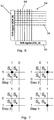
- the image capture device 2 includes a sensor 4 having an active area comprising a rectangular array of photosensitive picture elements (pixels) 6.
- the sensor 4 may for example be a CMOS APS device (a complementary metal-oxide semiconductor, active pixel sensor device), or equivalent.
- each pixel integrates the charge generated when photons strike its surface. After the set integration time T i , the charge on all the pixels is digitised and the resulting digital image data is transferred from the sensor 4 to a memory device.
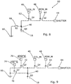
- the photosensor device 14 comprises a photodetector, for example a photodiode or phototransistor.
- the photosensor device 14 provides an output signal at photosensor connection 16, which is represented by voltage V p .
- This output signal is connected to a first terminal of the transistor transfer switch 18.
- a second terminal of the transfer switch 18 provides a readout connection 20 for a readout voltage V s and is connected to the readout circuit 22.
- the gate terminal of the transfer switch 18 is connected to receive a shutter signal from a shutter node 28.
- the transfer switch 18 is an n-channel MOSFET (metal oxide semiconductor field effect transistor), which only conducts when it receives an on signal from the shutter node 28.
- MOSFET metal oxide semiconductor field effect transistor
- control circuit 60 provides an on control signal at output connection 40 only when all three input signals are on. Therefore, the transfer switch 18 will only conduct when the shutter signal, the column select signal and the row select signal are all on. Operation of the pixel can be controlled by applying on and off signals to the column select node 46 and the row select node 48, and by applying the shutter signal to the shutter node 44. This allows each pixel in the pixel array to be activated individually, and makes it possible to capture a sequence of time-dependent lo-res image files as described above. These lo-res images can then be viewed separately in sequence or the data from all the pixels can be used to form a single hi-res image.
- a "movie/still” mode in which the pixel elements are actuated sequentially as described above, or a "still-only” mode in which all the pixel elements operate simultaneously.
- movie/still mode the captured los-res images can be viewed either sequentially as a movie, or together as a hi-res still image (possibly with some motion blur).
- still-only mode the motion blur will be equivalent to that of a conventional sensor, but because a set of time-separated lo-res images will not then be captured the possibility of viewing the images sequentially as a movie will not be available.
- the invention may be implemented within a camera that is intended primarily for capturing still images, to provide the possibility of capturing movies at a relatively high resolution and frame rate.
- a camera that can take a sequence of 8.2 megapixel images at a rate of five frames per second would be capable of providing a movie sequence of 0.8 megapixel images at a frame rate of fifty frames per second.
Applications Claiming Priority (2)
| Application Number | Priority Date | Filing Date | Title |
|---|---|---|---|
| GBGB1012631.6A GB201012631D0 (en) | 2010-07-28 | 2010-07-28 | Image sensor and method of sensing |
| PCT/GB2011/001051 WO2012013918A1 (en) | 2010-07-28 | 2011-07-12 | Image sensor and method of sensing |
Publications (2)
| Publication Number | Publication Date |
|---|---|
| EP2599300A1 EP2599300A1 (en) | 2013-06-05 |
| EP2599300B1 true EP2599300B1 (en) | 2020-02-19 |
Family
ID=42799205
Family Applications (1)
| Application Number | Title | Priority Date | Filing Date |
|---|---|---|---|
| EP11739130.0A Active EP2599300B1 (en) | 2010-07-28 | 2011-07-12 | Image sensor and method of sensing |
Country Status (5)
| Country | Link |
|---|---|
| US (1) | US9247167B2 (ja) |
| EP (1) | EP2599300B1 (ja) |
| JP (1) | JP5944387B2 (ja) |
| GB (1) | GB201012631D0 (ja) |
| WO (1) | WO2012013918A1 (ja) |
Families Citing this family (8)
| Publication number | Priority date | Publication date | Assignee | Title |
|---|---|---|---|---|
| US8786732B2 (en) | 2012-10-31 | 2014-07-22 | Pixon Imaging, Inc. | Device and method for extending dynamic range in an image sensor |
| US20140168415A1 (en) * | 2012-12-07 | 2014-06-19 | Magna Electronics Inc. | Vehicle vision system with micro lens array |
| CN106134181B (zh) * | 2014-03-24 | 2019-03-01 | 富士胶片株式会社 | 摄影装置 |
| US9819841B1 (en) * | 2015-04-17 | 2017-11-14 | Altera Corporation | Integrated circuits with optical flow computation circuitry |
| JP7042025B2 (ja) * | 2017-01-23 | 2022-03-25 | ソニーセミコンダクタソリューションズ株式会社 | 情報処理装置、情報処理方法、及び記録媒体 |
| GB2574619B (en) | 2018-06-12 | 2022-10-12 | Res & Innovation Uk | Image sensor |
| EP3614174B1 (en) * | 2018-08-21 | 2021-06-23 | Omron Corporation | Distance measuring device and distance measuring method |
| EP4235219A1 (en) | 2022-02-28 | 2023-08-30 | Imasenic Advanced Imaging, S.L. | Depth scanning image sensor |
Citations (1)
| Publication number | Priority date | Publication date | Assignee | Title |
|---|---|---|---|---|
| JP2006121151A (ja) * | 2004-10-19 | 2006-05-11 | Sony Corp | 信号処理方法および信号処理装置並びに物理情報取得装置 |
Family Cites Families (31)
| Publication number | Priority date | Publication date | Assignee | Title |
|---|---|---|---|---|
| US4574311A (en) | 1985-04-04 | 1986-03-04 | Thinking Machines Corporation | Random array sensing devices |
| KR100228424B1 (ko) * | 1996-06-29 | 1999-11-01 | 김영환 | 반도체 메모리 장치의 엑스 디코더 회로 |
| AU5457098A (en) * | 1997-08-15 | 1999-03-08 | Intel Corporation | Color channel independent electronic shutter for solid state image sensor |
| US6369853B1 (en) * | 1997-11-13 | 2002-04-09 | Foveon, Inc. | Intra-pixel frame storage element, array, and electronic shutter method suitable for electronic still camera applications |
| DE19928454B4 (de) * | 1998-06-29 | 2010-01-21 | Fujitsu Microelectronics Ltd. | Speichervorrichtung mit Reihendecodierer |
| JP3581953B2 (ja) * | 1999-07-26 | 2004-10-27 | 沖電気工業株式会社 | 半導体記憶装置 |
| JP3942332B2 (ja) * | 2000-01-07 | 2007-07-11 | 富士通株式会社 | 半導体記憶装置 |
| KR100359770B1 (ko) * | 2000-03-02 | 2002-11-04 | 주식회사 하이닉스반도체 | 씨모스 이미지 센서의 액티브 픽셀 회로 |
| US7268815B1 (en) * | 2000-10-06 | 2007-09-11 | Cypress Semiconductor Corporation (Belgium) Bvba | Differential readout of a pixel array with elimination of pixel- and column-wise fixed pattern noise |
| JP4356231B2 (ja) * | 2000-11-21 | 2009-11-04 | コニカミノルタホールディングス株式会社 | 走査回路及びそれを備えた撮像装置 |
| US6720592B1 (en) * | 2001-06-29 | 2004-04-13 | National Semiconductor Corp. | Apparatus for high sensitivity, low lag, high voltage swing in a pixel cell with an electronic shutter |
| US7106377B2 (en) * | 2001-07-25 | 2006-09-12 | Hewlett-Packard Development Company, L.P. | Image capturing device capable of single pixel exposure duration control |
| US7499091B2 (en) * | 2002-03-20 | 2009-03-03 | Sony Corporation | Solid-state imaging device and method for driving same |
| ITUD20020084A1 (it) * | 2002-04-12 | 2003-10-13 | Neuricam Spa | Dispositivo elettronico selezionatore per sensori elettro-ottici |
| KR100562489B1 (ko) * | 2002-11-11 | 2006-03-21 | 삼성전자주식회사 | 셔터 타이밍 조절 가능한 로우 디코더를 갖는 이미지 센서 |
| JP4687155B2 (ja) * | 2005-03-09 | 2011-05-25 | ソニー株式会社 | 固体撮像装置およびその駆動方法 |
| JP2007166238A (ja) * | 2005-12-14 | 2007-06-28 | Victor Co Of Japan Ltd | 画素別シャッタ機能付cmosセンサ |
| JP2008271186A (ja) * | 2007-04-20 | 2008-11-06 | Olympus Corp | 固体撮像装置 |
| GB0709026D0 (en) * | 2007-05-10 | 2007-06-20 | Isis Innovation | High speed imaging with slow scan cameras using pixel level dynami shuttering |
| JP5022108B2 (ja) * | 2007-06-01 | 2012-09-12 | ルネサスエレクトロニクス株式会社 | 半導体記憶装置及びそのテスト方法 |
| DE102007045448A1 (de) * | 2007-09-24 | 2009-04-02 | Arnold & Richter Cine Technik Gmbh & Co. Betriebs Kg | Bildsensor |
| JP4442675B2 (ja) * | 2007-09-28 | 2010-03-31 | ソニー株式会社 | 画素駆動回路および撮像装置ならびにカメラシステム |
| JP2009253559A (ja) * | 2008-04-03 | 2009-10-29 | Sharp Corp | 固体撮像装置および電子情報機器 |
| JP2009296477A (ja) * | 2008-06-09 | 2009-12-17 | Olympus Corp | 固体撮像装置 |
| US7889256B2 (en) * | 2008-06-11 | 2011-02-15 | Aptina Imaging Corporation | Method and apparatus for reducing temporal row-wise noise in imagers |
| JP5446282B2 (ja) * | 2009-01-21 | 2014-03-19 | ソニー株式会社 | 固体撮像素子およびカメラシステム |
| JP5661260B2 (ja) * | 2009-07-16 | 2015-01-28 | キヤノン株式会社 | 固体撮像装置及びその駆動方法 |
| JP5598126B2 (ja) * | 2010-07-09 | 2014-10-01 | ソニー株式会社 | 固体撮像素子およびカメラシステム |
| JP5999402B2 (ja) * | 2011-08-12 | 2016-09-28 | ソニー株式会社 | 固体撮像素子および製造方法、並びに電子機器 |
| US20130140442A1 (en) * | 2011-12-02 | 2013-06-06 | Sony Corporation | Amplifying circuit and manufacturing method, solid-state imaging element, and electronic device |
| JP2014187270A (ja) * | 2013-03-25 | 2014-10-02 | Sony Corp | 固体撮像装置およびその製造方法、並びに電子機器 |
-
2010
- 2010-07-28 GB GBGB1012631.6A patent/GB201012631D0/en not_active Ceased
-
2011
- 2011-07-12 EP EP11739130.0A patent/EP2599300B1/en active Active
- 2011-07-12 WO PCT/GB2011/001051 patent/WO2012013918A1/en active Application Filing
- 2011-07-12 JP JP2013521202A patent/JP5944387B2/ja active Active
- 2011-07-12 US US13/811,724 patent/US9247167B2/en active Active
Patent Citations (1)
| Publication number | Priority date | Publication date | Assignee | Title |
|---|---|---|---|---|
| JP2006121151A (ja) * | 2004-10-19 | 2006-05-11 | Sony Corp | 信号処理方法および信号処理装置並びに物理情報取得装置 |
Also Published As
| Publication number | Publication date |
|---|---|
| EP2599300A1 (en) | 2013-06-05 |
| JP5944387B2 (ja) | 2016-07-05 |
| US9247167B2 (en) | 2016-01-26 |
| US20130182160A1 (en) | 2013-07-18 |
| WO2012013918A1 (en) | 2012-02-02 |
| WO2012013918A4 (en) | 2012-03-08 |
| JP2013536625A (ja) | 2013-09-19 |
| GB201012631D0 (en) | 2010-09-15 |
Similar Documents
| Publication | Publication Date | Title |
|---|---|---|
| EP2599300B1 (en) | Image sensor and method of sensing | |
| EP2145467B1 (en) | Image capture device and method | |
| US11050955B2 (en) | Solid-state imaging device, method for driving solid-state imaging device, and electronic apparatus | |
| KR102632643B1 (ko) | 이미지 센서 및 전자 기기 | |
| US9438868B2 (en) | Adaptive image sensor systems and methods | |
| WO2013043259A1 (en) | Imaging system with foveated imaging capabilities | |
| EP2478558A1 (en) | Image sensor with wide dynamic range | |
| EP3378224A1 (en) | Image sensor system | |
| JP2013536625A5 (ja) | ||
| KR20030029124A (ko) | 전자 고분해능 디지털 스틸 카메라 | |
| US9282245B2 (en) | Image capturing apparatus and method of controlling the same | |
| JP7433792B2 (ja) | 撮像装置およびその制御方法 | |
| JP2019103121A (ja) | 撮像素子、撮像装置及び撮像方法 | |
| JP2020028115A (ja) | 撮像装置 | |
| JP2017194280A (ja) | 撮像回路、信号読出回路、赤外線撮像装置、赤外線検出回路および撮像回路の動作方法 | |
| WO2019216029A1 (ja) | 撮像装置、電子機器および駆動方法 | |
| JP2005303546A (ja) | 撮像装置及び撮像素子の駆動方法 | |
| WO2013030561A1 (en) | Pixel circuit |
Legal Events
| Date | Code | Title | Description |
|---|---|---|---|
| PUAI | Public reference made under article 153(3) epc to a published international application that has entered the european phase |
Free format text: ORIGINAL CODE: 0009012 |
|
| 17P | Request for examination filed |
Effective date: 20130125 |
|
| AK | Designated contracting states |
Kind code of ref document: A1 Designated state(s): AL AT BE BG CH CY CZ DE DK EE ES FI FR GB GR HR HU IE IS IT LI LT LU LV MC MK MT NL NO PL PT RO RS SE SI SK SM TR |
|
| DAX | Request for extension of the european patent (deleted) | ||
| RAP1 | Party data changed (applicant data changed or rights of an application transferred) |
Owner name: OXFORD UNIVERSITY INNOVATION LIMITED |
|
| RAP1 | Party data changed (applicant data changed or rights of an application transferred) |
Owner name: OXFORD UNIVERSITY INNOVATION LIMITED |
|
| STAA | Information on the status of an ep patent application or granted ep patent |
Free format text: STATUS: EXAMINATION IS IN PROGRESS |
|
| 17Q | First examination report despatched |
Effective date: 20170508 |
|
| REG | Reference to a national code |
Ref country code: DE Ref legal event code: R079 Ref document number: 602011065085 Country of ref document: DE Free format text: PREVIOUS MAIN CLASS: H04N0005232000 Ipc: H04N0005345000 |
|
| GRAP | Despatch of communication of intention to grant a patent |
Free format text: ORIGINAL CODE: EPIDOSNIGR1 |
|
| STAA | Information on the status of an ep patent application or granted ep patent |
Free format text: STATUS: GRANT OF PATENT IS INTENDED |
|
| RIC1 | Information provided on ipc code assigned before grant |
Ipc: H04N 5/343 20110101ALI20190819BHEP Ipc: H04N 5/345 20110101AFI20190819BHEP Ipc: H04N 5/3745 20110101ALI20190819BHEP Ipc: H04N 5/353 20110101ALI20190819BHEP |
|
| INTG | Intention to grant announced |
Effective date: 20190919 |
|
| GRAS | Grant fee paid |
Free format text: ORIGINAL CODE: EPIDOSNIGR3 |
|
| GRAA | (expected) grant |
Free format text: ORIGINAL CODE: 0009210 |
|
| STAA | Information on the status of an ep patent application or granted ep patent |
Free format text: STATUS: THE PATENT HAS BEEN GRANTED |
|
| AK | Designated contracting states |
Kind code of ref document: B1 Designated state(s): AL AT BE BG CH CY CZ DE DK EE ES FI FR GB GR HR HU IE IS IT LI LT LU LV MC MK MT NL NO PL PT RO RS SE SI SK SM TR |
|
| REG | Reference to a national code |
Ref country code: GB Ref legal event code: FG4D |
|
| REG | Reference to a national code |
Ref country code: CH Ref legal event code: EP |
|
| REG | Reference to a national code |
Ref country code: DE Ref legal event code: R096 Ref document number: 602011065085 Country of ref document: DE |
|
| REG | Reference to a national code |
Ref country code: AT Ref legal event code: REF Ref document number: 1236307 Country of ref document: AT Kind code of ref document: T Effective date: 20200315 |
|
| REG | Reference to a national code |
Ref country code: IE Ref legal event code: FG4D |
|
| REG | Reference to a national code |
Ref country code: NL Ref legal event code: FP |
|
| PG25 | Lapsed in a contracting state [announced via postgrant information from national office to epo] |
Ref country code: FI Free format text: LAPSE BECAUSE OF FAILURE TO SUBMIT A TRANSLATION OF THE DESCRIPTION OR TO PAY THE FEE WITHIN THE PRESCRIBED TIME-LIMIT Effective date: 20200219 Ref country code: NO Free format text: LAPSE BECAUSE OF FAILURE TO SUBMIT A TRANSLATION OF THE DESCRIPTION OR TO PAY THE FEE WITHIN THE PRESCRIBED TIME-LIMIT Effective date: 20200519 Ref country code: RS Free format text: LAPSE BECAUSE OF FAILURE TO SUBMIT A TRANSLATION OF THE DESCRIPTION OR TO PAY THE FEE WITHIN THE PRESCRIBED TIME-LIMIT Effective date: 20200219 |
|
| REG | Reference to a national code |
Ref country code: LT Ref legal event code: MG4D |
|
| PG25 | Lapsed in a contracting state [announced via postgrant information from national office to epo] |
Ref country code: IS Free format text: LAPSE BECAUSE OF FAILURE TO SUBMIT A TRANSLATION OF THE DESCRIPTION OR TO PAY THE FEE WITHIN THE PRESCRIBED TIME-LIMIT Effective date: 20200619 Ref country code: GR Free format text: LAPSE BECAUSE OF FAILURE TO SUBMIT A TRANSLATION OF THE DESCRIPTION OR TO PAY THE FEE WITHIN THE PRESCRIBED TIME-LIMIT Effective date: 20200520 Ref country code: BG Free format text: LAPSE BECAUSE OF FAILURE TO SUBMIT A TRANSLATION OF THE DESCRIPTION OR TO PAY THE FEE WITHIN THE PRESCRIBED TIME-LIMIT Effective date: 20200519 Ref country code: SE Free format text: LAPSE BECAUSE OF FAILURE TO SUBMIT A TRANSLATION OF THE DESCRIPTION OR TO PAY THE FEE WITHIN THE PRESCRIBED TIME-LIMIT Effective date: 20200219 Ref country code: LV Free format text: LAPSE BECAUSE OF FAILURE TO SUBMIT A TRANSLATION OF THE DESCRIPTION OR TO PAY THE FEE WITHIN THE PRESCRIBED TIME-LIMIT Effective date: 20200219 Ref country code: HR Free format text: LAPSE BECAUSE OF FAILURE TO SUBMIT A TRANSLATION OF THE DESCRIPTION OR TO PAY THE FEE WITHIN THE PRESCRIBED TIME-LIMIT Effective date: 20200219 |
|
| PG25 | Lapsed in a contracting state [announced via postgrant information from national office to epo] |
Ref country code: ES Free format text: LAPSE BECAUSE OF FAILURE TO SUBMIT A TRANSLATION OF THE DESCRIPTION OR TO PAY THE FEE WITHIN THE PRESCRIBED TIME-LIMIT Effective date: 20200219 Ref country code: DK Free format text: LAPSE BECAUSE OF FAILURE TO SUBMIT A TRANSLATION OF THE DESCRIPTION OR TO PAY THE FEE WITHIN THE PRESCRIBED TIME-LIMIT Effective date: 20200219 Ref country code: SK Free format text: LAPSE BECAUSE OF FAILURE TO SUBMIT A TRANSLATION OF THE DESCRIPTION OR TO PAY THE FEE WITHIN THE PRESCRIBED TIME-LIMIT Effective date: 20200219 Ref country code: RO Free format text: LAPSE BECAUSE OF FAILURE TO SUBMIT A TRANSLATION OF THE DESCRIPTION OR TO PAY THE FEE WITHIN THE PRESCRIBED TIME-LIMIT Effective date: 20200219 Ref country code: PT Free format text: LAPSE BECAUSE OF FAILURE TO SUBMIT A TRANSLATION OF THE DESCRIPTION OR TO PAY THE FEE WITHIN THE PRESCRIBED TIME-LIMIT Effective date: 20200712 Ref country code: LT Free format text: LAPSE BECAUSE OF FAILURE TO SUBMIT A TRANSLATION OF THE DESCRIPTION OR TO PAY THE FEE WITHIN THE PRESCRIBED TIME-LIMIT Effective date: 20200219 Ref country code: EE Free format text: LAPSE BECAUSE OF FAILURE TO SUBMIT A TRANSLATION OF THE DESCRIPTION OR TO PAY THE FEE WITHIN THE PRESCRIBED TIME-LIMIT Effective date: 20200219 Ref country code: SM Free format text: LAPSE BECAUSE OF FAILURE TO SUBMIT A TRANSLATION OF THE DESCRIPTION OR TO PAY THE FEE WITHIN THE PRESCRIBED TIME-LIMIT Effective date: 20200219 Ref country code: CZ Free format text: LAPSE BECAUSE OF FAILURE TO SUBMIT A TRANSLATION OF THE DESCRIPTION OR TO PAY THE FEE WITHIN THE PRESCRIBED TIME-LIMIT Effective date: 20200219 |
|
| REG | Reference to a national code |
Ref country code: AT Ref legal event code: MK05 Ref document number: 1236307 Country of ref document: AT Kind code of ref document: T Effective date: 20200219 |
|
| REG | Reference to a national code |
Ref country code: DE Ref legal event code: R097 Ref document number: 602011065085 Country of ref document: DE |
|
| PLBE | No opposition filed within time limit |
Free format text: ORIGINAL CODE: 0009261 |
|
| STAA | Information on the status of an ep patent application or granted ep patent |
Free format text: STATUS: NO OPPOSITION FILED WITHIN TIME LIMIT |
|
| 26N | No opposition filed |
Effective date: 20201120 |
|
| PG25 | Lapsed in a contracting state [announced via postgrant information from national office to epo] |
Ref country code: IT Free format text: LAPSE BECAUSE OF FAILURE TO SUBMIT A TRANSLATION OF THE DESCRIPTION OR TO PAY THE FEE WITHIN THE PRESCRIBED TIME-LIMIT Effective date: 20200219 Ref country code: AT Free format text: LAPSE BECAUSE OF FAILURE TO SUBMIT A TRANSLATION OF THE DESCRIPTION OR TO PAY THE FEE WITHIN THE PRESCRIBED TIME-LIMIT Effective date: 20200219 |
|
| PG25 | Lapsed in a contracting state [announced via postgrant information from national office to epo] |
Ref country code: SI Free format text: LAPSE BECAUSE OF FAILURE TO SUBMIT A TRANSLATION OF THE DESCRIPTION OR TO PAY THE FEE WITHIN THE PRESCRIBED TIME-LIMIT Effective date: 20200219 Ref country code: PL Free format text: LAPSE BECAUSE OF FAILURE TO SUBMIT A TRANSLATION OF THE DESCRIPTION OR TO PAY THE FEE WITHIN THE PRESCRIBED TIME-LIMIT Effective date: 20200219 Ref country code: MC Free format text: LAPSE BECAUSE OF FAILURE TO SUBMIT A TRANSLATION OF THE DESCRIPTION OR TO PAY THE FEE WITHIN THE PRESCRIBED TIME-LIMIT Effective date: 20200219 |
|
| REG | Reference to a national code |
Ref country code: CH Ref legal event code: PL |
|
| REG | Reference to a national code |
Ref country code: BE Ref legal event code: MM Effective date: 20200731 |
|
| PG25 | Lapsed in a contracting state [announced via postgrant information from national office to epo] |
Ref country code: CH Free format text: LAPSE BECAUSE OF NON-PAYMENT OF DUE FEES Effective date: 20200731 Ref country code: LI Free format text: LAPSE BECAUSE OF NON-PAYMENT OF DUE FEES Effective date: 20200731 Ref country code: LU Free format text: LAPSE BECAUSE OF NON-PAYMENT OF DUE FEES Effective date: 20200712 |
|
| PG25 | Lapsed in a contracting state [announced via postgrant information from national office to epo] |
Ref country code: BE Free format text: LAPSE BECAUSE OF NON-PAYMENT OF DUE FEES Effective date: 20200731 |
|
| PG25 | Lapsed in a contracting state [announced via postgrant information from national office to epo] |
Ref country code: IE Free format text: LAPSE BECAUSE OF NON-PAYMENT OF DUE FEES Effective date: 20200712 |
|
| PG25 | Lapsed in a contracting state [announced via postgrant information from national office to epo] |
Ref country code: TR Free format text: LAPSE BECAUSE OF FAILURE TO SUBMIT A TRANSLATION OF THE DESCRIPTION OR TO PAY THE FEE WITHIN THE PRESCRIBED TIME-LIMIT Effective date: 20200219 Ref country code: MT Free format text: LAPSE BECAUSE OF FAILURE TO SUBMIT A TRANSLATION OF THE DESCRIPTION OR TO PAY THE FEE WITHIN THE PRESCRIBED TIME-LIMIT Effective date: 20200219 Ref country code: CY Free format text: LAPSE BECAUSE OF FAILURE TO SUBMIT A TRANSLATION OF THE DESCRIPTION OR TO PAY THE FEE WITHIN THE PRESCRIBED TIME-LIMIT Effective date: 20200219 |
|
| PG25 | Lapsed in a contracting state [announced via postgrant information from national office to epo] |
Ref country code: MK Free format text: LAPSE BECAUSE OF FAILURE TO SUBMIT A TRANSLATION OF THE DESCRIPTION OR TO PAY THE FEE WITHIN THE PRESCRIBED TIME-LIMIT Effective date: 20200219 Ref country code: AL Free format text: LAPSE BECAUSE OF FAILURE TO SUBMIT A TRANSLATION OF THE DESCRIPTION OR TO PAY THE FEE WITHIN THE PRESCRIBED TIME-LIMIT Effective date: 20200219 |
|
| REG | Reference to a national code |
Ref country code: DE Ref legal event code: R079 Ref document number: 602011065085 Country of ref document: DE Free format text: PREVIOUS MAIN CLASS: H04N0005345000 Ipc: H04N0025440000 |
|
| P01 | Opt-out of the competence of the unified patent court (upc) registered |
Effective date: 20230525 |
|
| PGFP | Annual fee paid to national office [announced via postgrant information from national office to epo] |
Ref country code: NL Payment date: 20230704 Year of fee payment: 13 |
|
| PGFP | Annual fee paid to national office [announced via postgrant information from national office to epo] |
Ref country code: GB Payment date: 20230718 Year of fee payment: 13 |
|
| PGFP | Annual fee paid to national office [announced via postgrant information from national office to epo] |
Ref country code: FR Payment date: 20230718 Year of fee payment: 13 Ref country code: DE Payment date: 20230704 Year of fee payment: 13 |