EP2599300B1 - Image sensor and method of sensing - Google Patents
Image sensor and method of sensing Download PDFInfo
- Publication number
- EP2599300B1 EP2599300B1 EP11739130.0A EP11739130A EP2599300B1 EP 2599300 B1 EP2599300 B1 EP 2599300B1 EP 11739130 A EP11739130 A EP 11739130A EP 2599300 B1 EP2599300 B1 EP 2599300B1
- Authority
- EP
- European Patent Office
- Prior art keywords
- pixel
- pixels
- select signal
- signal
- image
- Prior art date
- Legal status (The legal status is an assumption and is not a legal conclusion. Google has not performed a legal analysis and makes no representation as to the accuracy of the status listed.)
- Active
Links
- 238000000034 method Methods 0.000 title claims description 15
- 230000001960 triggered effect Effects 0.000 claims description 9
- 238000013500 data storage Methods 0.000 claims description 4
- 230000011664 signaling Effects 0.000 claims 1
- 238000010586 diagram Methods 0.000 description 6
- 230000010354 integration Effects 0.000 description 5
- 238000004422 calculation algorithm Methods 0.000 description 4
- 238000003384 imaging method Methods 0.000 description 4
- 229910044991 metal oxide Inorganic materials 0.000 description 2
- 150000004706 metal oxides Chemical class 0.000 description 2
- 238000012544 monitoring process Methods 0.000 description 2
- 230000003287 optical effect Effects 0.000 description 2
- 239000004065 semiconductor Substances 0.000 description 2
- 230000002123 temporal effect Effects 0.000 description 2
- 230000036962 time dependent Effects 0.000 description 2
- 238000012152 algorithmic method Methods 0.000 description 1
- 230000003321 amplification Effects 0.000 description 1
- 230000000295 complement effect Effects 0.000 description 1
- 230000007423 decrease Effects 0.000 description 1
- 230000003247 decreasing effect Effects 0.000 description 1
- 238000001514 detection method Methods 0.000 description 1
- 230000000694 effects Effects 0.000 description 1
- 230000005669 field effect Effects 0.000 description 1
- 230000006870 function Effects 0.000 description 1
- 230000001788 irregular Effects 0.000 description 1
- 238000003199 nucleic acid amplification method Methods 0.000 description 1
- 239000007787 solid Substances 0.000 description 1
- 230000003068 static effect Effects 0.000 description 1
Images


Classifications
-
- H—ELECTRICITY
- H04—ELECTRIC COMMUNICATION TECHNIQUE
- H04N—PICTORIAL COMMUNICATION, e.g. TELEVISION
- H04N25/00—Circuitry of solid-state image sensors [SSIS]; Control thereof
- H04N25/50—Control of the SSIS exposure
- H04N25/53—Control of the integration time
-
- H—ELECTRICITY
- H04—ELECTRIC COMMUNICATION TECHNIQUE
- H04N—PICTORIAL COMMUNICATION, e.g. TELEVISION
- H04N25/00—Circuitry of solid-state image sensors [SSIS]; Control thereof
- H04N25/40—Extracting pixel data from image sensors by controlling scanning circuits, e.g. by modifying the number of pixels sampled or to be sampled
- H04N25/42—Extracting pixel data from image sensors by controlling scanning circuits, e.g. by modifying the number of pixels sampled or to be sampled by switching between different modes of operation using different resolutions or aspect ratios, e.g. switching between interlaced and non-interlaced mode
-
- H—ELECTRICITY
- H04—ELECTRIC COMMUNICATION TECHNIQUE
- H04N—PICTORIAL COMMUNICATION, e.g. TELEVISION
- H04N25/00—Circuitry of solid-state image sensors [SSIS]; Control thereof
- H04N25/40—Extracting pixel data from image sensors by controlling scanning circuits, e.g. by modifying the number of pixels sampled or to be sampled
- H04N25/44—Extracting pixel data from image sensors by controlling scanning circuits, e.g. by modifying the number of pixels sampled or to be sampled by partially reading an SSIS array
- H04N25/445—Extracting pixel data from image sensors by controlling scanning circuits, e.g. by modifying the number of pixels sampled or to be sampled by partially reading an SSIS array by skipping some contiguous pixels within the read portion of the array
-
- H—ELECTRICITY
- H04—ELECTRIC COMMUNICATION TECHNIQUE
- H04N—PICTORIAL COMMUNICATION, e.g. TELEVISION
- H04N25/00—Circuitry of solid-state image sensors [SSIS]; Control thereof
- H04N25/70—SSIS architectures; Circuits associated therewith
- H04N25/76—Addressed sensors, e.g. MOS or CMOS sensors
- H04N25/77—Pixel circuitry, e.g. memories, A/D converters, pixel amplifiers, shared circuits or shared components
Definitions
- the pixels By triggering the pixels individually, it is possible to capture either a single hi-res image using all the pixels, or one or more lo-res images using fewer than all the pixels.
- the pixels can be triggered electronically, thus avoiding the need for a separate shutter array. The size and complexity of the device are thus significantly reduced.
- the pixels are arranged in an array of rows and columns and are connected to receive a row select signal and a column select signal, whereby an individual pixel can be selected by transmitting a row select signal and a column select signal along the row and the column in which that pixel is located.
- This arrangement allows each pixel to be selected individually without the need for individual control lines. This therefore avoids excessive circuit complexity.
- the rows and columns may be either orthogonal or non-orthogonal.
- the pixels are arranged in an array of rows and columns and an individual pixel is selected by transmitting a row select signal and a column select signal along the row and the column in which that pixel is located.
- the image capture device 2 includes a sensor 4 having an active area comprising a rectangular array of photosensitive picture elements (pixels) 6.
- the sensor 4 may for example be a CMOS APS device (a complementary metal-oxide semiconductor, active pixel sensor device), or equivalent.
- each pixel integrates the charge generated when photons strike its surface. After the set integration time T i , the charge on all the pixels is digitised and the resulting digital image data is transferred from the sensor 4 to a memory device.
- the photosensor device 14 comprises a photodetector, for example a photodiode or phototransistor.
- the photosensor device 14 provides an output signal at photosensor connection 16, which is represented by voltage V p .
- This output signal is connected to a first terminal of the transistor transfer switch 18.
- a second terminal of the transfer switch 18 provides a readout connection 20 for a readout voltage V s and is connected to the readout circuit 22.
- the gate terminal of the transfer switch 18 is connected to receive a shutter signal from a shutter node 28.
- the transfer switch 18 is an n-channel MOSFET (metal oxide semiconductor field effect transistor), which only conducts when it receives an on signal from the shutter node 28.
- MOSFET metal oxide semiconductor field effect transistor
- control circuit 60 provides an on control signal at output connection 40 only when all three input signals are on. Therefore, the transfer switch 18 will only conduct when the shutter signal, the column select signal and the row select signal are all on. Operation of the pixel can be controlled by applying on and off signals to the column select node 46 and the row select node 48, and by applying the shutter signal to the shutter node 44. This allows each pixel in the pixel array to be activated individually, and makes it possible to capture a sequence of time-dependent lo-res image files as described above. These lo-res images can then be viewed separately in sequence or the data from all the pixels can be used to form a single hi-res image.
- a "movie/still” mode in which the pixel elements are actuated sequentially as described above, or a "still-only” mode in which all the pixel elements operate simultaneously.
- movie/still mode the captured los-res images can be viewed either sequentially as a movie, or together as a hi-res still image (possibly with some motion blur).
- still-only mode the motion blur will be equivalent to that of a conventional sensor, but because a set of time-separated lo-res images will not then be captured the possibility of viewing the images sequentially as a movie will not be available.
- the invention may be implemented within a camera that is intended primarily for capturing still images, to provide the possibility of capturing movies at a relatively high resolution and frame rate.
- a camera that can take a sequence of 8.2 megapixel images at a rate of five frames per second would be capable of providing a movie sequence of 0.8 megapixel images at a frame rate of fifty frames per second.
Description
- The present invention relates to an image sensor and to an image capture device. The invention also relates to a method of capturing images. In particular but not exclusively, the invention relates to a device and method for capturing both still and moving images (movies).
- Electronic cameras are generally divided into two broad categories: still cameras and video cameras. However, there is a degree of overlap between the two types of camera. For example, some "video" cameras are capable of capturing both movies and still images.
- On the other hand, some still cameras are provided with a "movie" or "video" function, which allows the camera to capture a sequence of images. These images can subsequently be shown as a movie. This invention is concerned primarily (but not exclusively) with the latter type of camera.
- Electronic cameras generally include an image capture device or sensor having an array of photosensitive detectors or picture elements (pixels). A moving image or movie can be captured by recording a sequence of images detected by the sensor.
- The rate at which a sequence of images can be captured (the frame rate) depends in part on the size of the sensor (that is, the number of pixels in the array), and is limited by the rate at which data can be read (digitised) from the sensor. Reading information from an imaging sensor at high speed introduces noise (read noise), which lowers the signal quality of the image. Accordingly, if the sensor has a large number of pixels, the frame rate will generally be rather slow. Smaller sensors with fewer pixels may provide a higher frame rate, but the resolution of the image will be correspondingly reduced.
- The inventor's previous patent application
WO 2008/138543A describes an image capture device including a sensor with an active area comprising a plurality of pixels, and a shutter array comprising a plurality of shutter elements that can be activated individually to control the exposure of the individual pixels. The pixels are arranged in a number of pixel S-P552354PC_110630 subsets that can be exposed sequentially to capture a sequence of lo-res images each comprising less than the full set of pixels, or simultaneously to capture a hi-res image comprising all or substantially all of the pixels. However, the provision of a separate shutter array adds to the size and complexity of the device. -
JP 2006 121151 A - It is an object of the present invention to provide an image sensor and a method of capturing images that mitigate at least some of the aforesaid disadvantages.
- According to one aspect of the invention there is provided an image sensor as defined by
claim 1. - By triggering the pixels individually, it is possible to capture either a single hi-res image using all the pixels, or one or more lo-res images using fewer than all the pixels. The pixels can be triggered electronically, thus avoiding the need for a separate shutter array. The size and complexity of the device are thus significantly reduced.
- Advantageously, the pixels are arranged in an array of rows and columns and are connected to receive a row select signal and a column select signal, whereby an individual pixel can be selected by transmitting a row select signal and a column select signal along the row and the column in which that pixel is located. This arrangement allows each pixel to be selected individually without the need for individual control lines. This therefore avoids excessive circuit complexity. The rows and columns may be either orthogonal or non-orthogonal.
- Preferably, the selection means comprises a plurality of row selection lines and a plurality of column selection lines, wherein each row selection line is connected to all the pixels in a particular row and each column selection line is connected to all the pixels in a particular column. Thus it is possible to select all of the pixels individually using just two sets of control connections. The selection means preferably comprises a grid of row selection connections and column selection connections.
- Advantageously, at least one of the row select signal and the column select signal is generated by a shift register. Preferably, both the row select signal and the column select signal are generated by shift registers. A shift register is an electronic device that can store a series of digital values and can shift that sequence backwards and forwards. This allows the pixels to be triggered in a predetermined sequence. The digital values held in the shift registers can also be modified very easily to change the sequence in which the pixels are triggered. This makes it possible to adjust the number of pixels exposed at any one time, and the order in which the pixels are exposed.
- Advantageously, each pixel includes a control means for triggering the pixel, the control means being constructed and arranged to trigger the pixel only when it receives simultaneously a shutter signal, a row select signal and a column select signal.
- In one embodiment, the control means includes a logical AND gate having inputs for receiving a shutter signal, a row select signal and a column select signal.
- In another embodiment, the control means includes a plurality of series-connected switch devices, each switch device being operably connected to receive at least one of a shutter signal, a row select signal and a column select signal. This arrangement is preferred in some situations to the use of an AND gate as it requires fewer transistors and therefore occupies less area on the surface of the sensor device. The switch devices may for example be transistor pass switches, for example MOSFET transistors.
- The image sensor preferably comprises a CMOS APS device, in which each pixel includes a device for storing an electrical charge representing the amount of light falling on the pixel. This allows each pixel to store a charge representing the incident light until all of the pixels have been exposed, after which the data from all of the pixels can be captured. This increases the operational speed of the device.
- According to another aspect, the invention comprises an image capture device including an image sensor according to any one of the preceding statements of invention and a data storage device for storing data from the pixels, said pixels being divided into a plurality of pixel subsets and said image capture device being constructed and arranged to capture a plurality of time-separated lo-res images, each said lo-res image comprising the data from a different pixel subset.
- Advantageously, the image capture device is constructed and arranged to capture a hi-res image using data from all the pixels on the sensor to create a full frame, high resolution image.
- The image capture device may include a control device for controlling operation of the pixel array, wherein the control device is constructed and arranged to trigger the pixels in a predefined, random or pseudo-random sequence.
- According to another aspect, the invention comprises a camera that includes an image capture device according to any one of the preceding statements of invention. The camera preferably includes a lens for focussing light onto the active area of the sensor. The camera may also include a display device for displaying captured images, which is constructed and arranged to display either a single hi-res image or a sequence of lo-res images. Advantageously, the camera includes a control device for controlling the exposure of the pixel subsets.
- According to another aspect of the invention there is provided a method of capturing images as defined by claim 10.
- The pixels in the array are triggered individually to capture light at different times.
- Preferably, the pixels are arranged in an array of rows and columns and an individual pixel is selected by transmitting a row select signal and a column select signal along the row and the column in which that pixel is located.
- Preferably, at least one of the row select signal and the column select signal is generated by a shift register.
- Preferably, each pixel is triggered to sense incident light only when it receives simultaneously a shutter signal, a row select signal and a column select signal. Advantageously, the method includes capturing a plurality of time-separated lo-res images, each lo-res image comprising the data from a different one of a plurality of pixel subsets.
- The pixel subsets are preferably exposed sequentially.
- Advantageously, a hi-res image is generated by combining the data from a plurality of lo-res images.
- The invention allows a set of time-separated low resolution ("lo-res") images to be embedded within each high resolution ("hi-res") image. The embedded lo-res images can then be viewed in sequence as a movie, or the data from all the pixels can be used to form a single hi-res image. Movies and still images can thus be captured simultaneously. The invention allows movies to be captured at much higher frame rates than can currently be achieved with existing sensor devices and, although the spatial resolution of the lo-res images is lower than that of the hi-res image, it is still sufficient for many purposes. The balance of resolution versus frame rate can be easily adjusted. Furthermore, the still images can be captured with no loss of spatial resolution and no significant increase in the data storage requirements of the device.
- Certain embodiments of the invention will now be described by way of example with reference to the accompanying drawings, in which:
-
Figure 1 is a front view showing schematically a small portion of an image sensor according to a first embodiment of the invention; -
Figure 2 is a chart illustrating shutter exposure times for respective shutter elements in the image capture device ofFigure 1 ; -
Figure 3 illustrates how a sequence of images may be captured by the image sensor; -
Figure 4 is a circuit diagram of a conventional prior art pixel with a global shutter control; -
Figure 5 is a circuit diagram of a pixel according to a first embodiment of the invention, with an individual pixel-level shutter control; -
Figure 6 illustrates a control circuit for a pixel according to an embodiment of the invention; -
Figure 7 illustrates schematically operation of the control circuit; -
Figure 8 is a circuit diagram of a pixel according to a second embodiment of the invention, with an individual pixel-level shutter control; -
Figure 9 is a circuit diagram of a pixel according to a third embodiment of the invention, with an individual pixel-level shutter control; and -
Figure 10 is a schematic diagram illustrating the main components of a camera that includes an image sensor according to the invention. - A portion of an image capture device according to a first embodiment of the invention is shown in
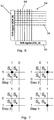
Figures 1 to 3 . Theimage capture device 2 includes asensor 4 having an active area comprising a rectangular array of photosensitive picture elements (pixels) 6. Thesensor 4 may for example be a CMOS APS device (a complementary metal-oxide semiconductor, active pixel sensor device), or equivalent. - For simplicity, the
sensor 4 shown infigure 1 is very small having only thirty-six pixels arranged in six by six pixel square array. In most real sensors the pixel array will be much larger than this and may consist of several million pixels. The pixel array may also have a different aspect ratio and the pixels may be arranged in various different patterns. - More generally, the
sensor 4 contains A pixels, which are divided into N subsets of pixels, which we will call subset S1, subset S2 ... subset SN. Each subset contains A/N pixels. In the simple example shown infigure 1 , the sensor has thirty-six pixels (A) and four subsets (N) of pixels, each subset containing nine pixels. - The
pixels 6 of the different subsets S1 to SN are grouped in a number ofpixel groups 8, eachpixel group 8 containing one pixel from each subset. In the example shown infigure 1 , eachpixel group 8 contains fourpixels 6, which are arranged in a square with a pixel from subset S1 in the top left corner, a pixel from subset S2 in the top right corner, pixel from subset S3 in the bottom left corner and pixel from subset S4 in the bottom right corner. Therefore, in this example thesensor 4 comprises four pixel subsets S1 to S4 and ninepixel groups 8. Thepixel groups 8 cover substantially the entire active surface of thesensor 4 and therefore each pixel subset S1 to SN includes pixels from substantially the entire active area of thesensor 4. - The
pixels 6 in each subset S1 to SN are electronically linked so that all the pixels in any one subset can be triggered to capture the incident light substantially simultaneously, the exposure of the pixels being controlled by control electronics as described in more detail below. In this example, the four pixel subsets S1 to S4 are arranged to capture light sequentially as shown inFigure 2 . Thus, the pixels in pixel subset S1 capture light for a first period 0.25 seconds, followed by the pixels in subset S2 for the next period 0.25 seconds, then the pixels of subset S3 for another 0.25 seconds and finally the pixels of subset S4 for a fourth period of 0.25 seconds. The total integration time Ti for all four pixel subsets S1 to S4 is therefore 1.0 second, the individual exposure time of each pixel being Ti/N (in this example, 0.25 seconds). - During exposure, each pixel integrates the charge generated when photons strike its surface. After the set integration time Ti, the charge on all the pixels is digitised and the resulting digital image data is transferred from the
sensor 4 to a memory device. - The stored image data may be displayed either as a moving image (a movie) comprising a sequence of successive images, or as a single still image. To display the image data as a movie, a separate image is created from the image data captured by each pixel subset. Thus, as illustrated in
Figure 3 , a first image I1 is created from the image data captured by all of the pixels in pixel subset S1 and represents the light incident on the sensor during the first period of 0.25 seconds. Image I2 is created from the image data captured by all the pixels in pixel subset S2 and represents the light incident on the sensor during the second period of 0.25 seconds, and so on for images I3 and I4. The four images I1 to L4 are then displayed sequentially, as a four frame video sequence. - When generating the movie, the apparent location of each pixel in the displayed low resolution image may be shifted slightly to take account of the fact that the pixels of the different pixel subsets collect data from slightly different, but known, locations. In this example, each frame of the movie has an image size of nine pixels, which is one quarter of the resolution of the entire sensor. We refer to images that are generated using less than the full pixel set as low resolution ("lo-res") images to distinguish them from high resolution ("hi-res") images generated using substantially the full pixel set. More specifically, a lo-res image is normally generated using a
fraction 1/N of the full pixel set, where N is an integer representing the number of pixel subsets. - If an extended video sequence is required, this image capture process may be repeated one or more times, with multiple data sets being captured at a rate of one data set every Ti seconds, and the captured lo-res images can subsequently be displayed in sequence.
- To display a still image, the data from all the pixels on the sensor is used to create a full frame, high resolution image. In this example, this will be a thirty-six pixel image.
- A circuit diagram for a conventional
prior art pixel 12 is shown inFigure 4 . A typical CMOS APS image sensor for a camera generally includes an array of such pixels. Thepixel 12 includes aphotosensor device 14, atransistor transfer switch 18, areadout circuit 22 and atransistor reset switch 24. - The
photosensor device 14 comprises a photodetector, for example a photodiode or phototransistor. Thephotosensor device 14 provides an output signal atphotosensor connection 16, which is represented by voltage Vp. This output signal is connected to a first terminal of thetransistor transfer switch 18. A second terminal of thetransfer switch 18 provides areadout connection 20 for a readout voltage Vs and is connected to thereadout circuit 22. The gate terminal of thetransfer switch 18 is connected to receive a shutter signal from ashutter node 28. In this example, thetransfer switch 18 is an n-channel MOSFET (metal oxide semiconductor field effect transistor), which only conducts when it receives an on signal from theshutter node 28. - The
reset switch 24 comprises another MOSFET transistor. In this example, the source terminal of thereset switch 24 is connected to a fixed power supply voltage Vdd . The gate terminal of thereset switch 24 is connected to receive a reset signal from areset node 30. The drain terminal is connected to thephotosensor device 14 throughphotosensor connection 16. - The
readout circuit 22 comprises a conventional selectable source-follower readout circuit, which includes a source-follower transistor 32, aselect transistor 34 connected to receive a rowselect signal 36, and anoutput node 38 for an output signal Vout, which is connected to the source connection of theselect transistor 34. Thereadout circuit 22 is designed to sense the voltage at thereadout connection 20 of thetransfer switch 18. The gate of theselect transistor 34 is connected to receive a select signal from a rowselect node 36 that selects which pixel in a column of pixels is connected to theoutput node 38. - In use, a reset signal is applied through the
reset node 30 to the gate of thetransistor reset switch 24, thus causing thereset switch 24 to conduct. Thereset switch 24 applies a high voltage Vdd to thephotosensor 14, which stores a charge owing to the intrinsic capacitance of the circuit components. Having reset the pixel, the reset signal then turns off. - In order to sense the intensity of the light falling on the pixel, an on signal is applied via the
shutter node 28 to the gate of thetransfer switch 18. This allows the stored charge to discharge through thephotodetector 14. The rate at which the charge discharges depends on the photocurrent Ip through thephotodetector 14, which in turn depends on the intensity of light incident on the photodetector. The voltage Vp atphotosensor connection 16 thus decreases at a rate that depends on the intensity of light falling on thephotosensor 14. - The photosensor 14 thus provides an output signal Vp at
photosensor connection 16 that is proportional to a time integral of the detected light. This output signal Vp is applied to the input of thereadout circuit 22 viatransfer switch 18 and thereadout connection 20. - At the end of a predetermined exposure time, the shutter signal goes off, thus disconnecting the photosensor 14 from the
readout circuit 22. The readout circuit stores the output signal Vp at the moment of disconnection. Thereadout circuit 22 is thus isolated from the photosensor at a capture moment that is determined by the timing of the off shutter signal. Thereadout circuit 22 samples the photosensor signal Vp at the capture moment and provides a read out signal atoutput node 38. The exposure time is thus determined by the duration of the on shutter signal. - Conventionally, the on shutter signal is delivered simultaneously to all the pixels in the array. Therefore, all the pixels operate to sense the incident light simultaneously. The output signals from the pixels are then fed to an electronic processor (not shown), which digitises the signals and combines them to form a hi-res image file.
- A modified pixel circuit according to a first embodiment of the invention is shown in
figure 5 . Thispixel circuit 12 is similar in most respects to the conventional pixel shown infigure 4 and includes aphotosensor device 14, a MOSFETtransistor transfer switch 18, areadout circuit 22 and atransistor reset switch 24. Thephotodetector 14, which may for example be a photodiode or phototransistor, provides an output signal at aphotosensor connection 16. This output signal is connected to a first terminal of thetransistor transfer switch 18. The second terminal of thetransfer switch 18 provides areadout connection 20 for a readout voltage Vs and is connected to thereadout circuit 22. - The
reset switch 24 comprises another MOSFET transistor. The source terminal of thereset switch 24 is connected to a fixed power supply voltage Vdd and the gate terminal of thereset switch 24 is connected to receive a reset signal throughreset node 30. The drain terminal is connected to thephotosensor device 14 throughphotosensor connection 16. - The
readout circuit 22 comprises a conventional selectable source-follower readout circuit, which includes a source-follower transistor 32, aselect transistor 34 connected to receive a row select signal through rowselect node 36, and anoutput node 38 for an output signal Vout, which is connected to the source connection of theselect transistor 34. Thereadout circuit 22 is designed to sense the voltage Vs at thereadout connection 20 of thetransfer switch 18 without drawing any current from the output. The gate of theselect transistor 34 is connected to receive a select signal through rowselect node 36 that selects which pixel in a column of pixels is connected to theoutput node 38. - The gate terminal of the
transfer switch 18 is connected to receive a control signal from theoutput connection 40 of a logical ANDgate 42. The ANDgate 42 has three inputs which are connected to ashutter node 44, a columnselect node 46 and a rowselect node 48 through which they receive respectively a shutter signal, a column select signal and a row select signal. The ANDgate 42 provides an on control signal atoutput connection 40 only when all three input signals are on. If one or more of the input signals is off the control signal provided at theoutput connection 40 of the ANDgate 42 will be off. - As previously indicated, the
transfer switch 18 only conducts when it receives an on signal at the gate terminal of the switch. Therefore, owing to operation of the ANDgate 42 it only conducts when all three of the inputs of the ANDgate 42 are on. That is, thetransfer switch 18 only conducts when the shutter signal, the column select signal and the row select signal are all on. Therefore, operation of the pixel can be controlled by applying on and off signals to the columnselect node 46, the rowselect node 48 and theshutter node 44. This allows each pixel in the pixel array to be activated individually, and makes it possible to capture a sequence of time-dependent lo-res image files as described above. These lo-res images can then be viewed separately in sequence as a movie or they can be combined to form a single hi-res still image. - An example of a control circuit for controlling operation of the individual pixels in a pixel array is illustrated schematically in
Figure 6 . In this example, the column and row select signals are generated by a columnselect shift register 50 and a rowselect shift register 52, which are connected to a grid of control connection lines 54. Eachrow connection line 56 is connected to the rowselect nodes 48 of all the pixels in a single row of pixels, and eachcolumn connection line 58 is connected to the column select nodes of all the pixels in a single column of pixels. Every pixel in the pixel array is therefore connected via a singlerow connection line 56 and a singlecolumn connection line 58 to the shift registers 50, 52. - Each
shift register grid 54 of connection lines to the pixels in the pixel array. Theshutter nodes 44 are connected to a common shutter connection (not shown) so that they all receive a shutter signal at the same instant. - In use, the pixels are controlled by the signals received at the
shutter node 44, the columnselect node 46 and the rowselect node 48. Owing to operation of the logical ANDgate 42, each pixel senses light only when all three signals are on. Therefore, by controlling the column select and row select signals delivered to the column select and rowselect nodes - An example of a typical control sequence for a simple 2x2 four-pixel sub-group is illustrated in
Figure 7 . In this example, the columnselect shift register 50 and the rowselect shift register 52 each store a set of alternating control signals in theform select shift register 50 has advanced one step so that the sequence of alternating control signals is now 0,1,0,1,0,1,..., whereas and the rowselect shift register 52 has not advanced. As a result, the pixel in subset S2 is now on and the pixels in subsets S1, S3 and S4 are off. - In the third step, the column
select shift register 50 and the rowselect shift register 52 have both advanced one step so that the pixel in subset S3 is now on, and in the fourth step, only the columnselect shift register 50 has advanced one step so that the pixel in subset S4 is now on. In the next step, the columnselect shift register 50 and the rowselect shift register 52 both advance one step to take the sensor back to the situation illustrated asstep 1. - As another example, in a control sequence for a 4x4 sixteen-pixel sub-group, each shift register can store a control sequence in the
form - Many other control sequences are of course possible. It is not essential that the pixels are activated in a regular pattern as described above. In fact, in some situations it may be advantageous to activate the pixels in a pseudo-random sequence, which can be achieved by varying the control sequences stored in the shift registers or by advancing the registers in different patterns, including single or multiple steps, either forwards or backwards.
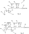
- Part of a modified pixel circuit according to a second embodiment of the invention is shown in
figure 8 . This pixel circuit is similar to the pixel circuit shown infigure 5 , except that the ANDgate 42 is replaced by acontrol circuit 60, which is described in more detail below. One advantage of this pixel circuit over the previous circuit shown infigure 5 is that it requires fewer transistors and is more compact (the AND gate being a relatively large component), thus allowing more pixels to be provided on the sensor per unit area. - The modified pixel circuit depicted in
figure 8 includes a photosensor device, a MOSFETtransistor transfer switch 18, a readout circuit and a transistor reset switch. However, for the sake of clarity only thetransfer switch 18 is shown infigure 8 , the other components of the circuit being exactly as shown infigure 5 . - The
gate terminal 40 of thetransfer switch 18 is connected to receive a control signal from thecontrol circuit 60. Thecontrol circuit 60 includes two series-connectedMOSFET control transistors select node 46 and a rowselect node 48 to receive in use a column select signal and a row select signal. Theshutter node 44 is connected to thegate terminal 40 of thetransfer switch 18 via the twocontrol transistors transfer transistor 18 when both the column select signal and the row select signal are also on. Thegate terminal 40 of thetransfer switch 18 is tied to aground connection 66 via aresistor 68, to ensure that thetransfer switch 18 remains off when no on signal is received from thecontrol circuit 60. - In operation, the
control circuit 60 provides an on control signal atoutput connection 40 only when all three input signals are on. Therefore, thetransfer switch 18 will only conduct when the shutter signal, the column select signal and the row select signal are all on. Operation of the pixel can be controlled by applying on and off signals to the columnselect node 46 and the rowselect node 48, and by applying the shutter signal to theshutter node 44. This allows each pixel in the pixel array to be activated individually, and makes it possible to capture a sequence of time-dependent lo-res image files as described above. These lo-res images can then be viewed separately in sequence or the data from all the pixels can be used to form a single hi-res image. - Part of another modified pixel circuit according to a third embodiment of the invention is shown in
figure 9 . This pixel circuit is similar to the pixel circuit shown infigure 8 , except that instead of theresistor 68, thecontrol circuit 60 includes twoadditional MOSFET transistors gate terminal 40 of thetransfer transistor 18 and theground connection 66. The gate terminals of these additional transistors are connected respectively tonodes additional transistors transfer transistor 18 in an off condition when either or both of the column select and row select signals is off. - The location of pixels in each subset does not have to follow a regular pattern as shown in
Figure 1 . An apparently random location within the pixel group can be chosen by implementing a numerical scheme, which uses a random number generator with a user supplied seed value and shuffles the location of each pixel within the pixel group. A randomized scheme has two advantages. First, the location of each pixel in the low-resolution image is randomly assigned, even though the average distance between the pixels is the same. The advantages of having randomly distributed pixels vs. a regular under-sampled array for image reconstruction is well explained in United States Patent4574311 , Random Array Sensing Devices, Resnikoff, Poggio, and Sims. Second, the low-resolution image sequence can only be recovered if the shuffled sequence of integers giving the correct timing is known. If the shuffled sequence is generated by an algorithm that incorporates a random number generating algorithm which is given a key, then the image sequence can only be recovered if the key is supplied by the person viewing the image sequence. This allows image sequences to be encrypted and protected from unauthorized viewing. - As an alternative to the rectangular geometry as shown in
Figure 1 , pixel groups can have irregular polygonal shapes. Pixel groups can therefore cover regions of interest exactly, while excluding unnecessary pixels. An example of a possible use is in the life sciences, where a user may wish to monitor the activity of a small number of cells in a microscopic field of view. The user can draw a polygonal shape around the cells of interest, and an algorithm can divide the pixels within these shapes into groups which will be exposed at different times. - If the subject imaged by the sensor was moving during the exposure time, the image may contain some "motion blur". The amount of motion blur will generally be greater than with a conventional still camera sensor in which all the pixels are exposed simultaneously, since the total integration time is greater than the exposure time of the individual pixels. However, for subjects having little or no movement, the image quality will be substantially equal to that of a conventional sensor.
- Alternatively, it may be possible to select various different image capture modes, such as a "movie/still" mode in which the pixel elements are actuated sequentially as described above, or a "still-only" mode in which all the pixel elements operate simultaneously. In movie/still mode the captured los-res images can be viewed either sequentially as a movie, or together as a hi-res still image (possibly with some motion blur). In still-only mode the motion blur will be equivalent to that of a conventional sensor, but because a set of time-separated lo-res images will not then be captured the possibility of viewing the images sequentially as a movie will not be available.
- Alternatively, a set number of pixels can be used to obtain a blur free high res. image, while the remainder can be used for obtaining a series of low res. images as previously described. The number of pixels for the high res. low blur image can be selected by the user in order to ensure the desired picture quality. For example, 50% of the pixels can be devoted to create a high resolution blur free image, where the pixels of this subgroup are distributed over the entire array. These pixels would be exposed simultaneously, for a short time equal to the optimal exposure time for a blur free image set by the user. The remaining pixels would be divided into N-1 groups as before, and exposed sequentially to generate a movie sequence. The distribution of the pixels in the high resolution group can be regular (for example, every second pixel), or the pixels can be randomly distributed, or pseudo randomly distributed (so that the average density over a defined sub area of pixels is constant, but individual pixels within that area are chosen using a known random distribution). Missing pixels in the high resolution image can be compensated for by using any of a variety of available signal processing techniques. The advantages of having randomly distributed pixels vs. a regular under-sampled array for image reconstruction is well explained in United States Patent
4574311 , Random Array Sensing Devices, Resnikoff, Poggio, and Sims. - A practical example will now be described in which the invention is implemented in a digital SLR camera having an 8.2 megapixel sensor with dimensions of 2340 x 3500 pixels. An equivalent conventional camera is currently available, which is capable of capturing full frame images at a rate of five frames per second. If the present invention were implemented in that camera it could for example capture ten 0.82 megapixel lo-res images within each full frame image. Those lo-res images could then be viewed sequentially in movie mode at a rate of fifty frames per second, and a frame size of 738 x 1108 pixels. Alternatively, data from the full set of pixels can be used to create a high resolution 8.2 megapixel still image.
- It will of course be apparent that by embedding more low resolution images within each full frame image even higher frame rates can be obtained. Alternatively, if a lower frame rate is adequate, a higher resolution movie can be captured.
- In the process described above, the interval between the successive exposures used to create the embedded lo-res images is equal to the duration of the individual exposures. The next exposure therefore starts as the previous one ends, and the total integration time Ti is equal to Nt, where N is the number of pixel subsets and t is the exposure time for the individual pixels. Alternatively, the interval between the exposures and the exposure time may be adjusted so that the exposure times overlap or are spaced apart. This would allow the user to compensate for motion blur or low light conditions. For example, instead of using exposure times of 0.25 seconds as illustrated in
Figure 2 , the exposure time may be reduced to 0.15 seconds. The exposure timings of the individual pixel subsets may be as follows:pixel subset 1 from 0 to 0.15 seconds,pixel subset 2 from 0.25 to 0.4 seconds,pixel subset 3 from 0.5 to 0.65 seconds andpixel subset 4 from 0.75 to 0.9 seconds. The total integration time will then be less than Nt. - As another example, the exposure time can be increased to 0.4 seconds, the individual exposure timings then being as follows:
pixel subset 1 from 0 to 0.4 seconds,pixel subset 2 from 0.25 to 0.65 seconds,pixel subset 3 from 0.5 to 0.9 seconds andpixel subset 4 from 0.75 to 1.15 seconds. In this case pixel subset exposures overlap (1 overlaps with 2, 2 overlaps with 3, 3 overlaps with 4 and 4 overlaps with 1). The exposure interval may therefore be optimised according to the speed at which the subject is changing or moving. - Various applications of the invention are envisaged. Some of these will now be described.
- The invention may be implemented within a camera that is intended primarily for capturing still images, to provide the possibility of capturing movies at a relatively high resolution and frame rate. For example, as indicated above, a camera that can take a sequence of 8.2 megapixel images at a rate of five frames per second would be capable of providing a movie sequence of 0.8 megapixel images at a frame rate of fifty frames per second.
- An advantage to the consumer is that the original high resolution photographs are conserved, and the data storage requirement (image size in memory) is the same as a conventional digital camera. Applications may include video acquisition and security camera operation, allowing the simultaneous capture of high resolution images for scene detail and low resolution image sequences.
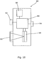
- The basic elements of a camera are illustrated schematically in
Figure 10 . Thiscamera 80 includes a lens 82 that focuses an image onto aCMOS sensor 84. Exposure of the individual pixels forming thesensor 84 to the incident light is controlled by a central processor unit (CPU) 88, which also reads data from the sensor. This data is stored in amemory device 90, for example a flash memory card. The camera includes ashutter release 92 and acontrol switch 94 that is linked to theCPU 88 and may be used to set, for example, the operational mode of the camera. The operation modes may for example include a "movie/still" mode in which the camera captures a set of time-separated lo-res images within each hi-res frame that may be viewed either as a movie or a high resolution still image, or a "still-only" mode in which the pixels are all exposed simultaneously to form a still image with minimal motion blur. The camera may also include other conventional features, such as a viewfinder, a display unit for checking settings or viewing captured images, lens controls for controlling the aperture, focal length and focussing of the lens 82, a flash unit, a data output port and so on. - Cameras that are used to monitor a changing 3D scene, which are common in surveillance applications and robotics/machine vision, must contend with several challenges. One issue is that if an object moves relative to the camera, the magnitude of movement of the image across the sensor will be inversely proportional to the distance of the object from the camera. This will cause motion blur to be more pronounced for objects close to the camera, obscuring necessary detail. For example, surveillance of a group of walking people on a street or in a building lobby would produce blurred images of their faces if they are close to the camera. Decreasing the shutter time for the whole image would potentially degrade image quality for objects far from the camera, as the total light collected from far objects will be less.
- The present invention can address this issue by varying the number of pixel groups (and hence the temporal and spatial resolution as well as total exposure time) within one frame, so as to optimise imaging of several objects within the scene. Advantageously, objects closer to the camera are proportionately larger, reducing the spatial resolution requirements and allowing for increased temporal resolution. The size of the pixel groups can be chosen using a priori knowledge of the scene (for example, vehicles monitored travelling on a highway by an elevated camera facing the direction of traffic flow would become proportionately smaller toward the top of the image, allowing the use of a gradation of pixel group sizes to maintain the average number of pixels per car). Alternatively, the size of the pixel groups can be chosen dynamically using algorithmic methods (for example, by obtaining the optical flow from motion blur in a static image, as described in Berthold and Shunck, "Determining Optical Flow", Technical Report, MIT, 1980) or range finding equipment (e.g. laser range finders or similar).
- Additionally, specific regions of interest can be imaged at different resolutions independent of the pixel group pattern used in the majority of the image. For example, a camera monitoring traffic could obtain high spatial resolution images of the licence plates of vehicles by controlling the exposure time of an appropriately chosen rectangle of pixels, while monitoring vehicle motion with low spatial resolution.
- Vehicle speed and licence plate detection could be accomplished without a radar device in such a system by using the camera to continuously monitor vehicle motion at low spatial resolution (using sufficiently large pixel groups). A computer algorithm would calculate vehicle speed and dynamically change the pixel groups to image either the whole scene or just the licence plates at high spatial resolution when required.
Claims (14)
- An image sensor having a plurality of pixels arranged in an array, selection means providing select signals for selecting individual pixels in the array, and shutter control means for transmitting a shutter signal to the pixels, wherein each said pixel includes a photosensor device, a readout circuit, a transfer switch connected between the photosensor device and the readout circuit, and a control means for triggering the pixel, characterized by the control means being connected to receive a shutter signal, a row select signal and a column select signal, and being connected to the transfer switch to control switching thereof, whereby the pixel is constructed and arranged to sense incident light only when in receipt of both a shutter signal and the select signals, whereby pixels in said array can be triggered individually to capture light at different times.
- An image sensor according to claim 1, wherein the pixels are arranged in an array of rows and columns and are connected to receive a row select signal and a column select signal, whereby an individual pixel can be selected by transmitting a row select signal and a column select signal along the row and the column in which that pixel is located.
- An image sensor according to claim 2, wherein at least one of the row select signal and the column select signal is generated by a shift register.
- An image sensor according to any one of claims 2 to 3, the control means being constructed and arranged to trigger the pixel only when it receives simultaneously a shutter signal, a row select signal and a column select signal.
- An image sensor according to claim 4, wherein the control means includes a logical AND gate having inputs for receiving a shutter signal, a row select signal and a column select signal.
- An image sensor according to claim 4, wherein the control means includes a plurality of series-connected switch devices, each switch device being operably connected to receive at least one of a shutter signal, a row select signal and a column select signal.
- An image capture device including an image sensor according to any one of the preceding claims and a data storage device for storing data from the pixels, said pixels being divided into a plurality of pixel subsets and said image capture device being constructed and arranged to capture a plurality of time-separated lo-res images, each said lo-res image comprising the data from a different pixel subset.
- An image capture device according to claim 7, including a control device for controlling operation of the pixel array, wherein the control device is constructed and arranged to trigger the pixels in a predefined, random or pseudo-random sequence.
- A camera including an image capture device according to claim 7 or claim 8.
- A method of capturing images using an image sensor having a plurality of pixels arranged in an array, the method comprising:providing select signals for selecting individual pixels in the array using selection means, andtransmitting a shutter signal to the pixels using shutter control means,wherein each said pixel includes a photosensor device, a readout circuit, a transfer switch connected between the photosensor device and the readout circuit, andtriggering the pixel using control means, characterised by receiving by the control means a shutter signal, a row select signal and a column select signal, andcontrolling by the control means switching of the transfer switch,whereby the pixel senses incident light only when in receipt of both a shutter signal and the select signals,whereby said pixels are triggered individually to capture light at different times.
- A method according to claim 10, wherein the pixels are arranged in an array of rows and columns and an individual pixel is selected by transmitting a row select signal and a column select signal along the row and the column in which that pixel is located.
- A method according to claim 11, wherein at least one of the row select signal and the column select signal is generated by a shift register.
- A method according to claim 11 or claim 12, wherein each pixel is triggered to sense incident light only when it receives simultaneously a shutter signal, a row select signal and a column select signal.
- A method according to any one of claims 10 to 13, including capturing a plurality of time-separated lo-res images, each lo-res image comprising the data from a different one of a plurality of pixel subsets.
Applications Claiming Priority (2)
| Application Number | Priority Date | Filing Date | Title |
|---|---|---|---|
| GBGB1012631.6A GB201012631D0 (en) | 2010-07-28 | 2010-07-28 | Image sensor and method of sensing |
| PCT/GB2011/001051 WO2012013918A1 (en) | 2010-07-28 | 2011-07-12 | Image sensor and method of sensing |
Publications (2)
| Publication Number | Publication Date |
|---|---|
| EP2599300A1 EP2599300A1 (en) | 2013-06-05 |
| EP2599300B1 true EP2599300B1 (en) | 2020-02-19 |
Family
ID=42799205
Family Applications (1)
| Application Number | Title | Priority Date | Filing Date |
|---|---|---|---|
| EP11739130.0A Active EP2599300B1 (en) | 2010-07-28 | 2011-07-12 | Image sensor and method of sensing |
Country Status (5)
| Country | Link |
|---|---|
| US (1) | US9247167B2 (en) |
| EP (1) | EP2599300B1 (en) |
| JP (1) | JP5944387B2 (en) |
| GB (1) | GB201012631D0 (en) |
| WO (1) | WO2012013918A1 (en) |
Families Citing this family (8)
| Publication number | Priority date | Publication date | Assignee | Title |
|---|---|---|---|---|
| US8786732B2 (en) | 2012-10-31 | 2014-07-22 | Pixon Imaging, Inc. | Device and method for extending dynamic range in an image sensor |
| US20140168415A1 (en) * | 2012-12-07 | 2014-06-19 | Magna Electronics Inc. | Vehicle vision system with micro lens array |
| CN106134181B (en) * | 2014-03-24 | 2019-03-01 | 富士胶片株式会社 | Camera |
| US9819841B1 (en) * | 2015-04-17 | 2017-11-14 | Altera Corporation | Integrated circuits with optical flow computation circuitry |
| JP7042025B2 (en) * | 2017-01-23 | 2022-03-25 | ソニーセミコンダクタソリューションズ株式会社 | Information processing equipment, information processing method, and recording medium |
| GB2574619B (en) | 2018-06-12 | 2022-10-12 | Res & Innovation Uk | Image sensor |
| EP3614174B1 (en) * | 2018-08-21 | 2021-06-23 | Omron Corporation | Distance measuring device and distance measuring method |
| EP4235219A1 (en) | 2022-02-28 | 2023-08-30 | Imasenic Advanced Imaging, S.L. | Depth scanning image sensor |
Citations (1)
| Publication number | Priority date | Publication date | Assignee | Title |
|---|---|---|---|---|
| JP2006121151A (en) * | 2004-10-19 | 2006-05-11 | Sony Corp | Signal processing method, signal processing apparatus and physical information acquiring apparatus |
Family Cites Families (31)
| Publication number | Priority date | Publication date | Assignee | Title |
|---|---|---|---|---|
| US4574311A (en) | 1985-04-04 | 1986-03-04 | Thinking Machines Corporation | Random array sensing devices |
| KR100228424B1 (en) * | 1996-06-29 | 1999-11-01 | 김영환 | X-decoder circuit of semiconductor memory device |
| AU5457098A (en) * | 1997-08-15 | 1999-03-08 | Intel Corporation | Color channel independent electronic shutter for solid state image sensor |
| US6369853B1 (en) * | 1997-11-13 | 2002-04-09 | Foveon, Inc. | Intra-pixel frame storage element, array, and electronic shutter method suitable for electronic still camera applications |
| DE19928454B4 (en) * | 1998-06-29 | 2010-01-21 | Fujitsu Microelectronics Ltd. | Memory device with row decoder |
| JP3581953B2 (en) * | 1999-07-26 | 2004-10-27 | 沖電気工業株式会社 | Semiconductor storage device |
| JP3942332B2 (en) * | 2000-01-07 | 2007-07-11 | 富士通株式会社 | Semiconductor memory device |
| KR100359770B1 (en) * | 2000-03-02 | 2002-11-04 | 주식회사 하이닉스반도체 | Active pixel circuit in CMOS image sensor |
| US7268815B1 (en) * | 2000-10-06 | 2007-09-11 | Cypress Semiconductor Corporation (Belgium) Bvba | Differential readout of a pixel array with elimination of pixel- and column-wise fixed pattern noise |
| JP4356231B2 (en) * | 2000-11-21 | 2009-11-04 | コニカミノルタホールディングス株式会社 | Scanning circuit and imaging apparatus including the same |
| US6720592B1 (en) * | 2001-06-29 | 2004-04-13 | National Semiconductor Corp. | Apparatus for high sensitivity, low lag, high voltage swing in a pixel cell with an electronic shutter |
| US7106377B2 (en) * | 2001-07-25 | 2006-09-12 | Hewlett-Packard Development Company, L.P. | Image capturing device capable of single pixel exposure duration control |
| US7499091B2 (en) * | 2002-03-20 | 2009-03-03 | Sony Corporation | Solid-state imaging device and method for driving same |
| ITUD20020084A1 (en) * | 2002-04-12 | 2003-10-13 | Neuricam Spa | ELECTRONIC SELECTOR DEVICE FOR ELECTRO-OPTICAL SENSORS |
| KR100562489B1 (en) * | 2002-11-11 | 2006-03-21 | 삼성전자주식회사 | CMOS image sensor having row decoder capable of shutter timing control |
| JP4687155B2 (en) * | 2005-03-09 | 2011-05-25 | ソニー株式会社 | Solid-state imaging device and driving method thereof |
| JP2007166238A (en) * | 2005-12-14 | 2007-06-28 | Victor Co Of Japan Ltd | Cmos sensor with shutter function per pixel |
| JP2008271186A (en) * | 2007-04-20 | 2008-11-06 | Olympus Corp | Solid-state imaging apparatus |
| GB0709026D0 (en) * | 2007-05-10 | 2007-06-20 | Isis Innovation | High speed imaging with slow scan cameras using pixel level dynami shuttering |
| JP5022108B2 (en) * | 2007-06-01 | 2012-09-12 | ルネサスエレクトロニクス株式会社 | Semiconductor memory device and test method thereof |
| DE102007045448A1 (en) * | 2007-09-24 | 2009-04-02 | Arnold & Richter Cine Technik Gmbh & Co. Betriebs Kg | image sensor |
| JP4442675B2 (en) * | 2007-09-28 | 2010-03-31 | ソニー株式会社 | Pixel drive circuit, imaging device, and camera system |
| JP2009253559A (en) * | 2008-04-03 | 2009-10-29 | Sharp Corp | Solid-state imaging device and electronics information device |
| JP2009296477A (en) * | 2008-06-09 | 2009-12-17 | Olympus Corp | Solid-state imaging apparatus |
| US7889256B2 (en) * | 2008-06-11 | 2011-02-15 | Aptina Imaging Corporation | Method and apparatus for reducing temporal row-wise noise in imagers |
| JP5446282B2 (en) * | 2009-01-21 | 2014-03-19 | ソニー株式会社 | Solid-state imaging device and camera system |
| JP5661260B2 (en) * | 2009-07-16 | 2015-01-28 | キヤノン株式会社 | Solid-state imaging device and driving method thereof |
| JP5598126B2 (en) * | 2010-07-09 | 2014-10-01 | ソニー株式会社 | Solid-state imaging device and camera system |
| JP5999402B2 (en) * | 2011-08-12 | 2016-09-28 | ソニー株式会社 | Solid-state imaging device, manufacturing method, and electronic apparatus |
| US20130140442A1 (en) * | 2011-12-02 | 2013-06-06 | Sony Corporation | Amplifying circuit and manufacturing method, solid-state imaging element, and electronic device |
| JP2014187270A (en) * | 2013-03-25 | 2014-10-02 | Sony Corp | Solid state image sensor and manufacturing method therefor, and electronic apparatus |
-
2010
- 2010-07-28 GB GBGB1012631.6A patent/GB201012631D0/en not_active Ceased
-
2011
- 2011-07-12 EP EP11739130.0A patent/EP2599300B1/en active Active
- 2011-07-12 WO PCT/GB2011/001051 patent/WO2012013918A1/en active Application Filing
- 2011-07-12 JP JP2013521202A patent/JP5944387B2/en active Active
- 2011-07-12 US US13/811,724 patent/US9247167B2/en active Active
Patent Citations (1)
| Publication number | Priority date | Publication date | Assignee | Title |
|---|---|---|---|---|
| JP2006121151A (en) * | 2004-10-19 | 2006-05-11 | Sony Corp | Signal processing method, signal processing apparatus and physical information acquiring apparatus |
Also Published As
| Publication number | Publication date |
|---|---|
| EP2599300A1 (en) | 2013-06-05 |
| JP5944387B2 (en) | 2016-07-05 |
| US9247167B2 (en) | 2016-01-26 |
| US20130182160A1 (en) | 2013-07-18 |
| WO2012013918A1 (en) | 2012-02-02 |
| WO2012013918A4 (en) | 2012-03-08 |
| JP2013536625A (en) | 2013-09-19 |
| GB201012631D0 (en) | 2010-09-15 |
Similar Documents
| Publication | Publication Date | Title |
|---|---|---|
| EP2599300B1 (en) | Image sensor and method of sensing | |
| EP2145467B1 (en) | Image capture device and method | |
| US11050955B2 (en) | Solid-state imaging device, method for driving solid-state imaging device, and electronic apparatus | |
| KR102632643B1 (en) | Image sensor and electronic device | |
| US9438868B2 (en) | Adaptive image sensor systems and methods | |
| WO2013043259A1 (en) | Imaging system with foveated imaging capabilities | |
| EP2478558A1 (en) | Image sensor with wide dynamic range | |
| EP3378224A1 (en) | Image sensor system | |
| JP2013536625A5 (en) | ||
| KR20030029124A (en) | All-eletronic high-resolution digital still camera | |
| US9282245B2 (en) | Image capturing apparatus and method of controlling the same | |
| JP7433792B2 (en) | Imaging device and its control method | |
| JP2019103121A (en) | Imaging device, imaging apparatus, and imaging method | |
| JP2020028115A (en) | Imaging apparatus | |
| JP2017194280A (en) | Imaging circuit, signal readout circuit, infrared imaging device, infrared detection circuit and operation method of imaging circuit | |
| WO2019216029A1 (en) | Imaging device, electronic apparatus, and drive method | |
| JP2005303546A (en) | Imaging apparatus and driving method thereof | |
| WO2013030561A1 (en) | Pixel circuit |
Legal Events
| Date | Code | Title | Description |
|---|---|---|---|
| PUAI | Public reference made under article 153(3) epc to a published international application that has entered the european phase |
Free format text: ORIGINAL CODE: 0009012 |
|
| 17P | Request for examination filed |
Effective date: 20130125 |
|
| AK | Designated contracting states |
Kind code of ref document: A1 Designated state(s): AL AT BE BG CH CY CZ DE DK EE ES FI FR GB GR HR HU IE IS IT LI LT LU LV MC MK MT NL NO PL PT RO RS SE SI SK SM TR |
|
| DAX | Request for extension of the european patent (deleted) | ||
| RAP1 | Party data changed (applicant data changed or rights of an application transferred) |
Owner name: OXFORD UNIVERSITY INNOVATION LIMITED |
|
| RAP1 | Party data changed (applicant data changed or rights of an application transferred) |
Owner name: OXFORD UNIVERSITY INNOVATION LIMITED |
|
| STAA | Information on the status of an ep patent application or granted ep patent |
Free format text: STATUS: EXAMINATION IS IN PROGRESS |
|
| 17Q | First examination report despatched |
Effective date: 20170508 |
|
| REG | Reference to a national code |
Ref country code: DE Ref legal event code: R079 Ref document number: 602011065085 Country of ref document: DE Free format text: PREVIOUS MAIN CLASS: H04N0005232000 Ipc: H04N0005345000 |
|
| GRAP | Despatch of communication of intention to grant a patent |
Free format text: ORIGINAL CODE: EPIDOSNIGR1 |
|
| STAA | Information on the status of an ep patent application or granted ep patent |
Free format text: STATUS: GRANT OF PATENT IS INTENDED |
|
| RIC1 | Information provided on ipc code assigned before grant |
Ipc: H04N 5/343 20110101ALI20190819BHEP Ipc: H04N 5/345 20110101AFI20190819BHEP Ipc: H04N 5/3745 20110101ALI20190819BHEP Ipc: H04N 5/353 20110101ALI20190819BHEP |
|
| INTG | Intention to grant announced |
Effective date: 20190919 |
|
| GRAS | Grant fee paid |
Free format text: ORIGINAL CODE: EPIDOSNIGR3 |
|
| GRAA | (expected) grant |
Free format text: ORIGINAL CODE: 0009210 |
|
| STAA | Information on the status of an ep patent application or granted ep patent |
Free format text: STATUS: THE PATENT HAS BEEN GRANTED |
|
| AK | Designated contracting states |
Kind code of ref document: B1 Designated state(s): AL AT BE BG CH CY CZ DE DK EE ES FI FR GB GR HR HU IE IS IT LI LT LU LV MC MK MT NL NO PL PT RO RS SE SI SK SM TR |
|
| REG | Reference to a national code |
Ref country code: GB Ref legal event code: FG4D |
|
| REG | Reference to a national code |
Ref country code: CH Ref legal event code: EP |
|
| REG | Reference to a national code |
Ref country code: DE Ref legal event code: R096 Ref document number: 602011065085 Country of ref document: DE |
|
| REG | Reference to a national code |
Ref country code: AT Ref legal event code: REF Ref document number: 1236307 Country of ref document: AT Kind code of ref document: T Effective date: 20200315 |
|
| REG | Reference to a national code |
Ref country code: IE Ref legal event code: FG4D |
|
| REG | Reference to a national code |
Ref country code: NL Ref legal event code: FP |
|
| PG25 | Lapsed in a contracting state [announced via postgrant information from national office to epo] |
Ref country code: FI Free format text: LAPSE BECAUSE OF FAILURE TO SUBMIT A TRANSLATION OF THE DESCRIPTION OR TO PAY THE FEE WITHIN THE PRESCRIBED TIME-LIMIT Effective date: 20200219 Ref country code: NO Free format text: LAPSE BECAUSE OF FAILURE TO SUBMIT A TRANSLATION OF THE DESCRIPTION OR TO PAY THE FEE WITHIN THE PRESCRIBED TIME-LIMIT Effective date: 20200519 Ref country code: RS Free format text: LAPSE BECAUSE OF FAILURE TO SUBMIT A TRANSLATION OF THE DESCRIPTION OR TO PAY THE FEE WITHIN THE PRESCRIBED TIME-LIMIT Effective date: 20200219 |
|
| REG | Reference to a national code |
Ref country code: LT Ref legal event code: MG4D |
|
| PG25 | Lapsed in a contracting state [announced via postgrant information from national office to epo] |
Ref country code: IS Free format text: LAPSE BECAUSE OF FAILURE TO SUBMIT A TRANSLATION OF THE DESCRIPTION OR TO PAY THE FEE WITHIN THE PRESCRIBED TIME-LIMIT Effective date: 20200619 Ref country code: GR Free format text: LAPSE BECAUSE OF FAILURE TO SUBMIT A TRANSLATION OF THE DESCRIPTION OR TO PAY THE FEE WITHIN THE PRESCRIBED TIME-LIMIT Effective date: 20200520 Ref country code: BG Free format text: LAPSE BECAUSE OF FAILURE TO SUBMIT A TRANSLATION OF THE DESCRIPTION OR TO PAY THE FEE WITHIN THE PRESCRIBED TIME-LIMIT Effective date: 20200519 Ref country code: SE Free format text: LAPSE BECAUSE OF FAILURE TO SUBMIT A TRANSLATION OF THE DESCRIPTION OR TO PAY THE FEE WITHIN THE PRESCRIBED TIME-LIMIT Effective date: 20200219 Ref country code: LV Free format text: LAPSE BECAUSE OF FAILURE TO SUBMIT A TRANSLATION OF THE DESCRIPTION OR TO PAY THE FEE WITHIN THE PRESCRIBED TIME-LIMIT Effective date: 20200219 Ref country code: HR Free format text: LAPSE BECAUSE OF FAILURE TO SUBMIT A TRANSLATION OF THE DESCRIPTION OR TO PAY THE FEE WITHIN THE PRESCRIBED TIME-LIMIT Effective date: 20200219 |
|
| PG25 | Lapsed in a contracting state [announced via postgrant information from national office to epo] |
Ref country code: ES Free format text: LAPSE BECAUSE OF FAILURE TO SUBMIT A TRANSLATION OF THE DESCRIPTION OR TO PAY THE FEE WITHIN THE PRESCRIBED TIME-LIMIT Effective date: 20200219 Ref country code: DK Free format text: LAPSE BECAUSE OF FAILURE TO SUBMIT A TRANSLATION OF THE DESCRIPTION OR TO PAY THE FEE WITHIN THE PRESCRIBED TIME-LIMIT Effective date: 20200219 Ref country code: SK Free format text: LAPSE BECAUSE OF FAILURE TO SUBMIT A TRANSLATION OF THE DESCRIPTION OR TO PAY THE FEE WITHIN THE PRESCRIBED TIME-LIMIT Effective date: 20200219 Ref country code: RO Free format text: LAPSE BECAUSE OF FAILURE TO SUBMIT A TRANSLATION OF THE DESCRIPTION OR TO PAY THE FEE WITHIN THE PRESCRIBED TIME-LIMIT Effective date: 20200219 Ref country code: PT Free format text: LAPSE BECAUSE OF FAILURE TO SUBMIT A TRANSLATION OF THE DESCRIPTION OR TO PAY THE FEE WITHIN THE PRESCRIBED TIME-LIMIT Effective date: 20200712 Ref country code: LT Free format text: LAPSE BECAUSE OF FAILURE TO SUBMIT A TRANSLATION OF THE DESCRIPTION OR TO PAY THE FEE WITHIN THE PRESCRIBED TIME-LIMIT Effective date: 20200219 Ref country code: EE Free format text: LAPSE BECAUSE OF FAILURE TO SUBMIT A TRANSLATION OF THE DESCRIPTION OR TO PAY THE FEE WITHIN THE PRESCRIBED TIME-LIMIT Effective date: 20200219 Ref country code: SM Free format text: LAPSE BECAUSE OF FAILURE TO SUBMIT A TRANSLATION OF THE DESCRIPTION OR TO PAY THE FEE WITHIN THE PRESCRIBED TIME-LIMIT Effective date: 20200219 Ref country code: CZ Free format text: LAPSE BECAUSE OF FAILURE TO SUBMIT A TRANSLATION OF THE DESCRIPTION OR TO PAY THE FEE WITHIN THE PRESCRIBED TIME-LIMIT Effective date: 20200219 |
|
| REG | Reference to a national code |
Ref country code: AT Ref legal event code: MK05 Ref document number: 1236307 Country of ref document: AT Kind code of ref document: T Effective date: 20200219 |
|
| REG | Reference to a national code |
Ref country code: DE Ref legal event code: R097 Ref document number: 602011065085 Country of ref document: DE |
|
| PLBE | No opposition filed within time limit |
Free format text: ORIGINAL CODE: 0009261 |
|
| STAA | Information on the status of an ep patent application or granted ep patent |
Free format text: STATUS: NO OPPOSITION FILED WITHIN TIME LIMIT |
|
| 26N | No opposition filed |
Effective date: 20201120 |
|
| PG25 | Lapsed in a contracting state [announced via postgrant information from national office to epo] |
Ref country code: IT Free format text: LAPSE BECAUSE OF FAILURE TO SUBMIT A TRANSLATION OF THE DESCRIPTION OR TO PAY THE FEE WITHIN THE PRESCRIBED TIME-LIMIT Effective date: 20200219 Ref country code: AT Free format text: LAPSE BECAUSE OF FAILURE TO SUBMIT A TRANSLATION OF THE DESCRIPTION OR TO PAY THE FEE WITHIN THE PRESCRIBED TIME-LIMIT Effective date: 20200219 |
|
| PG25 | Lapsed in a contracting state [announced via postgrant information from national office to epo] |
Ref country code: SI Free format text: LAPSE BECAUSE OF FAILURE TO SUBMIT A TRANSLATION OF THE DESCRIPTION OR TO PAY THE FEE WITHIN THE PRESCRIBED TIME-LIMIT Effective date: 20200219 Ref country code: PL Free format text: LAPSE BECAUSE OF FAILURE TO SUBMIT A TRANSLATION OF THE DESCRIPTION OR TO PAY THE FEE WITHIN THE PRESCRIBED TIME-LIMIT Effective date: 20200219 Ref country code: MC Free format text: LAPSE BECAUSE OF FAILURE TO SUBMIT A TRANSLATION OF THE DESCRIPTION OR TO PAY THE FEE WITHIN THE PRESCRIBED TIME-LIMIT Effective date: 20200219 |
|
| REG | Reference to a national code |
Ref country code: CH Ref legal event code: PL |
|
| REG | Reference to a national code |
Ref country code: BE Ref legal event code: MM Effective date: 20200731 |
|
| PG25 | Lapsed in a contracting state [announced via postgrant information from national office to epo] |
Ref country code: CH Free format text: LAPSE BECAUSE OF NON-PAYMENT OF DUE FEES Effective date: 20200731 Ref country code: LI Free format text: LAPSE BECAUSE OF NON-PAYMENT OF DUE FEES Effective date: 20200731 Ref country code: LU Free format text: LAPSE BECAUSE OF NON-PAYMENT OF DUE FEES Effective date: 20200712 |
|
| PG25 | Lapsed in a contracting state [announced via postgrant information from national office to epo] |
Ref country code: BE Free format text: LAPSE BECAUSE OF NON-PAYMENT OF DUE FEES Effective date: 20200731 |
|
| PG25 | Lapsed in a contracting state [announced via postgrant information from national office to epo] |
Ref country code: IE Free format text: LAPSE BECAUSE OF NON-PAYMENT OF DUE FEES Effective date: 20200712 |
|
| PG25 | Lapsed in a contracting state [announced via postgrant information from national office to epo] |
Ref country code: TR Free format text: LAPSE BECAUSE OF FAILURE TO SUBMIT A TRANSLATION OF THE DESCRIPTION OR TO PAY THE FEE WITHIN THE PRESCRIBED TIME-LIMIT Effective date: 20200219 Ref country code: MT Free format text: LAPSE BECAUSE OF FAILURE TO SUBMIT A TRANSLATION OF THE DESCRIPTION OR TO PAY THE FEE WITHIN THE PRESCRIBED TIME-LIMIT Effective date: 20200219 Ref country code: CY Free format text: LAPSE BECAUSE OF FAILURE TO SUBMIT A TRANSLATION OF THE DESCRIPTION OR TO PAY THE FEE WITHIN THE PRESCRIBED TIME-LIMIT Effective date: 20200219 |
|
| PG25 | Lapsed in a contracting state [announced via postgrant information from national office to epo] |
Ref country code: MK Free format text: LAPSE BECAUSE OF FAILURE TO SUBMIT A TRANSLATION OF THE DESCRIPTION OR TO PAY THE FEE WITHIN THE PRESCRIBED TIME-LIMIT Effective date: 20200219 Ref country code: AL Free format text: LAPSE BECAUSE OF FAILURE TO SUBMIT A TRANSLATION OF THE DESCRIPTION OR TO PAY THE FEE WITHIN THE PRESCRIBED TIME-LIMIT Effective date: 20200219 |
|
| REG | Reference to a national code |
Ref country code: DE Ref legal event code: R079 Ref document number: 602011065085 Country of ref document: DE Free format text: PREVIOUS MAIN CLASS: H04N0005345000 Ipc: H04N0025440000 |
|
| P01 | Opt-out of the competence of the unified patent court (upc) registered |
Effective date: 20230525 |
|
| PGFP | Annual fee paid to national office [announced via postgrant information from national office to epo] |
Ref country code: NL Payment date: 20230704 Year of fee payment: 13 |
|
| PGFP | Annual fee paid to national office [announced via postgrant information from national office to epo] |
Ref country code: GB Payment date: 20230718 Year of fee payment: 13 |
|
| PGFP | Annual fee paid to national office [announced via postgrant information from national office to epo] |
Ref country code: FR Payment date: 20230718 Year of fee payment: 13 Ref country code: DE Payment date: 20230704 Year of fee payment: 13 |