JP2006121151A - Signal processing method, signal processing apparatus and physical information acquiring apparatus - Google Patents
Signal processing method, signal processing apparatus and physical information acquiring apparatus Download PDFInfo
- Publication number
- JP2006121151A JP2006121151A JP2004303922A JP2004303922A JP2006121151A JP 2006121151 A JP2006121151 A JP 2006121151A JP 2004303922 A JP2004303922 A JP 2004303922A JP 2004303922 A JP2004303922 A JP 2004303922A JP 2006121151 A JP2006121151 A JP 2006121151A
- Authority
- JP
- Japan
- Prior art keywords
- unit
- detection
- signal
- signal processing
- physical quantity
- Prior art date
- Legal status (The legal status is an assumption and is not a legal conclusion. Google has not performed a legal analysis and makes no representation as to the accuracy of the status listed.)
- Pending
Links
Images


Abstract
Description
本発明は、信号処理方法および信号処理装置並びに物理情報取得装置に関する。より詳細には、たとえば光や放射線などの外部から入力される電磁波に対して感応性をする複数の単位構成要素が配列されてなり、単位構成要素により電気信号に変換された物理量分布を、アドレス制御により任意選択して電気信号として読出可能な、たとえば固体撮像装置などの、物理量分布検知の装置に用いて好適な、信号を読み出して所定目的用の情報を取得する際の信号処理技術に関する。たとえば、AGC、WB、γ補正の各信号処理技術に関する。 The present invention relates to a signal processing method, a signal processing device, and a physical information acquisition device. More specifically, for example, a plurality of unit components that are sensitive to electromagnetic waves input from outside such as light and radiation are arranged, and the physical quantity distribution converted into an electric signal by the unit components is addressed. The present invention relates to a signal processing technique for reading out a signal and acquiring information for a predetermined purpose, which is suitable for use in a physical quantity distribution detection device such as a solid-state imaging device that can be arbitrarily selected by control and read out as an electrical signal. For example, the present invention relates to signal processing techniques for AGC, WB, and γ correction.
光や放射線などの外部から入力される電磁波あるいは圧力(接触など)などの物理量変化に対して感応性をする単位構成要素(たとえば画素)をライン状もしくはマトリクス状に複数個配列してなる物理量分布検知半導体装置が様々な分野で使われている。 Physical quantity distribution formed by arranging multiple unit components (for example, pixels) that are sensitive to changes in physical quantity such as electromagnetic waves or pressure (contact, etc.) input from outside such as light and radiation, in a line or matrix form. Sensing semiconductor devices are used in various fields.
たとえば、映像機器の分野では、物理量の一例である光(電磁波の一例)の変化を検出するCCD(Charge Coupled Device )型あるいはMOS(Metal Oxide Semiconductor )やCMOS(Complementary Metal-oxide Semiconductor )型の撮像素子(撮像デバイス)を用いた固体撮像装置が使われている。ここで“固体”とは半導体製であることを意味している。 For example, in the field of video equipment, CCD (Charge Coupled Device) type or MOS (Metal Oxide Semiconductor) type or CMOS (Complementary Metal-oxide Semiconductor) type imaging that detects changes in light (an example of electromagnetic waves) which is an example of physical quantity. A solid-state imaging device using an element (imaging device) is used. Here, “solid” means made of semiconductor.
たとえばCCDやCMOSイメージセンサに代表される固体撮像素子の小型化、低価格化により、これらを利用した各種映像機器、たとえば静止画を撮影するデジタルスチルカメラやカメラ付き携帯電話あるいは動画を撮影するビデオカメラなどが急激に普及しつつある。なかでもCMOSイメージセンサは、CCDに比べて低消費電力、低コストで製造可能であることから、将来CCDを置き換えるものとして注目を集めている。 For example, by reducing the size and price of solid-state image sensors represented by CCDs and CMOS image sensors, various video devices using them, such as digital still cameras for taking still pictures, mobile phones with cameras, or videos for taking moving pictures Cameras etc. are spreading rapidly. In particular, CMOS image sensors are attracting attention as a replacement for CCDs in the future because they can be manufactured with lower power consumption and lower cost than CCDs.
また、近年、半導体技術の進歩により、固体撮像素子の高画素化が急速に進んでおり、たとえば数100万画素の固体撮像素子が開発され、高解像度が要求されるデジタルスチルカメラや映画用のビデオカメラなどに利用されている。その中でもCMOSセンサは各画素に光電変換素子と読出回路が設けられた固体撮像装置であり、各画素をランダムにアクセスすることや高速に読み出すことができることから、将来を有望視されているセンサである。 In recent years, with the advancement of semiconductor technology, the number of pixels of solid-state image sensors has been rapidly increasing. For example, solid-state image sensors having several million pixels have been developed and used for digital still cameras and movies for which high resolution is required. Used for video cameras. Among them, the CMOS sensor is a solid-state imaging device in which each pixel is provided with a photoelectric conversion element and a readout circuit. Since each pixel can be accessed at random or read out at high speed, it is a promising sensor for the future. is there.
また、コンピュータ機器の分野では、指紋に関する情報を圧力に基づく電気的特性の変化や光学的特性の変化に基づき指紋の像を検出する指紋認証装置などが使われている。これらは、単位構成要素(固体撮像装置にあっては画素)によって電気信号に変換された物理量分布を電気信号として読み出す。 In the field of computer equipment, fingerprint authentication devices that detect fingerprint images based on changes in electrical characteristics and optical characteristics based on pressure are used. These read out, as an electrical signal, a physical quantity distribution converted into an electrical signal by a unit component (a pixel in a solid-state imaging device).
一方、固体撮像装置の中には、電荷生成部で生成された信号電荷に応じた画素信号を生成する画素信号生成部に静電誘導トランジスタやMOSトランジスタなどの増幅用の駆動トランジスタを有する増幅型固体撮像素子(APS;Active Pixel Sensor /ゲインセルともいわれる)構成の画素を備えた増幅型固体撮像装置がある。たとえば、CMOS型固体撮像装置の多くはそのような構成をなしている。 On the other hand, some solid-state imaging devices have an amplification driving transistor such as an electrostatic induction transistor or a MOS transistor in a pixel signal generation unit that generates a pixel signal corresponding to the signal charge generated in the charge generation unit. There is an amplifying solid-state imaging device including a pixel having a solid-state imaging device (APS: Active Pixel Sensor / gain cell) configuration. For example, many CMOS solid-state imaging devices have such a configuration.
このような増幅型固体撮像装置において画素信号を外部に読み出すには、複数の単位画素が配列されている撮像部(画素部ともいう)に対してアドレス制御をし、個々の単位画素からの信号を任意に選択して読み出すようにしている。つまり、増幅型固体撮像装置は、アドレス制御型の固体撮像装置の一例である。 In such an amplification type solid-state imaging device, in order to read out pixel signals to the outside, address control is performed on an imaging unit (also referred to as a pixel unit) in which a plurality of unit pixels are arranged, and signals from individual unit pixels are transmitted. Is arbitrarily selected and read out. That is, the amplification type solid-state imaging device is an example of an address control type solid-state imaging device.
たとえば、単位画素がマトリクス状に配されたX−Yアドレス型固体撮像素子の一種である増幅型固体撮像素子は、画素そのものに増幅機能を持たせるために、MOS構造などの能動素子(MOSトランジスタ)を用いて画素を構成している。すなわち、光電変換素子であるフォトダイオードに蓄積された信号電荷(光電子)を前記能動素子で増幅し、画像情報として読み出す。 For example, an amplification type solid-state imaging device which is a kind of XY address type solid-state imaging device in which unit pixels are arranged in a matrix form an active element (MOS transistor) such as a MOS structure in order to give the pixel itself an amplification function. ) To form a pixel. That is, signal charges (photoelectrons) accumulated in a photodiode which is a photoelectric conversion element are amplified by the active element and read out as image information.
この種のX−Yアドレス型固体撮像素子では、たとえば、画素トランジスタが2次元行列状に多数配列されて撮像部が構成され、ライン(行)ごとあるいは画素ごとに入射光に対応する信号電荷の蓄積が開始され、その蓄積された信号電荷に基づく電流または電圧の信号がアドレス指定によって各画素から所定順に読み出される。 In this type of XY address type solid-state imaging device, for example, a large number of pixel transistors are arranged in a two-dimensional matrix to form an imaging unit, and a signal charge corresponding to incident light for each line (row) or each pixel. Accumulation is started, and a current or voltage signal based on the accumulated signal charge is read from each pixel in a predetermined order by addressing.
ここで、MOS(CMOSを含む)型においては、アドレス制御の一例として、1行分を同時にアクセスして行単位で画素信号を撮像部から読み出し、必要に応じて所定の信号処理を施し、その後に、各行の1行分の画素信号を順次出力側に読み出す方式が多く用いられている。たとえばマトリクス状に配置された画素の信号出力が行ごとに順次垂直信号線に送られ、垂直信号線からさらに水平方向に順次水平読出線に接続されて出力される。 Here, in the MOS (including CMOS) type, as an example of address control, one row is accessed simultaneously, pixel signals are read out from the imaging unit in units of rows, and predetermined signal processing is performed as necessary. In addition, a method of sequentially reading out pixel signals for one row of each row to the output side is often used. For example, the signal output of the pixels arranged in a matrix is sequentially sent to the vertical signal line for each row, and is further connected from the vertical signal line to the horizontal readout line in the horizontal direction.
また、撮像部から読み出されたアナログの画素信号は、必要に応じて、アナログ−デジタル変換装置(AD変換装置;Analog Digital Converter)にてデジタルデータに変換する。 The analog pixel signal read from the imaging unit is converted into digital data by an analog-digital converter (AD converter; Analog Digital Converter) as necessary.
また、CCD(Charge Coupled Device) 撮像素子やCMOS(Complementary Metal-Oxide Semiconductor )撮像素子などの撮像素子(撮像デバイス)を用いて画像を撮像する撮像装置においては、デジタル画像信号処理LSI(Large Scale Integrated Circuit;大規模集積回路)との組合せを利用して、画像データに対する電子的な処理によって、カメラの機能を電子部品を中心に構成することが可能である。 In an imaging apparatus that captures an image using an imaging element (imaging device) such as a CCD (Charge Coupled Device) imaging element or a CMOS (Complementary Metal-Oxide Semiconductor) imaging element, a digital image signal processing LSI (Large Scale Integrated) is used. The function of the camera can be configured around electronic components by electronic processing on image data using a combination with a circuit (large-scale integrated circuit).
たとえば、補色の撮像データから、赤(R),緑(G),青(B)の原色信号を分離・同時化する原色分離処理、ホワイトバランス(WB;White Balance )をとるホワイトバランス調整処理、周辺画素のデータを用いて画素を補う画素補間処理、階調度合いを調整するガンマ(γ)補正処理、あるいは色差マトリクス処理やエンコード処理を行なって輝度データ(Y)や色データ(C)(纏めてデジタル映像データともいう)を生成するYC信号生成処理などを行なう(たとえば非特許文献1参照)。 For example, primary color separation processing that separates and synchronizes primary color signals of red (R), green (G), and blue (B) from complementary color imaging data, white balance adjustment processing that takes white balance (WB), Luminance data (Y) and color data (C) (summary) are obtained by performing pixel interpolation processing that supplements pixels using peripheral pixel data, gamma (γ) correction processing that adjusts the degree of gradation, or color difference matrix processing and encoding processing. YC signal generation processing for generating digital video data) (see, for example, Non-Patent Document 1).
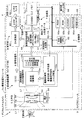
図12は、ホワイトバランス調整処理、画素補間処理、およびガンマ補正処理などの機能を実現する仕組みを持つ従来の撮像装置の構成例を説明する図である。 FIG. 12 is a diagram illustrating a configuration example of a conventional imaging apparatus having a mechanism for realizing functions such as white balance adjustment processing, pixel interpolation processing, and gamma correction processing.
図12に示すように、固体撮像素子910は、タイミング制御部991からの駆動パルスにしたがって動作するようになっている。また、全体の信号号処理系は、固体撮像素子910からのアナログ撮像信号をサンプリングすることによってノイズを低減させるCDS(Correlated Double Sampling:相関2重サンプリング)回路962aや、CDS処理された画素信号を増幅するAGC(Automatic Gain Control;自動利得制御)機能を持った増幅アンプ962bなどを有するプリアンプ部962、プリアンプ部962が出力するアナログ信号をデジタル信号に変換するAD(Analog/Digital)変換部964を備えた前段の信号処理系統960aを備えて構成されている。さらにAD変換部964から入力されるデジタル信号に所定の画像処理を施す後段の信号処理系統960bを備えて構成されている。
As shown in FIG. 12, the solid-state imaging device 910 operates according to the drive pulse from the timing control unit 991. Further, the entire signal signal processing system includes a CDS (Correlated Double Sampling)
前段の信号処理系統960aでは、通常、カラー固体撮像素子を使った撮像装置では、全部の画素を同一の露光時間で撮像して得たCCD固体撮像素子910からの信号出力は、CDS回路962a→AGC処理機能付きの増幅アンプ962b→AD変換部964の順に伝達され、後段の信号処理系統(画像信号処理部966)へ入力される。
In the signal processing system 960a in the previous stage, in an imaging apparatus using a color solid-state imaging device, the signal output from the CCD solid-state imaging device 910 obtained by imaging all the pixels with the same exposure time is usually the
後段の信号処理系統960bでは、ホワイトバランスアンプ部982→画素補間処理部984→ガンマ補正処理部986→YC信号生成処理部988を経てデジタル映像出力される。
In the subsequent signal processing system 960b, the digital video is output through the white
<WBについて>
ホワイトバランスアンプ部982におけるホワイトバランス調整処理においては、偏った色温度を持った外光の下で撮影を行なわれた画像に対して、撮影した映像のカラーバランスを調整する。すなわち、異なる色温度の光源下においても、人間は脳の中で無意識に補正をしているため、白い物は白として認識することができる。しかしながら、CCD撮像素子やCMOS撮像素子などの撮像素子(イメージセンサ)を用いて被写体画像を撮像すると、光源の色温度の影響を受け、白が白として出力されない。
<About WB>
In the white balance adjustment processing in the white
たとえば、被写体に含まれる白色は、屋内などの色温度が低い環境で撮像した場合にはR(赤)画素の信号は十分得られるが、G(緑)およびB(青)画素の信号は小さくなるので、赤っぽい映像となる。一方、屋外などの色温度が高い環境で撮像した場合には、B(青)画素の信号は十分得られるが、G(緑)およびR(赤)画素の信号は小さくなるので、青っぽい映像となる。このことを、一般にホワイトバランスが崩れるといっている。なお、色温度とは、テスト光源と同じ色度を持った黒体の温度(K)をいう。 For example, when white is included in a subject, a signal of R (red) pixels is sufficiently obtained when imaged in an environment such as indoors where the color temperature is low, but signals of G (green) and B (blue) pixels are small. Therefore, it becomes a reddish video. On the other hand, when the image is taken in an environment where the color temperature is high, such as outdoors, a sufficient B (blue) pixel signal is obtained, but the G (green) and R (red) pixel signals are small. Become. This is generally said that the white balance is lost. The color temperature is the temperature (K) of a black body having the same chromaticity as the test light source.
ホワイトバランスが崩れる現象を解消するためには、従来、撮像素子で取得された撮像信号に対して、人間の目と合わせるために、照明光の色温度に拘らず、白い被写体が白く撮影されるように、オートホワイトバランス調整機能を撮像装置に搭載している。たとえば、カメラ信号処理のオートホワイトバランス処理部にて、白が白と見えるように色分離された複数の色信号に所定のゲインをそれぞれ個別に掛け、補正を行なう。 In order to eliminate the phenomenon of white balance loss, conventionally, a white subject is photographed white regardless of the color temperature of the illumination light in order to match the image signal acquired by the image sensor with the human eye. As described above, the image pickup apparatus is equipped with an auto white balance adjustment function. For example, in an auto white balance processing unit of camera signal processing, a predetermined gain is individually applied to each of a plurality of color signals that are color-separated so that white appears white, and correction is performed.
<画素補間処理について>
また、画素補間処理部984における画素補間処理は、デジタルカメラ特有の機能とも言えるものであり、固体撮像素子910における画素数と同じ画素数のイメージファイルを生成するべく、ある画素位置において存在しない色成分を周辺画素から推測して画素信号を補うものである。
<About pixel interpolation processing>
In addition, the pixel interpolation processing in the pixel
<ガンマ補正処理について>
またガンマ補正処理部986におけるガンマ補正処理においては、光量に対する画素信号レベルが、光量の対数に比例して明るさを識別するという人間の視覚特性(視感度)に適合するように、階調の変化特性を調整して、ニー特性を持たせる。一般的に、この階調の変化特性をガンマ(γ)カーブという。また、カラー画像処理に際しては、忠実な色再現がなされるように各色のガンマ(γ)カーブを調整する。
<About gamma correction processing>
Further, in the gamma correction processing in the gamma correction processing unit 986, the gradation level is adjusted so that the pixel signal level with respect to the light amount matches the human visual characteristic (luminosity) of identifying brightness in proportion to the logarithm of the light amount. Adjust the change characteristics to give the knee characteristics. Generally, this gradation change characteristic is called a gamma (γ) curve. In color image processing, the gamma (γ) curve of each color is adjusted so that faithful color reproduction is performed.
しかしながら、上記のAGC処理、ホワイトバランス調整処理、およびガンマ補正処理では、何れも画素信号をアナログまたはデジタル処理で増幅あるいは低減しており、特に処理対象の信号レベルを大きくする処理を伴う増幅時には、ノイズも増幅されてしまうので、S/N劣化という問題を避けることが難しい。 However, in the AGC process, the white balance adjustment process, and the gamma correction process, the pixel signal is amplified or reduced by analog or digital processing, and particularly during amplification involving the process of increasing the signal level to be processed. Since noise is also amplified, it is difficult to avoid the problem of S / N degradation.
たとえば、増幅アンプ962bにおけるAGC処理では、信号出力レベルの最大値が次段のAD変換部964の入力レンジに適合するように信号レベルを増幅するため、画像のS/Nを劣化させる要因になる。
For example, in the AGC processing in the amplification amplifier 962b, the signal level is amplified so that the maximum value of the signal output level matches the input range of the
また、ホワイトバランスアンプ部982におけるホワイトバランス調整処理では、撮影時の光源で白を撮影した場合に出力映像が白(R:G:B=1:1:1)になるようRGB各画素のレベルを増幅する。偏った色温度の光で撮影した場合には、ホワイトバランスの取れたカラー画像を得ようとすると信号レベルの小さいカラー信号を増幅する必要が生じ、画像のS/Nを劣化させる要因になる。
Further, in the white balance adjustment processing in the white
たとえば、屋内などの色温度が低い環境で撮像した場合にはR(赤)画素の信号は充分得られるが、G(緑)画素とB(青)画素の信号は小さくなり、ホワイトバランスを得るためにG画素とB画素の信号レベルを増幅する必要がある。特にB画素の方が信号レベルが小さく、より大きな増幅率で増幅する必要がある。また、屋外などの色温度が高い環境で撮像した場合にはB(青)画素の信号は充分得られるが、G(緑)画素とR(赤)画素の信号は小さくなり、ホワイトバランスを得るためにG画素とR画素の信号レベルを増幅する必要がある。特にR画素の方が信号レベルが小さく、より大きな増幅率で増幅する必要がある。 For example, when an image is taken in an environment where the color temperature is low, such as indoors, a signal of R (red) pixel is sufficiently obtained, but a signal of G (green) pixel and B (blue) pixel becomes small and white balance is obtained. Therefore, it is necessary to amplify the signal levels of the G pixel and the B pixel. In particular, the B pixel has a smaller signal level and needs to be amplified with a larger amplification factor. Further, when an image is taken in an environment where the color temperature is high, such as outdoors, a signal of B (blue) pixel is sufficiently obtained, but a signal of G (green) pixel and R (red) pixel becomes small and white balance is obtained. Therefore, it is necessary to amplify the signal levels of the G pixel and the R pixel. In particular, the R pixel has a smaller signal level and needs to be amplified with a larger amplification factor.
また、ガンマ補正処理部986におけるガンマ補正処理では、光量の大きい部分よりも光量の小さい部分に対する増幅率の方が大きなるように画素信号の変化特性すなわち階調特性を調整する。よって、全体としては、撮像光量が不足する低輝度の被写体では信号レベルを増幅し、高輝度の被写体では信号レベルを抑える働きをする。特に低輝度の被写体では高輝度の被写体よりも大きな増幅率で信号レベルを増幅するために、画像のS/Nを劣化させる要因になっている。元々低輝度の被写体部分では信号レベルが小さくノイズに対して不利であり、これを大きな増幅率で増幅するので、S/N劣化の問題が高輝度の被写体部分よりも大きい。 In the gamma correction processing in the gamma correction processing unit 986, the change characteristic of the pixel signal, that is, the gradation characteristic is adjusted so that the amplification factor for the portion with a small amount of light is larger than the portion with a large amount of light. Therefore, as a whole, the signal level is amplified for a low-brightness subject in which the amount of imaged light is insufficient, and the signal level is suppressed for a high-brightness subject. In particular, a low-brightness subject amplifies the signal level with a larger amplification factor than a high-brightness subject, which is a factor that degrades the S / N of an image. Originally, the low-brightness subject portion has a low signal level and is disadvantageous to noise, and since this is amplified with a large amplification factor, the problem of S / N degradation is greater than that of the high-brightness subject portion.
本発明は、上記事情に鑑みてなされたものであり、S/N劣化の問題を避けつつ、AGC処理、ホワイトバランス制御処理、あるいはガンマ補正処理など、信号レベルを大きくする処理を伴う機能を実質的に実行可能な新たな仕組みを提供することを目的とする。 The present invention has been made in view of the above circumstances, and substantially has a function accompanied by processing for increasing a signal level, such as AGC processing, white balance control processing, or gamma correction processing, while avoiding the problem of S / N degradation. It aims to provide a new mechanism that can be executed in a practical manner.
本発明に係る信号処理方法は、入射された物理量の変化に応じた変化情報を検出する検出部と、前記検出部で検出した変化情報に基づいて単位信号を生成する単位信号生成部とを単位構成要素内に含み、この単位構成要素が所定の順に配された物理量分布検知のための装置から出力される単位信号に基づいて所定の信号処理を行なう信号処理方法であって、単位構成要素から出力された単位信号のレベルを大きくする増幅信号処理に代えて、増幅信号処理に伴うS/N劣化を抑制しつつ増幅信号処理における増幅率に応じたレベルの単位信号が単位構成要素から出力されるように、検出部における検出時間を調整する工程を有するものとした。 The signal processing method according to the present invention includes a detection unit that detects change information according to a change in incident physical quantity, and a unit signal generation unit that generates a unit signal based on the change information detected by the detection unit. A signal processing method for performing predetermined signal processing based on a unit signal output from an apparatus for physical quantity distribution detection that is included in a component and the unit components are arranged in a predetermined order. Instead of amplified signal processing for increasing the level of the output unit signal, a unit signal of a level corresponding to the amplification factor in the amplified signal processing is output from the unit component while suppressing S / N degradation associated with the amplified signal processing. As described above, the method includes a step of adjusting the detection time in the detection unit.
ここで、“検出部における検出時間を個別に調整する”とは、全ての単位構成要素に対して独立に検出時間を調整することは必須ではなく、信号処理との関わりにおける単位構成要素の属性に応じて、その属性ごとに検出時間を調整するものであればよい。 Here, “adjusting the detection time in the detection unit individually” is not essential to adjust the detection time independently for all unit components, but the attribute of the unit component in relation to signal processing The detection time may be adjusted according to each attribute.
要するに、増幅信号処理における増幅率に対応するレベルの単位信号が単位構成要素から出力されるように予め検出部における検出時間を調整しておくことで、単位構成要素から出力される単位信号のレベルを大きくし、これによって、単位構成要素から出力された単位信号に対して増幅信号処理を行なうと生じ得るS/N劣化を抑制するものである。 In short, the level of the unit signal output from the unit component is adjusted by adjusting the detection time in advance so that the unit signal of the level corresponding to the amplification factor in the amplified signal processing is output from the unit component. Thus, S / N degradation that can occur when amplified signal processing is performed on a unit signal output from a unit component is suppressed.
また本発明に係る信号処理装置は、上記本発明に係る信号処理方法を実施するのに好適な装置であって、単位構成要素から出力された単位信号のレベルを大きくする増幅信号処理に代えて、増幅信号処理に伴うS/N劣化を抑制しつつ増幅信号処理における増幅率に応じたレベルの単位信号が前記単位構成要素から出力されるように、検出部における検出時間を調整する制御部を備えるものとした。 The signal processing apparatus according to the present invention is a suitable apparatus for carrying out the signal processing method according to the present invention, and is replaced with amplified signal processing for increasing the level of the unit signal output from the unit component. A control unit that adjusts the detection time in the detection unit so that a unit signal having a level corresponding to the amplification factor in the amplification signal processing is output from the unit component while suppressing S / N degradation associated with the amplification signal processing. It was supposed to be prepared.
また本発明に係る物理量分布検知のための装置は、上記本発明に係る信号処理装置を適用した装置である。 An apparatus for physical quantity distribution detection according to the present invention is an apparatus to which the signal processing apparatus according to the present invention is applied.
また従属項に記載された発明は、本発明に係る信号処理方法および信号処理装置並びに物理量分布検知のための装置のさらなる有利な具体例を規定する。 The inventions described in the dependent claims define further advantageous specific examples of the signal processing method, the signal processing device, and the physical quantity distribution detection device according to the present invention.
たとえば、単位構成要素から出力された単位信号のレベルを大きくする増幅信号処理としては、カラー撮像デバイスで得られる撮像信号の全体が白に近づくようにホワイトバランスをとる処理(ホワイトバランス調整制理)や、個々の検出部の感度ばら付きを補正するいわゆるAGC処理や、物理量変化の大きい部分よりも物理量変化の小さい部分に対する増幅率が大きくなるように物理量の変化に対する単位信号の変化特性を調整するいわゆるガンマ補正処理などがある。 For example, as amplified signal processing that increases the level of the unit signal output from the unit component, white balance processing is performed so that the entire imaging signal obtained by the color imaging device approaches white (white balance adjustment control) Also, the so-called AGC process for correcting the sensitivity variation of each detection unit, and the change characteristic of the unit signal with respect to the change in the physical quantity is adjusted so that the amplification factor for the part with the small physical quantity change is larger than the part with the large physical quantity change. There is a so-called gamma correction process.
ここで、“検出部における検出時間を個別に調整する”に当たっては、AGC処理やガンマ補正処理の場合には全ての単位構成要素それぞれに応じて増幅率が異なる処理が要するので、全ての単位構成要素に対して独立に検出時間を調整するのがよい。一方、ホワイトバランス調整制理の場合には、全ての単位構成要素それぞれに応じて増幅率が異なるようにする必要はなく、色成分ごとに増幅率が異なるようにすればよく、単位構成要素に対して色ごとに独立した検出時間となるように調整するのがよい。 Here, in the case of “adjusting the detection time in the detection unit individually”, in the case of AGC processing and gamma correction processing, processing with different amplification factors is required for each unit component, so all unit configurations The detection time should be adjusted independently for the elements. On the other hand, in the case of the white balance adjustment system, it is not necessary to make the amplification factor different for every unit component, and the amplification factor may be made different for each color component. On the other hand, it is preferable to adjust the detection time to be independent for each color.
また、“検出部における検出時間を個別に調整する”に当たっては、予め準備工程において、所定の検出時間、検知部にて検出を行ない、検知部ごとの物理量の変化に対応する単位信号の大きさを検出し、ここで検出した検知部ごとの物理量の変化に対応する単位信号の大きさに応じて、増幅信号処理に伴うS/N劣化を抑制しつつ増幅信号処理における増幅率に応じたレベルの単位信号が単位構成要素から出力されるような、検出部における検出時間を個別に演算するのがよい。そして、この結果を受けて、本工程においては、演算した検出時間に基づき、各検出部の検出時間を個別に制御するのがよい。 In addition, when “adjusting the detection time in the detection unit individually”, the size of the unit signal corresponding to the change in the physical quantity for each detection unit is detected in advance in the preparation process, the detection unit performs detection for a predetermined detection time. In accordance with the magnitude of the unit signal corresponding to the change in the physical quantity for each detection unit detected here, the level according to the amplification factor in the amplification signal processing while suppressing the S / N deterioration accompanying the amplification signal processing It is preferable to individually calculate the detection time in the detection unit such that the unit signal is output from the unit component. And in response to this result, in this step, it is preferable to individually control the detection time of each detection unit based on the calculated detection time.
つまり、信号の本取得に先立つ準備工程(先行取得モード)時に、AGC処理、ホワイトバランス制御処理、あるいはガンマ補正処理など、信号レベルを大きくする処理を伴う画像信号処理を実行して、これらの処理機能を検出部における検出時間の制御により実行するべく、検出部ごとの検出時間を算出する。この後、信号の本取得を行なう本工程(本取得モード)時には、算出した個別の検出時間に基づいてそれぞれの検出部の検出時間を個別に制御する。 In other words, during the preparatory process prior to the main acquisition of the signal (advance acquisition mode), image signal processing accompanied with processing for increasing the signal level, such as AGC processing, white balance control processing, or gamma correction processing, is executed. In order to execute the function by controlling the detection time in the detection unit, the detection time for each detection unit is calculated. Thereafter, at the time of the main process (main acquisition mode) in which the main acquisition of the signal is performed, the detection time of each detection unit is individually controlled based on the calculated individual detection time.
また、“検出部における検出時間を個別に調整する”に当たっては、電子シャッタ機能を用いて実行するのがよい。あるいは、この電子シャッタ機能に検出部への物理量の入射を開閉する機械式シャッタ機能を併用するようにしてもよい。 Also, “adjusting the detection time in the detection unit individually” is preferably performed using an electronic shutter function. Alternatively, this electronic shutter function may be used in combination with a mechanical shutter function that opens and closes the entrance of a physical quantity to the detection unit.
ここで、検出部で検出された変化情報を読み出してから次の検出が始まり、読み出す前に変化情報をクリアすると、クリア後から次に変化情報を読み出すまでが検出時間となる。よって、“電子シャッタ機能を用いて検出部における検出時間を個別に調整する”に際しては、検出部で検出された変化情報をクリアするタイミングを個別に調整する手法と、検出部で検出された変化情報を読み出すタイミングを個別に調整する手法の何れか、あるいはその両者の組合せを用いることができる。 Here, after the change information detected by the detection unit is read out, the next detection starts, and when the change information is cleared before the read-out, the detection time is from the clear to the next read-out change information. Therefore, when “adjusting the detection time in the detection unit individually using the electronic shutter function”, a method of individually adjusting the timing for clearing the change information detected in the detection unit, and the change detected in the detection unit Either of the methods for individually adjusting the timing of reading information, or a combination of both can be used.
本発明によれば、増幅信号処理における増幅率に対応するレベルの単位信号が単位構成要素から出力されるように予め検出部における検出時間を調整する。これにより、検出部で取得された信号に対しては信号レベルを大きくする処理を行なわなくても、検出時間を長くすることで、検出部から出力される信号のレベルを予め大きくすることができる。よって、単位構成要素から出力された単位信号に対して増幅信号処理を行なうと生じ得るS/N劣化の問題を避けつつ、信号レベルを大きくする処理を伴う信号処理を実行することができるようになる。 According to the present invention, the detection time in the detection unit is adjusted in advance so that a unit signal of a level corresponding to the amplification factor in the amplified signal processing is output from the unit component. Accordingly, the level of the signal output from the detection unit can be increased in advance by extending the detection time without performing processing for increasing the signal level for the signal acquired by the detection unit. . Therefore, it is possible to execute signal processing accompanied by processing for increasing the signal level while avoiding the problem of S / N degradation that may occur when the amplified signal processing is performed on the unit signal output from the unit component. Become.
信号処理との関わりにおける単位構成要素の属性に応じて、その属性ごとに検出時間を調整可能な物理量分布検知のための装置を用いることで、単位構成要素から出力された単位信号に対して現実的に増幅信号処理を行なわなくても、AGC処理や、ホワイトバランス調整、あるいはガンマ補正など、信号レベルを大きくする処理を伴う信号処理を、検出時間の調整によって実現でき、単位構成要素から出力された単位信号に対して現実的に増幅信号処理を行なわないので、現実的な増幅信号処理を行なった場合に生じ得るS/N劣化の問題を回避できる。 By using a physical quantity distribution detection device that can adjust the detection time for each attribute according to the attribute of the unit component in relation to signal processing, the unit signal output from the unit component Even if the amplified signal processing is not performed, signal processing that increases the signal level, such as AGC processing, white balance adjustment, or gamma correction, can be realized by adjusting the detection time and output from the unit component. Since the amplified signal processing is not actually performed on the unit signal, it is possible to avoid the problem of S / N degradation that may occur when realistic amplified signal processing is performed.
以下、図面を参照して本発明の実施形態について詳細に説明する。 Hereinafter, embodiments of the present invention will be described in detail with reference to the drawings.
<デジタルスチルカメラの全体構成;CMOSタイプ>
図1は、本発明に係る撮像装置(カメラシステム)の第1実施形態を示す概略構成図である。第1実施形態の撮像装置は、固体撮像素子10の一例であるたとえばCMOS撮像素子12、および被写体Zの光学像を取り込む撮像レンズ50を有するカメラモジュール3と、カメラモジュール3により得られる撮像信号に基づいて映像信号を生成しモニタ出力したり所定の記憶メディアに画像を格納したりする本体ユニット4とを備えてなるデジタルスチルカメラ1として構成されている。なお、カメラモジュール3と本体ユニット4とを一体化した形態での撮像装置モジュール3aとして構成するようにしてもよい。
<Overall configuration of digital still camera; CMOS type>
FIG. 1 is a schematic configuration diagram showing a first embodiment of an imaging apparatus (camera system) according to the present invention. The image pickup apparatus according to the first embodiment includes, for example, a CMOS
CMOS撮像素子12は、多数のセンサ部で構成される撮像部12aを有している。センサ部は、カラー画像撮像用途として、光が入射されるフォトダイオードなどの受光面には、複数色の色フィルタの組合せからなる色分解フィルタの何れかの色フィルタが設けられる。一例としては、いわゆるベイヤ(Bayer)配列の基本形のカラーフィルタを用いて、正方格子状に配されたセンサ部(単位画素)が赤(R),緑(G),青(B)の3色カラーフィルタ(原色フィルタ)に対応するように配される。あるいは、シアン(C),マゼンタ(M),イエロ(Y),緑(G)の4色を組み合わせた補色フィルタ構成のものとしてもよい。
The CMOS
信号処理として、原色信号処理を行なう構成のものとする場合、原色フィルタとすれば、CMOS撮像素子12にて得られる撮像信号(複数色の画素信号の組合せ)から、赤(R),緑(G),青(B)の原色信号を分離する原色分離部を割愛することができる。
When the primary color signal processing is performed as the signal processing, if the primary color filter is used, red (R), green (from the image signal (combination of pixel signals of a plurality of colors) obtained by the
また、CMOS撮像素子12は、多数のセンサ部で構成される撮像部12aの周辺に、CDS処理部やAGC処理部を有するプリアンプ部並びにAD変換部を具備したアナログフロントエンド部12bと、CMOS撮像素子12を駆動・制御する駆動制御部12cとをCMOS撮像素子12に取り込むようにしている。なお、アナログフロントエンド部12bは、AD変換用の参照電圧を供給する参照信号生成部や出力回路なども備えている。
Further, the CMOS
なお、以下においては、X−Yアドレス型の固体撮像装置の一例である、CMOS撮像素子をデバイスとして使用した場合を例に説明する。また、CMOS撮像素子は、全ての画素がNMOSよりなるものであるとして説明する。ただしこれは一例であって、対象となるデバイスはMOS型の撮像デバイスに限らない。光や放射線などの外部から入力される電磁波に対して感応性をする単位構成要素をライン状もしくはマトリクス状に複数個配列してなる物理量分布検知用の半導体装置の全てに、後述する実施形態が同様に適用できる。 In the following, a case where a CMOS image sensor, which is an example of an XY address type solid-state imaging device, is used as a device will be described as an example. The CMOS image sensor will be described on the assumption that all pixels are made of NMOS. However, this is merely an example, and the target device is not limited to a MOS imaging device. Embodiments described later are applied to all semiconductor device for physical quantity distribution detection in which a plurality of unit components that are sensitive to electromagnetic waves input from the outside such as light and radiation are arranged in a line or matrix. The same applies.
このデジタルスチルカメラ1は、具体的には、静止画撮像モード時にカラー画像を撮像し得るカメラとして適用されるようになっている。また静止画撮像モードに限らず、間引き読みを利用して30フレーム/秒に近いフレームレート(たとえば10フレーム以上/秒)での動画撮影モードも用意されている。
Specifically, the digital
カメラモジュール3内の固体撮像素子10(本例ではCMOS撮像素子12)そのもので固体撮像装置2が構成される。固体撮像装置2は、撮像部12aとアナログフロントエンド部12bと駆動制御部12cとが、1つの半導体基板上に形成されたものとして提供されるものである。
The solid-state imaging device 2 is configured by the solid-state imaging device 10 (in this example, the CMOS imaging device 12) in the camera module 3 itself. The solid-state imaging device 2 is provided as an
駆動制御部12cは、撮像部12aの信号を所定の順に読み出すための制御回路機能を備えている。たとえば、制御回路機能としては、列アドレスや列走査を制御する水平走査部(列走査回路)と、行アドレスや行走査を制御する垂直走査部(行走査回路)と、内部クロックを生成したり各走査部やその他の機能部を制御する駆動パルスを生成したりするなどの機能を持つ駆動信号操作部(通信・タイミング制御部あるいはタイミング信号生成部ともいう)とを備える。また、駆動制御部12cは、本実施形態特有の機能部として、電子シャッタ用の制御パルスを生成したりメカシャッタを制御したりするシャッタ制御部も備えている。
The
これらの駆動制御部の各要素は、撮像部12aとともに、半導体集積回路製造技術と同様の技術を用いて単結晶シリコンなどの半導体領域に一体的に形成され、半導体システムの一例である固体撮像素子(撮像デバイス)として構成される。
Each element of these drive control units is integrally formed in a semiconductor region such as single crystal silicon using the same technology as the semiconductor integrated circuit manufacturing technology together with the
使用するCMOS撮像素子12(撮像部12a)との関わりの強い部分である走査部や駆動信号操作部を撮像部12aと共通の基板に搭載することで一体化させると、部材の取扱いや管理が簡易になる。また、これらが光学系5とともにモジュールとして一体となっているので、デジタルスチルカメラ1(の完成品)の製造も容易になる。
When the scanning unit and the drive signal operation unit, which are strongly related to the CMOS imaging device 12 (
CMOSセンサは、X−Yアドレス型固体撮像素子の一例であり、アドレス指定によって任意の位置の画素から信号を取り出すことができ、画素で得られた信号電荷をシフトレジスタで画素を選択して順番に読み出すCCD(Charge Coupled Device )型イメージセンサと異なり、画素の信号を読み出す順番を比較的自由に設定可能であるという特徴を有する。 A CMOS sensor is an example of an XY address type solid-state imaging device. Signals can be extracted from a pixel at an arbitrary position by addressing, and signal charges obtained from the pixels are selected by a shift register in order. Unlike the CCD (Charge Coupled Device) type image sensor that reads out the pixel signals, the order in which the pixel signals are read out can be set relatively freely.
このような構成のCMOS撮像素子12を備えたデジタルスチルカメラ1において、単位画素から出力された画素信号は、行単位で、垂直信号線を介して、アナログフロントエンド部12bに供給される。アナログフロントエンド部12bでは、CDS処理やAGC処理がなされ、さらにAD変換処理部でデジタルデータに変換される。このAD変換処理部でデジタル化された画素データは、水平走査部からの水平選択信号により駆動される図示しない水平選択スイッチを介し水平信号線に伝達され、さらに出力回路に入力される。
In the digital
このような構成によって、電荷生成部(検出部)としての受光素子(光電変換素子)が行列状に配された撮像部12aからは、行アドレスや行走査を制御する垂直走査部(行走査回路)からの駆動パルス(CCDの垂直転送クロックに相当)に基づいて、行ごとに各垂直列について画素信号が順次出力される。そして、受光素子(フォトダイオードなどの光電変換素子)が行列状に配された撮像部12aに対応する1枚分の画像すなわちフレーム画像が、撮像部12a全体の画素信号の集合で示される。
With such a configuration, the
また、このデジタルスチルカメラ1の処理系統は、大別して、光学系5、信号処理系6、記録系7、表示系8、および制御系9から構成されている。なお、カメラモジュール3および本体ユニット4が、図示しない外装ケースに収容されて、実際の製品(完成品)が仕上がるのはいうまでもない。
The processing system of the digital
光学系5は、機械式のシャッタ52、被写体の光画像を集光するレンズ54、および光画像の光量を調整する絞り56を有する撮像レンズ50と、集光された光画像を光電変換して電気信号に変換するCMOS撮像素子12とから構成されている。被写体Zからの光L1は、シャッタ52およびレンズ54を透過し、絞り56により調整されて、適度な明るさでCMOS撮像素子12に入射する。このとき、レンズ54は、被写体Zからの光L1からなる映像が、CMOS撮像素子12上で結像されるように焦点位置を調整する。
The optical system 5 photoelectrically converts the collected light image and an
機械式のシャッタ52が開くと、CMOS撮像素子12の撮像部12aを構成する図示しない光電変換素子(たとえばフォトダイオード)に外光が照射され、閉じると光電変換素子へ照射される外光が遮られる。よって、機械式のシャッタ52を開くことにより、光電変換素子の露光時間(電荷蓄積時間)を開始させ、シャッタ52を閉じることにより、光電変換素子への露光時間を終了させることができる。
When the
また、駆動制御部12cからCMOS撮像素子12に電子シャッタ信号を印加することにより、光電変換素子内の電荷を基板に捨てることができる。すなわち、電子シャッタ信号によっても、光電変換素子の露光時間を制御することができる。機械式のシャッタ52と電子シャッタとを併用すれば、露光時間の制御の自由度が大きくなる。
Further, by applying an electronic shutter signal from the
信号処理系6は、CMOS撮像素子12からのアナログ撮像信号を増幅する増幅アンプや、増幅された撮像信号をサンプリングすることによってノイズを低減させるCDS処理部やAGCアンプ部などを有するプリアンプ部、プリアンプ部が出力するアナログ信号をデジタル信号に変換するAD変換部、AD変換部から入力されるデジタル信号に所定の画像処理を施すDSP(Digital Signal Processor)で構成されたカメラ信号処理LSI(Large Scale Integrated Circuit;大規模集積回路)としての画像信号処理部66から構成される。
The signal processing system 6 includes an amplification amplifier that amplifies an analog imaging signal from the
画像信号処理部66は、たとえば、補色の撮像データから、赤(R),緑(G),青(B)の原色信号を分離・同時化する原色分離処理、周辺画素のデータを用いて画素を補う画素補間処理、スミア現象やブルーミング現象によって生じる縦縞のノイズ成分を補正する縦縞ノイズ補正処理、ホワイトバランス(WB;White Balance )をとるホワイトバランス調整処理、階調度合いを調整するガンマ補正処理、光学的ズームレンズを使うのではなく、電子的にすなわち画像データ処理により画像を拡大もしくは縮小する解像度変換処理(すなわち電子ズーム処理)、あるいはマトリクス演算やエンコード処理を行なって輝度データ(Y)や色データ(C)を生成するYC信号生成処理などを行なう。
The image
なお、AGC処理、ホワイトバランス制御処理、あるいはガンマ補正処理など、信号レベルを大きくする処理を伴う画像信号処理に関わる本実施形態特有の構成部分については後で詳しく説明する。 Note that components unique to the present embodiment relating to image signal processing that involves processing for increasing the signal level, such as AGC processing, white balance control processing, or gamma correction processing, will be described in detail later.
このDSPで構成される画像信号処理部66は、各機能部分の全ての処理をそれぞれ専用のハードウェアによるデジタル処理回路で行なう構成とすることもできるし、これら機能部分の一部をソフトウェア処理で行なう構成とすることもできる。
The image
ソフトウェアで所定の処理を行なう仕組みは、並列処理や連続処理に柔軟に対処し得るものの、処理が複雑になるに連れ、処理時間が長くなるため、処理速度の低下が問題となる。これに対して、ハードウェア処理回路で行なうことで、高速化を図ったアクセラレータシステムを構築することができるようになる。アクセラレータシステムは、処理が複雑であっても、処理速度の低下を防ぐことができ、高いスループットを得ることができる。 Although the mechanism for performing predetermined processing by software can flexibly cope with parallel processing and continuous processing, the processing time becomes longer as the processing becomes complicated, so that a reduction in processing speed becomes a problem. On the other hand, it is possible to construct an accelerator system with a higher speed by using a hardware processing circuit. Even if the processing is complicated, the accelerator system can prevent a reduction in processing speed and can obtain a high throughput.
記録系7は、画像データを記憶するフラッシュメモリなどの装置に対して着脱可能なメモリ(記録媒体)72と、画像信号処理部66が処理した画像データを符号化(圧縮)してメモリ72に記録し、また、読み出して復号(伸長)し画像信号処理部66に供給するCODEC(Compression/Decompression )74とから構成されている。
The recording system 7 includes a memory (recording medium) 72 that can be attached to and detached from a device such as a flash memory that stores image data, and the image data processed by the image
表示系8は、画像信号処理部66が処理した画像信号をアナログ化するDA(Digital/Analog)変換部82、入力されるビデオ信号に対応する画像を表示することによりファインダとして機能する液晶(LCD;Liquid Crystal Display)や有機EL(Electro Luminescence)などよりなるビデオモニタ84、およびアナログ化された画像信号を後段のビデオモニタ84に適合する形式のビデオ信号にエンコードするビデオエンコーダ86から構成されている。なお、DA変換部82とビデオエンコーダ86との配置を逆にして、エンコード処理をデジタル処理で行なう構成とすることもできる。この場合、ビデオエンコーダ86を画像信号処理部66に取り込むこともできる。
The display system 8 includes a DA (Digital / Analog)
制御系9は、先ず、固体撮像素子10の一例であるCMOS撮像素子12を駆動する基準を定める水平同期信号SHDや垂直同期信号SVDなどの基準信号を生成する同期信号生成部41と、デジタルスチルカメラ1の全体を制御するCPU(Central Processing Unit )などよりなる中央制御部92とを備えている。同期信号生成部41は、中央制御部92からの指示に基づき、所定周期の水平同期信号SHDや垂直同期信号SVDを生成して、固体撮像素子10側の12cに供給する。同期信号生成部41と、中央制御部92とにより、基準信号供給部やタイミング制御装置が構成される。
First, the control system 9 includes a synchronization signal generation unit 41 that generates a reference signal such as a horizontal synchronization signal SHD and a vertical synchronization signal SVD that defines a reference for driving a
また制御系9は、読出専用の記憶部であるROM(Read Only Memory)93a、随時書込みおよび読出しが可能であるともに揮発性の記憶部の一例であるRAM(Random Access Memory)93b、不揮発性の記憶部の一例であるRAM(NVRAMと記述する)93c、白点位置情報や各種調整データなど装置個別のデータを格納する不揮発性の記憶部の一例であるEEPROM(Electrically Erasable and Programmable ROM)93dを有する記憶部(メモリ部)93を備えている。なお、CPUなどからなる中央制御部92やEEPROM93dを除く記憶部93の各種メモリはDSPで構成された画像信号処理部66に取り込むこともできる。
The control system 9 includes a ROM (Read Only Memory) 93a that is a read-only storage unit, a RAM (Random Access Memory) 93b that is an example of a volatile storage unit that can be written and read at any time, and a nonvolatile memory. An RAM (described as NVRAM) 93c, which is an example of a storage unit, and an EEPROM (Electrically Erasable and Programmable ROM) 93d, which is an example of a non-volatile storage unit that stores individual device data such as white spot position information and various adjustment data A storage unit (memory unit) 93 is provided. Various memories in the
上記において“揮発性の記憶部”とは、デジタルスチルカメラ1の電源がオフされた場合には、記憶内容を消滅してしまう形態の記憶部を意味する。一方、“不揮発性の記憶部”とは、デジタルスチルカメラ1のメイン電源がオフされた場合でも、記憶内容を保持し続ける形態の記憶部を意味する。記憶内容を保持し続けることができるものであればよく、半導体製のメモリ素子自体が不揮発性を有するものに限らず、バックアップ電源を備えることで、揮発性のメモリ素子を“不揮発性”を呈するように構成するものであってもよい。なお、特殊用途として、半導体製のメモリ素子により構成することに限らず、外付けの駆動装置を利用することで、磁気ディスクや光ディスクなどの外部媒体を利用して構成してもよい。
In the above description, the “volatile storage unit” means a storage unit in which the stored contents are lost when the power of the digital
このような電子計算機のように構成されるデジタルスチルカメラ1においては、一連の処理をソフトウェアにより実行させる場合には、そのソフトウェアを構成するプログラムが、記録媒体(本例ではROM93a)からインストールされる。このソフトウェアの中には、コンピュータ上で稼働するOS(オペレーティングシステム;基本ソフト)も含まれる。
In the digital
なお、所定の処理を中央制御部92に実行させるプログラムは、CD−ROMやフラッシュメモリなどの不揮発性の半導体メモリカードなど、任意の可搬型の記憶媒体を通じて配布(取得や更新)されてもよいし、あるいは、サーバなどからインターネットなどのネットワークを経由してプログラムをダウンロードして取得したり、あるいは更新したりしてもよい。
The program for causing the
中央制御部92は、半導体メモリなどで構成された記憶部93のROM93aに記憶されている制御用プログラムを読み出し、読み出した制御用プログラム、あるいはユーザからのコマンドなどに基づいてデジタルスチルカメラ1の全体の動作や信号処理を制御する。CPUやメモリを利用してソフトウェア的にデジタルスチルカメラ1を構成する、すなわちパーソナルコンピュータなどのコンピュータ(電子計算機)の機能を利用してデジタルスチルカメラ1をソフトウェア的に機能させる構成が実現される。
The
このような構成において、中央制御部92は、システムバス99を介してシステム全体の制御を行なう。ROM93aは、中央制御部92の制御プログラムなど装置共通のデータを格納する。RAM93bは、SRAM(Static Random Access Memory )などで構成され、プログラム制御変数や各種処理のためのデータなどを格納する。また、RAM93bは、固体撮像素子10で読み取った画像データや、所定のアプリケーションプログラムによって編集した画像データやメモリ72から読み取った画像データなどを一時的に格納する領域を含んでいる。
In such a configuration, the
また制御系9は、画像信号処理部66に送られた画像の明るさが適度な明るさを保つようにシャッタ52や絞り56を制御する露出コントローラ94、CMOS撮像素子12から画像信号処理部66までの各機能部の動作タイミングを制御する駆動信号操作部(タイミングジェネレータ;TG)を具備した駆動制御部12c、ユーザがシャッタタイミングやズーム操作あるいはその他のコマンドを入力するキーやスイッチなどからなる操作部98を有して構成されている。
The control system 9 also includes an
中央制御部92は、デジタルスチルカメラ1のシステムバス99に接続された画像信号処理部66、CODEC74、メモリ72、露出コントローラ94、および駆動信号操作部を制御している。
The
このデジタルスチルカメラ1では、オートフォーカス(AF)、自動ゲイン調整、オートホワイトバランス(AWB)、自動露光(AE)、ガンマ調整などの自動制御機構を備えている。これらの制御は、CMOS撮像素子12から得られる出力信号を使用して、処理する。たとえば、露出コントローラ94は、画像信号処理部66に送られた画像の明るさが適度な明るさを保つようにその制御値が中央制御部92により設定され、その制御値に従って絞り56を制御する。具体的には、中央制御部92が画像信号処理部66に保持されている画像から適当な個数の輝度値のサンプルを獲得し、その平均値が予め定められた適当とされる輝度の範囲に収まるように絞り56の制御値を設定する。
The digital
また、本実施形態特有の機能として、AGC処理、ホワイトバランス制御処理、あるいはガンマ補正処理など、信号レベルを大きくする処理を伴う画像信号処理を実行するに際しては、先ず信号の本取得に先立つ先行取得モード時に、これらの処理機能を検出時間(露光・蓄積時間)の制御により実行するべく、信号レベルを大きくするためのゲイン値に対応する検出時間を画素ごとに算出する。この後、信号の本取得を行なう本取得モード時には、算出した個別の検出時間に基づいてそれぞれの画素の検出時間を制御する。この点に関しては後で詳しく説明する。 In addition, as a function unique to the present embodiment, when executing image signal processing that involves processing for increasing the signal level, such as AGC processing, white balance control processing, or gamma correction processing, the preceding acquisition prior to the main acquisition of the signal is first performed. In the mode, in order to execute these processing functions by controlling the detection time (exposure / accumulation time), the detection time corresponding to the gain value for increasing the signal level is calculated for each pixel. Thereafter, in the main acquisition mode in which the main acquisition of the signal is performed, the detection time of each pixel is controlled based on the calculated individual detection time. This point will be described in detail later.
駆動制御部12cの駆動信号操作部は中央制御部92により制御され、CMOS撮像素子12の撮像部12aやアナログフロントエンド部12b(プリアンプ部やAD変換部)、あるいは画像信号処理部66の動作に必要とされるタイミングパルスを発生し、各部に供給する。操作部98は、ユーザが、デジタルスチルカメラ1を動作させるとき操作される。
The drive signal operation unit of the
このようなCMOS撮像素子12を備えたデジタルスチルカメラ1の一連の動作を概説すれば以下の通りである。先ず、駆動制御部12cの駆動信号操作部は、所定電圧レベルのドライブパルスを生成して、撮像部12aやアナログフロントエンド部12bなどの所定端子に入力する。
An outline of a series of operations of the digital
被写体Zを撮像する際に、撮像レンズ50(シャッタ52およびレンズ54)を介してCMOS撮像素子12の受光面に結像された被写体Zの光学像は、フォトダイオードなどからなる各センサ部で光の入射光量に応じた量の信号電荷に変換される。
When the subject Z is imaged, the optical image of the subject Z formed on the light receiving surface of the
撮像部12aは、センサ部の出力側にて、信号電荷を図示しないフローティングディフュージョンに蓄積し、この蓄積した信号電荷を信号電圧に変換し、たとえば図示しないソースフォロア構成の出力回路を介して、駆動信号操作部から発せられた駆動パルスの制御の元に撮像信号(CCD出力信号)Vout として出力する。
The
CMOS撮像素子12から順次読み出された電圧信号、すなわち画素に対応するR,G,Bの各画素信号は、駆動信号操作部からの各サンプルパルスなどに基づき、アナログフロントエンド部12bにおいて、プリアンプ部にてCDS処理などが施され、AD変換部にてデジタルのR,G,Bの各画素データに変換された後、一旦、記憶部93のRAM93bに格納される。
The voltage signals sequentially read from the
RAM93bに格納されたR,G,Bの各画素データは、画像信号処理部66にて、同時化処理やガンマ補正処理などが施された後、輝度データYと色(クロマ)データU,V(あるいはCr,Cb)(纏めてYCデータともいう)に変換され、記憶部93のRAM93bに一旦格納される。
The R, G, and B pixel data stored in the
表示系8では、RAM93bに格納したYCデータを読み出し、液晶などからなるビデオモニタ84に出力することにより、スルー画像や撮影された静止画などを表示させることができる。
The display system 8 can display a through image, a captured still image, and the like by reading the YC data stored in the
また、撮影後のYCデータは、圧縮/伸長機能を持つCODEC74によって、JPEG(Joint Photographic Experts Group)などの所定のフォーマットに圧縮されたのち、メモリ72などの記録媒体に記録される。さらに、再生モード時にはメモリ72などに記録されている画像データがCODEC74によって伸長処理された後、ビデオモニタ84に出力され、再生画像が表示される。
The YC data after photographing is compressed into a predetermined format such as JPEG (Joint Photographic Experts Group) by a
<CMOS撮像素子の構成例>
図2は、固体撮像素子10の一例であるCMOS撮像素子12の概略構成図である。なお、以下においては、CMOS撮像素子は、全ての画素がNMOSよりなるものであるとして説明する。ただしこれは一例であって、対象となるデバイスはNMOS型の撮像デバイスに限らない。光や放射線などの外部から入力される電磁波に対して感応性をする単位構成要素をライン状もしくはマトリクス状に複数個配列してなる物理量分布検知用の半導体装置の全てに、後述する実施形態が同様に適用できる。
<Configuration example of CMOS image sensor>
FIG. 2 is a schematic configuration diagram of a
CMOS撮像素子12は、入射光量に応じた信号を出力する図示しない検出部としての受光素子(フォトダイオードなどの光電変換素子)を含む単位画素が行および列の正方格子状に配列された(すなわち2次元マトリクス状の)撮像部を有し、各単位画素からの信号出力が電圧信号であって、CDS(Correlated Double Sampling ;相関2重サンプリング)処理機能部やその他の機能部が垂直列ごとに設けられたカラム型のものである。
In the
すなわち、図2に示すように、CMOS撮像素子12は、複数の単位画素403(単位構成要素の一例)が行および列に(2次元行列状に)多数配列された撮像部(画素部)410(図1の撮像部12aに相当)、いわゆるエリアセンサと、撮像部410の外側に設けられた駆動制御部407(図1の駆動制御部12cに相当)と、各垂直列に配されたカラム信号処理部(図ではカラムADと記す)422を有するカラム処理部420(図1のアナログフロントエンド部12bに相当)とを備えている。
That is, as shown in FIG. 2, the
駆動制御部407としては、たとえば水平走査部412と垂直走査部414とを備える。また、駆動制御部407の他の構成要素として、水平走査部412、垂直走査部414、あるいはカラム処理部420などのCMOS撮像素子12の各機能部に所定タイミングの制御パルスを供給する駆動信号操作部(読出アドレス制御装置の一例)416が設けられている。
As the drive control unit 407, for example, a
これらの駆動制御部407の各要素は、撮像部410とともに、半導体集積回路製造技術と同様の技術を用いて単結晶シリコンなどの半導体領域に一体的に形成され、半導体システムの一例である固体撮像素子(撮像デバイス)として構成される。 Each element of the drive control unit 407 is integrally formed in a semiconductor region such as single crystal silicon using a technique similar to the semiconductor integrated circuit manufacturing technique together with the imaging unit 410, and is an example of a semiconductor system. It is configured as an element (imaging device).
図2では、簡単のため行および列の一部を省略して示しているが、現実には、撮像部410の各行や各列には、数十から数千の単位画素403が配置される。なお、図示を割愛するが、撮像部410には、各画素に所定のカラーコーディングを持つ色分離フィルタが形成される。また図示を割愛するが、撮像部410の各画素は、フォトダイオードなどの光電変換素子およびトランジスタ回路によって構成されている(後述する図4を参照)。
In FIG. 2, some of the rows and columns are omitted for the sake of simplicity, but in reality, tens to thousands of
カラム処理部420と水平走査部412との間の信号経路上には、各垂直信号線418に対してドレイン端子が接続された図示しない負荷MOSトランジスタを含む負荷トランジスタ部が配され(後述する図4を参照)、各負荷MOSトランジスタを駆動制御する負荷制御部(負荷MOSコントローラ)が設けられている。
On the signal path between the column processing unit 420 and the
単位画素403は、垂直列選択のための垂直制御線415を介して垂直走査部414と、電子シャッタ制御のためのシャッタ制御線415sを介してシャッタ制御部414aと、垂直信号線418を介してカラム処理部420と、それぞれ接続されている。水平走査部412や垂直走査部414は、たとえばシフトレジスタを有して構成され、駆動信号操作部416から与えられる駆動パルスに応答してシフト動作(走査)を開始するようになっている。垂直制御線415には、単位画素403を行単位で駆動するための種々のパルス信号が含まれる。
The
水平走査部412は、カラム信号処理部422から画素データを読み出す読出走査部の機能を持つ。たとえば、水平走査部412は、低速クロックに同期してカラム処理部420のカラム信号処理部422を順番に選択し、その信号を水平信号線(水平出力線)に導く。たとえば、水平方向の読出列(水平方向のアドレス)を規定する水平アドレス設定部412aと、水平アドレス設定部412aにて規定された読出アドレスに従って、カラム信号処理部422の各画素データを水平信号線428に導く水平駆動部412bとを有する。
The
水平アドレス設定部412aは、図示を割愛するが、シフトレジスタあるいはデコーダを有して構成されており、カラム信号処理部422からの画素データを順に選択し、その選択した画素データを水平信号線428に出力する選択手段としての機能を持つ。なお、水平信号線428は、たとえばカラム信号処理部422のAD変換機能が取り扱うビット数n(nは正の整数)分、たとえば10(=n)ビットならば、そのビット数分に対応して10本配置される。
Although not shown, the horizontal
垂直走査部414は、撮像部410の行を選択し、その行に必要な制御パルス(ラインシフトパルス)を供給する。たとえば、通常の読出動作における垂直方向の読出行を規定する駆動パルスを生成する垂直アドレス設定部414aと、垂直アドレス設定部414aにて規定された読出アドレス上(行方向)の単位画素に対する行制御線に駆動パルスを供給して単位画素403を駆動する垂直駆動部414bとを有する。垂直アドレス設定部414aと垂直駆動部414bとで、通常の読出動作をするための駆動信号を単位画素403に供給する通常読出制御部が構成される。
The
垂直アドレス設定部414aは、図示を割愛するが、信号を読み出す行の基本的な制御を行なう垂直シフトレジスタあるいはデコーダを有する。垂直シフトレジスタあるいはデコーダは、撮像部410から画素情報を読み出すに当たって各画素を行単位で選択するためのものであり、各行の垂直駆動部414bとともに信号出力行選択手段を構成する。
Although not shown, the vertical
なお、一般的には、垂直アドレス設定部414aは、信号を読み出す行の他に、電子シャッタ制御も行単位で行なうように構成することも可能であるが、本実施形態での電子シャッタ制御は、通常のCMOSセンサとは異なり、行単位ではなく画素単位で制御する。このため、本実施形態においては、垂直走査部414は、画素単位で電子シャッタ制御を行なうべく、垂直アドレス設定部414aとは別に専用のシャッタタイミング制御部414cを備えている。シャッタタイミング制御部414cと垂直駆動部414bとで、電子シャッタ機能を実現するための駆動パルスを単位画素403に画素ごとに供給するシャッタ制御部が構成される。
Generally, the vertical
シャッタタイミング制御部414cは、電子シャッタ動作を行なうに当たって画素単位でシャッタ画素を選択するためのものであり、各行の垂直駆動部414bとともに電子シャッタ画素選択手段を構成する。シャッタタイミング制御部414cは、電子シャッタ用の駆動時には、垂直アドレス設定部414aにおける通常動作時と同様に単位画素の行選択をするとともに列選択も行なうことでシャッタ画素位置を設定し、通常通りに垂直アドレス設定部414aにて選択される読出行との間でシャッタ画素の時間間隔を調節することにより、撮像部410の光電変換素子(検出部)への露光時間(蓄積時間)を画素単位で調節する(詳細は後述する)。
The shutter
なお、垂直列や水平列ごとの駆動が可能である限り、垂直走査部414から撮像部410に供給される各パルス信号を単位画素403に対して水平行方向および垂直列方向の何れに配するか、すなわちパルス信号を印加するための駆動クロック線の物理的な配線方法は自由である。
Note that each pulse signal supplied from the
駆動信号操作部416は、図示しないが、各部の動作に必要なクロックや所定タイミングのパルス信号を供給するタイミングジェネレータTG(読出アドレス制御装置の一例)の機能ブロックと、端子401aを介して入力クロックCLK0や動作モードなどを指令するデータを受け取り、また端子401bを介してCMOS撮像素子12の情報を含むデータDATAを出力する通信インタフェースの機能ブロックとを備える。また、水平アドレス信号を水平アドレス設定部412aへ、また垂直アドレス信号を垂直アドレス設定部414aへ出力し、各アドレス設定部412a,414aは、それを受けて対応する行もしくは列を選択する。
Although not shown, the drive
なお、駆動信号操作部416は、撮像部410や水平走査部412など、他の機能要素とは独立して、別の半導体集積回路として提供されてもよい。この場合、撮像部410や水平走査部412などから成る撮像デバイスと駆動信号操作部416とにより、半導体システムの一例である撮像装置が構築される。この撮像装置は、周辺の信号処理回路や電源回路なども組み込まれた撮像モジュールとして提供されてもよい。
The drive
アナログフロントエンド部12bとしてのカラム処理部420は、垂直列ごとにカラム信号処理部422を有して構成されており、1行分の画素の信号を受けて、その信号を処理する。それぞれのカラム信号処理部422は、一例として、信号転送スイッチと蓄積容量とが設けられる。また、カラム処理部420は、CDS(Correlated Double Sampling ;相関2重サンプリング)処理を利用したノイズ除去手段の機能を備え、駆動信号操作部416から与えられるサンプルパルスSHPとサンプルパルスSHDといった2つのサンプルパルスに基づいて、垂直信号線418を介して入力された電圧モードの画素情報に対して、画素リセット直後の信号レベル(ノイズレベル;0レベル)と真の信号レベルとの差分をとる処理を行なうことで、画素ごとの固定ばらつきによる固定パターンノイズ(FPN;Fixed Pattern Noise )やリセットノイズといわれるノイズ信号成分を取り除く。
The column processing unit 420 as the analog
また、カラム処理部420は、CDS処理機能部の後段に、信号増幅機能を持つAGC(Auto Gain Control) 処理部やADC(Analog Digital Converter)処理部などをカラム(列)ごとすなわちカラム信号処理部422ごとに備えている。 The column processing unit 420 includes an AGC (Auto Gain Control) processing unit having a signal amplification function, an ADC (Analog Digital Converter) processing unit, etc. for each column, that is, a column signal processing unit, following the CDS processing function unit. It is provided for every 422.
AD変換処理部の構成については、詳細は説明を割愛するが、一例としては、コンパレータ(電圧比較器)にランプ状の参照信号(参照電圧)を供給すると同時にクロック信号でのカウント(計数)を開始し、垂直信号線を介して入力されたアナログの画素信号を参照信号と比較することによってパルス信号が得られるまでカウントすることでAD変換を行なう。 The details of the configuration of the AD conversion processing unit will be omitted, but as an example, a ramp-like reference signal (reference voltage) is supplied to the comparator (voltage comparator) and at the same time counting (counting) with the clock signal is performed. The analog conversion is started until the pulse signal is obtained by comparing the analog pixel signal input via the vertical signal line with the reference signal, thereby performing AD conversion.
また、この際、回路構成を工夫することで、AD変換とともにCDS処理を行なうこともでき、垂直信号線を介して入力された電圧モードの画素信号に対して、画素リセット直後の信号レベル(ノイズレベル)と真の(受光光量に応じた)信号レベルとの差分をとる処理を行なうことができる。これにより、固定パターンノイズ(FPN)やリセットノイズといわれるノイズ信号成分を取り除くことができる。 At this time, it is possible to perform CDS processing together with AD conversion by devising the circuit configuration, and the signal level (noise) immediately after the pixel reset is applied to the voltage mode pixel signal inputted through the vertical signal line. Level) and the true signal level (depending on the amount of received light). Thereby, noise signal components called fixed pattern noise (FPN) and reset noise can be removed.
カラム処理部420により処理された画素情報を示す電圧信号は、水平走査部412からの水平選択信号により駆動される図示しない水平選択スイッチを介して所定のタイミングで読み出されて水平信号線428に伝達されて、水平信号線428の後端に接続された出力回路429に入力される。
A voltage signal indicating pixel information processed by the column processing unit 420 is read out at a predetermined timing via a horizontal selection switch (not shown) driven by a horizontal selection signal from the
出力回路429は、撮像部410から水平信号線428を通して出力される各画素のデータを、図示しない外部回路(図1の画像信号処理部66に相当)に出力端子401cを介して供給する。この出力回路429は、たとえば、バッファリングだけする場合もあるし、その前に黒レベル調整、列ばらつき補正、色関係処理などを行なうこともある。
The
つまり、本実施形態のカラム型のCMOS撮像素子12においては、単位画素403からの出力信号(電圧信号)が、垂直信号線418→カラム処理部420→水平信号線428→出力回路429の順で出力される。その駆動は、1行分の画素出力信号は垂直信号線418を介してパラレルにカラム処理部420に送り、CDS処理・AGC処理・AD変換後の画素データ(撮像データD0)が水平信号線428を介してシリアルに出力されるようにする。
That is, in the column type
なお、上記では、カラム信号処理部422にてCDS処理・AGC処理・AD変換を行なう例を示したが、たとえばカラム信号処理部422にてはCDS処理のみを行ないアナログの画素信号として水平信号線428に送り、さらに図中点線で示すように、たとえばAGC部502やAD変換部504や図示しないデジタルアンプ部などの機能要素を、出力回路429の後段かつチップ内に内蔵するように構成し、出力端子401dから撮像データD0を出力するように構成してもよい。
In the above description, an example in which the column
<電子シャッタ機能について>
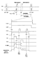
図3は、本実施形態で用いる電子シャッタ機能を説明する図である。先にも述べたように、本実施形態においては、撮像部410の光電変換素子(検出部)への露光時間(蓄積時間)を画素単位で調節する。
<About electronic shutter function>
FIG. 3 is a diagram for explaining the electronic shutter function used in the present embodiment. As described above, in this embodiment, the exposure time (accumulation time) for the photoelectric conversion element (detection unit) of the imaging unit 410 is adjusted in units of pixels.
垂直走査部414は、シャッタ画素位置を指定するアドレス情報(具体的には駆動パルスとしての転送ゲートパルスTGv,TGh)を生成する機能要素として、垂直アドレス設定部414aとは別に、シャッタ対象の単位画素(シャッタ画素)の行アドレスを指定する垂直シャッタタイミング制御部414cvと、シャッタ対象の単位画素の列アドレスを指定する水平シャッタタイミング制御部414chとを有するシャッタタイミング制御部414cを備えている。
The
垂直シャッタタイミング制御部414cvからは、行アドレスを指定する駆動パルスφTGvが同一行の全単位画素403に供給され、水平シャッタタイミング制御部414chからは、列アドレスを指定する駆動パルスφTGhが同一列の全単位画素403に供給されるように2次元マトリクス配線構成を採用する。これにより、両駆動パルスφTGv,φTGhで指定された行および列の単位画素403がシャッタ画素として指定される。
The vertical shutter timing control unit 414cv supplies a drive pulse φTGv designating a row address to all
固体撮像素子10としてCMOS撮像素子12を用いた場合、一般的には、その基本的な動作方式から、信号を出力した画素はその時点から再び光電変換して得た信号電荷の蓄積を開始する。このため、撮像面の走査タイミングにしたがって蓄積の期間がずれ、つまり走査線ごとに走査する時間だけ蓄積期間がずれ、いわゆるライン露光(Line Exposure)となる。CCD型とは異なり、同じ期間中に光電変換素子に入射した光を信号電荷として蓄積し、全画素から同時に垂直CCDに読み出すことで蓄積の同時性を満たすグローバル露光(Global Exposure)とはなっていない。
When a
ここで、たとえば、図3に示すように、撮像領域(撮像部12a,410)において、読出行nとシャッタ行ns(ns1,ns2,…,nsv)とをΔs(Δs1,Δs2,…,Δsv)行だけ離す場合を考える。
Here, for example, as shown in FIG. 3, in the imaging region (
電子シャッタの指示を受けた複数行ns1,ns2,…,nsvの対象列の画素がリセットされてから再び信号電荷の蓄積を開始するので、たとえば撮像面の走査方向が上から下になっている場合、行nと行n+Δsの時間差はフレームレートと走査線数との間で所定の関係を持ち、読出行nとシャッタ行nsの間隔を調整することで、CMOS撮像素子12から読み出される信号の蓄積時間を、ライン周期(1水平走査期間)を調整単位として変えることができる。 Since the accumulation of signal charges starts again after the pixels in the target column of the plurality of rows ns1, ns2,..., Nsv that have received an instruction from the electronic shutter are reset, for example, the scanning direction of the imaging surface is from top to bottom. In this case, the time difference between the row n and the row n + Δs has a predetermined relationship between the frame rate and the number of scanning lines. By adjusting the interval between the readout row n and the shutter row ns, The accumulation time can be changed using the line period (one horizontal scanning period) as an adjustment unit.
ここで、従来のCMOSセンサでは、シャッタ行nsを1つとすることで、電子シャッタ制御を行単位で行なうようにするが、本実施形態では、シャッタタイミング制御部414cにてシャッタ行nsをns1,ns2,…,nsvというように必要な分だけ設定にする。このとき、各列において、1つの単位画素403がシャッタ画素となるが、蓄積時間を同じにする単位画素403は、シャッタ行の位置が同じになる。
Here, in the conventional CMOS sensor, electronic shutter control is performed in units of rows by setting one shutter row ns. In this embodiment, the shutter
垂直アドレス設定部414aで設定されたある時点の読出行nに対して、シャッタタイミング制御部414cにて、全列(H1,H2,…,Hh)の画素に関して、読出行nを除く何れかの行位置、すなわちΔs(Δs1,Δs2,…,Δsv)行だけ離れた位置(時点)においてシャッタ行nsを設定して画素をリセットする。このリセット動作は、シャッタタイミング以前に光電変換素子に蓄積された電荷を掃き捨てることで実現でき、CMOS撮像素子12の場合、転送ゲートをオンさせることで実現できる(詳細は後述する)。
For the readout row n at a certain point set by the vertical
シャッタ行ns1,ns2,…,nsvの画素が垂直アドレス設定部414aによって次に読出行nに設定されるまでの時間が蓄積時間となる、すなわち読出行nとシャッタ行ns1,ns2,…,nsvとの時間間隔が蓄積時間となる。こうすることで、結果的には、画素ごとに蓄積時間を制御できるようになる。
The time until the pixels of the shutter rows ns1, ns2,..., Nsv are next set to the readout row n by the vertical
CMOS撮像素子12が持つライン露光の特質を利用して、電子シャッタ用の駆動パルスφTGv,φTGhを各単位画素403に個別に供給することで、読出行nとシャッタ行n+Δsの時間差を、各列それぞれ1つの単位画素403に設定することができ、簡単に、画素ごとに蓄積時間を制御できる。同一行について共通に駆動パルスφTGvを、また同一列について共通に駆動パルスφTGhを供給することができ、各単位画素403に対する駆動パルスφTGv,φTGh用の配線数が少なくてもよく、この点は、グローバル露光となるCCD型とは大きく異なるところである。
By utilizing the characteristics of line exposure that the
なお、図3では、1フィールド内で露光時間を調整する例を示したが、複数フィールドを利用して露光時間を調整するようにすることもできる。この場合、行それぞれ、通常は1フィールド(1/60秒程度)で1回の読出しを行なうので、たとえば、R,G,Bのカラー画素の内でホワイトバランスゲインに見合った露光時間が最短となるカラー画素に関しては露光時間を無調整にし(ホワイトバランスゲインを1にすることと等価)、残りのカラー画素についてのみ、ホワイトバランスゲインに見合った露光時間となるように、より長い時間に調整(ホワイトバランスゲインを1よりも大きくすることと等価)すればよい。 Although FIG. 3 shows an example in which the exposure time is adjusted within one field, the exposure time can be adjusted using a plurality of fields. In this case, since each row is normally read once in one field (about 1/60 seconds), for example, the exposure time corresponding to the white balance gain among the R, G, B color pixels is the shortest. For the color pixel, the exposure time is not adjusted (equivalent to setting the white balance gain to 1), and only the remaining color pixels are adjusted to a longer time so that the exposure time matches the white balance gain ( Equivalent to making the white balance gain larger than 1).
<単位画素の回路構成例と駆動回路との関係>
図4は、単位画素403の一構成例と、単位画素403を駆動する電子シャッタ機能に関わる駆動回路(図2の垂直走査部414、特にシャッタタイミング制御部414c)との関係を説明する図である。単位画素403は、寄生容量を持った拡散層を主要部に持つフローティングディフュージョン(FDA;Floating Diffusion)438を電荷蓄積部として利用する構成を採りつつ、単位画素に4つのトランジスタ(TRansistor)を有する4トランジスタ型画素構成(以下4TR構成という)のものとなっている。
<Relationship between unit pixel circuit configuration example and drive circuit>
FIG. 4 is a diagram for explaining a relationship between a configuration example of the
図示するように、単位画素403は、光を電荷に変換する光電変換機能とともに、その電荷を蓄積する電荷蓄積機能の各機能を兼ね備えた電荷生成部432と、電荷生成部432に対して、電荷転送部(電荷読出部/転送ゲート部/読出ゲート部)の一例である読出選択用トランジスタ434、リセットゲート部の一例であるリセットトランジスタ436、垂直選択用トランジスタ440、およびフローティングディフュージョン438の電位変化を検出する検知素子の一例であるソースフォロア構成の増幅用トランジスタ442を有する。
As shown in the figure, the
単位画素403を構成する増幅用トランジスタ442は各垂直信号線453(図2の垂直信号線418に相当)に接続されており、また垂直信号線453は垂直列ごとに定電流源Inをなす負荷MOSトランジスタ427のドレインに接続され、また各負荷MOSトランジスタ427のゲート端子には、一定バイアスとして、図示しない負荷制御部からの負荷制御信号Loadが共通に入力されており、信号読出し時には、各増幅用トランジスタ442に接続された負荷MOSトランジスタ427によって、予め決められた定電流を流し続けるようになっている。つまり、負荷MOSトランジスタ427は、そのゲートが一定電位でバイアスされ、選択行の増幅用トランジスタ442とソースフォロアを組むことで、垂直信号線453への信号出力をさせる。
The amplifying
横方向配線は概ね同一行の画素について共通となっており、電子シャッタ制御を伴わない通常駆動時には、垂直走査部414の垂直駆動部414bによって同一行の全単位画素403が同時に駆動制御される。たとえば、垂直駆動部414b内には、転送駆動バッファ452、リセット駆動バッファ454、および選択駆動バッファ456が収容されている。
The horizontal wiring is generally common to pixels in the same row, and during normal driving without electronic shutter control, all
読出選択用トランジスタ434は、転送配線(読出選択線)455を介して転送駆動バッファ452により駆動されるようになっている。リセットトランジスタ436は、リセット配線456を介してリセット駆動バッファ454により駆動されるようになっている。垂直選択用トランジスタ440は、垂直選択線452を介して選択駆動バッファ456により駆動される。
The
また、本実施形態特有の構成要素として、垂直走査部414からは、少なくとも露光時間調整用の転送ゲートパルスが行ごとではなく画素ごとに転送駆動バッファ452に向けて供給されるようにする。必要に応じて、リセットトランジスタ436に向けて露光時間調整用のリセットゲートパルスRGが画素ごとに供給されるようにすることもできる。
Further, as a component unique to this embodiment, at least the transfer gate pulse for adjusting the exposure time is supplied from the
たとえば、垂直走査部414は、通常走査に関わる読出行を設定する垂直アドレス設定部(通常走査)414aの他に、蓄積時間(露光時間)を画素ごとに制御する専用の機能部として、垂直アドレス設定部414aにおける通常動作時と同様にシャッタ対象の単位画素(シャッタ画素)の行選択をするための転送ゲートパルスTGvを出力する垂直シャッタタイミング制御部414cvと、シャッタ対象の単位画素の水平方向(列)の位置の選択を行なうための転送ゲートパルスTGhを出力する水平シャッタタイミング制御部414chとを有し、通常の読出行とシャッタ画素との行間隔(すなわちシャッタ画素の行位置)を指定しつつ、シャッタ画素のカラム位置を指定するシャッタタイミング制御部414cを備えている。
For example, in addition to the vertical address setting unit (normal scanning) 414a for setting a readout row related to normal scanning, the
水平シャッタタイミング制御部414chは、垂直アドレス設定部414aが通常の読出行を指示する際には、1行分の全単位画素403が同時に動作するように、転送ゲートパルスTGhをアクティブにする。
The horizontal shutter timing control unit 414ch activates the transfer gate pulse TGh so that all the
また、このシャッタタイミング制御部414cの構成に応じて、垂直駆動部414bは、少なくとも転送駆動バッファ452に関しては、通常の読出行およびシャッタ画素の選択行に関して読出選択用トランジスタ434を駆動する転送駆動バッファ452vと、シャッタ画素のカラム位置に関して読出選択用トランジスタ434を駆動する転送駆動バッファ452hとを有している。
Further, in accordance with the configuration of the shutter
転送駆動バッファ452vは、垂直アドレス設定部414aからの通常の読出行を指定する読出パルス(転送ゲートパルス)TGと、垂直シャッタタイミング制御部414cvからのシャッタ画素の行を指定する転送ゲートパルスTGvに対して論理和回路を構成して動作するようになっている。
The
また、単位画素403は、各転送駆動バッファ452v,452hからの駆動パルスTGv,TGhを受けて垂直および水平の各方向のシャッタ画素の読出選択用トランジスタ434のゲートに駆動パルスを供給するスイッチ部439を画素ごとに備えている。
The
スイッチ部439は、垂直アドレス設定部414aからの通常の読出行を指定する読出パルス(転送ゲートパルス)TGや垂直シャッタタイミング制御部414cvからのシャッタ画素の行を指定する転送ゲートパルスTGvと、水平シャッタタイミング制御部414chからのカラム位置(特にシャッタ画素のもの)を指定する転送ゲートパルスTGhに対して論理積回路を構成して動作するようになっている。ここで“特にシャッタ画素のもの”と言ったのは、実質的な論理積の効果は、シャッタ画素の行位置と列位置とを指定することにあるからである。
The
また、単位画素403は、増幅用トランジスタ442や電荷蓄積部の機能を備えた電荷注入部の一例であるフローティングディフュージョン438からなるFDA(Floating Diffusion Amp)構成の画素信号生成部405を有するものとなっている。画素信号生成部405は、単位信号としての画素信号を生成する単位信号生成部の一例である。フローティングディフュージョン438は寄生容量を持った拡散層を主要部に持つ。
The
画素信号生成部405におけるリセットトランジスタ436は、ソースがフローティングディフュージョン438に、ドレインが電源VDDにそれぞれ接続され、ゲート(リセットゲートRG)にはリセットパルスRSTがリセット駆動バッファ454から入力される。
In the reset transistor 436 in the pixel signal generation unit 405, the source is connected to the floating
ここで、この単位画素403は、増幅用トランジスタ442と直列に挿入された選択用トランジスタを含んで画素を選択する4TR構成の画素であるが、増幅用トランジスタ442と垂直選択用トランジスタ440のうち、垂直選択用トランジスタ440の方が垂直信号線453側にあるタイプである。
Here, the
すなわち、増幅用トランジスタ442は、ドレインが電源VDD(たとえば2.5V)に、ソースが垂直選択用トランジスタ440のドレインにそれぞれ接続され、ゲートがフローティングディフュージョン438に接続されている。垂直選択用トランジスタ440は、ゲート(特に垂直選択ゲートSELVという)が垂直選択線452に接続され、ソースは画素線451を介して垂直信号線453に接続されている。垂直選択線452には、選択駆動バッファ456から垂直選択信号が印加される。
That is, the amplifying
このような構成では、フローティングディフュージョン438は増幅用トランジスタ442のゲートに接続されているので、増幅用トランジスタ442はフローティングディフュージョン438の電位(以下FD電位という)に対応した信号を、画素線451を介して垂直信号線453に出力する。
In such a configuration, since the floating
リセットトランジスタ436は、フローティングディフュージョン438をリセットする。読出選択用トランジスタ(転送トランジスタ)svは、電荷生成部432にて生成された信号電荷をフローティングディフュージョン438に転送する。垂直信号線453には多数の画素が接続されているが、画素を選択するのには、選択画素のみ垂直選択用トランジスタ440をオンする。すると同一行の選択画素のみが垂直信号線453と接続され、垂直信号線453には、同一行の選択画素の信号が同時に出力される。
The reset transistor 436 resets the floating
なお、図示を割愛するが、増幅用トランジスタ442と垂直選択用トランジスタ440のうち、増幅用トランジスタ442の方が垂直信号線453側にあるタイプのものとすることもできる。
Although not shown in the drawing, the amplifying
ここで、本実施形態においては、電荷蓄積時間を画素ごとに制御するシャッタタイミング制御部414cは、転送駆動バッファ452および転送配線(読出選択線)455を介して、所定行上の所定カラム位置の単位画素403の読出選択用トランジスタ434を制御する。読出行の制御は行単位の制御となるが、シャッタ画素は、行位置だけでなく水平(列;カラム)位置の制御も実行可能であるので、露光時間が画素ごとに制御できる。
Here, in the present embodiment, the shutter
蓄積時間を制御するシャッタタイミング制御部414cと、通常読出しのアドレス位置(行)を制御する垂直アドレス設定部414aとで、担当する行を分けて蓄積時間を制御するようにしている。垂直列方向を露光時間設定に使い、読出行上の複数の画素において、一方の画素は長時間蓄積に割り当て、他方の画素は短時間蓄積に割り当てるようにすることができる。
The storage timing is controlled by dividing the assigned line by the shutter
こうすることで、画素ごとに蓄積時間を自由に設定できるようになるので、短時間蓄積側も蓄積時間に自由度が生まれる。これにより、電荷蓄積時間の設定の自由度が大幅に広がるので、使い勝手がよくなる。ただし、図3にて説明したように、露光・蓄積期間(シャッタ期間)の制御はライン周期を1調整単位として行なうことになる。 By doing so, the accumulation time can be freely set for each pixel, so that the short time accumulation side also has a degree of freedom in the accumulation time. As a result, the degree of freedom in setting the charge accumulation time is greatly expanded, and the usability is improved. However, as described with reference to FIG. 3, the control of the exposure / accumulation period (shutter period) is performed with the line cycle as one adjustment unit.
また、このような蓄積時間設定を、垂直アドレス設定部414aだけで行なうのではなく、電子シャッタ専用のシャッタタイミング制御部414cを設けて蓄積時間を制御するようにしているので、その制御が容易になる。
Further, such accumulation time setting is not performed only by the vertical
なお、行単位での露光時間制御を行なうのではなく、たとえば同一水平期間内で、長時間蓄積側の画素信号の読み出しを行なった後に、短時間蓄積を行ない、直ぐにその短時間蓄積側の画素信号の読み出しを行なうようにすることもできる。ただしこの場合、短時間蓄積側は、1水平期間(たとえば64マイクロ秒)以下の蓄積時間となるので、短時間側の蓄積時間の設定に自由度がない。 In addition, instead of performing exposure time control in units of rows, for example, after reading out the pixel signal on the long-time accumulation side within the same horizontal period, the short-time accumulation is performed, and the pixel on the short-time accumulation side is immediately It is also possible to read out the signal. However, in this case, since the short-time accumulation side has an accumulation time of one horizontal period (for example, 64 microseconds) or less, there is no flexibility in setting the accumulation time on the short-time side.
<単位画素の駆動方法>
図5および図6は、図4に示した単位画素403を駆動して画素信号(単位画素403から出力される単位信号)を取得する手法を説明するタイミングチャートである。特に、電子シャッタに関して、ライン周期を1調整単位として電子シャッタによる露光時間制御を行なう場合について説明するものである。なお、図5は、蓄積時間の制御に際して機械式のシャッタ52を併用しない場合であり、図6は、機械式のシャッタ52を併用する場合を示している。
<Driving method of unit pixel>
FIG. 5 and FIG. 6 are timing charts for explaining a method of acquiring the pixel signal (unit signal output from the unit pixel 403) by driving the
図4に示した4TR構成では、リセットトランジスタ436は、フローティングディフュージョン438をリセットする。具体的には、フローティングディフュージョンの信号電荷(ここでは電子)を電源配線に捨てることによって、フローティングディフュージョン438をリセットする。
In the 4TR configuration shown in FIG. 4, the reset transistor 436 resets the floating
読出選択用トランジスタ(転送トランジスタ)svは、電荷生成部432にて生成された信号電荷を、電荷蓄積部の一例であるフローティングディフュージョン438に転送する。
The read selection transistor (transfer transistor) sv transfers the signal charge generated by the charge generation unit 432 to a floating
フローティングディフュージョン438は単位信号生成部の一例である増幅用トランジスタ442のゲートに接続されているので、増幅用トランジスタ442はフローティングディフュージョン438の電位(以下FD電位ともいう)に対応した信号(この例では電圧信号)を、垂直選択用トランジスタ440がオンしているときに、画素線451を介して出力信号線の一例である垂直信号線453に出力する。すなわち、垂直信号線453には多数の画素が接続されているが、画素を選択するのには、選択画素のみ垂直選択用トランジスタ440をオンする。すると選択画素のみが垂直信号線453と接続され、垂直信号線453には選択画素の信号が出力される。
Since the floating
具体的には、図5のタイミングチャートに示すように、読出パルス(転送ゲートパルス)TGがアクティブ(本例ではハイレベル)となり、読出選択用トランジスタ434を駆動し、電荷生成部432に入射した光が光電変換されて生成された信号電荷を、蓄積ノードとして機能するフローティングディフュージョン438に移送して読み出す。
Specifically, as shown in the timing chart of FIG. 5, the read pulse (transfer gate pulse) TG becomes active (high level in this example), drives the
ここで、電荷生成部432に入射した光が光電変換されて生成された信号電荷は、読出選択用トランジスタ434がオンするまで電荷生成部432に蓄積される。したがって、画素信号を読み出す前の読出選択用トランジスタ434をオンするタイミング(ts)を調整することで、露光時間を電子シャッタ動作で制御することができるようになる。シャッタタイミング(たとえばts1,ts2)とその後の通常通りに選択する読出行(t10〜t20に対応)とで、シャッタ画素の時間間隔を調節することにより、撮像部12aの単位画素403への露光時間(蓄積時間)を調節することができるようになる。
Here, the signal charge generated by photoelectric conversion of the light incident on the charge generation unit 432 is accumulated in the charge generation unit 432 until the
なお、シャッタタイミング(たとえばts1,ts2)時には、シャッタタイミング制御部414cから、転送駆動バッファ452に向けて露光時間調整用の転送ゲートパルスTGを供給して、それ以前に電荷生成部432にて生成された信号電荷をフローティングディフュージョン438に転送しておく。必要に応じて、リセットトランジスタ436に向けて露光時間調整用のリセットゲートパルスRGを供給することで、画素信号の読出処理(t10〜t20に対応)に先立って、シャッタタイミング(たとえばts1,ts2)時にフローティングディフュージョン438に転送された信号電荷を掃き捨てておく。
At the shutter timing (for example, ts1, ts2), a transfer gate pulse TG for adjusting the exposure time is supplied from the shutter
読出行(t10〜t20に対応)における画素信号の読出し時に水平走査線帰線期間にまず行なわれるのは、垂直選択パルスSELをアクティブ(本例ではハイレベル)にして垂直選択用トランジスタ440をオンさせ(t10)、増幅用トランジスタ442でフローティングディフュージョン438の電荷を検出できるように、読出し行の増幅用トランジスタ442の出力と垂直信号線453とを接続して、垂直信号線453、電流源In(負荷MOSトランジスタ427)、および増幅用トランジスタ442でソースフォロワ回路を構成する。垂直信号線453の電位は、フローティングディフュージョン438の電位変動に追従する。これにより、フローティングディフュージョン438の電荷量に対応する、増幅用トランジスタ442のゲート電位で決まる電位のみが垂直信号線453に伝達される。
When reading out pixel signals in the readout row (corresponding to t10 to t20), the first thing to be done in the horizontal scanning line blanking period is to activate the vertical selection pulse SEL (high level in this example) and turn on the
また、水平走査線帰線期間の開始とともに、シャッタタイミング(たとえばts1,ts2)後に電荷生成部432に信号電荷Qsig が蓄積された状態で、最初に画素信号生成部5を基準電圧にリセットする、つまりリセットゲートパルスRGをアクティブ(本例ではハイレベル)にして(t11)、リセットトランジスタ436をオンさせることで、フローティングディフュージョン438に蓄積された暗電流積分値を排出させる。これによって、フローティングディフュージョン438は、電源電圧値(Vdd)に設定される。
Also, with the start of the horizontal scanning line blanking period, the pixel signal generation unit 5 is first reset to the reference voltage in a state where the signal charge Qsig is accumulated in the charge generation unit 432 after the shutter timing (for example, ts1, ts2). That is, the reset gate pulse RG is activated (high level in this example) (t11), and the reset transistor 436 is turned on to discharge the dark current integrated value accumulated in the floating
電子シャッタ動作時には、シャッタタイミング(たとえばts1,ts2)時に掃き出された信号電荷がフローティングディフュージョン438に存在するが、その分も掃き出される。したがって、シャッタタイミング(たとえばts1,ts2)時にフローティングディフュージョン438に転送された信号電荷を、シャッタタイミング(たとえばts1,ts2)の直後に掃き捨てておくことは必須ではない。なお、リセットゲートパルスRGをインアクティブ(本例ではローレベル)にすると(t12)、カップリングにより、フローティングディフュージョン438の電位が若干落ちる。
During the electronic shutter operation, the signal charge swept out at the shutter timing (for example, ts1, ts2) is present in the floating
このとき、駆動制御部12cからサンプルパルスSHPが出力されて、アナログフロントエンド部12b内のCDS機能部をなすシフトトランジスタのゲートに供給され、各シフトトランジスタがオンする。すなわち、駆動制御部12cからクランプパルスSHDが供給され、CDS機能部をなすクランプトランジスタのゲートに供給されて、各クランプトランジスタがオンし、リセットレベルSrst が検出される(t14)。
At this time, a sample pulse SHP is output from the
次に、電荷生成部432についての読出選択用トランジスタ434を駆動して、電荷生成部432から信号電荷Qsig に応じた信号成分Soを読み出す。すなわち、転送ゲートパルスTGをハイレベルにして(t16)、読出選択用トランジスタ434をオンさせ、電荷生成部432に蓄積されていた信号電荷Qsig をフローティングディフュージョン438に移送する。このフローティングディフュージョン438に移送された信号電荷Qsig の電荷量は、増幅用トランジスタ442によって検出され、その電荷量に応じた電位が発生されて垂直信号線453に伝達される。
Next, the
この後、駆動制御部12cからクランプパルスSHDを供給して(t18)、クランプトランジスタをオンさせて、電荷生成部432が検出した信号電荷Qsig に応じた画素信号レベルSsig を検出する。
Thereafter, the clamp pulse SHD is supplied from the
ここで、アナログフロントエンド部12bのカラム処理部では、リセットレベルSrst と画素信号レベルSsig との差分をとることで、オフセット成分が取り除かれ、真の信号成分Soを検知できる。画素ごとの固定パターンノイズの除去を行なうことができる。
Here, the column processing unit of the analog
信号電荷の転送が終わり、十分時間が経った後には、垂直選択パルスSELをインアクティブ(本例ではローレベル)にする(t20)。 After the signal charge transfer is completed and a sufficient time has passed, the vertical selection pulse SEL is made inactive (low level in this example) (t20).
なお、図6に示すように、機械式のシャッタ52を併用すると1水平期間(HS;ライン周期)内でシャッタ52を開くことができる。よって、電子シャッタのみで露光時間制御を行なうとライン周期を1調整単位としなければならないのに対して、機械式のシャッタ52を併用すれば、露光時間の制御の自由度が大きくなり、ライン周期内で露光時間の微調整ができるようになる。
As shown in FIG. 6, when the
ただし、機械式のシャッタ52の効果は全画素に寄与する点に考慮する必要がある。たとえば、AGC調整や、ガンマ補正に関しては、従来通り、固体撮像素子10から出力された画素信号に対して信号レベルを大きくする増幅処理を伴う信号処理を用いつつ、ホワイトバランス調整に関してのみ、理対象の信号レベルを大きくする処理を伴う増幅によってノイズも増幅されることに起因してS/N劣化を招く問題を避けつつ(抑制しつつ)ホワイトバランスが取れるようにするべく露光時間を制御する手法を採用する場合を考える。この場合、R,G,Bのカラー画素の内、露光時間を同じにしたときに最も信号レベルの小さいカラー画素に関して機械式のシャッタ52を併用して、ライン周期内で露光時間の微調整をすればよい。
However, it is necessary to consider that the effect of the
<<信号処理機能>>
図7は、上記デジタルスチルカメラ1における、信号レベルを大きくする処理を伴う画像信号処理機能に着目したブロック図である。
<< Signal processing function >>
FIG. 7 is a block diagram that focuses on an image signal processing function that involves a process of increasing the signal level in the digital
図示するように、信号処理系6は、CDS処理部62aおよびAGC処理部62bを有するプリアンプ部62とAD変換部64とを具備した前段の信号処理系6aと、画像処理部(DSP)66で構成された後段の信号処理系6bとを備える。
As shown in the figure, the signal processing system 6 includes a signal processing system 6a in the preceding stage including a
AGC処理部62bでは、CMOS撮像素子12の個々の光電変換素子(電荷検出部)の感度ばら付き(感度バラツキ)を補正し、かつAD変換部64に対して適正入力レベルになるようゲインを調整する。
In the
後段の信号処理系6bすなわち画像処理部(DSP)66における信号処理機能としては、固体撮像素子10で取得されAD変換部64にてデジタル化された撮像データの黒基準をクランプするデジタルクランプ部200、デジタルクランプ部200にてクランプされた撮像データからR,G,Bの原色データを抽出するとともに同時化する原色分離・同時化処理部202、および周辺画素のデータを用いて画素を補う画素補間処理部204、画素データのゲインを調整可能な色信号増幅部の一例であるホワイトバランスアンプ部210を備えている。なお、画素補間処理部204とホワイトバランスアンプ部210とは、配置順を逆にしてもよい。
As a signal processing function in the subsequent signal processing system 6b, that is, the image processing unit (DSP) 66, a
原色分離・同時化処理部202は、固体撮像素子10が補色フィルタを使用するものである場合にデジタルクランプ部200から供給されるデジタル画像信号をR(赤),G(緑),B(青)の原色信号であるR信号Sr1,G信号Sg1,B信号Sb1に分離し、これらを画素補間処理部204に供給する。
The primary color separation /
画素補間処理部204は、固体撮像素子10(CMOS撮像素子12)における画素数と同じ画素数のイメージファイルを生成するべく、ある画素位置において存在しない色成分を周辺画素から推測して画素信号を補う。たとえば、R(赤)画素からはRの信号成分を取得できるがG(緑),B(青)の信号成分を取得できないので、その周りにある画素から補間画素G,Bの各画素信号を推測して取得する。この際には、たとえば周辺画素の信号の単純平均で補間画素の信号成分を求めることもできるが、解像度や偽信号を考慮した適応処理にするとなおよい。
In order to generate an image file having the same number of pixels as the number of pixels in the solid-state imaging device 10 (CMOS imaging device 12), the pixel
ホワイトバランスアンプ210としては、各色用に個別にホワイトバランスアンプ210R,210G,210Bが設けられており、一般的な被写体を撮像した場合、画面全体にさまざまな色成分が無作為に存在するため、画面全体の色成分を全て積分すると、色信号(たとえばR,G,B)の各要素がほぼ等しく抽出される、あるいは色差成分の積分値がゼロになるであろうことを考慮し、これを制御の目標、すなわち無彩色に近づけるべくアンプゲインを調整する。すなわち、撮影時の光源で白を撮影した場合に出力映像が白(R:G:B=1:1:1)になるようRGB各画素のレベルを調整する。この際には、少なくとも1色については信号レベルを増幅する処理を伴う。
As the white balance amplifier 210,
また画像信号処理部66は、ホワイトバランスアンプ部210で取得された原色データR,G,Bに対して、輝度信号処理や色信号処理を施して輝度データY(あるいは明度データL)や2つの色データU,Vに変換して出力する信号処理部220を備えている。信号処理部220にて生成された各データY,U,Vは、記録系7に送られて画像記録に供されたり、あるいは表示系8に送られて表示出力に供されたりする。
The image
信号処理部220は、一例として、ガンマ補正部222および色差マトリクス部224を備えている。もちろん、この構成例は一例であって、これらの処理機能以外の構成要素も備える。
For example, the
ガンマ補正部222は、R信号Sr3,G信号Sg3,B信号Sb3に基づいて、忠実な色再現のためのガンマ(γ)補正を行ない、ガンマ(γ)補正された各色用の出力信号R,G,Bを色差マトリクス部224に入力する。たとえば、ガンマ補正部222は、ガンマ補正値の初期値を図示しないメモリテーブルに持っており、外部からガンマ補正値を変更することもできる。
The
色差マトリクス部224は、色差マトリクス処理を行なって得た色差信号R−Y,B−Yをビデオエンコーダ86に入力する。
The color difference matrix unit 224 inputs the color difference signals RY and BY obtained by performing the color difference matrix processing to the
ビデオエンコーダ86は、色信号副搬送波に対応するデジタル信号で色差信号R−Y,B−Yをデジタル変調した後、図示しない輝度信号生成部にて生成された輝度信号Yと合成して、デジタル映像信号VD(=Y+S+C;Sは同期信号、Cはクロマ信号)に変換した後、DA変換部82に入力する。DA変換部82は、デジタル映像信号VDをアナログ映像信号Vに変換する。
The
また画像信号処理部66は、本実施形態の特徴部分として、本撮影に先立って行なわれる準備段階としての先行撮影(仮撮像)時に取得されるAGC処理部62b、ホワイトバランスアンプ部210、およびガンマ補正部222からのデータを参照して、信号処理部220を経て出力される映像信号の増幅量(ゲイン)を画素単位で解析するゲイン解析部230を備えている。
Further, the image
ゲイン解析部230は、トータルゲインGAtotal を一括して求めてもよいが、たとえば、AGC処理に関するAGCゲインGAagc 、ホワイトバランス調整に関するホワイトバランスゲインGAwb、ガンマ補正に関するガンマゲインGAgamma を個別に求め、それらの積(GAagc *GAwb*GAgamma )でトータルゲインGAtotal を求めてもよい。ゲイン解析部230は、この解析結果に基づいて、撮像部12aから出力される画素信号が、AGC、ホワイトバランス調整、あるいはガンマ補正量に見合った出力信号レベルになるような露光時間を画素ごとに求め、この求めた露光時間情報を、所定の図示しない記憶部に保持する。
The
また、カメラモジュール3側には、ゲイン解析部230の解析結果に基づいて、撮像部12aから出力される画素信号が、AGC、WB、あるいはガンマ補正量に見合った出力信号レベルになるよう、カメラモジュール3側の駆動パルスのタイミングを制御するタイミング制御部91(駆動制御部12c,407に相当)を備えている。
In addition, on the camera module 3 side, based on the analysis result of the
ゲイン解析部230とタイミング制御部91とで、単位構成要素としての単位画素403から出力された画素信号のレベルを大きくする増幅信号処理に代えて、増幅信号処理に伴うS/N劣化を抑制しつつ、この増幅信号処理における増幅率に応じたレベルの画素信号が各カラー(R,G,B)の単位画素403から出力されるように、光電変換素子(検出部)における検出時間(露光時間)を調整する制御部が構成される。
The
また、このゲイン解析部230とタイミング制御部91を備えた制御部を含み、かつカメラモジュール3における固体撮像素子10や光学系5の部材(撮像レンズ50やシャッタ52)を除いて、本発明に係る信号処理装置が構成される。そして、ゲイン解析部230とタイミング制御部91を備えた制御部を含み、さらにカメラモジュール3における固体撮像素子10を含んで、本発明に係る物理量分布検知のための装置が構成される。
Further, the present invention includes the control unit including the
ここで、ゲイン解析部230は、たとえば、ホワイトバランス制御機能に着目すれば、フィールドごとの色信号(原色信号や色差信号)の積分値を求めてホワイトバランスの制御情報を生成する。
Here, for example, when paying attention to the white balance control function, the
ゲイン解析部230は、解析結果に基づいて、撮像部12aから出力される画素信号が、AGC、WB、あるいはガンマ補正量に見合った出力信号レベルになるよう、カメラモジュール3側のタイミング制御部91(駆動制御部12c,407に相当)と協働して、画素ごとにリセットゲートパルスRGと転送ゲートパルスTG(読出しパルス)の間隔を調整して露光時間を決める電子シャッタスピード制御を行なうことで、本撮影時の電荷蓄積量を制御する。
Based on the analysis result, the
たとえば、露光時間を長くすることで、撮像部12aの光電変換素子から出力される信号のレベルを大きくする処理を行なうことができるので、S/N劣化の問題を避けつつ、実質的には、信号レベルを大きくする処理を伴う画像信号処理を実行することができるようになる。R,G,B画素の露光時間を個別に制御することで、AGC処理、ホワイトバランス調整、およびガンマ補正を画素ごとに行なうことができ、かつ、AGC処理、ホワイトバランス調整、およびガンマ補正に当たっては、事実上、CMOS撮像素子12から出力された画素信号に対して信号レベルを増大させる処理を行なわないので、AGC処理やホワイトバランス調整あるいはガンマ補正による回路ゲインで発生するS/N劣化を抑制することができる。
For example, by increasing the exposure time, it is possible to perform processing to increase the level of the signal output from the photoelectric conversion element of the
また信号処理系6は、先行撮影と本撮影との信号伝達ルートを切り替えるべく、CDS処理部62aとAGC処理部62bとの間に1入力(312a)−2出力(312b,c)型の切替スイッチ312を備える。切替スイッチ312の一方の出力端子312bはAGC処理部62bに接続され、他方の出力端子312cはAD変換部64に接続されている。
Further, the signal processing system 6 switches between a 1-input (312a) -2 output (312b, c) type between the
同様に、先行撮影と本撮影との信号伝達ルートを切り替えるべく、画素補間処理部204とホワイトバランスアンプ部210との間に、1入力(314a)−2出力(314b,c)型の切替スイッチ314をR,G,Bそれぞれの系統に備える。切替スイッチ314の一方の出力端子314bはホワイトバランスアンプ部210に接続され、他方の出力端子314cは色差マトリクス部224に接続されている。
Similarly, a 1-input (314a) -2 output (314b, c) type changeover switch is provided between the pixel
なお、図示を割愛するが、先行撮影と本撮影との信号伝達ルートを切り替えるべく、ホワイトバランスアンプ部210とガンマ補正部222との間に、1入力−2出力型の切替スイッチ316(図示せず)をR,G,Bそれぞれの系統に設けてもよい。この場合、切替スイッチ314の他方の出力端子314cはホワイトバランスアンプ部210の出力と同様に切替スイッチ316の入力端子316aに接続されるようにする。また、切替スイッチ316の一方の出力端子316bはガンマ補正部222に接続され、他方の出力端子316cは色差マトリクス部224に接続されるようにする。
Although not shown, a 1-input-2-output type changeover switch 316 (not shown) is provided between the white balance amplifier unit 210 and the
各切替スイッチ312,314,316(図示せず)は、全てが連動して先行撮影と本撮影との信号伝達ルートを切り替えるように共通の制御信号で制御してもよいし、それぞれ個別に先行撮影と本撮影との信号伝達ルートを切り替えるように個別の制御信号で制御してもよい。
Each change-over
個別の制御信号で各切替スイッチ312,314,316を制御すれば、AGC、ホワイトバランス調整制御、ガンマ補正の何れか(複数でもよい)の処理に関しては従来通り固体撮像素子10から出力された画素信号に対して信号レベルを大きくする処理を伴う処理を実行しつつ、残りの処理に関しては、調整ゲインに見合った露光時間となるように、画素ごとに、それぞれ独立に露光時間を制御することができる。
If each of the
<動作説明>
次に、準備工程(仮撮像)および本工程の詳細について説明する。先ず、準備工程(仮撮像)段階として、ゲイン解析部230は、CDS処理部62aの出力信号がAGC処理部62bを通るように、切替スイッチ312を出力端子312b側にセットするとともに、画像信号処理部66の信号がホワイトバランスアンプ部210およびガンマ補正部222を通るように、切替スイッチ314を出力端子314b側にセットする。
<Description of operation>
Next, details of the preparation step (provisional imaging) and the main step will be described. First, as a preparatory process (temporary imaging) stage, the
準備工程では、機械式のシャッタ52を開き、RGB信号を取得する。なお、この準備工程のタイミングは、たとえば、ユーザがシャッタボタンを半押ししたことをもって判断するとよい。
In the preparation step, the
このとき、CMOS撮像素子12からの電気信号は、CDS処理部62aおよびAGC処理部62bを通り画素ごとのAGCゲインGAagc で増幅された後、AD変換部64から画像信号処理部66に入る。画像信号処理部66では、デジタルクランプ部200、原色分離・同時化処理部202、画素補間処理部204、およびホワイトバランスアンプ部210を通り、ホワイトバランスが取れるようにRGB各色のホワイトバランスゲインGAwbがそれぞれ決められる。さらに、ガンマ補正部222にて信号レベル(被写体輝度)に応じた画素ごとのガンマゲインGAgamma でガンマ補正が加えられる。
At this time, the electric signal from the
次に、演算工程段階として、ゲイン解析部230は、AGC処理部62b、ホワイトバランスアンプ部210、並びにガンマ補正部222での総合的なゲイン値をCMOS撮像素子12の画素単位で分析する。また、その分析結果と同等のゲイン分を電子シャッタスピード制御を用いて固体撮像素子10(CMOS撮像素子12)の電荷蓄積量を画素単位で制御できるように、電荷蓄積時間をRGB画素ごとに演算する。そして、露光時間(電荷蓄積時間)を決めるリセットパルスと読出しパルスの制御タイミングを決定して記憶する。
Next, as a calculation process step, the
次にたとえばユーザがシャッタボタンを全押しすると、上記で決定された露光時間で、本工程(本撮影)を実行する。この本工程時には、ゲイン解析部230は先ず、CDS処理部62aの出力信号がAGC処理部62bをスキップしAD変換部64に入るように、切替スイッチ312を出力端子312c側にセットするとともに、画像信号処理部66の信号がホワイトバランスアンプ部210およびガンマ補正部222をスキップし色差マトリクス部224に入るように、切替スイッチ314を出力端子314c側にセットする。
Next, for example, when the user fully presses the shutter button, this step (main photographing) is executed with the exposure time determined above. In this process, the
次にゲイン解析部230とタイミング制御部91は協働して、記憶しておいた準備工程時の分析結果と同等のゲイン分が加味されてCMOS撮像素子12から画素信号が出力されるように、画素単位で電荷蓄積時間を制御する。これによって、分析結果と同等のゲイン分を与える画素信号がCMOS撮像素子12から出力される。
Next, the
これら分析結果と同等のゲイン分が与えられた画素信号は、CDS処理部62aを通り、切替スイッチ312を介してAGC処理部62bをスキップしAD変換部64に入る。この後、画素補間処理部204を通り切替スイッチ314でホワイトバランスアンプ部210およびガンマ補正部222をスキップして色差マトリクス部224に入り、デジタル映像信号として出力される。
The pixel signal to which a gain equivalent to these analysis results is given passes through the
つまり、通常はCMOS撮像素子12から出力された信号レベルを直接に操作してその信号レベルを大きくする処理を伴う(すなわち電気信号レベルで扱う)AGC処理やホワイトバランス調整あるいはガンマ補正における信号レベル調整を、CMOS撮像素子12から出力された信号そのものに対して操作するのではなく、露光時間制御による蓄積電荷量の増減で行なう。
That is, normally, the signal level output from the
露光時間を長くすることで、撮像部12aの光電変換素子から出力される信号のレベルを大きくする処理を行なうことができるので、S/N劣化の問題を避けつつ、信号レベルを大きくする処理を伴う画像信号処理を実行することができるようになる。
By increasing the exposure time, it is possible to perform processing for increasing the level of the signal output from the photoelectric conversion element of the
ゲイン解析部230における解析で取得したゲインに見合った露光時間となるように、R,G,B画素の露光時間を個別に制御することで、AGC処理、ホワイトバランス調整、およびガンマ補正を行なうことができ、かつ、AGC処理、ホワイトバランス調整、およびガンマ補正に当たっては、事実上、CMOS撮像素子12から出力された画素信号に対して信号レベルを増大させる処理を行なわないので、従来のAGC処理やホワイトバランス調整あるいはガンマ補正による回路ゲインで発生するS/N劣化を抑制することができる。AGC処理やホワイトバランス調整あるいはガンマ補正による回路ゲインで発生するS/N劣化を抑制し再現性の良い映像の取得を実現することができる。
AGC processing, white balance adjustment, and gamma correction are performed by individually controlling the exposure time of R, G, and B pixels so that the exposure time corresponding to the gain acquired by the analysis in the
たとえば、ホワイトバランス調整制御に着目した場合、従来のホワイトバランス調整や準備工程時における通常の信号パスルートでは、撮像デバイス(固体撮像素子10)で得られる被写体を表わす撮像信号の全体が白に近づくように、ホワイトバランスアンプ部210の各ホワイトバランスアンプ210R,210G,210Bにて、原色のR信号Sr1,G信号Sg1,B信号Sb1に対してゲイン調整(ホワイトバランス用のゲイン調整という)を行なってホワイトバランスを取る。
For example, when attention is focused on white balance adjustment control, the entire image pickup signal representing the subject obtained by the image pickup device (solid-state image pickup device 10) approaches white in a normal signal path route during conventional white balance adjustment and preparation steps. Further, the
これに対して、本実施形態の本撮像時には、ホワイトバランスアンプ部210におけるホワイトバランス用のゲイン調整に代えて、準備工程時において解析したホワイトバランス用の各色のゲイン調整値に対応するように、各カラー画素に応じた単位画素403の検出時間(露光時間)を個別(ここでは“色画素ごとに”を意味する)に調整する。露光時間調整によって撮像部12aの光電変換素子から出力される画素信号レベルをR,G,Bのカラー画素ごとに調整するので、単位画素403から出力された画素信号に対して増幅処理を伴うホワイトバランス用のゲイン調整を行なわなくとも、実質的にホワイトバランス用のゲイン調整を行なうことができるので、S/N劣化の問題を避けつつ、ホワイトバランス調整ができる。
On the other hand, at the time of the main imaging of the present embodiment, instead of the white balance gain adjustment in the white balance amplifier unit 210, in order to correspond to the gain adjustment value of each color for white balance analyzed in the preparation process, The detection time (exposure time) of the
また、AGC処理に関しても同様であり、従来のAGC処理や準備工程時における通常の信号パスルートでは、画素ごとにゲインを調整することで、撮像デバイス(固体撮像素子10)の個々の光電変換素子(電荷検出部)の感度ばら付きを補正する。また、AD変換部64に対して適正入力レベルになるようゲインを調整する。たとえば、露光時間不足で画素からの出力電圧が小さい場合に、適切なゲインを設定し、増幅した信号をAD変換部64に入力する。
The same applies to the AGC processing. In the conventional signal path route in the conventional AGC processing and the preparation process, the individual photoelectric conversion elements (in the solid-state imaging device 10) of the imaging device (solid-state imaging device 10) are adjusted by adjusting the gain for each pixel. The sensitivity variation of the charge detection unit) is corrected. Further, the gain is adjusted so that the
これに対して、本実施形態の本撮像時には、AGC処理部62bにおけるAGC処理に代えて、準備工程時において解析したAGC処理用のゲイン調整値に対応するように、各カラー画素に応じた単位画素403の検出時間(露光時間)を個別に調整する。画素ごとに露光時間を調整することで読出時のゲインを画素ごとに可変にする。
On the other hand, at the time of the main imaging in the present embodiment, instead of the AGC processing in the
露光時間調整によって撮像部12aの光電変換素子から出力される画素信号レベルをR,G,Bのカラー画素ごとに調整するので、単位画素403から出力された画素信号に対して増幅処理を伴うAGC処理のゲイン調整を行なわなくとも、実質的にAGC処理用のゲイン調整を行なうことができるので、S/N劣化の問題を避けつつ、AGC処理ができる。
Since the pixel signal level output from the photoelectric conversion element of the
また、ガンマ補正処理に関しても同様であり、従来のガンマ補正処理や準備工程時における通常の信号パスルートでは、光量に対する階調の変化特性を調整し、また、カラー画像処理時には忠実な色再現がなされるように各色のガンマカーブを調整する。 The same applies to the gamma correction processing. In the conventional signal path route during the conventional gamma correction processing and the preparation process, the gradation change characteristic with respect to the light intensity is adjusted, and faithful color reproduction is performed during color image processing. Adjust the gamma curve for each color so that
これに対して、本実施形態の本撮像時には、ガンマ補正部222におけるガンマ補正処理に代えて、準備工程時において解析したガンマ補正処理用のゲイン調整値に対応するように、各カラー画素に応じた単位画素403の検出時間(露光時間)を個別に調整する。露光時間調整によって撮像部12aの光電変換素子から出力される画素信号レベルをR,G,Bのカラー画素ごとに調整するので、単位画素403から出力された画素信号に対して増幅処理を伴うガンマ補正処理のゲイン調整を行なわなくとも、実質的にガンマ補正処理用のゲイン調整を行なうことができるので、S/N劣化の問題を避けつつ、ガンマ補正処理ができる。
On the other hand, at the time of the main imaging in the present embodiment, instead of the gamma correction processing in the
従来のガンマ補正処理では、低輝度の被写体では高輝度の被写体よりも大きな増幅率で信号レベルを増幅するために、S/N劣化の問題が高輝度の被写体よりも大きいのに対して、本実施形態の手法では、処理対象の画素信号レベルを大きくする増幅処理を行なうことなく、露光量の調整によって実質的にガンマ補正処理用のゲイン調整を行なうので、被写体輝度に関わらず(低輝度の被写体においても)、S/N劣化の問題が生じない。S/N劣化の改善効果は、低輝度の被写体ほど高いと言える。 In the conventional gamma correction processing, since the signal level is amplified with a larger amplification factor in a low-luminance subject than in a high-luminance subject, the problem of S / N degradation is larger than that in a high-luminance subject. In the method of the embodiment, the gain adjustment for the gamma correction process is substantially performed by adjusting the exposure amount without performing the amplification process for increasing the pixel signal level to be processed. The problem of S / N degradation does not occur even in the subject. It can be said that the effect of improving the S / N degradation is higher for a low-luminance subject.
ガンマ補正処理は、AGC処理やホワイトバランス調整よりもゲイン調整幅が大きく、しかも、低輝度の被写体ほどゲイン調整幅が大きくなる。この点では、露光量の調整を行なう本実施形態の手法は、ホワイトバランス調整制御やAGC処理よりもガンマ補正処理の方が効果が高いと考えられる。 The gamma correction process has a larger gain adjustment range than the AGC process and white balance adjustment, and the gain adjustment range becomes larger as the subject has a lower luminance. In this respect, it is considered that the gamma correction process is more effective than the white balance adjustment control and the AGC process in the method of the present embodiment that adjusts the exposure amount.
<デジタルスチルカメラの全体構成;CCDタイプ>
図8は、本発明に係る撮像装置の第2実施形態を示す概略構成図である。第2実施形態の撮像装置は、第1実施形態におけるCMOS撮像素子12をたとえばインターライン転送(IT)方式で全画素読出しが可能なCCD撮像素子11に変更しており、この変更に応じて、プリアンプ部やAD変換部を有するアナログフロントエンド部12bおよび駆動制御部12cと同等の機能を持つ回路部を、CCD撮像素子11とは別に設けるように変更している。その他の点は、概ね第1実施形態と同じである。
<Overall configuration of digital still camera; CCD type>
FIG. 8 is a schematic configuration diagram showing a second embodiment of the imaging apparatus according to the present invention. In the image pickup apparatus of the second embodiment, the CMOS
カメラモジュール3内の駆動制御部96には、CCD撮像素子11を駆動するための各種のパルス信号を生成するタイミング信号生成部40と、このタイミング信号生成部40からのパルス信号を受けて、CCD撮像素子11を駆動するためのドライブパルスに変換するドライバ(駆動部)42と、CCD撮像素子11やドライバ42などに電源供給する駆動電源46が設けられている。
A
また、DSPで構成された画像信号処理部66には、CPUなどからなる中央制御部92やEEPROM93dを除く記憶部93の各種メモリ、さらにはCCD撮像素子11の動作タイミングを規定する同期信号を生成する同期信号生成部41を取り込み、CCD撮像素子11を主要部とするカメラモジュール3と、画像信号処理部66やEEPROM93dとを含んで撮像装置モジュール3aを構成するようにしている。
In addition, the image
図示した例は、信号処理系6のプリアンプ部62およびAD変換部64をカメラモジュール3に内蔵しているが、このような構成に限らず、プリアンプ部62やAD変換部64を本体ユニット4内に設ける構成を採ることもできる。またDA変換部を画像信号処理部66内に設ける構成を採ることもできる。
In the illustrated example, the
また、タイミング信号生成部40をカメラモジュール3に内蔵しているが、このような構成に限らず、タイミング信号生成部40を本体ユニット4内に設ける構成を採ることもできる。またタイミング信号生成部40とドライバ42とが別体のものとしているが、このような構成に限らず、両者を一体化させたもの(ドライバ内蔵のタイミングジェネレータ)としてもよい。こうすることで、よりコンパクトな(小型の)デジタルスチルカメラ1を構成できる。
Further, although the timing
また、タイミング信号生成部40やドライバ42は、それぞれ個別のディスクリート部材で回路構成されたものでもよいが、1つの半導体基板上に回路形成されたIC(Integrated Circuit)として提供されるものであるのがよい。こうすることで、コンパクトにできるだけなく、部材の取扱いが容易になるし、両者を低コストで実現できる。また、デジタルスチルカメラ1の製造が容易になる。また、使用するCCD撮像素子11との関わりの強い部分であるタイミング信号生成部40やドライバ42をCCD撮像素子11と共通の基板に搭載することで一体化させる、あるいはカメラモジュール3内に搭載することで一体化させると、部材の取扱いや管理が簡易になる。また、これらがモジュールとして一体となっているので、デジタルスチルカメラ1(の完成品)の製造も容易になる。なお、カメラモジュール3は、CCD撮像素子11および光学系5からのみ構成されていても構わない。
Further, the
<CCD撮像素子の構成例>
図9は、固体撮像素子10の一例であるCCD撮像素子11の概略構成図である。たとえば、図9に示すように、半導体基板521上に、画素(ユニットセル)に対応して受光素子の一例であるフォトダイオードなどからなるセンサ部(感光部;フォトセル)511が多数、水平(行)方向および垂直(列)方向において2次元マトリクス状に配列されている。これらセンサ部511は、受光面から入射した入射光をその光量に応じた電荷量の信号電荷に変換して蓄積する。なお、センサ部511には、カラー画像撮像用の色分離フィルタを設ける点は、CMOS撮像素子12の場合と同様である。
<Configuration example of CCD image sensor>
FIG. 9 is a schematic configuration diagram of a
またCCD撮像素子11は、センサ部511の垂直列ごとに駆動相に対応する複数本の垂直転送電極が設けられる垂直CCD(Vレジスタ部、垂直転送部)513が配列される。垂直CCD513の転送方向は図中縦方向であり、この方向に垂直CCD513が複数本並べられて設けられる。さらに、これら垂直CCD513と各センサ部511との間には読出ゲート(ROG)部512が介在し、また各ユニットセルの境界部分にはチャネルストップCSが設けられる。これらセンサ部511の垂直列ごとに設けられ、各センサ部511から読出ゲート部512によって読み出された信号電荷を垂直転送する複数本の垂直CCD513によって撮像エリア514が構成される。
In the CCD
センサ部511に蓄積された信号電荷は、垂直ブランキング期間内において読出ゲート部512に読出パルス(フィールドシフトパルス)XSGに対応するドライブパルスが印加されることにより垂直CCD513に読み出される。垂直CCD513は、垂直転送クロックVvに基づくドライブパルスφVvよって転送駆動され、読み出された信号電荷を水平ブランキング期間の一部にて1走査線(1ライン)に相当する部分ずつ順に垂直方向に転送する。この1ラインずつの垂直転送を、特にラインシフトという。 The signal charge accumulated in the sensor unit 511 is read out to the vertical CCD 513 by applying a drive pulse corresponding to the read pulse (field shift pulse) XSG to the read gate unit 512 in the vertical blanking period. The vertical CCD 513 is driven to transfer by a drive pulse φVv based on the vertical transfer clock Vv, and the read signal charges are sequentially arranged in the vertical direction in portions corresponding to one scanning line (one line) in a part of the horizontal blanking period. Forward. This vertical transfer for each line is called a line shift.
また、CCD撮像素子11には、複数本の垂直CCD513の各転送先側端部すなわち、最後の行の垂直CCD513に隣接して、所定(たとえば左右)方向に延在する水平CCD(Hレジスタ部、水平転送部)515が1ライン分設けられる。この水平CCD515は、たとえば2相の水平転送クロックH1,H2に基づくドライブパルスφH1,φH2によって転送駆動され、複数本の垂直CCD513から移された1ライン分の信号電荷を、水平ブランキング期間後の水平走査期間において順次水平方向に転送する。このため2相駆動に対応する複数本(2本)の水平転送電極529が設けられる。
The CCD
水平CCD515の転送先の端部には、単位信号生成部の一例として、たとえばフローティング・ディフュージョン・アンプ(FDA)構成の電荷電圧変換部516が設けられる。この電荷電圧変換部516は、水平CCD515によって水平転送されてきた信号電荷を順次電圧信号に変換して出力する。この電圧信号は、被写体からの光の入射量に応じたCCD出力(Vout )として導出される。以上により、インターライン転送方式のCCD撮像素子11が構成される。
At the end of the transfer destination of the
図8および図9を参照して、CCD撮像素子11を備えたデジタルスチルカメラ1の一連の動作を概説すれば以下の通りである。先ず、タイミング信号生成部40は、垂直転送用の転送クロックVvや読出パルスXSGなどの種々のパルス信号を生成する。これらのパルス信号は、ドライバ42により所定電圧レベルのドライブパルスに変換された後に、CCD撮像素子11の所定端子に入力される。
With reference to FIG. 8 and FIG. 9, a series of operations of the digital
被写体Zを撮像する際に、撮像レンズ50(シャッタ52およびレンズ54)を介してCCD撮像素子11の受光面に結像された被写体Zの光学像は、フォトダイオードなどからなる各センサ部511で光の入射光量に応じた量の信号電荷に変換される。
When the subject Z is imaged, an optical image of the subject Z formed on the light receiving surface of the
センサ部511の各々に蓄積された信号電荷は、タイミング信号生成部40から発せられた読出パルスXSGが読出ゲート部512の転送チャネル端子電極に印加され、転送チャネル端子電極下のポテンシャルが深くなることにより、当該読出ゲート部512を通して垂直CCD513に読み出される。そして、6相(8相)の垂直ドライブパルスφVvに基づいて垂直CCD513が駆動されることで、順次水平CCD515へ転送される。
The signal charge accumulated in each of the sensor units 511 is applied to the transfer channel terminal electrode of the read gate unit 512 by the read pulse XSG emitted from the timing
水平CCD515は、タイミング信号生成部40から発せられドライバ42により所定電圧レベルの変換された2相の水平ドライブパルスφH1,φH2に基づいて、複数本の垂直CCD513の各々から垂直転送された1ラインに相当する信号電荷を順次電荷電圧変換部516側に水平転送する。
The
電荷電圧変換部516は、水平CCD515から順に注入される信号電荷を図示しないフローティングディフュージョンに蓄積し、この蓄積した信号電荷を信号電圧に変換し、たとえば図示しないソースフォロア構成の出力回路を介して、タイミング信号生成部40から発せられたリセットパルスRGの制御の元に撮像信号(CCD出力信号)Vout として出力する。
The charge-
すなわち上記CCD撮像素子11においては、センサ部511を縦横に2次元状に配置してなる撮像エリアで検出した信号電荷を、各センサ部511の垂直列に対応して設けられた垂直CCD513により水平CCD515まで垂直転送し、この後、2相の水平転送パルスH1,H2に基づいて、信号電荷を水平CCD515により水平方向に転送するようにしている。そして、電荷電圧変換部516にて水平CCD515からの信号電荷に対応した電位に変換してから出力するという動作を繰り返す。
That is, in the CCD
CCD撮像素子11から順次読み出された電圧信号、すなわち画素に対応するR,G,Bの各画素信号は、タイミング信号生成部40からの各サンプルパルスなどに基づき、プリアンプ部62にてCDS処理やAGC処理などが施され、AD変換部64にてデジタルのR,G,Bの各画素データに変換された後、一旦、記憶部93のRAM93bに格納される。以下、CMOS撮像素子12を用いた第1実施形態と同様である。
The voltage signal sequentially read out from the
<CCD型における電子シャッタ機能について>
ここで、CCD撮像素子11を、光電変換素子(センサ部511)に並列にオーバーフロードレインを設けるあるいは縦型オーバーフロードレイン構造として、シャッタゲートパルス(電子シャッタパルスSUB)によって、それ以前に光電変換素子(検出部)に蓄積した信号電荷を基板内部に掃出可能にすることで、電荷の蓄積時間(シャッタスピード)を任意に制御する、いわゆる電子シャッタ機能を実現できる。また、電荷の蓄積時間は、機械式・電子シャッタパルスを利用した電子式を問わず、シャッタを開いてから読出パルスXSGを読出ゲート部512に印加するまでの期間で規定されるので、読出パルスXSGを画素ごとに調整することでも、電子シャッタ機能を実現することができる。
<Electronic shutter function in CCD type>
Here, the CCD
この際には、通常のCCD撮像素子11における電子シャッタ用の仕組みでは、全画素に対して同一の時間露光する電子シャッタ動作にするのに対して、本実施形態では、画素ごとに露光時間を調整可能に構成する。露光時間は、電子シャッタパルスSUBが供給されてから読出ゲート部512に読出パルスXSGが供給され信号電荷の垂直CCD513への読出指示があるまでの期間となるので、電子シャッタパルスSUBおよび読出パルスXSGの少なくとも一方、好ましくは何れか一方の出力タイミングを画素ごとに設定可能な構成にすればよい。なお、ホワイトバランス調整機能のみ、蓄積時間を制御する構成とする場合には、R,G,Bのカラー画素ごとに、電子シャッタパルスSUBおよび読出パルスXSGの少なくとも一方、好ましくは何れか一方の出力タイミングを調整可能な構成にすればよい。
In this case, in the mechanism for electronic shutter in the normal CCD
たとえば、全画素から同時に信号電荷を垂直CCDに読み出してグローバル露光とする一般的なCCD型の特質に鑑み、読出パルスXSGは全画素に共通に供給するようにしつつ、電子シャッタパルスSUBを画素ごとに供給可能な配線形態にすればよい。この場合、電子シャッタパルスSUBを各ユニットセルに個別に供給するには、同一行の各画素から同時に信号電荷を読み出してから光電変換素子に入射した光を信号電荷として蓄積することでライン露光となるMOS型とは異なり、行に関しても個別に設定する仕組みが必要となるので配線数が多くなる。 For example, in consideration of a general CCD type characteristic in which signal charges are simultaneously read out from all pixels to a vertical CCD to perform global exposure, the readout pulse XSG is supplied to all pixels in common, and the electronic shutter pulse SUB is applied to each pixel. The wiring form that can be supplied to the power supply is sufficient. In this case, in order to individually supply the electronic shutter pulse SUB to each unit cell, the signal charge is simultaneously read from each pixel in the same row and then the light incident on the photoelectric conversion element is accumulated as the signal charge. Unlike the MOS type, the number of wirings increases because a mechanism for individually setting the rows is required.
この点では、電子シャッタ用の制御パルス(たとえば電子シャッタパルスSUB)用の配線数を少なくするため、AGC処理やガンマ補正に関しては従来通りCCD撮像素子11から出力された画素信号に対して信号レベルを大きくする処理を伴う処理を実行しつつ、ホワイトバランスゲインに見合った露光時間となるように、R,G,Bのカラー画素ごとに、それぞれ独立に電子シャッタ用の制御パルスをユニットセルに供給する構成が現実的な態様となる。
In this respect, in order to reduce the number of wires for the electronic shutter control pulse (for example, the electronic shutter pulse SUB), the signal level with respect to the pixel signal output from the
その具体的な構成としては、一例としては、図3に示したような2次元マトリクス配線構成を採用することができ、たとえば、垂直シャッタタイミング制御部544cvおよび水平シャッタタイミング制御部544chを有するシャッタタイミング制御部544cをタイミング信号生成部40内に設けることができる。なお、図9では、シャッタタイミング制御部544cをタイミング信号生成部40から外して示す。
As a specific configuration, for example, a two-dimensional matrix wiring configuration as shown in FIG. 3 can be adopted. For example, a shutter timing having a vertical shutter timing control unit 544cv and a horizontal shutter timing control unit 544ch. The control unit 544 c can be provided in the timing
この場合、垂直シャッタタイミング制御部544cvは、シャッタ対象のユニットセル(シャッタ画素)の行アドレスを指定するR,G,Bのカラー画素ごとの垂直電子シャッタパルスSUBv_R,G,Bを生成し、水平シャッタタイミング制御部544chは、シャッタ対象の単位画素の列アドレスを指定するR,G,Bのカラー画素ごとの垂直電子シャッタパルスSUBv_R,G,Bを生成すればよい。なお、各電子シャッタパルスSUBv_R,G,B,SUBh_R,G,Bはドライバ42を介して同一行あるいは同一列の全ユニットセルに供給されるようにするが、図9では、この点を省力して示す。
In this case, the vertical shutter timing control unit 544cv generates vertical electronic shutter pulses SUBv_R, G, and B for the R, G, and B color pixels that specify the row address of the unit cell (shutter pixel) to be shuttered. The shutter timing control unit 544ch may generate the vertical electronic shutter pulses SUBv_R, G, and B for the R, G, and B color pixels that specify the column address of the unit pixel to be shuttered. Note that each electronic shutter pulse SUBv_R, G, B, SUBh_R, G, B is supplied to all unit cells in the same row or column via the
また、各電子シャッタパルスSUBv_R,G,B,SUBh_R,G,Bを受けて垂直および水平の各方向のシャッタ画素(ユニットセル)に対して電子シャッタパルスが供給されるようにするスイッチ部519をセンサ部511の近傍に設けるとよい。このスイッチ部519は、垂直シャッタタイミング制御部544cvからのシャッタ画素の行を指定する垂直電子シャッタパルスSUBv_R,G,Bのうちの自身の色用のものと、水平シャッタタイミング制御部544chからのシャッタ画素のカラム位置を指定する水平電子シャッタパルスSUBh_R,G,Bのうちの自身の色用のものに対して論理積回路を構成して動作するようにすればよい。
In addition, a
なお、図9では、ゲイン解析部230の解析で取得したホワイトバランスゲインに見合った露光時間となるように、電子シャッタパルスSUBの出力タイミングをR,G,Bのカラー画素ごとに調整する構成例を示したが、電子シャッタパルスSUBを読出パルスXSGに置き換えることもできる。この場合、図示を割愛するが、電子シャッタパルスSUBは全画素に共通に供給するようにしつつ、読出パルスXSGをカラー画素ごとに供給可能な配線形態にすればよい。
In FIG. 9, a configuration example in which the output timing of the electronic shutter pulse SUB is adjusted for each color pixel of R, G, and B so that the exposure time corresponding to the white balance gain acquired by the analysis of the
また、ホワイトバランスゲインに見合った露光時間となるように、電子シャッタパルスSUBと読出パルスXSGの双方の出力タイミングをR,G,Bのカラー画素ごとに調整する構成を採用することもできる。 Further, it is possible to adopt a configuration in which the output timings of both the electronic shutter pulse SUB and the readout pulse XSG are adjusted for each of the R, G, and B color pixels so that the exposure time corresponds to the white balance gain.
<ユニットセルの駆動方法>
図10および図11は、図9に示したユニットセルを駆動して画素信号を取得する手法を説明するタイミングチャートである。ここで、図10は、電子シャッタパルスSUBの出力タイミングをR,G,Bのカラー画素ごとに調整する例である。この場合、電子シャッタパルスSUB_R,G,Bの内、ホワイトバランスゲインに見合った露光時間が最長となるカラー画素(図の例ではR画素)に関して最初にアクティブ(本例ではHレベル)にして、それ以前にセンサ部511に蓄積した信号電荷を基板内部に掃き出してから新たな信号電荷の蓄積を開始する(t31)。
<Driving method of unit cell>
10 and 11 are timing charts for explaining a method of driving the unit cell shown in FIG. 9 to obtain a pixel signal. Here, FIG. 10 shows an example in which the output timing of the electronic shutter pulse SUB is adjusted for each of R, G, and B color pixels. In this case, among the electronic shutter pulses SUB_R, G, and B, the color pixel (R pixel in the example in the figure) having the longest exposure time corresponding to the white balance gain is first activated (H level in this example), Before the signal charges accumulated in the sensor unit 511 are swept out into the substrate, accumulation of new signal charges is started (t31).
この後、電子シャッタパルスSUB_R,G,Bの内、ホワイトバランスゲインに見合った露光時間が次に長くなるカラー画素(図の例ではG画素)に関してアクティブ(本例ではHレベル)にして、それ以前にセンサ部511に蓄積した信号電荷を基板内部に掃き出してから新たな信号電荷の蓄積を開始する(t33)。 After that, among the electronic shutter pulses SUB_R, G, and B, the color pixel (G pixel in the example in the figure) having the next long exposure time corresponding to the white balance gain is activated (H level in this example), Accumulation of new signal charges is started after sweeping out signal charges previously accumulated in the sensor unit 511 into the substrate (t33).
この後、電子シャッタパルスSUB_R,G,Bの内、ホワイトバランスゲインに見合った露光時間が最短となるカラー画素(図の例ではB画素)に関してアクティブ(本例ではHレベル)にして、それ以前にセンサ部511に蓄積した信号電荷を基板内部に掃き出してから新たな信号電荷の蓄積を開始する(t35)。 Thereafter, among the electronic shutter pulses SUB_R, G, and B, the color pixel (B pixel in the example in the figure) having the shortest exposure time corresponding to the white balance gain is activated (H level in this example), and before that After the signal charges accumulated in the sensor unit 511 are swept out into the substrate, accumulation of new signal charges is started (t35).
最後に、垂直ブランキング期間(アクティブL)内において、読出パルスXSGをアクティブ(本例ではHレベル)にすることで、R,G,Bの全カラー画素の信号電荷を垂直CCD513に読み出す(t37)。こうすることで、ホワイトバランスゲインに見合った露光時間Tr,Tg,TbがR,G,Bのカラー画素ごとに調整できるようになる。 Finally, in the vertical blanking period (active L), the readout pulse XSG is made active (H level in this example), thereby reading the signal charges of all the R, G, B color pixels to the vertical CCD 513 (t37). ). By doing so, the exposure times Tr, Tg, Tb corresponding to the white balance gain can be adjusted for each color pixel of R, G, B.
なお、図示するように、機械式のシャッタ52を併用する場合には、電子シャッタパルスSUB_R,G,Bの内、ホワイトバランスゲインに見合った露光時間が最長となるカラー画素(図の例ではR画素)に関して代用することができる。
As shown in the figure, when the
また、図11は、読出パルスXSGの出力タイミングをR,G,Bのカラー画素ごとに調整する例である。この場合、読出パルスXSG_R,G,Bの内、R,G,Bのカラー画素の内でホワイトバランスゲインに見合った露光時間が最長となるカラー画素(図の例ではR画素)に関して、垂直ブランキング期間内においてアクティブ(本例ではHレベル)にすることで、そのカラー画素の信号電荷を垂直CCD513に読み出すようにする。そして、R,G,Bのカラー画素の内でホワイトバランスゲインに見合った露光時間が最長となるカラー画素の露光時間に合わせて電子シャッタパルスSUBをアクティブ(本例ではHレベル)にする(t41)。電子シャッタパルスSUBは、R,G,Bの全カラー画素に共通に供給される。 FIG. 11 shows an example in which the output timing of the readout pulse XSG is adjusted for each of R, G, and B color pixels. In this case, among the readout pulses XSG_R, G, B, among the color pixels of R, G, B, the color pixel (R pixel in the example in the figure) that has the longest exposure time commensurate with the white balance gain is used. By making it active (H level in this example) within the ranking period, the signal charge of the color pixel is read out to the vertical CCD 513. The electronic shutter pulse SUB is activated (H level in this example) in accordance with the exposure time of the color pixel having the longest exposure time commensurate with the white balance gain among the R, G, B color pixels (t41). ). The electronic shutter pulse SUB is supplied in common to all the R, G, and B color pixels.
この後、読出パルスXSG_R,G,Bの内、ホワイトバランスゲインに見合った露光時間が次に長くなるカラー画素(図の例ではG画素)に関してアクティブ(本例ではHレベル)にして、そのカラー画素の信号電荷を垂直CCD513に読み出す(t43)。この後、読出パルスXSG_R,G,Bの内、ホワイトバランスゲインに見合った露光時間が最短となるカラー画素(図の例ではB画素)に関してアクティブ(本例ではHレベル)にして、そのカラー画素の信号電荷を垂直CCD513に読み出す(t45)。 Thereafter, among the readout pulses XSG_R, G, and B, the color pixel (G pixel in the example) whose exposure time corresponding to the white balance gain becomes the next long is made active (H level in this example), and the color The signal charge of the pixel is read out to the vertical CCD 513 (t43). Thereafter, among the readout pulses XSG_R, G, and B, the color pixel (B pixel in the example in the figure) having the shortest exposure time corresponding to the white balance gain is activated (H level in this example), and the color pixel Is read out to the vertical CCD 513 (t45).
最後に、垂直ブランキング期間内において、ホワイトバランスゲインに見合った露光時間が最長となるカラー画素(図の例ではR画素)に関してアクティブ(本例ではHレベル)にすることで、そのカラー画素の信号電荷を垂直CCD513に読み出す(t37)。こうすることで、ホワイトバランスゲインに見合った露光時間Tr,Tg,TbがR,G,Bのカラー画素ごとに調整できるようになる。 Finally, in the vertical blanking period, by making active (H level in this example) a color pixel (R pixel in the example) having the longest exposure time corresponding to the white balance gain, The signal charge is read out to the vertical CCD 513 (t37). By doing so, the exposure times Tr, Tg, Tb corresponding to the white balance gain can be adjusted for each color pixel of R, G, B.
図示するように、機械式のシャッタ52を併用する場合には、電子シャッタパルスSUBに関して代用することができる。
As shown in the figure, when the
なお、露光時間の調整に当たって電子シャッタパルスSUBおよび読出パルスXSGの何れを利用するかに拘らず、ホワイトバランスを取るという点では、R,G,Bのカラー画素の内の1色についての露光時間を無調整とすることができる。通常は1フィールド(1/60秒程度)で読出パルスXSGを出力するので、図10および図11に示した露光時間の調整方向に基づくと、R,G,Bのカラー画素の内でホワイトバランスゲインに見合った露光時間が最長となるカラー画素(図の例ではR画素)に関しては露光時間を無調整にし(ホワイトバランスゲインを1にすることと等価)、残りのカラー画素についてのみ、ホワイトバランスゲインに見合った露光時間となるように、より短い時間に調整(ホワイトバランスゲインを1未満にすることと等価)すればよい。 It should be noted that the exposure time for one of the R, G, and B color pixels can be achieved regardless of whether the electronic shutter pulse SUB or the readout pulse XSG is used for adjusting the exposure time. Can be left unadjusted. Normally, since the readout pulse XSG is output in one field (about 1/60 seconds), the white balance among the R, G, B color pixels is determined based on the adjustment direction of the exposure time shown in FIGS. For the color pixel (R pixel in the example shown in the figure) with the longest exposure time commensurate with the gain, the exposure time is not adjusted (equivalent to setting the white balance gain to 1), and white balance is applied only to the remaining color pixels. The exposure time may be adjusted to a shorter time (equivalent to making the white balance gain less than 1) so that the exposure time matches the gain.
なお、図10および図11では、1フィールド内でホワイトバランスゲインに見合った露光時間となるように調整する例を示したが、複数フィールド内でホワイトバランスゲインに見合った露光時間となるように調整するようにすることもできる。この場合、たとえば、通常は1フィールド(1/60秒程度)で読出パルスXSGを出力するので、R,G,Bのカラー画素の内でホワイトバランスゲインに見合った露光時間が最短となるカラー画素に関しては露光時間を無調整にし(ホワイトバランスゲインを1にすることと等価)、残りのカラー画素についてのみ、ホワイトバランスゲインに見合った露光時間となるように、より長い時間に調整(ホワイトバランスゲインを1よりも大きくすることと等価)すればよい。 10 and 11 show an example in which the exposure time is adjusted to match the white balance gain within one field, but the exposure time is adjusted to match the white balance gain within a plurality of fields. You can also do it. In this case, for example, since the readout pulse XSG is normally output in one field (about 1/60 seconds), among the R, G, B color pixels, the color pixel having the shortest exposure time commensurate with the white balance gain. With regard to, the exposure time is not adjusted (equivalent to setting the white balance gain to 1), and only the remaining color pixels are adjusted to a longer time so that the exposure time matches the white balance gain (white balance gain) Is equivalent to making the value greater than 1).
したがって、この第2実施形態の構成においても、露光時間の調整に当たって電子シャッタパルスSUBおよび読出パルスXSGの何れを利用するかに拘らず、固体撮像素子10としてCMOS撮像素子12を用いた第1実施形態と同様にして、CCD撮像素子11の電子シャッタ機能を利用して、画素単位(図4の例ではR,G,Bのカラー画素ごと)で、それぞれの色のホワイトバランスゲインに見合った露光時間となるように、光電変換素子(センサ部511)への露光時間(蓄積時間)を個別(ここでは“色画素ごとに”を意味する)に制御することで、ホワイトバランス調整を行なうことができる。ホワイトバランス調整に当たっては、事実上、CMOS撮像素子12から出力された画素信号に対して信号レベルを増大させる処理を行なわないので、従来のホワイトバランス調整による回路ゲインで発生するS/N劣化を抑制することができる。
Therefore, also in the configuration of the second embodiment, the first embodiment using the
なお、図9では、配線数を少なくするべく、R,G,Bのカラー画素ごとに光電変換素子(センサ部511)への露光時間を調節する構成を示したが、配線数が多くなるものの、画素ごとに、それぞれ独立に電子シャッタパルスSUBを供給する構成を採ることもできる。この場合、ホワイトバランス調整だけでなく、AGC処理やガンマ補正に関しても、それぞれのゲインに見合った露光時間となるように、画素ごとに、それぞれ独立に電子シャッタパルスSUBを供給することで、AGC処理、ホワイトバランス調整、およびガンマ補正に当たっては、事実上、CMOS撮像素子12から出力された画素信号に対して信号レベルを増大させる処理を行なわないので、AGC処理やホワイトバランス調整あるいはガンマ補正による回路ゲインで発生するS/N劣化を抑制することができる。
Note that FIG. 9 shows a configuration in which the exposure time to the photoelectric conversion element (sensor unit 511) is adjusted for each of R, G, and B color pixels in order to reduce the number of wirings. A configuration in which the electronic shutter pulse SUB is independently supplied to each pixel may be employed. In this case, not only white balance adjustment, but also AGC processing and gamma correction, AGC processing is performed by supplying an electronic shutter pulse SUB to each pixel independently so that an exposure time corresponding to each gain is obtained. In the white balance adjustment and the gamma correction, the pixel signal output from the
<類似技術との関係>
なお、上記第1および第2実施形態と似通った仕組みとして、本工程の前にホワイトバランスが取れるように各色の光電変換素子の電荷蓄積時間を個別に決定し、その個別の電荷蓄積時間に基づいて各色の光電変換素子の電荷蓄積時間を制御することで、色再現性のよいカラー画像信号を得る仕組みが、たとえば特開2000−3504222号公報(以下参考文献1ともいう)に提案されている。
<Relationship with similar technologies>
Note that, as a mechanism similar to the first and second embodiments, the charge accumulation times of the photoelectric conversion elements of the respective colors are individually determined so as to obtain white balance before this step, and based on the individual charge accumulation times. For example, Japanese Patent Laid-Open No. 2000-3504222 (hereinafter also referred to as Reference 1) proposes a mechanism for obtaining a color image signal with good color reproducibility by controlling the charge accumulation time of each color photoelectric conversion element. .
しかしながら、この参考文献1に記載の仕組みは、ホワイトバランスが取れるように各色の光電変換素子の電荷蓄積時間(露光時間)を個別に制御して色再現性のよい画像を得るとは言っても、カラー画像のダイナミックレンジを大きくすることを目的としている。これに対して、本願発明では、上記実施形態のように、処理対象の信号レベルを大きくする処理を伴う増幅によってノイズも増幅されることに起因してS/N劣化を招く問題を避けつつ(抑制しつつ)ホワイトバランスが取れるようにするべく露光時間を制御するものであり、露光時間を制御する目的の考え方が全く異なる。
However, even though the mechanism described in this
よって、参考文献1の仕組みも、本実施形態のように、ホワイトバランス調整目的で露光時間を制御するというものの、露光時間の調整幅や得られる効果も全く異なり、その技術的思想が全く異なるのは明らかである。
Therefore, the mechanism of
付言すれば、参考文献1に記載の仕組みは、機械式シャッタと電子シャッタとを併用することを必須の要件とし、“発明の効果”の記載においては、機械式シャッタと電子シャッタとを併用したことで、色再現性のよいカラー画像信号が得られ、かつ大きなダイナミックレンジの映像を得ることができると言っている。機械式シャッタを併用することが、大きなダイナミックレンジの映像を得るための必須の要件としているのである。さらに付言すれば、機械式シャッタと電子シャッタとを併用することで、何故に大きなダイナミックレンジの映像を得ることができるのかの説明がない。
In other words, the mechanism described in
これに対して、本実施形態においても、機械式シャッタと電子シャッタとを併用することができるが、それは、電子シャッタのみで露光時間制御を行なう場合に比べて露光時間の制御の自由度を大きくするあるいは電子シャッタ用の制御パルスの数を少なくするために利用できるものであり、機械式シャッタの併用は必須ではなく、しかも、大きなダイナミックレンジの映像を得ることを目的として併用するものでもない。 On the other hand, in this embodiment, a mechanical shutter and an electronic shutter can be used in combination, but this increases the degree of freedom in controlling the exposure time compared to the case where the exposure time is controlled only by the electronic shutter. It can be used to reduce the number of control pulses for the electronic shutter, and the combined use of the mechanical shutter is not essential, and it is not used for the purpose of obtaining an image with a large dynamic range.
また、参考文献1に記載の仕組みは、CCDなどのように電荷転送型の撮像デバイスを用いることを前提としたものと考えられる。何故なら、参考文献1の実施形態では、垂直方向に電荷を転送する垂直電荷転送路を備えた固体撮像装置における事例のみを開示し、装置を記載した請求範囲においても、複数の光電変換素子と、垂直方向に電荷を転送する垂直電荷転送路と、光電変換素子から垂直電荷転送路に電荷を読み出す読出しゲートと、垂直電荷転送路により転送された電荷を水平方向に転送する水平電荷転送路とを備えた固体撮像装置を記載している。
In addition, the mechanism described in
よって、CMOSセンサなどのX−Yアドレス型の固体撮像素子において、処理対象の信号レベルを大きくする処理を伴う増幅によってノイズも増幅されることに起因してS/N劣化を招く問題を避けつつ(抑制しつつ)ホワイトバランスが取れるようにするべく露光時間を制御する仕組みは開示されていないし、「当業者であれば、本願明細書の開示に基づき、様々な変形や応用が可能」とは言っても、同記載に基づいて、CMOSセンサなどのX−Yアドレス型の固体撮像素子において、処理対象の信号レベルを大きくする処理を伴う増幅によってノイズも増幅されることに起因してS/N劣化を招く問題を避けつつ(抑制しつつ)ホワイトバランスが取れるようにするべく露光時間を制御することを想到することもできない。 Therefore, in an XY address type solid-state imaging device such as a CMOS sensor, while avoiding a problem that causes S / N degradation due to amplification of noise due to amplification accompanied by processing for increasing a signal level to be processed. There is no disclosure of a mechanism for controlling the exposure time so that white balance can be achieved (while suppressing), and “a person skilled in the art can make various modifications and applications based on the disclosure of the present specification”. In other words, based on the above description, in an XY address type solid-state imaging device such as a CMOS sensor, noise is also amplified by amplification accompanied by processing for increasing a signal level to be processed. Neither can it be conceived to control the exposure time so as to achieve white balance while avoiding (suppressing) the problem that causes N degradation.
また、参考文献1に記載の仕組みは、CCDなどのように電荷転送型の撮像デバイスを用いることを前提として、色画素ごとに露光時間を制御しホワイトバランスを行なうことのみを開示しており、処理対象の信号レベルを大きくする処理を伴うその他の処理、たとえばAGC処理やガンマ補正処理におけるS/N劣化の問題に関しては一切開示がない。
Further, the mechanism described in
よって、撮像デバイスが何であるかを問わず、参考文献1の記載に基づいて、処理対象の信号レベルを大きくする処理を伴う増幅によってノイズも増幅されることに起因してS/N劣化を招く問題を避けつつ(抑制しつつ)、AGC処理やガンマ補正処理を行なうべく露光時間を制御することを想到することはできない。AGCや低輝度の被写体でのガンマ補正によるS/N劣化を改善することはできない。
Therefore, regardless of what the imaging device is, based on the description in
以上、本発明を実施形態を用いて説明したが、本発明の技術的範囲は上記実施形態に記載の範囲には限定されない。発明の要旨を逸脱しない範囲で上記実施形態に多様な変更または改良を加えることができ、そのような変更または改良を加えた形態も本発明の技術的範囲に含まれる。 As mentioned above, although this invention was demonstrated using embodiment, the technical scope of this invention is not limited to the range as described in the said embodiment. Various changes or improvements can be added to the above-described embodiment without departing from the gist of the invention, and embodiments to which such changes or improvements are added are also included in the technical scope of the present invention.
また、上記の実施形態は、クレーム(請求項)にかかる発明を限定するものではなく、また実施形態の中で説明されている特徴の組合せの全てが発明の解決手段に必須であるとは限らない。前述した実施形態には種々の段階の発明が含まれており、開示される複数の構成要件における適宜の組合せにより種々の発明を抽出できる。実施形態に示される全構成要件から幾つかの構成要件が削除されても、効果が得られる限りにおいて、この幾つかの構成要件が削除された構成が発明として抽出され得る。 Further, the above embodiments do not limit the invention according to the claims (claims), and all combinations of features described in the embodiments are not necessarily essential to the solution means of the invention. Absent. The embodiments described above include inventions at various stages, and various inventions can be extracted by appropriately combining a plurality of disclosed constituent elements. Even if some constituent requirements are deleted from all the constituent requirements shown in the embodiment, as long as an effect is obtained, a configuration from which these some constituent requirements are deleted can be extracted as an invention.
たとえば、上記実施形態では、個々の単位画素からの信号を読出可能な固体撮像装置の一例として、光を受光することで信号電荷を生成する画素部を備えたCMOSセンサやCCDセンサを例に示したが、信号電荷の生成は、光に限らず、たとえば赤外線、紫外線、あるいはX線などの電磁波一般に適用可能であり、この電磁波を受けてその量に応じたアナログ信号を出力する素子が多数配列された単位構成要素を備えた半導体装置に、上記実施形態で示した事項を適用可能である。 For example, in the above-described embodiment, as an example of a solid-state imaging device capable of reading signals from individual unit pixels, a CMOS sensor or a CCD sensor including a pixel unit that generates signal charges by receiving light is shown as an example. However, the generation of signal charges is not limited to light, and can be applied to electromagnetic waves such as infrared rays, ultraviolet rays, or X-rays in general, and a large number of elements that receive these electromagnetic waves and output analog signals according to the amount The matters described in the above embodiments can be applied to a semiconductor device including the unit component.
また、撮像部10は、複数の単位信号生成部が2次元状に配置されているものに限らず、長尺状に配置されているものであってもよい。たとえば、撮像部10をラインセンサに置き換えても、上記実施形態にて説明した技術を同様に適用でき、同様の効果を享受できる。
In addition, the
なお、“長尺状に配置されている”とは、短辺と長辺とを十分に認識できるように配置されている形態を意味し、1列で長く配置した典型的なラインセンサに限らず、たとえば複数列で長く配置した形態や千鳥状に配置した形態なども含む意味である。 Note that “arranged in a long shape” means a form in which the short side and the long side are sufficiently recognized, and is not limited to a typical line sensor arranged long in one row. For example, it is meant to include a long arrangement in a plurality of rows or a staggered arrangement.
また、上記実施形態では、AGC処理、ホワイトバランス調整処理、あるいはガンマ補正処理など、処理対象の信号レベルを大きくする処理を伴う画像信号処理を、単位構成要素から出力された信号に対して行なうのではなく、露光時間の調整によって単位構成要素から出力される信号を大きくすることで実行する事例を説明したが、上記実施形態で説明した仕組みは、固体撮像装置に限らず、処理対象の信号レベルを大きくする処理を用いるあらゆる電子機器に適用することができる。 In the above-described embodiment, image signal processing involving processing for increasing the signal level to be processed, such as AGC processing, white balance adjustment processing, or gamma correction processing, is performed on the signal output from the unit component. Instead, the example of executing by increasing the signal output from the unit component by adjusting the exposure time has been described, but the mechanism described in the above embodiment is not limited to the solid-state imaging device, but the signal level to be processed The present invention can be applied to any electronic device that uses a process for increasing the size.
たとえば、上記実施形態では、光や放射線などの外部から入力される電磁波に対して感応性をするCMOS型やCCD型の固体撮像素子を使用した撮像装置についての適用事例を示したが、物理量の変化を検知するあらゆるものに、上記実施形態で説明した仕組みを適用でき、光などに限らず、たとえば、指紋に関する情報を圧力に基づく電気的特性の変化や光学的特性の変化に基づき指紋の像を検知する指紋認証装置(特開2002−7984や特開2001−125734などを参照)など、その他の物理的な変化を検知する仕組みにおける信号処理にも同様に適用できる。 For example, in the above-described embodiment, an application example of an imaging apparatus using a CMOS type or CCD type solid-state imaging device that is sensitive to electromagnetic waves input from the outside such as light and radiation has been described. The mechanism described in the above embodiment can be applied to anything that detects a change, and is not limited to light or the like. For example, fingerprint information is based on a change in electrical characteristics or a change in optical characteristics based on pressure. The present invention can be similarly applied to signal processing in a mechanism for detecting other physical changes, such as a fingerprint authentication device for detecting the image (see Japanese Patent Application Laid-Open Nos. 2002-7984 and 2001-125734).
1…デジタルスチルカメラ、3…カメラモジュール、4…本体ユニット、5…光学系、6…信号処理系、7…記録系、8…表示系、9…制御系、10…固体撮像素子、11…CCD撮像素子、12…CMOS撮像素子、62…プリアンプ部、62a…CDS処理部、62b…AGC処理部、64…AD変換部、66…画像信号処理部、91…タイミング制御部、92…中央制御部、96…駆動制御部、200…デジタルクランプ部、202…原色分離・同時化処理部、204…画素補間処理部、210…ホワイトバランスアンプ部、220…信号処理部、222…ガンマ補正部、224…色差マトリクス部、230…ゲイン解析部、312,314,316…切替スイッチ
DESCRIPTION OF
Claims (32)
前記単位構成要素から出力された前記単位信号のレベルを大きくする増幅信号処理に代えて、前記増幅信号処理に伴うS/N劣化を抑制しつつ前記増幅信号処理における増幅率に応じたレベルの前記単位信号が前記単位構成要素から出力されるように、前記検出部における検出時間を個別に調整する工程を有する
ことを特徴とする信号処理方法。 The unit configuration element includes a detection unit that detects change information according to a change in the incident physical quantity, and a unit signal generation unit that generates a unit signal based on the change information detected by the detection unit. A signal processing method for performing predetermined signal processing based on the unit signal output from an apparatus for physical quantity distribution detection in which elements are arranged in a predetermined order,
Instead of amplified signal processing for increasing the level of the unit signal output from the unit component, the level corresponding to the amplification factor in the amplified signal processing while suppressing S / N degradation associated with the amplified signal processing The signal processing method characterized by including the process of adjusting individually the detection time in the said detection part so that a unit signal may be output from the said unit component.
前記検出部における検出時間を個別に調整する工程は、前記ホワイトバランスが取れるように各色の前記検出部の検出時間を個別に調整するものである
ことを特徴とする請求項1に記載の信号処理方法。 The amplification signal processing is processing for white balance so that an entire imaging signal representing a subject obtained by a color imaging device as an apparatus for detecting the physical quantity distribution approaches white,
The signal processing according to claim 1, wherein the step of individually adjusting the detection time in the detection unit individually adjusts the detection time of the detection unit for each color so as to achieve the white balance. Method.
前記検出部における検出時間を個別に調整する工程は、前記感度ばら付きが相殺されるように個々の前記検出部の検出時間を個別に調整するものである
ことを特徴とする請求項1に記載の信号処理方法。 The amplified signal processing is processing for correcting the sensitivity variation of each of the detection units,
The step of individually adjusting the detection time in the detection unit is to individually adjust the detection time of each of the detection units so that the variation in sensitivity is offset. Signal processing method.
前記検出部における検出時間を個別に調整する工程は、前記物理量の変化の大きい部分よりも前記物理量の変化の小さい部分の方が前記検出部の検出時間が長くなるように、個々の前記検出部の検出時間を個別に調整するものである
ことを特徴とする請求項1に記載の信号処理方法。 The amplified signal processing is a process of adjusting a change characteristic of the unit signal with respect to a change in the physical quantity so that an amplification factor for a part with a small change in the physical quantity is larger than a part with a large change in the physical quantity,
The step of individually adjusting the detection time in the detection unit is such that the detection time of the detection unit is longer in the portion where the change in the physical quantity is smaller than in the portion where the change in the physical quantity is large. The signal processing method according to claim 1, wherein the detection time is individually adjusted.
所定の検出時間、前記検知部にて前記検出を行ない、前記検知部ごとの前記物理量の変化に対応する前記単位信号の大きさを検出する準備工程と、
前記準備工程で検出した前記検知部ごとの前記物理量の変化に対応する前記単位信号の大きさに応じて、前記増幅信号処理に伴うS/N劣化を抑制しつつ前記増幅信号処理における増幅率に応じたレベルの前記単位信号が前記単位構成要素から出力されるように、前記検出部における検出時間を個別に演算する演算工程と、
前記演算工程において演算した検出時間に基づき、各検出部の検出時間を個別に制御する本工程と
を有することを特徴とする請求項1に記載の信号処理方法。 The step of individually adjusting the detection time in the detection unit,
A preparatory step of performing the detection in the detection unit for a predetermined detection time, and detecting the magnitude of the unit signal corresponding to the change in the physical quantity for each detection unit;
According to the magnitude of the unit signal corresponding to the change in the physical quantity for each of the detection units detected in the preparation step, the amplification factor in the amplified signal processing is suppressed while suppressing S / N degradation associated with the amplified signal processing. A calculation step of individually calculating a detection time in the detection unit so that the unit signal of a corresponding level is output from the unit component;
The signal processing method according to claim 1, further comprising: a main step of individually controlling the detection time of each detection unit based on the detection time calculated in the calculation step.
ことを特徴とする請求項1に記載の信号処理方法。 The signal processing method according to claim 1, wherein the step of individually adjusting the detection time in the detection unit is executed using an electronic shutter function that clears the change information detected by the detection unit.
ことを特徴とする請求項6に記載の信号処理方法。 The step of individually adjusting the detection time in the detection unit is executed by using a mechanical shutter function that opens and closes the incidence of the physical quantity to the detection unit in combination with the electronic shutter function. The signal processing method as described.
ことを特徴とする請求項1に記載の信号処理方法。 The signal according to claim 1, wherein the step of individually adjusting the detection time in the detection unit is executed using an electronic shutter function that reads the change information detected by the detection unit at different times. Processing method.
ことを特徴とする請求項8に記載の信号処理方法。 9. The step of individually adjusting the detection time in the detection unit is executed by using a mechanical shutter function for opening and closing incidence of the physical quantity to the detection unit in combination with the electronic shutter function. The signal processing method as described.
前記単位構成要素から出力された前記単位信号のレベルを大きくする増幅信号処理に代えて、前記増幅信号処理に伴うS/N劣化を抑制しつつ前記増幅信号処理における増幅率に応じたレベルの前記単位信号が前記単位構成要素から出力されるように、前記検出部における検出時間を個別に調整する制御部
を備えたことを特徴とする信号処理装置。 The unit configuration element includes a detection unit that detects change information according to a change in the incident physical quantity, and a unit signal generation unit that generates a unit signal based on the change information detected by the detection unit. A signal processing device that performs predetermined signal processing based on the unit signal output from an apparatus for physical quantity distribution detection in which elements are arranged in a predetermined order,
Instead of amplified signal processing for increasing the level of the unit signal output from the unit component, the level corresponding to the amplification factor in the amplified signal processing while suppressing S / N degradation associated with the amplified signal processing A signal processing apparatus comprising: a control unit that individually adjusts a detection time in the detection unit so that a unit signal is output from the unit component.
前記制御部は、前記検出部における検出時間を個別に調整する手法として、前記ホワイトバランスが取れるように各色の前記検出部の検出時間を個別に調整する
ことを特徴とする請求項10に記載の信号処理装置。 The amplification signal processing is processing for white balance so that an entire imaging signal representing a subject obtained by a color imaging device as an apparatus for detecting the physical quantity distribution approaches white,
The said control part adjusts the detection time of the said detection part of each color separately as a method of adjusting the detection time in the said detection part separately so that the said white balance can be taken. Signal processing device.
前記制御部は、前記検出部における検出時間を個別に調整する手法として、前記感度ばら付きが相殺されるように個々の前記検出部の検出時間を個別に調整する
ことを特徴とする請求項10に記載の信号処理装置。 The amplified signal processing is processing for correcting the sensitivity variation of each of the detection units,
The said control part adjusts the detection time of each said detection part separately as a method of adjusting the detection time in the said detection part separately so that the said sensitivity variation may be offset. A signal processing device according to 1.
前記制御部は、前記検出部における検出時間を個別に調整する手法として、前記物理量の変化の大きい部分よりも前記物理量の変化の小さい部分の方が前記検出部の検出時間が長くなるように、個々の前記検出部の検出時間を個別に調整する
ことを特徴とする請求項10に記載の信号処理装置。 The amplified signal processing is a process of adjusting a change characteristic of the unit signal with respect to a change in the physical quantity so that an amplification factor for a part with a small change in the physical quantity is larger than a part with a large change in the physical quantity,
The control unit, as a method of individually adjusting the detection time in the detection unit, so that the detection time of the detection unit is longer in the portion where the change in the physical quantity is smaller than the portion where the change in the physical quantity is large. The signal processing device according to claim 10, wherein the detection time of each of the detection units is individually adjusted.
所定の検出時間、前記検知部にて前記検出を行ない、前記検知部ごとの前記物理量の変化に対応する前記単位信号の大きさを検出し、この検出した前記検知部ごとの前記物理量の変化に対応する前記単位信号の大きさに応じて、前記増幅信号処理に伴うS/N劣化を抑制しつつ前記増幅信号処理における増幅率に応じたレベルの前記単位信号が前記単位構成要素から出力されるように、前記検出部における検出時間を個別に演算する解析部と、
前記解析部において演算した検出時間に基づき、各検出部の検出時間を個別に制御するタイミング制御部と
を有することを特徴とする請求項10に記載の信号処理装置。 The controller is
The detection is performed by the detection unit for a predetermined detection time, the magnitude of the unit signal corresponding to the change in the physical quantity for each detection unit is detected, and the change in the physical quantity for each detected detection unit is detected. According to the magnitude of the corresponding unit signal, the unit signal having a level corresponding to the amplification factor in the amplified signal processing is output from the unit component while suppressing S / N degradation associated with the amplified signal processing. As described above, an analysis unit that individually calculates the detection time in the detection unit,
The signal processing apparatus according to claim 10, further comprising: a timing control unit that individually controls the detection time of each detection unit based on the detection time calculated in the analysis unit.
ことを特徴とする請求項10に記載の信号処理装置。 The said control part performs the method of adjusting individually the detection time in the said detection part using the electronic shutter function which clears the said change information detected by the said detection part. Signal processing device.
ことを特徴とする請求項15に記載の信号処理装置。 The control unit executes a technique of individually adjusting a detection time in the detection unit by using a mechanical shutter function for opening and closing incidence of the physical quantity to the detection unit in combination with the electronic shutter function. The signal processing apparatus according to claim 15.
ことを特徴とする請求項10に記載の信号処理装置。 The said control part performs the method of adjusting individually the detection time in the said detection part using the electronic shutter function which reads the said change information detected by the said detection part at different time, respectively. A signal processing device according to 1.
ことを特徴とする請求項17に記載の信号処理装置。 The control unit executes a technique of individually adjusting a detection time in the detection unit by using a mechanical shutter function for opening and closing incidence of the physical quantity to the detection unit in combination with the electronic shutter function. The signal processing device according to claim 17.
前記単位構成要素から出力された前記単位信号のレベルを大きくする増幅信号処理に代えて、前記増幅信号処理に伴うS/N劣化を抑制しつつ前記増幅信号処理における増幅率に応じたレベルの前記単位信号が前記単位構成要素から出力されるように、前記検出部における検出時間を個別に調整する制御部
を備えたことを特徴とする物理量分布検知のための装置。 The unit configuration element includes a detection unit that detects change information according to a change in the incident physical quantity, and a unit signal generation unit that generates a unit signal based on the change information detected by the detection unit. A device for detecting a physical quantity distribution in which elements are arranged in a predetermined order,
Instead of amplified signal processing for increasing the level of the unit signal output from the unit component, the level corresponding to the amplification factor in the amplified signal processing while suppressing S / N degradation associated with the amplified signal processing An apparatus for detecting a physical quantity distribution, comprising: a control unit that individually adjusts a detection time in the detection unit so that a unit signal is output from the unit component.
前記制御部は、前記検出部における検出時間を個別に調整する手法として、前記ホワイトバランスが取れるように各色の前記検出部の検出時間を個別に調整する
ことを特徴とする請求項19に記載の物理量分布検知のための装置。 The amplification signal processing is processing for white balance so that an entire imaging signal representing a subject obtained by a color imaging device as an apparatus for detecting the physical quantity distribution approaches white,
20. The control unit according to claim 19, wherein the control unit individually adjusts the detection time of the detection unit for each color so as to achieve the white balance as a method of individually adjusting the detection time in the detection unit. Device for physical quantity distribution detection.
前記制御部は、前記検出部における検出時間を個別に調整する手法として、前記感度ばら付きが相殺されるように個々の前記検出部の検出時間を個別に調整する
ことを特徴とする請求項19に記載の物理量分布検知のための装置。 The amplified signal processing is processing for correcting the sensitivity variation of each of the detection units,
The said control part adjusts the detection time of each said detection part separately as a method of adjusting the detection time in the said detection part separately so that the said sensitivity variation may be offset. The device for physical quantity distribution detection described in 1.
前記制御部は、前記検出部における検出時間を個別に調整する手法として、前記物理量の変化の大きい部分よりも前記物理量の変化の小さい部分の方が前記検出部の検出時間が長くなるように、個々の前記検出部の検出時間を個別に調整する
ことを特徴とする請求項19に記載の物理量分布検知のための装置。 The amplified signal processing is a process of adjusting a change characteristic of the unit signal with respect to a change in the physical quantity so that an amplification factor for a part with a small change in the physical quantity is larger than a part with a large change in the physical quantity,
The control unit, as a method of individually adjusting the detection time in the detection unit, so that the detection time of the detection unit is longer in the portion where the change in the physical quantity is smaller than the portion where the change in the physical quantity is large. The apparatus for detecting a physical quantity distribution according to claim 19, wherein the detection time of each of the detection units is individually adjusted.
所定の検出時間、前記検知部にて前記検出を行ない、前記検知部ごとの前記物理量の変化に対応する前記単位信号の大きさを検出し、この検出した前記検知部ごとの前記物理量の変化に対応する前記単位信号の大きさに応じて、前記増幅信号処理に伴うS/N劣化を抑制しつつ前記増幅信号処理における増幅率に応じたレベルの前記単位信号が前記単位構成要素から出力されるように、前記検出部における検出時間を個別に演算する解析部と、
前記解析部において演算した検出時間に基づき、各検出部の検出時間を個別に制御するタイミング制御部と
を有することを特徴とする請求項19に記載の物理量分布検知のための装置。 The controller is
The detection is performed by the detection unit for a predetermined detection time, the magnitude of the unit signal corresponding to the change in the physical quantity for each detection unit is detected, and the change in the physical quantity for each detected detection unit is detected. According to the magnitude of the corresponding unit signal, the unit signal having a level corresponding to the amplification factor in the amplified signal processing is output from the unit component while suppressing S / N degradation associated with the amplified signal processing. As described above, an analysis unit that individually calculates the detection time in the detection unit,
The apparatus for physical quantity distribution detection according to claim 19, further comprising: a timing control unit that individually controls the detection time of each detection unit based on the detection time calculated in the analysis unit.
ことを特徴とする請求項19に記載の物理量分布検知のための装置。 The said control part performs the method of adjusting individually the detection time in the said detection part using the electronic shutter function which clears the said change information detected by the said detection part. Device for physical quantity distribution detection.
ことを特徴とする請求項24に記載の物理量分布検知のための装置。 The control unit executes a technique of individually adjusting a detection time in the detection unit by using a mechanical shutter function for opening and closing incidence of the physical quantity to the detection unit in combination with the electronic shutter function. The apparatus for physical quantity distribution detection according to claim 24.
を有することを特徴とする請求項24に記載の物理量分布検知のための装置。 The control unit individually supplies a drive signal for performing a normal read operation to the unit component and a drive signal for realizing the electronic shutter function to the unit component individually. The apparatus for physical quantity distribution detection according to claim 24, further comprising: a shutter control unit.
ことを特徴とする請求項19に記載の物理量分布検知のための装置。 The said control part performs the method of adjusting the detection time in the said detection part separately using the electronic shutter function which reads the said change information detected by the said detection part at different time, respectively. The device for physical quantity distribution detection described in 1.
ことを特徴とする請求項27に記載の物理量分布検知のための装置。 The control unit executes a technique of individually adjusting a detection time in the detection unit by using a mechanical shutter function for opening and closing incidence of the physical quantity to the detection unit in combination with the electronic shutter function. The apparatus for physical quantity distribution detection according to claim 27.
を有することを特徴とする請求項27に記載の物理量分布検知のための装置。 The control unit individually supplies a drive signal for performing a normal read operation to the unit component and a drive signal for realizing the electronic shutter function to the unit component individually. The apparatus for physical quantity distribution detection according to claim 27, further comprising: a shutter control unit.
ことを特徴とする請求項19に記載の物理量分布検知のための装置。 The apparatus for physical quantity distribution detection according to claim 19, wherein reading of the unit signal from each of the unit components is controlled by address control.
ことを特徴とする請求項19に記載の物理量分布検知のための装置。 The physical quantity distribution detecting unit according to claim 19, further comprising a charge transfer path for transferring a signal charge representing the change information detected by the detecting unit to the unit signal generating unit. apparatus.
前記垂直方向に前記検出部で検出された前記信号電荷を転送する垂直電荷転送路と、
前記検出部から前記垂直電荷転送路に前記信号電荷を読み出す読出ゲートと、
前記垂直電荷転送路により転送された前記信号電荷を前記水平方向に前記単位信号生成部まで転送する水平電荷転送路と
を有することを特徴とする請求項31に記載の物理量分布検知のための装置。
The detection unit is arranged in a vertical direction and a horizontal direction on a two-dimensional plane,
A vertical charge transfer path for transferring the signal charge detected by the detection unit in the vertical direction;
A read gate for reading the signal charge from the detection unit to the vertical charge transfer path;
32. The apparatus for detecting physical quantity distribution according to claim 31, further comprising: a horizontal charge transfer path that transfers the signal charge transferred by the vertical charge transfer path to the unit signal generator in the horizontal direction. .
Priority Applications (1)
| Application Number | Priority Date | Filing Date | Title |
|---|---|---|---|
| JP2004303922A JP2006121151A (en) | 2004-10-19 | 2004-10-19 | Signal processing method, signal processing apparatus and physical information acquiring apparatus |
Applications Claiming Priority (1)
| Application Number | Priority Date | Filing Date | Title |
|---|---|---|---|
| JP2004303922A JP2006121151A (en) | 2004-10-19 | 2004-10-19 | Signal processing method, signal processing apparatus and physical information acquiring apparatus |
Publications (2)
| Publication Number | Publication Date |
|---|---|
| JP2006121151A true JP2006121151A (en) | 2006-05-11 |
| JP2006121151A5 JP2006121151A5 (en) | 2007-11-08 |
Family
ID=36538663
Family Applications (1)
| Application Number | Title | Priority Date | Filing Date |
|---|---|---|---|
| JP2004303922A Pending JP2006121151A (en) | 2004-10-19 | 2004-10-19 | Signal processing method, signal processing apparatus and physical information acquiring apparatus |
Country Status (1)
| Country | Link |
|---|---|
| JP (1) | JP2006121151A (en) |
Cited By (13)
| Publication number | Priority date | Publication date | Assignee | Title |
|---|---|---|---|---|
| JP2009027559A (en) * | 2007-07-20 | 2009-02-05 | Canon Inc | Imaging device and imaging system |
| JP2009130582A (en) * | 2007-11-22 | 2009-06-11 | Nikon Corp | Solid-state imaging apparatus, and electronic camera |
| JP2009538697A (en) * | 2006-05-31 | 2009-11-12 | インディアナ・ユニバーシティ・リサーチ・アンド・テクノロジー・コーポレーション | Laser scanning digital camera with simple optical system and multiple scattered light imaging function |
| JP2010021697A (en) * | 2008-07-09 | 2010-01-28 | Sony Corp | Image sensor, camera, method of controlling image sensor and program |
| JP2010245891A (en) * | 2009-04-07 | 2010-10-28 | Olympus Imaging Corp | Imaging device and imaging method |
| JP2010536215A (en) * | 2007-08-10 | 2010-11-25 | コミシリア ア レネルジ アトミック | Sensitivity correction method and matrix image sensor implementing the method |
| WO2013024791A1 (en) * | 2011-08-12 | 2013-02-21 | 国立大学法人豊橋技術科学大学 | Device and method for detecting chemical and physical phenomena |
| US8488895B2 (en) | 2006-05-31 | 2013-07-16 | Indiana University Research And Technology Corp. | Laser scanning digital camera with pupil periphery illumination and potential for multiply scattered light imaging |
| JP2013536625A (en) * | 2010-07-28 | 2013-09-19 | アイシス イノベイシヨン リミテツド | Image sensor and detection method |
| US9191636B2 (en) | 2013-03-08 | 2015-11-17 | Kabushiki Kaisha Toshiba | Solid-state imaging device having varying pixel exposure times |
| US9426881B2 (en) | 2007-07-25 | 2016-08-23 | Canon Kabushiki Kaisha | Print circuit board and electronic device using the same |
| JP2017158178A (en) * | 2016-03-01 | 2017-09-07 | 株式会社リコー | Imaging apparatus |
| JP2021177669A (en) * | 2015-09-30 | 2021-11-11 | 株式会社ニコン | Imaging element and electronic camera |
Citations (8)
| Publication number | Priority date | Publication date | Assignee | Title |
|---|---|---|---|---|
| JPH1057312A (en) * | 1997-07-03 | 1998-03-03 | Fuji Photo Optical Co Ltd | Electron endoscope apparatus |
| JPH11224941A (en) * | 1997-10-29 | 1999-08-17 | Eastman Kodak Co | Manufacture of active pixel sensor having programmable color balance |
| JPH11331855A (en) * | 1998-05-18 | 1999-11-30 | Fuji Film Microdevices Co Ltd | Solid-state image pickup device |
| JP2000278704A (en) * | 1999-03-29 | 2000-10-06 | Minolta Co Ltd | Digital camera |
| JP2000350222A (en) * | 1999-06-08 | 2000-12-15 | Fuji Film Microdevices Co Ltd | Solid-state image pickup device and control method therefor |
| JP2003047015A (en) * | 2001-08-03 | 2003-02-14 | Fuji Film Microdevices Co Ltd | Color photographing apparatus |
| JP2004109570A (en) * | 2002-09-19 | 2004-04-08 | Nikon Corp | Focus detector |
| JP2004112739A (en) * | 2002-07-25 | 2004-04-08 | Fujitsu Ltd | Solid-state image sensor |
-
2004
- 2004-10-19 JP JP2004303922A patent/JP2006121151A/en active Pending
Patent Citations (8)
| Publication number | Priority date | Publication date | Assignee | Title |
|---|---|---|---|---|
| JPH1057312A (en) * | 1997-07-03 | 1998-03-03 | Fuji Photo Optical Co Ltd | Electron endoscope apparatus |
| JPH11224941A (en) * | 1997-10-29 | 1999-08-17 | Eastman Kodak Co | Manufacture of active pixel sensor having programmable color balance |
| JPH11331855A (en) * | 1998-05-18 | 1999-11-30 | Fuji Film Microdevices Co Ltd | Solid-state image pickup device |
| JP2000278704A (en) * | 1999-03-29 | 2000-10-06 | Minolta Co Ltd | Digital camera |
| JP2000350222A (en) * | 1999-06-08 | 2000-12-15 | Fuji Film Microdevices Co Ltd | Solid-state image pickup device and control method therefor |
| JP2003047015A (en) * | 2001-08-03 | 2003-02-14 | Fuji Film Microdevices Co Ltd | Color photographing apparatus |
| JP2004112739A (en) * | 2002-07-25 | 2004-04-08 | Fujitsu Ltd | Solid-state image sensor |
| JP2004109570A (en) * | 2002-09-19 | 2004-04-08 | Nikon Corp | Focus detector |
Cited By (19)
| Publication number | Priority date | Publication date | Assignee | Title |
|---|---|---|---|---|
| JP2009538697A (en) * | 2006-05-31 | 2009-11-12 | インディアナ・ユニバーシティ・リサーチ・アンド・テクノロジー・コーポレーション | Laser scanning digital camera with simple optical system and multiple scattered light imaging function |
| US8488895B2 (en) | 2006-05-31 | 2013-07-16 | Indiana University Research And Technology Corp. | Laser scanning digital camera with pupil periphery illumination and potential for multiply scattered light imaging |
| US8189086B2 (en) | 2007-07-20 | 2012-05-29 | Canon Kabushiki Kaisha | Image sensing apparatus and image capturing system that performs a thinning-out readout |
| JP2009027559A (en) * | 2007-07-20 | 2009-02-05 | Canon Inc | Imaging device and imaging system |
| US9426881B2 (en) | 2007-07-25 | 2016-08-23 | Canon Kabushiki Kaisha | Print circuit board and electronic device using the same |
| JP2010536215A (en) * | 2007-08-10 | 2010-11-25 | コミシリア ア レネルジ アトミック | Sensitivity correction method and matrix image sensor implementing the method |
| JP2009130582A (en) * | 2007-11-22 | 2009-06-11 | Nikon Corp | Solid-state imaging apparatus, and electronic camera |
| JP2010021697A (en) * | 2008-07-09 | 2010-01-28 | Sony Corp | Image sensor, camera, method of controlling image sensor and program |
| JP2010245891A (en) * | 2009-04-07 | 2010-10-28 | Olympus Imaging Corp | Imaging device and imaging method |
| EP2599300B1 (en) * | 2010-07-28 | 2020-02-19 | Oxford University Innovation Limited | Image sensor and method of sensing |
| JP2013536625A (en) * | 2010-07-28 | 2013-09-19 | アイシス イノベイシヨン リミテツド | Image sensor and detection method |
| WO2013024791A1 (en) * | 2011-08-12 | 2013-02-21 | 国立大学法人豊橋技術科学大学 | Device and method for detecting chemical and physical phenomena |
| JPWO2013024791A1 (en) * | 2011-08-12 | 2015-03-05 | 国立大学法人豊橋技術科学大学 | Chemical / physical phenomenon detection apparatus and detection method |
| US9482641B2 (en) | 2011-08-12 | 2016-11-01 | National University Corporation Toyohashi University Of Technology | Device and method for detecting chemical and physical phenomena |
| US9191636B2 (en) | 2013-03-08 | 2015-11-17 | Kabushiki Kaisha Toshiba | Solid-state imaging device having varying pixel exposure times |
| JP2021177669A (en) * | 2015-09-30 | 2021-11-11 | 株式会社ニコン | Imaging element and electronic camera |
| US11539904B2 (en) | 2015-09-30 | 2022-12-27 | Nikon Corporation | Image sensor and electronic camera |
| JP7248061B2 (en) | 2015-09-30 | 2023-03-29 | 株式会社ニコン | Image sensor and electronic camera |
| JP2017158178A (en) * | 2016-03-01 | 2017-09-07 | 株式会社リコー | Imaging apparatus |
Similar Documents
| Publication | Publication Date | Title |
|---|---|---|
| US7978240B2 (en) | Enhancing image quality imaging unit and image sensor | |
| US8883526B2 (en) | Image pickup device, its control method, and camera | |
| US8222709B2 (en) | Solid-state imaging device, method of driving solid-state imaging device and imaging apparatus | |
| US8456546B2 (en) | Solid-state imaging device, signal processing device and signal processing method for solid-state imaging device, and imaging apparatus | |
| US7812301B2 (en) | Solid-state imaging device, method of driving solid-state imaging device and imaging apparatus | |
| JP4691930B2 (en) | PHYSICAL INFORMATION ACQUISITION METHOD, PHYSICAL INFORMATION ACQUISITION DEVICE, PHYSICAL QUANTITY DISTRIBUTION SENSING SEMICONDUCTOR DEVICE, PROGRAM, AND IMAGING MODULE | |
| US7907193B2 (en) | Image capturing apparatus | |
| KR101939402B1 (en) | Solid-state imaging device and driving method thereof, and electronic apparatus using the same | |
| US7705896B2 (en) | Imaging apparatus which adds a first number of R and B pixels, and adds a second number of G pixels | |
| JP4736819B2 (en) | PHYSICAL INFORMATION ACQUISITION METHOD, PHYSICAL INFORMATION ACQUISITION DEVICE, AND DRIVE DEVICE | |
| US20100045830A1 (en) | Image capturing device, smear reduction method, and computer readable storage medium | |
| JP2006121151A (en) | Signal processing method, signal processing apparatus and physical information acquiring apparatus | |
| US7349015B2 (en) | Image capture apparatus for correcting noise components contained in image signals output from pixels | |
| JP2006014117A (en) | Physical information acquisition method, physical information acquisition apparatus and semiconductor device for detecting physical quantity distribution | |
| JP2007208885A (en) | Imaging unit and image sensor | |
| JP4529563B2 (en) | False signal suppression processing method, false signal suppression processing circuit, and imaging apparatus | |
| JP2006025167A (en) | Imaging processing method, imaging processing circuit, and imaging apparatus | |
| US7999871B2 (en) | Solid-state imaging apparatus, and video camera and digital still camera using the same | |
| JP6733159B2 (en) | Imaging device and imaging device | |
| JP2007143067A (en) | Image sensing device and image sensing system | |
| JP4814749B2 (en) | Solid-state imaging device | |
| JP2006041867A (en) | Image processing method and image processor, imaging apparatus, and timing controller | |
| JP6863355B2 (en) | Image sensor and image sensor | |
| KR20100087669A (en) | Imaging apparatus, driving method of solid-state image device | |
| JP2018093301A (en) | Image pick-up device and control method of the same |
Legal Events
| Date | Code | Title | Description |
|---|---|---|---|
| A521 | Request for written amendment filed |
Free format text: JAPANESE INTERMEDIATE CODE: A523 Effective date: 20070914 |
|
| A621 | Written request for application examination |
Free format text: JAPANESE INTERMEDIATE CODE: A621 Effective date: 20070914 |
|
| RD02 | Notification of acceptance of power of attorney |
Free format text: JAPANESE INTERMEDIATE CODE: A7422 Effective date: 20091007 |
|
| RD04 | Notification of resignation of power of attorney |
Free format text: JAPANESE INTERMEDIATE CODE: A7424 Effective date: 20091015 |
|
| A977 | Report on retrieval |
Free format text: JAPANESE INTERMEDIATE CODE: A971007 Effective date: 20100114 |
|
| A131 | Notification of reasons for refusal |
Free format text: JAPANESE INTERMEDIATE CODE: A131 Effective date: 20100126 |
|
| A521 | Request for written amendment filed |
Free format text: JAPANESE INTERMEDIATE CODE: A523 Effective date: 20100319 |
|
| A131 | Notification of reasons for refusal |
Free format text: JAPANESE INTERMEDIATE CODE: A131 Effective date: 20110118 |
|
| A02 | Decision of refusal |
Free format text: JAPANESE INTERMEDIATE CODE: A02 Effective date: 20110712 |