EP2597679A2 - Speicherelemente mit Relaisvorrichtungen - Google Patents
Speicherelemente mit Relaisvorrichtungen Download PDFInfo
- Publication number
- EP2597679A2 EP2597679A2 EP12192532.5A EP12192532A EP2597679A2 EP 2597679 A2 EP2597679 A2 EP 2597679A2 EP 12192532 A EP12192532 A EP 12192532A EP 2597679 A2 EP2597679 A2 EP 2597679A2
- Authority
- EP
- European Patent Office
- Prior art keywords
- mechanical relay
- integrated circuit
- circuitry
- memory
- switch
- Prior art date
- Legal status (The legal status is an assumption and is not a legal conclusion. Google has not performed a legal analysis and makes no representation as to the accuracy of the status listed.)
- Withdrawn
Links
Images




Classifications
-
- G—PHYSICS
- G11—INFORMATION STORAGE
- G11C—STATIC STORES
- G11C11/00—Digital stores characterised by the use of particular electric or magnetic storage elements; Storage elements therefor
- G11C11/50—Digital stores characterised by the use of particular electric or magnetic storage elements; Storage elements therefor using actuation of electric contacts to store the information
- G11C11/52—Digital stores characterised by the use of particular electric or magnetic storage elements; Storage elements therefor using actuation of electric contacts to store the information using electromagnetic relays
-
- B—PERFORMING OPERATIONS; TRANSPORTING
- B82—NANOTECHNOLOGY
- B82Y—SPECIFIC USES OR APPLICATIONS OF NANOSTRUCTURES; MEASUREMENT OR ANALYSIS OF NANOSTRUCTURES; MANUFACTURE OR TREATMENT OF NANOSTRUCTURES
- B82Y10/00—Nanotechnology for information processing, storage or transmission, e.g. quantum computing or single electron logic
-
- G—PHYSICS
- G11—INFORMATION STORAGE
- G11C—STATIC STORES
- G11C13/00—Digital stores characterised by the use of storage elements not covered by groups G11C11/00, G11C23/00, or G11C25/00
- G11C13/02—Digital stores characterised by the use of storage elements not covered by groups G11C11/00, G11C23/00, or G11C25/00 using elements whose operation depends upon chemical change
- G11C13/025—Digital stores characterised by the use of storage elements not covered by groups G11C11/00, G11C23/00, or G11C25/00 using elements whose operation depends upon chemical change using fullerenes, e.g. C60, or nanotubes, e.g. carbon or silicon nanotubes
-
- G—PHYSICS
- G11—INFORMATION STORAGE
- G11C—STATIC STORES
- G11C23/00—Digital stores characterised by movement of mechanical parts to effect storage, e.g. using balls; Storage elements therefor
-
- H—ELECTRICITY
- H01—ELECTRIC ELEMENTS
- H01H—ELECTRIC SWITCHES; RELAYS; SELECTORS; EMERGENCY PROTECTIVE DEVICES
- H01H59/00—Electrostatic relays; Electro-adhesion relays
- H01H59/0009—Electrostatic relays; Electro-adhesion relays making use of micromechanics
-
- H—ELECTRICITY
- H01—ELECTRIC ELEMENTS
- H01H—ELECTRIC SWITCHES; RELAYS; SELECTORS; EMERGENCY PROTECTIVE DEVICES
- H01H1/00—Contacts
- H01H1/0094—Switches making use of nanoelectromechanical systems [NEMS]
-
- H—ELECTRICITY
- H01—ELECTRIC ELEMENTS
- H01H—ELECTRIC SWITCHES; RELAYS; SELECTORS; EMERGENCY PROTECTIVE DEVICES
- H01H1/00—Contacts
- H01H1/12—Contacts characterised by the manner in which co-operating contacts engage
- H01H1/14—Contacts characterised by the manner in which co-operating contacts engage by abutting
- H01H1/20—Bridging contacts
-
- H—ELECTRICITY
- H10—SEMICONDUCTOR DEVICES; ELECTRIC SOLID-STATE DEVICES NOT OTHERWISE PROVIDED FOR
- H10B—ELECTRONIC MEMORY DEVICES
- H10B10/00—Static random access memory [SRAM] devices
Definitions
- Integrated circuits often contain volatile memory elements. Typical volatile memory elements are based on cross-coupled inverters (latches). A volatile memory element retains data only so long as the integrated circuit is powered. In the event of power loss, the data in the volatile memory element is lost.
- static random-access memory (SRAM) chips contain SRAM cells, which are a type of volatile memory element. Volatile memory elements are also used in programmable logic device integrated circuits.
- Volatile memory elements are subject to a phenomenon known as soft error upset.
- Soft error upset events are caused by cosmic rays and radioactive impurities embedded in integrated circuits and their packages. Cosmic rays and radioactive impurities generate high-energy atomic particles such as neutrons and alpha particles.
- the memory elements contain transistors and other components that are formed from a patterned silicon substrate. When an atomic particle strikes the silicon in the memory element, electron-hole pairs are generated. The electron-hole pairs create a conduction path that can cause a charged node in the memory element to discharge and the state of the memory element to flip. If, for example, a "1" was stored in the memory element, a soft error upset event could cause the "1" to change to a "0.”
- Integrated circuits with memory cells may include control circuitry operable to control a memory cell array.
- the control circuitry may include circuitry such as addressing circuitry, data register circuitry, write driver circuitry, read sensing circuitry, and other control circuitry.
- An integrated circuit may include a first portion having devices formed using nano-electromechanical (NEM) relay technology and a second portion having devices formed using complementary metal-oxide-semiconductor (CMOS) technology.
- the NEM devices may be formed on top of the CMOS devices and may be coupled to the CMOS circuitry through vias in a dielectric stack that is interposed between the NEM devices and the CMOS circuitry.
- At least a portion of the memory circuitry may be formed in the first upper portion, whereas non-memory related circuitry such as logic circuits and other processing circuitry may be formed in the second lower portion. Circuitry in the first and second portions of the integrated circuit may receive respective power supply levels.
- a memory cell may include first and second nonvolatile relay switches coupled in series between a pair of power supply lines.
- the first and second relay switches may be connected at an intermediate node on which a single bit of data may be latched.
- the first and second nonvolatile relay switches may each include gate and bulk terminals and may retain their state even if the gate-to-bulk voltage is low.
- the gate and bulk voltages may be individually controlled using control circuitry to load a "1" or "0" into the memory cell.
- a memory cell configured in this way may exhibit nonvolatile behavior, soft error upset immunity, and zero standby current.
- a memory cell may include first and second cross-coupled inverting circuits.
- the first inverting circuit may include at least one relay switch coupled in series with a second relay switch or an n-channel transistor between a first pair of power supply lines, whereas the second inverting circuit may include two CMOS transistors coupled in series between a second pair of power supply lines.
- the first inverting circuit may have an output that serves as a first data storage node for the memory cell, whereas the second inverting circuit may have an output that serves as a second data storage nod for the memory cell.
- At least one access transistor may be coupled between a data line and at least one of the first and second data storage nodes. The access transistor may be used to read data from and write data into the memory cell.
- a memory cell configured in this way may exhibit soft error upset immunity and reduced power consumption.
- Embodiments of the present invention relate to integrated circuit memory elements that are resistant to soft error upset events.
- the memory elements can be used in any suitable integrated circuits that use memory. These integrated circuits may be memory chips, digital signal processing circuits with memory arrays, microprocessors, application specific integrated circuits with memory arrays, programmable integrated circuits such as programmable logic device integrated circuits in which memory elements are used for configuration memory, or any other suitable integrated circuit.
- the memory elements may be volatile memory elements (e.g., random-access memory cells such as static random-access memory cells), nonvolatile memory elements (e.g., relay devices, fuses, antifuses, electrically-programmable read-only memory elements, etc.), or other types of memory elements.
- volatile memory elements e.g., random-access memory cells such as static random-access memory cells
- nonvolatile memory elements e.g., relay devices, fuses, antifuses, electrically-programmable read-only memory elements, etc.
- the memory elements can be used to store configuration data and are therefore sometimes referred to in this context as configuration memory cells.
- FIG. 1 shows an integrated circuit that may include an array of memory cells 18. Any suitable memory array architecture may be used for memory cells 18. One suitable arrangement is shown in FIG. 1 . There are only three rows and columns of memory cells 18 in the illustrative array of FIG. 1 , but in general there may be hundreds or thousands of rows and columns in memory array 17. Array 17 may be one of a number of arrays on a given device 10, may be a subarray that is part of a larger array, or may be any other suitable group of memory cells 18.
- Each memory element may supply a corresponding output signal OUT at a corresponding output path 19.
- each signal OUT is a static output control signal that may be conveyed over a corresponding path 26 and may be used in configuring a corresponding transistor such as transistor 24 or other circuit element in an associated programmable logic circuit.
- Integrated circuit 10 may have control circuitry 12 for supplying signals to memory array 17.
- Control circuitry 12 may receive power supply voltages, data, and other signals from external sources using pins 14 and from internal sources using paths such as paths 16.
- Control circuitry 12 may include circuitry such as addressing circuitry, data register circuitry, write circuitry, read circuitry, etc.
- Control circuitry 12 may use the power supply voltages supplied by pins 14 to produce desired time-varying and fixed signals on paths such as paths 20 and 22.
- the signals that are supplied to memory elements 18 may sometimes be collectively referred to as control signals.
- some of these signals may be referred to as power signals, clear signals, data signals, address signals, etc.
- These different signal types are not mutually exclusive.
- a clear signal for array 17 may serve as a type of control (address) signal that can be used to clear array 17.
- This clear signal may also serve as a type of power signal by powering inverter-like circuitry in cells 18.
- clear signals may serve as a type of data signal.
- each row of array 17 may have associated address lines (e.g., a true address line and a complement address line) and associated read/write enable lines in a respective one of paths 20 (as examples).
- Each column of array 17 may have a respective path 22 that includes data lines.
- the terms "rows” and “columns” merely represent one way of referring to particular groups of cells 18 in memory array 17 and may sometimes be used interchangeably. If desired, other patterns of lines may be used in paths 20 and 22. For example, different numbers of power supply signals, data signals, and address signals may be used.
- a clear signal may be routed to all of the cells in array 17 simultaneously over a common clear line.
- the clear line may be oriented vertically so that there is one branch of the clear line in each path 22 or may be oriented horizontally so that there is one branch of the clear line in each path 20.
- the clear line need not be necessary.
- Power can also be distributed in this type of global fashion.
- a positive power supply voltage Vcc may be supplied in parallel to each cell 18 using a pattern of shared horizontal or vertical conductors.
- a ground voltage Vss may likewise be supplied in parallel to cells 18 using a pattern of shared horizontal or vertical lines.
- Control lines such as address lines and data lines are typically orthogonal to each other (e.g., address lines are vertical while data lines are horizontal or vice versa).
- Positive power supply voltage Vcc may be provided over a positive power supply line.
- Ground voltage Vss may be provided over a ground power supply line. Any suitable values may be used for positive power supply voltage Vcc and ground voltage Vss.
- positive power supply voltage Vcc may be 1.2 volts, 1.1 volts, 1.0 volts, 0.9 volts, less than 0.9 volts, or any other suitable voltage.
- Ground voltage Vss may be zero volts (as an example).
- power supply voltages Vcc may be 1.0 volts
- Vss may be zero volts
- the signal levels for address, data, and clear signals may range from zero volts (when low) to 1.0 volts (when high).
- Vcc varies as a function of time, in which Vss is less than zero volts, and in which control signals are overdriven (i.e., in which control signals have signal strengths larger than Vcc-Vss) may also be used.
- FIG. 2 is a cross-sectional side view of integrated circuit 10 having circuitry 10-1 of a first type formed on top of circuitry 10-2 of a second type.
- circuitry 10-1 may include mechanical circuitry such as nano-electromechanical (NEM) relay circuits 32
- circuitry 10-2 may include complementary metal-oxide-semiconductor (CMOS) circuits 30 and associated dielectric stack 50.
- NEM nano-electromechanical
- CMOS complementary metal-oxide-semiconductor
- CMOS circuits 30 may, for example, include metal-oxide-semiconductor field-effect transistors (MOSFETs) such as n-channel metal-oxide-semiconductor (NMOS) transistors and p-channel metal-oxide-semiconductor (PMOS) transistors formed in a semiconductor substrate 40, structures such as shallow trench isolation (STI) structures for separating one transistor from another in substrate 40, polysilicon resistors, and other types of electrical devices that can be formed using CMOS technology.
- MOSFETs metal-oxide-semiconductor field-effect transistors
- NMOS n-channel metal-oxide-semiconductor
- PMOS metal-oxide-semiconductor
- Dielectric stack 50 may be formed over the surface of substrate 40.
- Dielectric stack 50 may include layers of silicon oxide or other dielectrics within which conductive structures are formed.
- Dielectric stack 50 may include metal interconnect layers (sometimes referred to as metal layers or metal routing layers
- Conductive routing lines may be formed in the metal routing layers.
- Via layers 52 may contain vertical conducting structures (e.g., conductive vias such as tungsten vias, copper vias, aluminum vias, or other metal vias) configured to connect the conductive routing lines formed at opposing ends of each conductive via.
- the metal routing layer closest to substrate 40 may be referred to as first metal routing layer M1.
- Successive metal routing layers may include metal routing layers M2, M3, ..., Mtop in that order, where metal routing layer M2 is closest to layer M1 and metal routing layer Mtop is furthest away from layer M1 (i.e., metal routing layer M1 represents a bottom layer in the dielectric stack, whereas metal routing layer Mtop represent a top layer in the dielectric stack).
- Dielectric stack 50 may be configured in an alternating arrangement in which each adjacent pair of metal routing layers are separated by a via layer 52.
- Circuits 32 may include NEM relay switches such as relay switch 60, nonvolatile devices, and other types of electromechanical devices that can be formed using NEM fabrication technology.
- Relay switch 60 may be an electrostatically actuated mechanical switch whose state depends on voltage levels applied at its terminals.
- Switch 60 may, for example, include first and second source-drain terminals 68 formed on the surface of a layer of dielectric 74 (sometimes referred to as body dielectric material).
- a conductive bridge member 66 sometimes referred to as a metal channel, may have a first protruding portion 66-1 extending over the first source-drain terminal and a second protruding portion 66-2 extending over the second source drain terminal.
- Bridge member 66 may be supported by a gate member 62 (e.g., a polysilicon gate structure or a metal gate structure). Bridge member 66 and gate member 62 may be separated by dielectric material 64. Gate member 62 may serve as a beam that is suspended over a channel region located between associated first and second source-drain regions 68. Gate member 62 may be attached to dielectric 74 via an anchoring structure (not shown) located outside of the channel region. A conductive body electrode 70 may be formed within the surface of dielectric 74 below gate member 62.
- the state of relay switch 60 may be controlled by applying appropriate voltages to gate 62 and body 70. As an example, if the voltage difference between the gate and body terminals of switch 60 is greater than a predetermined voltage threshold level, switch 60 may be placed in an on state (i.e., beam 62 may be lowered to connect the source-drain terminals by place portions 66-1 and 66-2 in contact with first and second source-drain terminals 68). If the voltage difference between the gate and body terminals of switch 60 is less than the predetermined voltage threshold level, switch 60 may be placed in an off state (i.e., beam 62 may be raised so that first and second source-drain terminals 68 are not in contact with portions 66-1 and 66-2). When switch 60 is placed in the off state, bridge member 66 and source-drain structures 68 may be separated by air (as an example).
- memory array 17, memory addressing circuitry, memory data register circuitry, memory write driver circuitry, memory read circuitry, and other peripheral memory control circuitry may be formed in portion 10-1, whereas configurable logic circuits such as pass transistors 24, passive integrated circuit components (e.g., integrated circuit resistors, capacitors, and inductors), digital and analog processing units, and other non-memory related circuitry may be formed in portion 10-2 (e.g., portion 10-1 may be formed on top of portion 10-2).
- configurable logic circuits such as pass transistors 24, passive integrated circuit components (e.g., integrated circuit resistors, capacitors, and inductors), digital and analog processing units, and other non-memory related circuitry
- relay switch 60 in upper portion 10-1 forms part of a configuration memory cell 18.
- the first source drain region 68 of switch 60 may serve as output 19 on which static control signal OUT is provided (see, e.g., FIG. 1 ).
- the static control signal OUT may be fed to a corresponding pass transistor 24 formed in lower portion 10-2.
- pass transistor 24 includes source-drain regions 46 formed in substrate 40, a gate 42 formed over a channel region located between source-drain regions 46, and a gate insulating layer 44 interposed between gate 42 and the associated channel region.
- Switch 60 in upper portion 10-1 may be coupled to corresponding pass transistor 24 through path 26.
- first source-drain terminal 68 of switch 60 may be coupled to transistor 24 through via 69 formed in dielectric layer 74, through metal stubs 56 formed in metal layers M1-Mtop, through metal vias 58 connecting metal stubs 56, and through metal via 58' connecting metal stub 56 in metal routing layer M1 to gate 42.
- This example is merely illustrative and is not intended to limit the scope of the present invention.
- processing circuitry 30 formed in portion 10-2 may be configured to send control signals Vctr to circuitry 34 in portion 10-1 over path 35 through dielectric stack 50 (e.g., to control the mechanical relay memory elements).
- circuitry 10-1 may include power supply and control circuitry 34 operable to provide a first positive power supply voltage Vcc1 to NEM relay circuits 32 and a second positive power supply voltage Vcc2 to CMOS circuits 30.
- Circuitry 34 may be formed using NEM devices. Power domain separation provided using this arrangement may allow memory circuitry operating in portion 10-1 to be overdriven for increased performance while reducing power consumption for the circuitry operating in portion 10-2.
- power supply and control circuitry 34 may supply 1.2 volts for powering the memory circuitry in upper portion 10-1 and 0.85 volts for powering circuits 30 in lower portion 10-2.
- FIG. 3 is a schematic diagram of a first type of relay switch 60-1.
- relay switch 60-1 may have source-drain terminals SD1 and SD2, gate terminal G, and body (or bulk) terminal B.
- Relay switch 60-1 may exhibit nonvolatile behavior in which the state of switch 60-1 is preserved even if its gate and body terminals are not supplied with any power.
- FIG. 4 is a state diagram illustrating the operation of nonvolatile relay switch 60-1. If switch 60-1 is in off state 80 (i.e., a state in which SD1 and SD2 are disconnected), switch 60-1 may be turned on by biasing terminals G and B such that the voltage difference (V GB ) between terminals G and B exceeds a predetermined pull-in voltage threshold V PI . If switch 60-1 is in on state 82 (i.e., a state in which SD1 and SD2 are electrically and mechanically connected through bridge member 66), switch 60-2 may be turned off by biasing terminals G and B such that VGB is less than a predetermined pull-out voltage threshold V PO .
- Switch 60-1 may remain in the off state 80 until the pull-in criterion is satisfied (regardless whether V GB is less than V PO ).
- switch 60-2 may remain in the on state 82 until the pull-out condition is satisfied (regardless whether V GB is greater than V PI ).
- Threshold V PI may have a positive value, whereas V PO may have a negative value (as an example).
- Control circuitry may be used to bias switch 60-1 such that V GB exceeds V PI to place switch 60-1 in the on state. Device 10 may then be powered off. Upon powering up device 10 once again, switch 60-1 may remain in the on state.
- Control circuitry may be used to bias switch 60-1 such that V GB is less than V PO to place switch 60-1 in the off state. Device 10 may then be powered off. Upon powering up device 10 once again, switch 60-1 may remain in the off state.
- Relay switch 60-1 having such operational characteristics may be used to form a nonvolatile memory element.
- FIG. 5 is a circuit diagram of an exemplary nonvolatile memory cell 18.
- relay switches 90 and 92 may be coupled in series through their source-train terminals between a positive power supply line 84 (e.g., a power supply line on which positive power supply voltage Vcc1 is provided) and a ground power supply line 86 (e.g., a ground line on which ground power supply voltage Vss is provided).
- Switches 90 and 92 may be nonvolatile relay switches of the type described in connection with FIGS. 3 and 4 .
- the state of switch 90 may be controlled by the relative magnitude of voltages V G1 and V B1
- the state of switch 92 may be controlled by the relative magnitude of voltages V G2 and V B2 .
- Circuitry 34 described in connection with FIG. 2 may be used to control these voltages for switches 90 and 92 in memory cell 18.
- Switches 90 and 92 may be serially connection at an intermediate node on which static output control signal OUT is provided.
- Cell 18 of FIG. 5 may be a nonvolatile memory cell (i.e., a memory cell that retains its state regardless if device 10 is supplied with power).
- a nonvolatile memory cell i.e., a memory cell that retains its state regardless if device 10 is supplied with power.
- Control circuitry may be used to turn off switch 90 and turn on switch 92 to write a "0" into the given cell.
- Device 10 may then be powered off. Upon powering up device 10 once again, the given cell will remain storing a "0" (i.e., switches 90 and 92 will retain their states even they are not supplied with any voltage).
- Control circuitry may be used to turn on switch 90 and turn off switch 92 to write a "1" into the given cell.
- Gate-to-bulk voltages V GB1 and V GB2 may be equal to zero volts during normal operation of device 10. The given cell will remain storing a "1” even if V GB1 is less than V PI and if V GB2 is greater than V PO (i.e., switches 90 and 92 will retain their states as long as the pull-in/pull-out conditions are not met).
- Memory cell 18 of this type may also exhibit soft error upset immunity, because high-energy cosmic rays striking the intermediate output node does not affect the gate and bulk terminals. Even if an alpha particle were to strike one of the gate and bulk terminals, it is highly unlikely that this event will be able to drive V GB such that the pull-in condition or the pull-out condition is satisfied to flip the state of one switches 90 and 92 in cell 18.
- FIG. 6 is a table of illustrative voltage biasing values for operating memory cell 18 of FIG. 5 .
- V G1 and V B1 may be respectively driven to 1.0 volts and -1.0 volts to turn on pull-up relay switch 90
- V G2 and V B2 may be respectively driven to -1.0 volts and 1.0 volts to turn off pull-down relay switch 92.
- V PI is equal to 1.5 volts
- V PO is equal to -1.5 volts.
- Switch 90 will stay closed until the pull-out requirement is satisfied (i.e., until V GB is less than V PO ).
- switch 92 will stay open until the pull-in threshold is met (i.e., until V GB is greater than V PI ).
- V G1 and V B1 may be respectively driven to -1.0 volts and 1.0 volts to turn off pull-up relay switch 90 (V GB is less than V PO ), whereas V G2 and V B2 may be respectively driven to 1.0 volts and -1.0 volts to turn on pull-down relay switch 92 (V GB is greater than V PI ).
- Switch 90 will stay open until the pull-in requirement is satisfied (i.e., until V GB is greater than V PI ), and switch 92 will stay closed until the pull-out threshold is met (i.e., until V GB is less than V PO ).
- the state of cell 18 may remain unchanged until a load "1" or load "0" condition is met.
- V G1 , V B1 , V G2 , and V B2 may be grounded during normal operation of cell 18 (e.g., V G1 , V B1 , V G2 , and V B2 are driven to zero volts, and cell 18 holds its current state).
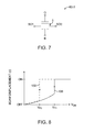
- FIG. 7 is a schematic diagram of a second type of relay switch 60-2.
- relay switch 60-2 may have source-drain terminals SD1 and SD2, gate terminal G, and body (or bulk) terminal B.
- Relay switch 60-2 may exhibit volatile behavior in which the state of switch 60-2 is lost if its gate and body terminals are not supplied with power.
- the amount by which the gate member of switch 60-2 is flexed towards the source-drain conductors is defined as beam displacement X.
- FIG. 8 is a plot of beam displacement versus gate-to-bulk voltage V GB .
- beam displacement X is minimal when V GB is less than pull-out threshold V PO (i.e., switch 60-2 will be turned off when V GB is less than V PO ).
- Beam displacement is maximized when V GB is greater than pull-in threshold VPI (i.e., switch 60-2 will be turned on when V GB is greater than V PI ).
- Switch 60-2 may exhibit a hysteresis behavior in which the on/off voltage transitions are different (e.g., the on/off transition requirements depend on the current state of switch 60-2).
- V PI is greater than V PO .
- FIG. 8 is merely illustrative and is not intended to limit the scope of the invention. If desired, V PI may be equal to V PO or less than V PO .
- FIG. 9 is a circuit diagram of a memory cell 18 that includes CMOS transistors and NEM relay switches in accordance with one embodiment of the present invention.
- cell 18 may include first and second cross-coupled inverting circuits INV1 and INV2.
- Inverting circuit INV1 may include relay switches 112 and 114 coupled in series between a first positive power supply line 108 (e.g., a power supply line on which positive power supply voltage Vcc1 is provided) and a first ground line 110 (e.g., a power supply line on which ground power supply voltage Vss1 is provided).
- Switches 112 and 114 may be volatile relay switches 60-2 of the typed described in connection with FIGS. 7 and 8 .
- the bulk terminal of switch 112 may be coupled to power supply line 108, whereas the bulk terminal of switch 110 may be coupled to power supply line 110.
- Inverting circuit INV2 may include p-channel pull-up transistor PU (e.g., a p-channel metal-oxide-semiconductor device) and n-channel pull-down transistor PD (e.g., an n-channel metal-oxide-semiconductor device) coupled in series between a second positive power supply line 104 (e.g., a power supply line on which positive power supply voltage Vcc2 is provided) and a second ground line 106 (e.g., a power supply line on which ground power supply voltage Vss2 is provided).
- a second positive power supply line 104 e.g., a power supply line on which positive power supply voltage Vcc2 is provided
- a second ground line 106 e.g., a power supply line on which ground power supply voltage Vss2 is provided.
- Vcc1/Vss1 associated with relay switches 112 and 114 may be equal or different in magnitude than Vcc2/Vss2 associated with CMOS transistors PU and PD (i.e., the relay devices and the CMOS devices are powered using separate power supply lines).
- Inverting circuits INV1 and INV2 may each have an input and an output.
- the output of INV1 may be coupled to the input of INV2 and may serve as a first data storage node nOUT for memory cell 18.
- the output of INV2 may be coupled to the input of INV1 and may serve as a second data storage node OUT for memory cell 18.
- Inverting circuits INV1 and INV2 cross-coupled in this way may be used as a latch to store true and complement versions of a single data bit at data storage nodes nOUT and OUT, respectively.
- cell 18 may be used to store a "0" (i.e., node OUT is low and node nOUT is high) or may be used to store a "1" (i.e., node OUT is high and node nOUT is low).
- This cross-coupled portion of cell 18 may therefore sometimes be referred to as a bistable memory element.
- a first access transistor such as transistor AC1 may be coupled between data storage node nOUT and a first data line (e.g., a data line on which true bit line signal BL is provided).
- a second access transistor such as transistor AC2 may be coupled between data storage node OUT and a second data line (e.g., a data line on which complement bit line signal nBL is provided).
- the gates of transistors AC1 and AC2 may be controlled using a corresponding word line signal WL.
- the access transistors may be used to read data from and write data into memory cell 18 (e.g., by asserting WL and biasing the bit line signals to appropriate voltage levels).
- Word line signal WL may sometimes be referred to as an address signal, whereas transistors AC1 and AC2 may sometimes be referred to as address transistors.
- Relay switches 112 and 114 in cell 18 of FIG. 9 may be formed in upper device portion 10-1 (see, e.g., FIG. 2 ), whereas transistors PU, PD, AC1, and AC2 are formed in lower device portion 10-2.
- the input and output of relay inverter circuit INV1 may be coupled down to transistor AC1 and CMOS inverter circuit INV2 through via paths 26 in dielectric stack 50.
- memory cell 18 of the type described in connection with FIG. 9 exhibits soft error upset immunity.
- a pulse of current I INJ_OUT being injected at node OUT (e.g., a current pulse peaking at 0.5 pA) and may cause the voltage at node OUT (V OUT ) to rise towards positive power supply voltage of 1.2 volts (as an example).
- V OUT may initiate turning on switch 114 and turning off switch 112.
- the amount of time it takes for the gate members of switches 112 and 114 to pull in or pull out e.g., time t0 to t2
- the duration of the injected noise current e.g., time t0 to t1
- node nOUT will remain high at t1.
- transistor PD is on and will serve to discharge V OUT back towards ground (i.e., cell 18 retains its stored value of "0").
- FIG. 11 shows another suitable arrangement of memory cell 18 in accordance with an embodiment of the present invention.
- cell 18 may include first and second cross-coupled inverting circuits INV1 and INV2.
- Inverting circuit INV1 may include relay switch 112 and n-channel transistor PD1 coupled in series between first positive power supply line 108 and a common ground line 107 (e.g., a power supply line on which ground voltage Vss is provided).
- Switch 112 may be relay switch 60-2 of the type described in connection with FIGS. 7 and 8 .
- the bulk terminal of switch 112 may be coupled to power supply line 108.
- Inverting circuit INV2 may include p-channel transistor PU and n-channel transistor PD2 coupled in series between second positive power supply line 104 and common ground line 107.
- Vcc1 associated with INV1 may be equal or different in magnitude than Vcc2 associated with INV2, but Vss may be supplied to both INV1 and INV2.
- INV1 and INV2 may receive different ground voltage signals from respective ground power supply lines.
- Inverting circuits INV1 and INV2 may each have an input and an output.
- the output of INVI may be coupled to the input of INV2 and may serve as a first data storage node nOUT for memory cell 18.
- the output of INV2 may be coupled to the input of INV1 and may serve as a second data storage node OUT for memory cell 18.
- First access transistor AC1 may be coupled between data storage node nOUT and a first data line
- second access transistor AC2 may be coupled between data storage node OUT and a second data line.
- the gates of transistors AC1 and AC2 may be controlled using corresponding word line signal WL.
- the access transistors may be used to read data from and write data into memory cell 18.
- Relay switch 112 in cell 18 of FIG. 11 may be formed in upper device portion 10-1 (see, e.g., FIG. 1 ), whereas transistors PD1, PD2, PU, AC1, and AC2 are formed in lower device portion 10-2 using standard CMOS fabrication techniques. Relay switch 112 may be coupled down to transistor AC1, PD1, and CMOS inverter circuit INV2 through via paths 26 in dielectric stack 50.
- Memory cell 18 of the type described in connection with FIG. 11 may also be used to exhibit soft error upset immunity.
- Memory cell 18 of the type described in connection with FIG. 11 may also be used to exhibit soft error upset immunity.
- Switch 112 remains on for the duration that V OUT is high because mechanical switching of relay devices is relatively slow compared to the electrical switching of CMOS transistors.
- V nOUT will stay relatively high (e.g., greater than 50% of Vcc1) because the on resistance of switch 112 is substantially lower than the on resistance of transistor PD1 (i.e., the mechanical conductance of relay devices is substantially higher than the electrical conductance of CMOS transistors).
- the effect of particle 200 dissipates, the high voltage on node nOUT enables transistor PD2 to discharge node OUT back towards ground.
- relay switches may be used in memory cells having less than six switching devices or more than six switching devices, in multiport memory cells, in memory cells with read buffer circuits, in memory cells having more than two cross-coupled inverting circuits, and in other types of memory elements.
- Memory cells that include relay devices may also exhibit reduced power consumption, because NEM relay devices exhibit substantially less source-drain leakage current relative to CMOS transistors.
Landscapes
- Engineering & Computer Science (AREA)
- Chemical & Material Sciences (AREA)
- Nanotechnology (AREA)
- Physics & Mathematics (AREA)
- Computer Hardware Design (AREA)
- Electromagnetism (AREA)
- Crystallography & Structural Chemistry (AREA)
- Theoretical Computer Science (AREA)
- Mathematical Physics (AREA)
- Static Random-Access Memory (AREA)
- Semiconductor Memories (AREA)
- Semiconductor Integrated Circuits (AREA)
- Design And Manufacture Of Integrated Circuits (AREA)
Applications Claiming Priority (1)
| Application Number | Priority Date | Filing Date | Title |
|---|---|---|---|
| US13/304,226 US8611137B2 (en) | 2011-11-23 | 2011-11-23 | Memory elements with relay devices |
Publications (2)
| Publication Number | Publication Date |
|---|---|
| EP2597679A2 true EP2597679A2 (de) | 2013-05-29 |
| EP2597679A3 EP2597679A3 (de) | 2018-02-28 |
Family
ID=47290646
Family Applications (1)
| Application Number | Title | Priority Date | Filing Date |
|---|---|---|---|
| EP12192532.5A Withdrawn EP2597679A3 (de) | 2011-11-23 | 2012-11-14 | Speicherelemente mit Relaisvorrichtungen |
Country Status (4)
| Country | Link |
|---|---|
| US (2) | US8611137B2 (de) |
| EP (1) | EP2597679A3 (de) |
| JP (2) | JP6504734B2 (de) |
| CN (1) | CN103137188B (de) |
Families Citing this family (9)
| Publication number | Priority date | Publication date | Assignee | Title |
|---|---|---|---|---|
| GB201215512D0 (en) | 2012-08-31 | 2012-10-17 | Ibm | Four terminal nano-electromechanical switch with a single mechanical contact |
| GB2505467A (en) * | 2012-08-31 | 2014-03-05 | Ibm | Dynamic logic gate comprising a nano-electro-mechanical switch |
| FR3009772B1 (fr) * | 2013-08-14 | 2015-09-25 | Commissariat Energie Atomique | Circuit logique a interrupteurs mecaniques a faible consommation |
| US9793080B2 (en) * | 2013-08-23 | 2017-10-17 | Inoso, Llc | Electromechanical power switch integrated circuits and devices and methods thereof |
| WO2016154521A1 (en) * | 2015-03-25 | 2016-09-29 | 3B Technologies, Inc. | Three dimensional integrated circuits employing thin film transistors |
| CN109378022B (zh) * | 2018-11-21 | 2023-08-22 | 灿芯半导体(上海)股份有限公司 | 一种多模式的onfi接口发送电路 |
| CN121122351A (zh) * | 2019-05-30 | 2025-12-12 | 国立研究开发法人科学技术振兴机构 | 电子电路 |
| US10971402B2 (en) | 2019-06-17 | 2021-04-06 | Taiwan Semiconductor Manufacturing Co., Ltd. | Semiconductor device including interface layer and method of fabricating thereof |
| CN112635472A (zh) * | 2020-12-08 | 2021-04-09 | 中国科学院微电子研究所 | 一种三维存算电路结构及其制备方法 |
Family Cites Families (39)
| Publication number | Priority date | Publication date | Assignee | Title |
|---|---|---|---|---|
| US3348206A (en) | 1963-09-25 | 1967-10-17 | Sperry Rand Corp | Relay storage units |
| DE3823186A1 (de) | 1988-07-08 | 1990-04-12 | Messerschmitt Boelkow Blohm | Elektromechanisches relais |
| JP3672954B2 (ja) * | 1994-12-26 | 2005-07-20 | 株式会社ルネサステクノロジ | 半導体記憶装置 |
| US5768186A (en) * | 1996-10-25 | 1998-06-16 | Ma; Yueh Yale | High density single poly metal-gate non-volatile memory cell |
| US6429492B1 (en) * | 1999-06-23 | 2002-08-06 | Bae Systems Information And Electronic Systems Integration, Inc. | Low-power CMOS device and logic gates/circuits therewith |
| JP2002222944A (ja) * | 2001-01-26 | 2002-08-09 | Kitakiyuushiyuu Techno Center:Kk | 半導体素子 |
| US6855988B2 (en) * | 2002-07-08 | 2005-02-15 | Viciciv Technology | Semiconductor switching devices |
| JP2004063605A (ja) * | 2002-07-26 | 2004-02-26 | Renesas Technology Corp | 半導体装置 |
| JP4343112B2 (ja) * | 2002-11-04 | 2009-10-14 | リサーチ イン モーション リミテッド | 無線通信装置バッテリ消費方法およびシステム |
| US7129925B2 (en) * | 2003-04-24 | 2006-10-31 | Hewlett-Packard Development Company, L.P. | Dynamic self-refresh display memory |
| EP1634296A4 (de) | 2003-06-09 | 2007-02-14 | Nantero Inc | Nichtflüchtige elektromechanische feldeffektbausteine und schaltungen damit und verfahren zu ihrer herstellung |
| US7583526B2 (en) * | 2003-08-13 | 2009-09-01 | Nantero, Inc. | Random access memory including nanotube switching elements |
| CA2535634A1 (en) * | 2003-08-13 | 2005-05-26 | Nantero, Inc | Nanotube-based switching elements with multiple controls and circuits made from same |
| US7190610B2 (en) * | 2004-06-16 | 2007-03-13 | Micron Technology, Inc. | Latch-up prevention for memory cells |
| US7060566B2 (en) * | 2004-06-22 | 2006-06-13 | Infineon Technologies Ag | Standby current reduction over a process window with a trimmable well bias |
| US7319253B2 (en) * | 2004-07-01 | 2008-01-15 | Altera Corporation | Integrated circuit structures for increasing resistance to single event upset |
| US7943418B2 (en) * | 2004-09-16 | 2011-05-17 | Etamota Corporation | Removing undesirable nanotubes during nanotube device fabrication |
| US7495952B2 (en) | 2005-07-13 | 2009-02-24 | Cornell Research Foundation, Inc. | Relay-connected semiconductor transistors |
| US7612424B1 (en) * | 2005-07-22 | 2009-11-03 | Northwestern University | Nanoelectromechanical bistable cantilever device |
| CN101273456B (zh) * | 2005-09-27 | 2012-04-18 | 康奈尔研究基金公司 | 形状记忆装置 |
| US7511532B2 (en) * | 2005-11-03 | 2009-03-31 | Cswitch Corp. | Reconfigurable logic structures |
| US7277351B2 (en) * | 2005-11-17 | 2007-10-02 | Altera Corporation | Programmable logic device memory elements with elevated power supply levels |
| US8258899B2 (en) * | 2006-11-14 | 2012-09-04 | California Institute Of Technology | Nano-electro-mechanical systems switches |
| US20090102289A1 (en) * | 2007-10-18 | 2009-04-23 | Aipperspach Anthony G | Techniques for Selecting a Voltage Source From Multiple Voltage Sources |
| KR100884450B1 (ko) * | 2007-11-08 | 2009-02-19 | 삼성모바일디스플레이주식회사 | 유기전계발광 표시장치 |
| US7911826B1 (en) * | 2008-03-27 | 2011-03-22 | Altera Corporation | Integrated circuits with clearable memory elements |
| US7612270B1 (en) * | 2008-04-09 | 2009-11-03 | International Business Machines Corporation | Nanoelectromechanical digital inverter |
| US8289755B1 (en) * | 2008-10-01 | 2012-10-16 | Altera Corporation | Volatile memory elements with soft error upset immunity |
| JP2010129371A (ja) * | 2008-11-27 | 2010-06-10 | Toshiba Corp | スイッチ及びesd保護素子 |
| KR101529052B1 (ko) * | 2009-01-30 | 2015-06-16 | 삼성전자주식회사 | 풀 씨모스 에스 램 |
| KR20100094192A (ko) * | 2009-02-18 | 2010-08-26 | 삼성전자주식회사 | 탄소나노튜브 박막을 이용한 에스램 |
| US8081503B1 (en) * | 2009-02-27 | 2011-12-20 | Altera Corporation | Volatile memory elements with minimized area and leakage current |
| US7872903B2 (en) * | 2009-03-19 | 2011-01-18 | Altera Corporation | Volatile memory elements with soft error upset immunity |
| US8012785B2 (en) * | 2009-04-24 | 2011-09-06 | Taiwan Semiconductor Manufacturing Company, Ltd. | Method of fabricating an integrated CMOS-MEMS device |
| US8779886B2 (en) * | 2009-11-30 | 2014-07-15 | General Electric Company | Switch structures |
| US8826529B2 (en) * | 2009-09-23 | 2014-09-09 | General Electric Company | Method of forming a micro-electromechanical system device |
| US8563885B2 (en) * | 2009-11-11 | 2013-10-22 | University Of Utah Research Foundation | Cantilevered beam NEMS switch |
| US20120043905A1 (en) * | 2010-08-18 | 2012-02-23 | Lutron Electronics Co., Inc. | Method of Controlling an Operating Frequency of an Inverter Circuit in an Electronic Dimming Ballast |
| US9385058B1 (en) * | 2012-12-29 | 2016-07-05 | Monolithic 3D Inc. | Semiconductor device and structure |
-
2011
- 2011-11-23 US US13/304,226 patent/US8611137B2/en not_active Expired - Fee Related
-
2012
- 2012-11-08 JP JP2012246307A patent/JP6504734B2/ja active Active
- 2012-11-14 CN CN201210458102.9A patent/CN103137188B/zh active Active
- 2012-11-14 EP EP12192532.5A patent/EP2597679A3/de not_active Withdrawn
-
2013
- 2013-11-27 US US14/092,298 patent/US9520182B2/en active Active
-
2017
- 2017-07-27 JP JP2017145414A patent/JP2017228782A/ja active Pending
Non-Patent Citations (1)
| Title |
|---|
| None |
Also Published As
| Publication number | Publication date |
|---|---|
| EP2597679A3 (de) | 2018-02-28 |
| US20130127494A1 (en) | 2013-05-23 |
| JP2013110409A (ja) | 2013-06-06 |
| JP2017228782A (ja) | 2017-12-28 |
| US9520182B2 (en) | 2016-12-13 |
| US20140085967A1 (en) | 2014-03-27 |
| CN103137188B (zh) | 2017-09-19 |
| CN103137188A (zh) | 2013-06-05 |
| US8611137B2 (en) | 2013-12-17 |
| JP6504734B2 (ja) | 2019-04-24 |
Similar Documents
| Publication | Publication Date | Title |
|---|---|---|
| US9520182B2 (en) | Memory elements with relay devices | |
| US7920410B1 (en) | Memory elements with increased write margin and soft error upset immunity | |
| US9344067B1 (en) | Dual interlocked cell (DICE) storage element with reduced charge sharing | |
| US6058041A (en) | SEU hardening circuit | |
| CN102918598B (zh) | 具有软错误翻转免疫性的存储器元件 | |
| CN103871460B (zh) | 具有叠置的上拉装置的存储器元件 | |
| US8289755B1 (en) | Volatile memory elements with soft error upset immunity | |
| CN102203867B (zh) | 具有软错误翻转抗扰性的易失性存储器元件 | |
| US20100238715A1 (en) | Volatile memory elements with soft error upset immunity | |
| CN109215708B (zh) | 具有可编程非易失性电阻开关元件的集成电路 | |
| US8476951B2 (en) | Latch circuit with single node single-event-upset immunity | |
| US8750026B1 (en) | Integrated circuits with asymmetric and stacked transistors | |
| US9496268B2 (en) | Integrated circuits with asymmetric and stacked transistors | |
| US8797790B1 (en) | Memory elements with soft error upset immunity | |
| WO2013130966A2 (en) | Fault tolerant static random-access memory | |
| US12294363B2 (en) | Circuit for mitigating single-event-transients | |
| US10079602B1 (en) | Unipolar latched logic circuits | |
| US6724676B1 (en) | Soft error improvement for latches | |
| US20250095761A1 (en) | High voltage transfer device and a memory device including the same | |
| US10242732B2 (en) | Memory elements with soft-error-upset (SEU) immunity using parasitic components | |
| Li et al. | Laser Study for DICE-based Registers in a Commercial 130nm Process Technology |
Legal Events
| Date | Code | Title | Description |
|---|---|---|---|
| PUAI | Public reference made under article 153(3) epc to a published international application that has entered the european phase |
Free format text: ORIGINAL CODE: 0009012 |
|
| AK | Designated contracting states |
Kind code of ref document: A2 Designated state(s): AL AT BE BG CH CY CZ DE DK EE ES FI FR GB GR HR HU IE IS IT LI LT LU LV MC MK MT NL NO PL PT RO RS SE SI SK SM TR |
|
| AX | Request for extension of the european patent |
Extension state: BA ME |
|
| RIC1 | Information provided on ipc code assigned before grant |
Ipc: G11C 11/52 20060101AFI20171020BHEP Ipc: H01H 1/00 20060101ALN20171020BHEP Ipc: H01L 27/11 20060101ALN20171020BHEP Ipc: H01H 1/20 20060101ALN20171020BHEP Ipc: G11C 23/00 20060101ALI20171020BHEP Ipc: H01L 27/10 20060101ALI20171020BHEP Ipc: B82Y 10/00 20110101ALI20171020BHEP Ipc: G11C 13/02 20060101ALI20171020BHEP Ipc: H01H 59/00 20060101ALI20171020BHEP |
|
| PUAL | Search report despatched |
Free format text: ORIGINAL CODE: 0009013 |
|
| AK | Designated contracting states |
Kind code of ref document: A3 Designated state(s): AL AT BE BG CH CY CZ DE DK EE ES FI FR GB GR HR HU IE IS IT LI LT LU LV MC MK MT NL NO PL PT RO RS SE SI SK SM TR |
|
| AX | Request for extension of the european patent |
Extension state: BA ME |
|
| RIC1 | Information provided on ipc code assigned before grant |
Ipc: G11C 13/02 20060101ALI20180119BHEP Ipc: H01L 27/11 20060101ALN20180119BHEP Ipc: H01L 27/10 20060101ALI20180119BHEP Ipc: B82Y 10/00 20110101ALI20180119BHEP Ipc: H01H 59/00 20060101ALI20180119BHEP Ipc: G11C 11/52 20060101AFI20180119BHEP Ipc: H01H 1/00 20060101ALN20180119BHEP Ipc: G11C 23/00 20060101ALI20180119BHEP Ipc: H01H 1/20 20060101ALN20180119BHEP |
|
| 17P | Request for examination filed |
Effective date: 20180817 |
|
| RBV | Designated contracting states (corrected) |
Designated state(s): AL AT BE BG CH CY CZ DE DK EE ES FI FR GB GR HR HU IE IS IT LI LT LU LV MC MK MT NL NO PL PT RO RS SE SI SK SM TR |
|
| STAA | Information on the status of an ep patent application or granted ep patent |
Free format text: STATUS: THE APPLICATION HAS BEEN WITHDRAWN |
|
| 18W | Application withdrawn |
Effective date: 20200825 |