EP2579293B1 - Ionenmobilitätsröhre - Google Patents
Ionenmobilitätsröhre Download PDFInfo
- Publication number
- EP2579293B1 EP2579293B1 EP11803093.1A EP11803093A EP2579293B1 EP 2579293 B1 EP2579293 B1 EP 2579293B1 EP 11803093 A EP11803093 A EP 11803093A EP 2579293 B1 EP2579293 B1 EP 2579293B1
- Authority
- EP
- European Patent Office
- Prior art keywords
- metal electrode
- insulator
- ion mobility
- electrode sheets
- mobility tube
- Prior art date
- Legal status (The legal status is an assumption and is not a legal conclusion. Google has not performed a legal analysis and makes no representation as to the accuracy of the status listed.)
- Not-in-force
Links
Images



Classifications
-
- G—PHYSICS
- G01—MEASURING; TESTING
- G01N—INVESTIGATING OR ANALYSING MATERIALS BY DETERMINING THEIR CHEMICAL OR PHYSICAL PROPERTIES
- G01N27/00—Investigating or analysing materials by the use of electric, electrochemical, or magnetic means
- G01N27/62—Investigating or analysing materials by the use of electric, electrochemical, or magnetic means by investigating the ionisation of gases, e.g. aerosols; by investigating electric discharges, e.g. emission of cathode
- G01N27/622—Ion mobility spectrometry
Definitions
- the present invention relates generally to a detection apparatus based on ion mobility principles for trace detection, and in particular to an ion mobility tube.
- the ion mobility tube is a core part of a detection apparatus based on the ion mobility principles. It generally comprises an ionization source chamber, an ion door, a mobility region, a constraining grid, and a Faraday disk.
- the above components of a conventional ion mobility tube are formed by means of separate metal electrode sheets.
- the electrode sheets are separated from each other by insulating material.
- the metal electrode sheets are connected to an external cable or separate divider resistors are welded between the metal electrode sheets, or divider resistors are disposed outside the ion mobility tube.
- Such an ion mobility tube has a complicated structure with many lead wires, and cannot be easily detached since two electrode sheets are welded to each other through wires or electronic elements.
- all the structures such as the ion door and the constraining grid are made of thin net-shaped or wire-shaped metal and thus have a bad strength in the conventional ion mobility tube. Change in performance caused by deformation is considerable, therefore accuracy of detection of the ion mobility tube is degraded.
- PLUMLEE D ET AL "Development of a micro-nozzle and ion mobility spectrometer in LTCC", MICROELECTRONICS AND ELECTRON DEVICES, 2004 IEEE WORKSHOP ON BOISE, ID, USA 16 APRIL 2004, PISCATAWAY, NJ, USA, IEEE, US, 1 January 2004 (2004-01-01), pages 95-98, XP010705323, DOI: 10.1109/WMED.2004.1297362 ISBN: 978-0-7803-8369-2 describes an ion mobility spectrometer (IMS) for permanent deployment below ground to continuously analyze groundwater pollutants. Each segment is constructed of multiple layers of green tape. Five Kovar inserts are embedded in the device to function as ion gates. A reduction in size, hermeticity and system integration is possible by the use of LTCC packaging technology.
- IMS ion mobility spectrometer
- an object of the present invention is to provide an ion mobility tube which has a simplified structure and can be conveniently manufactured and detached.
- An ion mobility tube comprises an ionization source chamber having a center ionization source chamber hole, an ion door, a mobility region unit having a center mobility tube chamber, a constraining grid, and a Faraday disk, the ionization source chamber, the ion door, the mobility region unit, the constraining grid, and the Faraday disk are stacked together in sequence in a front-rear direction, wherein the mobility region unit comprises a first insulator and first metal electrode sheets concentrically fixed to a front surface and a back surface of the first insulator respectively.
- the mobility region unit comprises the first insulator and the first metal electrode sheets which are integral. Therefore, the mobility tube is advantageous in simplified manufacturing process, and convenient for detachment and assembly.
- the ion mobility tube according to an embodiment of the present invention further has the following additional technical features.
- the first insulator is formed with a first electronic element accommodating hole located on radial outsides of the first metal electrode sheets.
- the first insulator is further formed with a first wiring hole located on the radial outsides of the first metal electrode sheets.
- the ionization source chamber comprises a second insulator and second metal electrode sheets concentrically fixed to a front surface and a back surface of the second insulator respectively and connected to each other.
- the second insulator is formed with a second electronic element accommodating hole located on radial outsides of the second metal electrode sheets.
- the second insulator is further formed with a second wiring hole located on the radial outsides of the second metal electrode sheets.
- the ionization source chamber is formed with a second electric via hole penetrating through the second insulator and the second metal electrode sheets.
- the ion door comprises a third insulator and third metal electrode sheets concentrically fixed to a front surface and a back surface of the third insulator respectively.
- the third insulator is formed with a third electronic element accommodating hole located on radial outsides of the third metal electrode sheets.
- the third insulator is formed with a third wiring hole located on the radial outsides of the third metal electrode sheets.
- the constraining grid comprises a fourth insulator, and a fourth front metal electrode sheet and a fourth back metal electrode sheet concentrically fixed to a front surface and a back surface of the fourth insulator respectively and connected to each other, wherein the fourth back metal electrode sheet is annular in shape.
- the fourth insulator is formed with a fourth electronic element accommodating hole located on radial outsides of the fourth front metal electrode sheet and the fourth back metal electrode sheet.
- the fourth insulator is formed with a fourth wiring hole located on the radial outsides of the fourth front metal electrode sheet and the fourth back metal electrode sheet.
- the constraining grid is formed with a fourth electronic via hole penetrating through the fourth insulator to connect the fourth front metal electrode sheet and the fourth back metal electrode sheet.
- the Faraday disk comprises a fifth insulator and fifth metal electrode sheets concentrically fixed to a front surface and a back surface of the fifth insulator respectively and connected to each other.
- the fifth insulator is formed with a fifth electronic element accommodating hole located on radial outsides of the fifth metal electrode sheets.
- the Faraday disk further comprises annular metal electrode sheets concentrically fixed to the front surface and the back surface of the fifth insulator respectively, fitted over the radial outsides of the fifth metal electrode sheets respectively, and connected to each other, wherein the fifth electronic element accommodating hole is located on radial outsides of the annular metal electrode sheets.
- the fifth insulator is further formed with a fifth wiring hole located on the radial outsides of the annular metal electrode sheets.
- the fifth insulator is formed with a ventilation hole located inside the annular metal electrode sheets and outside the fifth metal electrode sheets.
- the Faraday disk is formed with a fifth electric via hole for connecting the annular metal electrode sheets.
- the ion mobility tube further comprises a Faraday disk rear cover ring and a Faraday disk rear cover plate stacked in sequence behind the Faraday disk, the Faraday disk rear cover plate comprises a sixth insulator and sixth metal electrode sheets concentrically fixed to a front surface and a back surface of the sixth insulator respectively and connected to each other, and the Faraday disk rear cover ring comprises a seventh insulator having a seventh center hole and seventh annular metal electrode sheets concentrically fixed to a front surface and a back surface of the seventh insulator respectively.
- the sixth insulator is formed with sixth wiring holes respectively located on the radial outsides of the sixth metal electrode sheets
- the seventh insulator is formed with seventh wiring holes respectively located on the radial outsides of the seventh annular metal electrode sheets.
- the Faraday disk rear cover plate is formed with sixth electric via holes respectively penetrating through the sixth insulator and the sixth metal electrode sheets.
- a gas nozzle is mounted on a back surface of the Faraday disk rear cover plate.
- the ionization source chamber, the ion door, the mobility region unit, the constraining grid, the Faraday disk, and the Faraday disk rear cover plate are formed with mounting holes respectively, and stacked together by means of a bolt that passes through the mounting holes.
- the first insulator is ceramic, and the first metal electrode sheets are formed on the first insulator by corrosion, electroplating, deposition, or spray painting, respectively.
- orientations or positional relationships indicated by the terms such as “front”, “back”, “left”, “right”, “radial” “axial”, and “rear” are based on orientations or positional relationships shown in the accompanying drawings, are merely used to facilitate the description of the present invention, but do not require that the present invention should be configured and operated in a particular orientation. Therefore, the orientations or positional relationships should not be construed to limit the present invention.
- the ion mobility tube comprises an ionization source chamber 1, an ion door 2, a mobility region unit 3, a constraining grid 4, and a Faraday disk 5.
- the ion mobility tube further comprises a Faraday disk rear cover plate 6.
- the ionization source chamber 1, the ion door 2, the mobility region unit 3, the constraining grid 4, the Faraday disk 5, a Faraday disk rear cover ring 7, and the Faraday disk rear cover plate 6 are stacked together in sequence in a front-rear direction (a right-left direction in FIG. 1 ).
- the ionization source chamber 1, the ion door 2, the mobility region unit 3, the constraining grid 4, the Faraday disk 5, and the Faraday disk rear cover plate 6 are formed with mounting holes at upper left corners and lower right corners, respectively, and bolts 80 pass through the mounting holes to assemble them together in sequence in the front-rear direction.
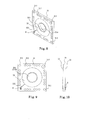
- the mobility region unit 3 has a center mobility tube chamber 314, and comprises a first insulator 31 and first metal electrode sheets 32 concentrically fixed to a front surface (a left surface in FIG. 10 ) and a back surface (a right surface in FIG. 10 ) of the first insulator 31 respectively.
- the first metal electrode sheets 32 have first metal electrode sheet center holes 321 corresponding to the center mobility tube chamber 314.
- the first metal electrode sheets 32 may be connected to each other through an electronic element 8.
- the first metal electrode sheets 32 are connected to each other through a resistor.
- the electronic element 8 connects the first metal electrode sheets 32 on the front and back surfaces through lead wires 322 led out from the first metal electrode sheets 32 on the front and back surfaces, respectively.
- the first insulator 31 is ceramic and thus has high-temperature resistance and high-voltage resistance
- the first metal electrode sheets 32 may be formed on the first insulator 31 by corrosion, electroplating, deposition, or spray painting so that the insulator 31 and the first metal electrode sheets 32 on the front and back surfaces constitute a single integral unit.
- the present invention is not limited to this.
- the first insulator 31 may also be made of the same material as a common circuit board, and the first metal electrode sheets 32 are formed on the first insulator 31 as a circuit is printed on a circuit board.
- the first insulator 31 and the first metal electrode sheets 32 are generally square in shape, but the present invention is not limited to this.
- the mobility region unit comprises the first insulator 31 and the first metal electrode sheets 32 which are integral. Therefore, the mobility region unit can be formed directly by series connection so long as mutual metal portions of the mobility region units between the mobility region units are brought into contact with each other. Hence, assembly and detachment are simply carried out and cost thereof is reduced.
- a mobility region of the mobility tube may comprise a plurality of the mobility region units 3.
- the mobility region comprises a plurality of the first insulators 31 which are stacked together and of which the front and back surfaces are fixed with the first metal electrode sheets 32 respectively, as shown in FIG. 11 .
- a specific number of the mobility region units 3 may be selected according to specific application. Therefore, a length of the mobility region of the mobility tube can be conveniently adjusted.
- the first insulator 31 is formed with a first electronic element accommodating hole 313 located on radial outsides of the first metal electrode sheets 32.
- the first electronic element accommodating hole 313 is formed at an upper right corner of the first insulator 31.
- the first electronic element accommodating hole 313 is used to accommodate the electronic element 8 welded to the adjacent mobility region unit 3.
- the first electronic element accommodating hole 313 in one of the mobility region units 3 is opposite to the electronic element 8 on the one of the mobility region units 3. Therefore, the first electronic element accommodating hole 313 in one of the mobility region units 3 is opposite to the first electronic element accommodating hole 313 in adjacent one of the mobility region units 3.
- the electronic element on one of the mobility region units 3 is accommodated in the first electronic element accommodating hole 313 in adjacent one of the mobility region units 3. Therefore, it is not necessary to lead out lead wires for connection to an external electronic element from the first metal electrode sheets 32. As a result, lead wires of the mobility region unit 3 are decreased, the structure thereof is simplified. It is convenient to carry out manufacture and assembly of the tube, the appearance thereof is neat, and reliability of connection of the electronic elements is improved.
- the first insulator 31 is further formed with a first wiring hole 312 which is located on the radial outsides of the first metal electrode sheets 32, and through which a cable passes, so that it is not necessary to expose the cable of the mobility tube to an outside of the mobility tube, thereby ensuring reliability of connection, neat appearance, and convenient connection.
- the first wiring hole 312 is formed at a peripheral edge of the first insulator 31.
- the first insulator 31 is formed with mounting holes 311 at an upper left corner and a lower right corner, respectively, and the bolts 80 pass through the mounting holes to stack the mobility region units 3 and the other components of the mobility tube together in sequence to form the ion mobility tube.
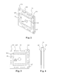
- the ionization source chamber 1 of the ion mobility tube according to an embodiment of the present invention will now be described with reference to FIGS. 2-4 .
- the ionization source chamber 1 has a ionization source chamber center hole, and the ionization source chamber 1 comprises a second insulator 11 and second metal electrode sheets 12 concentrically fixed to a front surface (a left surface in FIG. 4 ) and a back surface (a right surface in FIG. 4 ) of the second insulator 11 respectively and connected to each other.
- the insulator 11 has a second insulator center hole 114, and accordingly the second metal electrode sheets 12 have second metal electrode sheet center holes 121.
- the second insulator 11 is provided with mounting holes 113 at an upper left corner and a lower right corner, respectively, and the bolts 80 pass through the mounting holes to stack the ionization source chamber 3 and the other components of the mobility tube together.
- the second insulator 11 may also be ceramic, and the second metal electrode sheets 12 may be formed on the second insulator 12 by corrosion, electroplating, deposition, or spray painting.
- the second insulator 11 may also be made of the same material as a common circuit board, and the second metal electrode sheets 12 are formed on the second insulator 11 as a circuit is printed on a circuit board.
- the second insulator 11 is formed with a second electronic element accommodating hole 112 located on radial outsides of the second metal electrode sheets 12. More specifically, the second electronic element accommodating hole 112 is formed at an upper right corner of the second insulator 11 to accommodate the electronic element.
- the second insulator 11 and the second metal electrode sheets 12 have a generally square shape in the example shown in FIGS. 2 and 3 , but the present invention is not limited to this.
- the second insulator 11 is further formed with a second wiring hole 111 located on the radial outsides of the second metal electrode sheets 12.
- a cable passes through the second wiring hole 111 which is similar to the first wiring hole 312. After the mobility tube is assembled, the second wiring hole 111 is aligned with the first wiring hole 312.
- the ionization source chamber 1 is formed with a second electric via hole 122 penetrating through the second insulator 11 and the second metal electrode sheets 12.
- the second electric via hole 122 is used to connect the second metal electrode sheets 12 located on the front and back surfaces of the second insulator 11. It should be appreciated that connection of the second metal electrode sheets 12 on the front and back surfaces of the second insulator 11 is not limited to the connection performed by the second electric via hole 122.
- the second metal electrode sheets 12 on both sides may also be connected through metal disposed within the center holes of the second insulator 11 and the second metal electrode sheets 12.
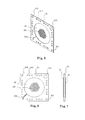
- the ion door 2 of the ion mobility tube according to an embodiment of the present invention will now be described with reference to FIGS. 5-7 .
- the ion door 2 comprises a third insulator 21 and third metal electrode sheets 22 concentrically fixed to a front surface and a back surface of the third insulator 21 respectively.
- the third insulator 21 may be e.g. ceramic, and the third metal electrode sheets 22 may be fixed to the front surface and the back surface of the third insulator 21 in the above appropriate manners.
- the third insulator 21 is formed with a third electronic element accommodating hole 213 located on radial outsides of the third metal electrode sheets 22.
- the third electronic element accommodating hole 213 is formed at an upper right corner of the third insulator 21 to accommodate the electronic element.
- the electronic element is connected to the third metal electrode sheets 22 on the front and back surfaces through lead wires 223 led out from the third metal electrode sheets 22 on the front and back surfaces of the third insulator 21, respectively, so as to connect the two third metal electrode sheets 22 on the front and back surfaces.
- the third insulator 21 is formed with mounting holes 211 at an upper left corner and a lower right corner, respectively, and the bolts 80 pass through the mounting holes.
- the third insulator 21 is formed with a third wiring hole 212 located on the radial outsides of the third metal electrode sheets 22.A cable passes through the third wiring hole 212.
- the third metal electrode sheets 22 on the front and back surfaces of the third insulator 21 are formed with ion passage holes 221 and accordingly the third insulator 21 is also formed with a ion passage hole aligned with the ion passage holes 221 so that ions may pass through the ion passage holes, which is similar to prior art and is not further described in detail.
- the constraining grid 4 of the ion mobility tube according to an embodiment of the present invention will now be described with reference to FIGS. 13 and 14 .
- the constraining grid 4 comprises a fourth insulator 41, and a fourth front metal electrode sheet 42 and a fourth back metal electrode sheet 43 concentrically fixed to a front surface and a back surface of the fourth insulator 41 respectively and connected to each other.
- the fourth back metal electrode sheet 43 is annular in shape.
- the fourth insulator 41 is formed with a fourth electronic element accommodating hole 413 located on radial outsides of the fourth front metal electrode sheet 42 and the fourth back metal electrode sheet 43 to accommodate the electronic element.
- the fourth insulator 41 is formed with a fourth wiring hole 412 located on the radial outsides of the fourth front metal electrode sheet 42 and the fourth back metal electrode sheet 43.
- the cable passes through the fourth wiring hole 412.
- the fourth insulator 41 is further formed with mounting holes 411, and the bolts 80 pass through the mounting holes 411.
- the fourth insulator 41 is formed with a fourth electronic via hole 421 penetrating through the fourth insulator 41 to connect the fourth front metal electrode sheet 42 and the fourth back metal electrode sheet 43. Accordingly, the fourth insulator 41 may be formed with a corresponding via hole 414.
- the fourth electronic via hole 421 is used to connect the fourth front metal electrode sheet 42 and the fourth back metal electrode sheet 43, but the present invention is not limited to this.
- the fourth front metal electrode sheet 42 is formed with an ion passage hole 422 and accordingly the fourth insulator 4 is formed with a passage hole 415 so that ions pass through the passage holes, which is similar to prior art and is not further described in detail.
- the fourth front metal electrode sheet 42 is generally circular in shape, and the ion passage hole 422 is formed in a center portion of the fourth front metal electrode sheet.
- the fourth back metal electrode sheet 43 is annular in shape, and the ion passage hole 422 and the passage hole 415 are formed inside a center hole of the fourth back metal electrode sheet 43.
- the fourth insulator 41 may also be ceramic, and the fourth front metal electrode sheet 42 and the fourth back metal electrode sheet 43 may be formed and fixed on the fourth insulator 41 in the above appropriate manners.
- the Faraday disk 5 of the ion mobility tube according to an embodiment of the present invention will now be described with reference to FIGS. 15 and 16 .
- the Faraday disk 5 comprises a fifth insulator 51 and fifth metal electrode sheets 53 concentrically fixed to a front surface and a back surface of the fifth insulator 51 respectively and connected to each other.
- the fifth insulator 51 is formed with a fifth electronic element accommodating hole 513 located on radial outsides of the fifth metal electrode sheets 53 to accommodate the electronic element.
- the fifth insulator 51 is further formed with mounting holes 511, and the bolts 80 pass through the mounting holes.
- the Faraday disk 5 further comprises annular metal electrode sheets 53 concentrically fixed to the front surface and the back surface of the fifth insulator 51 respectively, fitted over the radial outsides of the fifth metal electrode sheets 53 respectively, and connected to each other.
- the fifth electronic element accommodating hole 513 is located on radial outsides of the annular metal electrode sheets 52.
- a fifth wiring hole 512 is formed in the fifth insulator 51 on the radial outsides of the annular metal electrode sheets 52.
- the cable passes through the fifth wiring hole 512.
- the Faraday disk 5 may also be formed with a fifth electric via hole 521 for connecting the annular metal electrode sheets 52.
- the fifth metal electrode sheets 53 may be connected to each other through a center hole 531, and accordingly a center hole 515 is formed in the fifth insulator 51.
- the fifth insulator 51 is formed with a first ventilation hole 514 between the fifth metal electrode sheets 53 and the annular metal electrode sheets 52 to introduce air into the mobility tube.
- the fifth insulator 51 may be ceramic, and the fifth metal electrode sheets 53 and the annular metal electrode sheets 52 may be formed and fixed on the fifth insulator 51 in the above appropriate manners.
- the Faraday disk rear cover ring 7 and Faraday disk rear cover plate 6 of the ion mobility tube will now be described with reference to FIGS. 17 and 18 .
- the Faraday disk rear cover plate 6 comprises a sixth insulator 61 and sixth metal electrode sheets 62 concentrically fixed to a front surface and a back surface of the sixth insulator 61 respectively and connected to each other.
- the sixth insulator 61 is formed with mounting holes 611, and the bolts 80 pass through the mounting holes 611.
- the sixth insulator 61 is formed with sixth wiring holes 612 respectively located on radial outsides of the sixth metal electrode sheets 62. The cable passes through the sixth wiring holes.
- the Faraday disk rear cover plate 6 is formed with sixth electric via holes 621 (the corresponding electric via hole in the sixth insulator 61 is indicated by 613) respectively penetrating through the sixth insulator 61 and the sixth metal electrode sheets 62 to connect the sixth metal electrode sheets 62 on both sides of the sixth insulator 61.
- a spring 9 may be mounted at a center portion of the sixth insulator 61 to be in contact with the fifth metal electrode sheets 53 of the Faraday disk 5.
- a gas nozzle is mounted on a back surface of the six insulator 61 to ventilate an inside of the mobility tube through the ventilation hole.
- the sixth insulator 61 may also be ceramic, and the sixth metal electrode sheets 62 may be formed and fixed on the front surface and the back surface of the sixth insulator 61 in the above appropriate manners.
- the Faraday disk rear cover ring 7 is disposed between the Faraday disk rear cover plate 6 and the Faraday disk 5 to provide the spring 9 with a stroke space so as to ensure good contact.
- the Faraday disk rear cover ring 7 comprises a seventh insulator 71 having a center hole 714, and seventh annular metal electrode sheets 72 disposed on a front surface and a back surface of the seventh insulator respectively.
- Mounting holes 711 is formed through the seventh insulator 71 on radial outsides of the seventh annular metal electrode sheets 72, and the bolts 80 pass through the mounting holes.
- the mounting holes 711 are formed at an upper left corner and a lower right corner of the seventh insulator 71.
- the seventh insulator 71 is further formed with a seventh wiring hole 712 located on the radial outsides of the seventh annular metal electrode sheets 72. The cable passes through the seventh wiring hole.
- the ionization source chamber 1, the ion door 2, the mobility region unit 3, the constraining grid 4, the Faraday disk 5, and the Faraday disk rear cover plate 6 may be stacked together in sequence by means of the bolts 80, and each of the above members is an integral unit composed of an insulator and metal electrode sheets, the electronic elements may be accommodated in the corresponding electronic element accommodating holes, and thus external lead wires and externally linked electronic elements are not needed and the cable can pass through the mobility tube through the wiring holes. Therefore, the mobility tube according to the present invention is advantageous in simplified manufacturing, convenient for assembly and detachment, and has a neat appearance, high reliability and accuracy of detection.
Landscapes
- Chemical & Material Sciences (AREA)
- Physics & Mathematics (AREA)
- Biochemistry (AREA)
- General Health & Medical Sciences (AREA)
- Electrochemistry (AREA)
- Health & Medical Sciences (AREA)
- Life Sciences & Earth Sciences (AREA)
- Analytical Chemistry (AREA)
- Spectroscopy & Molecular Physics (AREA)
- Chemical Kinetics & Catalysis (AREA)
- General Physics & Mathematics (AREA)
- Immunology (AREA)
- Pathology (AREA)
- Measurement Of Radiation (AREA)
- Other Investigation Or Analysis Of Materials By Electrical Means (AREA)
- Electron Tubes For Measurement (AREA)
- Plasma Technology (AREA)
- Electron Sources, Ion Sources (AREA)
Claims (22)
- Eine Ionenbeweglichkeitsröhre, die folgende Merkmale aufweist:eine Ionisierungsquellenkammer (1) mit einem mittleren Ionisierungsquellenkammerloch, eine Ionentür (2), eine Beweglichkeitsregionseinheit (3) mit einer mittleren Beweglichkeitsröhrenkammer, ein Begrenzungsgitter (4) und eine Faradaysche Scheibe (5), und die Ionisierungsquellenkammer, die Ionentür, die Beweglichkeitsregionseinheit, das Begrenzungsgitter und die Faradaysche Scheibe sind hintereinander in einer Richtung von vorne nach hinten gestapelt, dadurch gekennzeichnet, dass die Beweglichkeitsregionseinheit einen ersten Isolator (31) und erste Metallelektrodenlagen (32) aufweist, die konzentrisch an einer Vorderoberfläche beziehungsweise einer Rückoberfläche des ersten Isolators fixiert sind,der erste Isolator (31) mit einem ersten Elektronikelementaufnahmeloch (331) gebildet ist, das an radialen Außenseiten der ersten Metallelektrodenlagen (32) angeordnet ist, die Ionenbeweglichkeitsröhre ferner ein Elektronikelement (8) aufweist, und das Elektronikelement (8) in dem ersten Elektronikelementaufnahmeloch angeordnet ist, unddie Ionisierungsquellenkammer (1), die Ionentür (2), die Beweglichkeitsregionseinheit (3), das Begrenzungsgitter (4) und die Faradaysche Scheibe (5) lösbar gestapelt sind.
- Die Ionenbeweglichkeitsröhre gemäß Anspruch 1, dadurch gekennzeichnet, dass der erste Isolator (31) ferner mit einem ersten Verdrahtungsloch (312) gebildet ist, das an den radialen Außenseiten der ersten Metallelektrodenlagen (32) angeordnet ist, und ein Kabel der Ionenbeweglichkeitsröhre durch das erste Verdrahtungsloch verläuft.
- Die Ionenbeweglichkeitsröhre gemäß Anspruch 1, dadurch gekennzeichnet, dass die Ionisierungsquellenkammer (1) einen zweiten Isolator (11) und zweite Metallelektrodenlagen (12) aufweist, die konzentrisch an einer Vorderoberfläche beziehungsweise einer Rückoberfläche des zweiten Isolators fixiert sind und miteinander verbunden sind.
- Die Ionenbeweglichkeitsröhre gemäß Anspruch 3, dadurch gekennzeichnet, dass der zweite Isolator (11) mit einem zweiten Elektronikelementaufnahmeloch (112) gebildet ist, das an radialen Außenseiten der zweiten Metallelektrodenlagen (12) angeordnet ist und ein Elektronikelement der Ionenbeweglichkeitsröhre aufnimmt.
- Die Ionenbeweglichkeitsröhre gemäß Anspruch 4, dadurch gekennzeichnet, dass der zweite Isolator (11) ferner mit einem zweiten Verdrahtungsloch (111) gebildet ist, das an den radialen Außenseiten der zweiten Metallelektrodenlagen (12) angeordnet ist, und ein Kabel der Ionenbeweglichkeitsröhre durch das zweite Verdrahtungsloch verläuft.
- Die Ionenbeweglichkeitsröhre gemäß Anspruch 5, dadurch gekennzeichnet, dass die Ionisierungsquellenkammer (1) mit einem zweiten elektrischen Durchgangsloch (122) gebildet ist, das durch den zweiten Isolator (11) und die zweite Metallelektrodenlagen (12) dringt, und das zweite elektrische Durchgangsloch (122) die zweiten Metallelektrodenlagen (12) verbindet.
- Die Ionenbeweglichkeitsröhre gemäß Anspruch 1, dadurch gekennzeichnet, dass die Ionentür (2) einen dritten Isolator (21) und dritte Metallelektrodenlagen (22) aufweist, die konzentrisch an einer Vorderoberfläche beziehungsweise einer Rückoberfläche des dritten Isolators fixiert sind.
- Die Ionenbeweglichkeitsröhre gemäß Anspruch 7, dadurch gekennzeichnet, dass der dritte Isolator (21) mit einem dritten Elektronikelementaufnahmeloch (213) gebildet ist, das an radialen Außenseiten der dritten Metallelektrodenlagen (22) gebildet ist und ein Elektronikelement der Ionenbeweglichkeitsröhre aufnimmt.
- Die Ionenbeweglichkeitsröhre gemäß Anspruch 8, dadurch gekennzeichnet, dass der dritte Isolator (21) mit einem dritten Verdrahtungsloch (212) gebildet ist, das an den radialen Außenseiten der dritten Metallelektrodenlagen angeordnet ist, und ein Kabel der Ionenbeweglichkeitsröhre durch das dritte Verdrahtungsloch verläuft.
- Die Ionenbeweglichkeitsröhre gemäß Anspruch 1, dadurch gekennzeichnet, dass das Begrenzungsgitter (4) einen vierten Isolator (41) aufweist, und eine vierte vordere Metallelektrodenlage (42) und eine vierte hintere Metallelektronenlage (43), die konzentrisch an einer Vorderoberfläche beziehungsweise einer Rückoberfläche des vierten Isolators fixiert sind und miteinander verbunden sind, und die vierte hintere Metallelektrodenlage ringförmig ist.
- Die Ionenbeweglichkeitsröhre gemäß Anspruch 10, dadurch gekennzeichnet, dass der vierte Isolator (41) mit einem vierten Elektronikelementaufnahmeloch (413) gebildet ist, das an radialen Außenseiten der vierten vorderen Metallelektrodenlage (42) und der vierten hinteren Metallelektrodenlage (43) angeordnet ist und ein Elektronikelement der Ionenbeweglichkeitsröhre aufnimmt.
- Die Ionenbeweglichkeitsröhre gemäß Anspruch 11, dadurch gekennzeichnet, dass der vierte Isolator (41) mit einem vierten Verdrahtungsloch (412) gebildet ist, das an den radialen Außenseiten der vierten vorderen Metallelektrodenlage (42) und der vierten hinteren Metallelektrodenlage (43) angeordnet ist, und ein Kabel der lonenbeweglichkeitsröhre durch das vierte Verdrahtungsloch verläuft.
- Die Ionenbeweglichkeitsröhre gemäß Anspruch 12, dadurch gekennzeichnet, dass das Begrenzungsgitter (4) mit einem vierten elektronischen Durchgangsloch (421) gebildet ist, das durch den vierten Isolator (41) dringt, um die vierte vordere Metallelektrodenlage (42) und die vierte hintere Metallelektrodenlage (43) zu verbinden.
- Die Ionenbeweglichkeitsröhre gemäß Anspruch 1, dadurch gekennzeichnet, dass die Faradaysche Scheibe (5) einen fünften Isolator (51) und fünfte Metallelektrodenlagen (53) aufweist, die konzentrisch an einer Vorderoberfläche beziehungsweise einer Rückoberfläche des fünften Isolators fixiert sind und miteinander verbunden sind.
- Die Ionenbeweglichkeitsröhre gemäß Anspruch 14, dadurch gekennzeichnet, dass der fünfte Isolator (51) mit einem fünften Elektronikelementaufnahmeloch (513) gebildet ist, das an radialen Außenseite der fünften Metallelektrodenlagen (53) angeordnet ist und ein Elektronikelement der Ionenbeweglichkeitsröhre aufnimmt.
- Die Ionenbeweglichkeitsröhre gemäß Anspruch 15, dadurch gekennzeichnet, dass die Faradaysche Scheibe (5) ferner ringförmige Metallelektrodenlagen (52) aufweist, die konzentrisch an der Vorderoberfläche beziehungsweise der Rückoberfläche des fünften Isolators (51) fixiert sind, über die radialen Außenseiten jeweils der fünften Metallelektrodenlagen (53) angepasst sind und miteinander verbunden sind, wobei das fünfte Elektronikelementaufnahmeloch (513) an radialen Außenseiten der ringförmigen Metallelektrodenlagen angeordnet ist.
- Die Ionenbeweglichkeitsröhre gemäß Anspruch 16, dadurch gekennzeichnet, dass der fünfte Isolator (51) ferner mit einem fünften Verdrahtungsloch (512) gebildet ist, das an den radialen Außenseiten der ringförmigen Metallelektrodenlagen (52) angeordnet ist, und ein Kabel der Ionenbeweglichkeitsröhre durch das fünfte Verdrahtungsloch verläuft.
- Die Ionenbeweglichkeitsröhre gemäß Anspruch 17, dadurch gekennzeichnet, dass der fünfte Isolator (51) mit einem Lüftungsloch (514) gebildet ist, das innerhalb der ringförmigen Metallelektrodenlagen (52) und außerhalb der fünften Metallelektrodenlagen (53) angeordnet ist.
- Die Ionenbeweglichkeitsröhre gemäß Anspruch 18, dadurch gekennzeichnet, dass die Faradaysche Scheibe (5) mit einem fünften elektrischen Durchgangsloch (521) gebildet ist zum Verbinden der ringförmigen Metallelektrodenlagen (52).
- Die Ionenbeweglichkeitsröhre gemäß Anspruch 1, dadurch gekennzeichnet, dass dieselbe ferner einen hinteren Faradaysche-Scheibe-Abdeckungsring (7) und eine hintere Faradaysche-Scheibe-Abdeckungsplatte (6) aufweist, die hintereinander hinter der Faradayschen Scheibe (5) gestapelt sind, wobei die hintere Faradaysche-Scheibe-Abdeckungsplatte einen sechsten Isolator (61) und sechste Metallelektrodenlagen (62) aufweist, die konzentrisch an einer Vorderoberfläche beziehungsweise einer Rückoberfläche des sechsten Isolators fixiert sind und miteinander verbunden sind, und der hintere Faradaysche-Scheibe-Abdeckungsring (7) einen siebten Isolator (71) aufweist, der ein siebtes Mittelloch (714) und siebte ringförmige Metallelektrodenlagen (72) aufweist, die konzentrisch an einer Vorderoberfläche beziehungsweise einer Rückoberfläche des siebten Isolators fixiert sind.
- Die Ionenbeweglichkeitsröhre gemäß Anspruch 20, dadurch gekennzeichnet, dass der sechste Isolator (61) mit sechsten Verdrahtungslöchern (612) gebildet ist, die jeweils an radialen Außenseiten der sechsten Metallelektrodenlagen (62) angeordnet sind, und ein Kabel der Ionenbeweglichkeitsröhre durch die sechsten Verdrahtungslöcher verläuft;
und der siebte Isolator (71) mit siebten Verdrahtungslöchern (712) gebildet ist, die jeweils an radialen Außenseiten der siebten ringförmigen Metallelektrodenlagen (72) angeordnet sind, und das Kabel der Ionenbeweglichkeitsröhre durch die siebten Verdrahtungslöcher verläuft. - Die Ionenbeweglichkeitsröhre gemäß Anspruch 21, dadurch gekennzeichnet, dass die hintere Faradaysche-Scheibe-Abdeckungsplatte (6) mit sechsten elektrischen Durchgangslöchern (621) gebildet ist, die jeweils durch den sechsten Isolator (61) und die sechsten Metallelektrodenlagen (62) dringen, um die sechsten Metallelektrodenlagen (62) zu verbinden.
Priority Applications (1)
| Application Number | Priority Date | Filing Date | Title |
|---|---|---|---|
| PL11803093T PL2579293T3 (pl) | 2010-07-05 | 2011-05-03 | Rurka ruchliwości jonów |
Applications Claiming Priority (2)
| Application Number | Priority Date | Filing Date | Title |
|---|---|---|---|
| CN201010225133.0A CN102315076B (zh) | 2010-07-05 | 2010-07-05 | 离子迁移管 |
| PCT/CN2011/073609 WO2012003739A1 (zh) | 2010-07-05 | 2011-05-03 | 离子迁移管 |
Publications (3)
| Publication Number | Publication Date |
|---|---|
| EP2579293A1 EP2579293A1 (de) | 2013-04-10 |
| EP2579293A4 EP2579293A4 (de) | 2013-11-20 |
| EP2579293B1 true EP2579293B1 (de) | 2015-03-04 |
Family
ID=45428126
Family Applications (1)
| Application Number | Title | Priority Date | Filing Date |
|---|---|---|---|
| EP11803093.1A Not-in-force EP2579293B1 (de) | 2010-07-05 | 2011-05-03 | Ionenmobilitätsröhre |
Country Status (9)
| Country | Link |
|---|---|
| US (1) | US8658972B2 (de) |
| EP (1) | EP2579293B1 (de) |
| JP (1) | JP5437535B2 (de) |
| CN (1) | CN102315076B (de) |
| BR (1) | BR112012033779B1 (de) |
| ES (1) | ES2537718T3 (de) |
| PL (1) | PL2579293T3 (de) |
| RU (1) | RU2518055C1 (de) |
| WO (1) | WO2012003739A1 (de) |
Families Citing this family (16)
| Publication number | Priority date | Publication date | Assignee | Title |
|---|---|---|---|---|
| DE102012023379B4 (de) * | 2012-08-03 | 2018-09-27 | Krohne Messtechnik Gmbh | Verfahren zur Herstellung eines Massenspektrometers und entsprechendes Massenspektrometer |
| CN102983053B (zh) * | 2012-11-27 | 2017-05-31 | 哈尔滨工业大学(威海) | 一种离子接收装置 |
| JP6015623B2 (ja) * | 2013-10-21 | 2016-10-26 | 株式会社島津製作所 | イオン移動度分光計 |
| DE102016101598B4 (de) * | 2016-01-29 | 2018-11-15 | Gottfried Wilhelm Leibniz Universität Hannover | Ionentransportröhre und Verfahren zu deren Herstellung |
| WO2017154073A1 (ja) * | 2016-03-07 | 2017-09-14 | 株式会社島津製作所 | イオンゲートおよびイオン移動度分析装置 |
| CN108091548B (zh) * | 2016-11-21 | 2019-04-30 | 中国科学院大连化学物理研究所 | 一种阶梯状高场非对称波形离子迁移管 |
| DE102016124900B4 (de) * | 2016-12-20 | 2019-12-12 | Bruker Daltonik Gmbh | Schaltelement in Ionenmobilitätsspektrometern |
| CN106504973A (zh) * | 2017-01-03 | 2017-03-15 | 公安部第研究所 | 一种基于陶瓷材料的一体化的离子迁移管 |
| CN107275180B (zh) * | 2017-06-29 | 2019-07-12 | 哈尔滨工业大学(威海) | 离子接收极 |
| GB2568480A (en) * | 2017-11-16 | 2019-05-22 | Owlstone Inc | Method of manufacture for a ion mobility filter |
| CN108039312A (zh) * | 2018-01-31 | 2018-05-15 | 谱瑞科技(大连)有限公司 | 离子迁移管 |
| CN109243961B (zh) * | 2018-09-30 | 2024-05-14 | 镇江华智睿安物联科技有限公司 | 一种微流控技术电极离子迁移管及其制备方法 |
| US10930485B2 (en) * | 2019-03-25 | 2021-02-23 | Hamilton Sundstrand Corporation | Ion source for an ion mobility spectrometer |
| CN112802732B (zh) * | 2021-01-07 | 2023-04-07 | 上海奕瑞光电子科技股份有限公司 | 一种陶瓷迁移管及其制作方法 |
| CN114093747B (zh) * | 2021-12-15 | 2024-12-17 | 中国科学院大连化学物理研究所 | 一种pcb板组成的离子迁移管 |
| CN116741619B (zh) * | 2023-08-14 | 2023-10-20 | 成都艾立本科技有限公司 | 一种平行电极装置及加工方法 |
Family Cites Families (23)
| Publication number | Priority date | Publication date | Assignee | Title |
|---|---|---|---|---|
| JPS5882175A (ja) * | 1982-10-20 | 1983-05-17 | Hitachi Medical Corp | 電離箱型x線検出器 |
| US4777363A (en) | 1986-08-29 | 1988-10-11 | Research Corporation Technologies, Inc. | Ion mobility spectrometer |
| JPH044550A (ja) * | 1990-04-20 | 1992-01-09 | Mitsubishi Electric Corp | 放射線モニタ |
| GB9617409D0 (en) * | 1996-08-20 | 1996-10-02 | Graseby Dynamics Ltd | Drift tubes |
| JP2000046799A (ja) * | 1998-07-24 | 2000-02-18 | Katsuo Ebara | イオンセンサ |
| JP3535094B2 (ja) * | 2000-12-27 | 2004-06-07 | 京セラ株式会社 | 光電子増倍管用パッケージ |
| RU2208781C1 (ru) * | 2001-10-24 | 2003-07-20 | Государственное образовательное учреждение высшего профессионального образования Санкт-Петербургская государственная медицинская академия им. И.И.Мечникова | Способ выявления зоны техногенного химического загрязнения (варианты) |
| US7155812B1 (en) * | 2002-09-05 | 2007-01-02 | Sandia Corporation | Method for producing a tube |
| US6943347B1 (en) * | 2002-10-18 | 2005-09-13 | Ross Clark Willoughby | Laminated tube for the transport of charged particles contained in a gaseous medium |
| JP2005004987A (ja) * | 2003-06-09 | 2005-01-06 | Hamamatsu Photonics Kk | 試料分子同定装置及び試料分子同定方法移動度検出器 |
| JP2005005128A (ja) * | 2003-06-11 | 2005-01-06 | Hamamatsu Photonics Kk | イオン移動度検出器 |
| WO2005050159A2 (en) | 2003-10-14 | 2005-06-02 | Washington State University Research Foundation | Ion mobility spectrometry method and apparatus |
| CA2542869A1 (en) * | 2003-10-20 | 2005-05-12 | Ionwerks, Inc. | Ion mobility tof/maldi/ms using drift cell alternating high and low electrical field regions |
| JP2005174619A (ja) * | 2003-12-09 | 2005-06-30 | Hitachi Ltd | イオン移動度分光計及びイオン移動度分光法 |
| JP2006302844A (ja) * | 2005-04-25 | 2006-11-02 | Univ Of Tokyo | ガス電子増幅器、その製造方法及びガス電子増幅器を使用した放射線検出器 |
| US20070114382A1 (en) * | 2005-11-23 | 2007-05-24 | Clemmer David E | Ion mobility spectrometer |
| DE102006006683B4 (de) | 2006-02-14 | 2008-02-21 | Bruker Daltonik Gmbh | Driftröhre für ein Ionenmobilitätsspektrometer mit integriertem Gaskanal |
| WO2008008826A2 (en) * | 2006-07-11 | 2008-01-17 | Excellims Corporation | Methods and apparatus for the ion mobility based separation and collection of molecules |
| JP4829734B2 (ja) * | 2006-09-21 | 2011-12-07 | 浜松ホトニクス株式会社 | イオン移動度計およびイオン移動度計測方法 |
| DE102008015000B4 (de) * | 2008-03-19 | 2015-04-09 | Bruker Daltonik Gmbh | Verfahren zur Messung von Ionenmobilitätsspektren |
| CN101603943B (zh) * | 2008-06-12 | 2012-11-21 | 同方威视技术股份有限公司 | 用于迁移率谱仪中迁移管的电极结构 |
| CN101629933B (zh) * | 2008-07-16 | 2012-06-20 | 同方威视技术股份有限公司 | 离子迁移谱仪 |
| CN201378160Y (zh) * | 2009-03-20 | 2010-01-06 | 河南省日立信电子有限公司 | 动态离子迁移谱的均匀电场发生装置 |
-
2010
- 2010-07-05 CN CN201010225133.0A patent/CN102315076B/zh active Active
-
2011
- 2011-05-03 BR BR112012033779-3A patent/BR112012033779B1/pt not_active IP Right Cessation
- 2011-05-03 WO PCT/CN2011/073609 patent/WO2012003739A1/zh not_active Ceased
- 2011-05-03 ES ES11803093.1T patent/ES2537718T3/es active Active
- 2011-05-03 EP EP11803093.1A patent/EP2579293B1/de not_active Not-in-force
- 2011-05-03 JP JP2013515677A patent/JP5437535B2/ja not_active Expired - Fee Related
- 2011-05-03 RU RU2012157647/07A patent/RU2518055C1/ru active
- 2011-05-03 US US13/807,973 patent/US8658972B2/en not_active Expired - Fee Related
- 2011-05-03 PL PL11803093T patent/PL2579293T3/pl unknown
Also Published As
| Publication number | Publication date |
|---|---|
| EP2579293A4 (de) | 2013-11-20 |
| CN102315076A (zh) | 2012-01-11 |
| WO2012003739A1 (zh) | 2012-01-12 |
| JP2013531342A (ja) | 2013-08-01 |
| CN102315076B (zh) | 2014-08-27 |
| US8658972B2 (en) | 2014-02-25 |
| ES2537718T3 (es) | 2015-06-11 |
| RU2518055C1 (ru) | 2014-06-10 |
| EP2579293A1 (de) | 2013-04-10 |
| JP5437535B2 (ja) | 2014-03-12 |
| BR112012033779B1 (pt) | 2021-05-25 |
| US20130206982A1 (en) | 2013-08-15 |
| BR112012033779A2 (pt) | 2020-07-28 |
| PL2579293T3 (pl) | 2015-08-31 |
Similar Documents
| Publication | Publication Date | Title |
|---|---|---|
| EP2579293B1 (de) | Ionenmobilitätsröhre | |
| US7799448B2 (en) | Battery pack for cordless devices | |
| CN107425161A (zh) | 电池盒 | |
| GB2421845A (en) | Ion guide comprising tubular conductor | |
| JP6427136B2 (ja) | 印刷回路体 | |
| CN104247181B (zh) | 屏板和包括屏板的电气开关设备控制面板 | |
| EP2680319B1 (de) | Herstellungsverfahren für eine Solarzellenanordnung | |
| US20160293925A1 (en) | Connection structure for electrical storage element groups | |
| JP3882772B2 (ja) | プラズマディスプレイ装置 | |
| KR20220090918A (ko) | 배터리용 셀모듈 커버장치 | |
| TW202037920A (zh) | 靜電屏以及屏蔽式電流感應裝置組體 | |
| US20180301246A1 (en) | Wiring member and method of manufacturing wiring member | |
| JP2016504736A (ja) | 電子基板の製造および組み立て工程、ならびにそれによって得られる電子装置 | |
| JP6690524B2 (ja) | 導電部材及び複数の導電部材を用いた導電路 | |
| CN104934553A (zh) | 一种内置于有充电电路的电化学二次电池 | |
| US20230015342A1 (en) | Shunt resistor module | |
| US6831276B2 (en) | Microscale mass spectrometric chemical-gas sensor | |
| CN109494501A (zh) | 用于板状布线件的导体连接结构 | |
| CN210298411U (zh) | 一种遮光绝缘屏蔽膜 | |
| CN223885378U (zh) | 具有电磁屏蔽功能的柔性线路板叠层结构 | |
| EP3875968B1 (de) | Mehrschichtiges element für elektrotechnische anwendungen | |
| EP3875969A1 (de) | Mehrschichtiges element für elektrotechnische anwendungen | |
| JP2020004681A (ja) | バッテリモジュール | |
| JP4957575B2 (ja) | 半導体素子の絶縁構造および電気機器 | |
| JP2023121144A (ja) | 充電ベース用回路基板および充電ベース |
Legal Events
| Date | Code | Title | Description |
|---|---|---|---|
| PUAI | Public reference made under article 153(3) epc to a published international application that has entered the european phase |
Free format text: ORIGINAL CODE: 0009012 |
|
| 17P | Request for examination filed |
Effective date: 20130107 |
|
| AK | Designated contracting states |
Kind code of ref document: A1 Designated state(s): AL AT BE BG CH CY CZ DE DK EE ES FI FR GB GR HR HU IE IS IT LI LT LU LV MC MK MT NL NO PL PT RO RS SE SI SK SM TR |
|
| DAX | Request for extension of the european patent (deleted) | ||
| A4 | Supplementary search report drawn up and despatched |
Effective date: 20131018 |
|
| RIC1 | Information provided on ipc code assigned before grant |
Ipc: G01N 27/62 20060101ALN20131014BHEP Ipc: G01N 27/64 20060101ALI20131014BHEP Ipc: H01J 49/26 20060101AFI20131014BHEP |
|
| GRAP | Despatch of communication of intention to grant a patent |
Free format text: ORIGINAL CODE: EPIDOSNIGR1 |
|
| RIC1 | Information provided on ipc code assigned before grant |
Ipc: G01N 27/64 20060101ALI20140903BHEP Ipc: G01N 27/62 20060101ALN20140903BHEP Ipc: H01J 49/26 20060101AFI20140903BHEP |
|
| INTG | Intention to grant announced |
Effective date: 20140917 |
|
| GRAS | Grant fee paid |
Free format text: ORIGINAL CODE: EPIDOSNIGR3 |
|
| GRAA | (expected) grant |
Free format text: ORIGINAL CODE: 0009210 |
|
| AK | Designated contracting states |
Kind code of ref document: B1 Designated state(s): AL AT BE BG CH CY CZ DE DK EE ES FI FR GB GR HR HU IE IS IT LI LT LU LV MC MK MT NL NO PL PT RO RS SE SI SK SM TR |
|
| REG | Reference to a national code |
Ref country code: GB Ref legal event code: FG4D |
|
| REG | Reference to a national code |
Ref country code: CH Ref legal event code: EP |
|
| REG | Reference to a national code |
Ref country code: IE Ref legal event code: FG4D |
|
| REG | Reference to a national code |
Ref country code: AT Ref legal event code: REF Ref document number: 714507 Country of ref document: AT Kind code of ref document: T Effective date: 20150415 |
|
| REG | Reference to a national code |
Ref country code: DE Ref legal event code: R096 Ref document number: 602011014456 Country of ref document: DE Effective date: 20150416 |
|
| REG | Reference to a national code |
Ref country code: ES Ref legal event code: FG2A Ref document number: 2537718 Country of ref document: ES Kind code of ref document: T3 Effective date: 20150611 |
|
| REG | Reference to a national code |
Ref country code: NL Ref legal event code: T3 |
|
| REG | Reference to a national code |
Ref country code: AT Ref legal event code: MK05 Ref document number: 714507 Country of ref document: AT Kind code of ref document: T Effective date: 20150304 |
|
| PG25 | Lapsed in a contracting state [announced via postgrant information from national office to epo] |
Ref country code: SE Free format text: LAPSE BECAUSE OF FAILURE TO SUBMIT A TRANSLATION OF THE DESCRIPTION OR TO PAY THE FEE WITHIN THE PRESCRIBED TIME-LIMIT Effective date: 20150304 Ref country code: FI Free format text: LAPSE BECAUSE OF FAILURE TO SUBMIT A TRANSLATION OF THE DESCRIPTION OR TO PAY THE FEE WITHIN THE PRESCRIBED TIME-LIMIT Effective date: 20150304 Ref country code: HR Free format text: LAPSE BECAUSE OF FAILURE TO SUBMIT A TRANSLATION OF THE DESCRIPTION OR TO PAY THE FEE WITHIN THE PRESCRIBED TIME-LIMIT Effective date: 20150304 Ref country code: NO Free format text: LAPSE BECAUSE OF FAILURE TO SUBMIT A TRANSLATION OF THE DESCRIPTION OR TO PAY THE FEE WITHIN THE PRESCRIBED TIME-LIMIT Effective date: 20150604 Ref country code: LT Free format text: LAPSE BECAUSE OF FAILURE TO SUBMIT A TRANSLATION OF THE DESCRIPTION OR TO PAY THE FEE WITHIN THE PRESCRIBED TIME-LIMIT Effective date: 20150304 |
|
| REG | Reference to a national code |
Ref country code: LT Ref legal event code: MG4D |
|
| PG25 | Lapsed in a contracting state [announced via postgrant information from national office to epo] |
Ref country code: GR Free format text: LAPSE BECAUSE OF FAILURE TO SUBMIT A TRANSLATION OF THE DESCRIPTION OR TO PAY THE FEE WITHIN THE PRESCRIBED TIME-LIMIT Effective date: 20150605 Ref country code: AT Free format text: LAPSE BECAUSE OF FAILURE TO SUBMIT A TRANSLATION OF THE DESCRIPTION OR TO PAY THE FEE WITHIN THE PRESCRIBED TIME-LIMIT Effective date: 20150304 Ref country code: RS Free format text: LAPSE BECAUSE OF FAILURE TO SUBMIT A TRANSLATION OF THE DESCRIPTION OR TO PAY THE FEE WITHIN THE PRESCRIBED TIME-LIMIT Effective date: 20150304 Ref country code: LV Free format text: LAPSE BECAUSE OF FAILURE TO SUBMIT A TRANSLATION OF THE DESCRIPTION OR TO PAY THE FEE WITHIN THE PRESCRIBED TIME-LIMIT Effective date: 20150304 |
|
| REG | Reference to a national code |
Ref country code: PL Ref legal event code: T3 |
|
| PG25 | Lapsed in a contracting state [announced via postgrant information from national office to epo] |
Ref country code: CZ Free format text: LAPSE BECAUSE OF FAILURE TO SUBMIT A TRANSLATION OF THE DESCRIPTION OR TO PAY THE FEE WITHIN THE PRESCRIBED TIME-LIMIT Effective date: 20150304 Ref country code: SK Free format text: LAPSE BECAUSE OF FAILURE TO SUBMIT A TRANSLATION OF THE DESCRIPTION OR TO PAY THE FEE WITHIN THE PRESCRIBED TIME-LIMIT Effective date: 20150304 Ref country code: RO Free format text: LAPSE BECAUSE OF FAILURE TO SUBMIT A TRANSLATION OF THE DESCRIPTION OR TO PAY THE FEE WITHIN THE PRESCRIBED TIME-LIMIT Effective date: 20150304 Ref country code: PT Free format text: LAPSE BECAUSE OF FAILURE TO SUBMIT A TRANSLATION OF THE DESCRIPTION OR TO PAY THE FEE WITHIN THE PRESCRIBED TIME-LIMIT Effective date: 20150706 Ref country code: EE Free format text: LAPSE BECAUSE OF FAILURE TO SUBMIT A TRANSLATION OF THE DESCRIPTION OR TO PAY THE FEE WITHIN THE PRESCRIBED TIME-LIMIT Effective date: 20150304 |
|
| PG25 | Lapsed in a contracting state [announced via postgrant information from national office to epo] |
Ref country code: IS Free format text: LAPSE BECAUSE OF FAILURE TO SUBMIT A TRANSLATION OF THE DESCRIPTION OR TO PAY THE FEE WITHIN THE PRESCRIBED TIME-LIMIT Effective date: 20150704 |
|
| REG | Reference to a national code |
Ref country code: DE Ref legal event code: R097 Ref document number: 602011014456 Country of ref document: DE |
|
| REG | Reference to a national code |
Ref country code: CH Ref legal event code: PL |
|
| PLBE | No opposition filed within time limit |
Free format text: ORIGINAL CODE: 0009261 |
|
| STAA | Information on the status of an ep patent application or granted ep patent |
Free format text: STATUS: NO OPPOSITION FILED WITHIN TIME LIMIT |
|
| PG25 | Lapsed in a contracting state [announced via postgrant information from national office to epo] |
Ref country code: LU Free format text: LAPSE BECAUSE OF FAILURE TO SUBMIT A TRANSLATION OF THE DESCRIPTION OR TO PAY THE FEE WITHIN THE PRESCRIBED TIME-LIMIT Effective date: 20150503 Ref country code: DK Free format text: LAPSE BECAUSE OF FAILURE TO SUBMIT A TRANSLATION OF THE DESCRIPTION OR TO PAY THE FEE WITHIN THE PRESCRIBED TIME-LIMIT Effective date: 20150304 Ref country code: MC Free format text: LAPSE BECAUSE OF FAILURE TO SUBMIT A TRANSLATION OF THE DESCRIPTION OR TO PAY THE FEE WITHIN THE PRESCRIBED TIME-LIMIT Effective date: 20150304 Ref country code: CH Free format text: LAPSE BECAUSE OF NON-PAYMENT OF DUE FEES Effective date: 20150531 Ref country code: LI Free format text: LAPSE BECAUSE OF NON-PAYMENT OF DUE FEES Effective date: 20150531 |
|
| 26N | No opposition filed |
Effective date: 20151207 |
|
| REG | Reference to a national code |
Ref country code: IE Ref legal event code: MM4A |
|
| PG25 | Lapsed in a contracting state [announced via postgrant information from national office to epo] |
Ref country code: SI Free format text: LAPSE BECAUSE OF FAILURE TO SUBMIT A TRANSLATION OF THE DESCRIPTION OR TO PAY THE FEE WITHIN THE PRESCRIBED TIME-LIMIT Effective date: 20150304 |
|
| PG25 | Lapsed in a contracting state [announced via postgrant information from national office to epo] |
Ref country code: IE Free format text: LAPSE BECAUSE OF NON-PAYMENT OF DUE FEES Effective date: 20150503 |
|
| REG | Reference to a national code |
Ref country code: FR Ref legal event code: PLFP Year of fee payment: 6 |
|
| PG25 | Lapsed in a contracting state [announced via postgrant information from national office to epo] |
Ref country code: BE Free format text: LAPSE BECAUSE OF FAILURE TO SUBMIT A TRANSLATION OF THE DESCRIPTION OR TO PAY THE FEE WITHIN THE PRESCRIBED TIME-LIMIT Effective date: 20150304 |
|
| PG25 | Lapsed in a contracting state [announced via postgrant information from national office to epo] |
Ref country code: MT Free format text: LAPSE BECAUSE OF FAILURE TO SUBMIT A TRANSLATION OF THE DESCRIPTION OR TO PAY THE FEE WITHIN THE PRESCRIBED TIME-LIMIT Effective date: 20150304 |
|
| REG | Reference to a national code |
Ref country code: FR Ref legal event code: PLFP Year of fee payment: 7 |
|
| PG25 | Lapsed in a contracting state [announced via postgrant information from national office to epo] |
Ref country code: BG Free format text: LAPSE BECAUSE OF FAILURE TO SUBMIT A TRANSLATION OF THE DESCRIPTION OR TO PAY THE FEE WITHIN THE PRESCRIBED TIME-LIMIT Effective date: 20150304 Ref country code: HU Free format text: LAPSE BECAUSE OF FAILURE TO SUBMIT A TRANSLATION OF THE DESCRIPTION OR TO PAY THE FEE WITHIN THE PRESCRIBED TIME-LIMIT; INVALID AB INITIO Effective date: 20110503 Ref country code: SM Free format text: LAPSE BECAUSE OF FAILURE TO SUBMIT A TRANSLATION OF THE DESCRIPTION OR TO PAY THE FEE WITHIN THE PRESCRIBED TIME-LIMIT Effective date: 20150304 |
|
| PG25 | Lapsed in a contracting state [announced via postgrant information from national office to epo] |
Ref country code: CY Free format text: LAPSE BECAUSE OF FAILURE TO SUBMIT A TRANSLATION OF THE DESCRIPTION OR TO PAY THE FEE WITHIN THE PRESCRIBED TIME-LIMIT Effective date: 20150304 |
|
| REG | Reference to a national code |
Ref country code: FR Ref legal event code: PLFP Year of fee payment: 8 |
|
| PG25 | Lapsed in a contracting state [announced via postgrant information from national office to epo] |
Ref country code: MK Free format text: LAPSE BECAUSE OF FAILURE TO SUBMIT A TRANSLATION OF THE DESCRIPTION OR TO PAY THE FEE WITHIN THE PRESCRIBED TIME-LIMIT Effective date: 20150304 |
|
| PG25 | Lapsed in a contracting state [announced via postgrant information from national office to epo] |
Ref country code: AL Free format text: LAPSE BECAUSE OF FAILURE TO SUBMIT A TRANSLATION OF THE DESCRIPTION OR TO PAY THE FEE WITHIN THE PRESCRIBED TIME-LIMIT Effective date: 20150304 |
|
| PGFP | Annual fee paid to national office [announced via postgrant information from national office to epo] |
Ref country code: ES Payment date: 20200601 Year of fee payment: 10 Ref country code: FR Payment date: 20200505 Year of fee payment: 10 Ref country code: NL Payment date: 20200417 Year of fee payment: 10 Ref country code: TR Payment date: 20200430 Year of fee payment: 10 Ref country code: DE Payment date: 20200422 Year of fee payment: 10 |
|
| PGFP | Annual fee paid to national office [announced via postgrant information from national office to epo] |
Ref country code: IT Payment date: 20200414 Year of fee payment: 10 Ref country code: GB Payment date: 20200422 Year of fee payment: 10 Ref country code: PL Payment date: 20200430 Year of fee payment: 10 |
|
| REG | Reference to a national code |
Ref country code: DE Ref legal event code: R119 Ref document number: 602011014456 Country of ref document: DE |
|
| REG | Reference to a national code |
Ref country code: NL Ref legal event code: MM Effective date: 20210601 |
|
| GBPC | Gb: european patent ceased through non-payment of renewal fee |
Effective date: 20210503 |
|
| PG25 | Lapsed in a contracting state [announced via postgrant information from national office to epo] |
Ref country code: GB Free format text: LAPSE BECAUSE OF NON-PAYMENT OF DUE FEES Effective date: 20210503 Ref country code: DE Free format text: LAPSE BECAUSE OF NON-PAYMENT OF DUE FEES Effective date: 20211201 |
|
| PG25 | Lapsed in a contracting state [announced via postgrant information from national office to epo] |
Ref country code: NL Free format text: LAPSE BECAUSE OF NON-PAYMENT OF DUE FEES Effective date: 20210601 Ref country code: FR Free format text: LAPSE BECAUSE OF NON-PAYMENT OF DUE FEES Effective date: 20210531 |
|
| REG | Reference to a national code |
Ref country code: ES Ref legal event code: FD2A Effective date: 20220801 |
|
| PG25 | Lapsed in a contracting state [announced via postgrant information from national office to epo] |
Ref country code: ES Free format text: LAPSE BECAUSE OF NON-PAYMENT OF DUE FEES Effective date: 20210504 |
|
| PG25 | Lapsed in a contracting state [announced via postgrant information from national office to epo] |
Ref country code: PL Free format text: LAPSE BECAUSE OF NON-PAYMENT OF DUE FEES Effective date: 20210503 Ref country code: IT Free format text: LAPSE BECAUSE OF NON-PAYMENT OF DUE FEES Effective date: 20200503 |
|
| PG25 | Lapsed in a contracting state [announced via postgrant information from national office to epo] |
Ref country code: TR Free format text: LAPSE BECAUSE OF NON-PAYMENT OF DUE FEES Effective date: 20210503 |
|
| PG25 | Lapsed in a contracting state [announced via postgrant information from national office to epo] |
Ref country code: IT Free format text: LAPSE BECAUSE OF NON-PAYMENT OF DUE FEES Effective date: 20210503 |