EP2579243A1 - Anzeigevorrichtung - Google Patents
Anzeigevorrichtung Download PDFInfo
- Publication number
- EP2579243A1 EP2579243A1 EP11789530.0A EP11789530A EP2579243A1 EP 2579243 A1 EP2579243 A1 EP 2579243A1 EP 11789530 A EP11789530 A EP 11789530A EP 2579243 A1 EP2579243 A1 EP 2579243A1
- Authority
- EP
- European Patent Office
- Prior art keywords
- flip
- voltage
- data
- display
- flops
- Prior art date
- Legal status (The legal status is an assumption and is not a legal conclusion. Google has not performed a legal analysis and makes no representation as to the accuracy of the status listed.)
- Withdrawn
Links
Images










Classifications
-
- G—PHYSICS
- G09—EDUCATION; CRYPTOGRAPHY; DISPLAY; ADVERTISING; SEALS
- G09G—ARRANGEMENTS OR CIRCUITS FOR CONTROL OF INDICATING DEVICES USING STATIC MEANS TO PRESENT VARIABLE INFORMATION
- G09G3/00—Control arrangements or circuits, of interest only in connection with visual indicators other than cathode-ray tubes
- G09G3/20—Control arrangements or circuits, of interest only in connection with visual indicators other than cathode-ray tubes for presentation of an assembly of a number of characters, e.g. a page, by composing the assembly by combination of individual elements arranged in a matrix no fixed position being assigned to or needed to be assigned to the individual characters or partial characters
- G09G3/2085—Special arrangements for addressing the individual elements of the matrix, other than by driving respective rows and columns in combination
-
- G—PHYSICS
- G09—EDUCATION; CRYPTOGRAPHY; DISPLAY; ADVERTISING; SEALS
- G09G—ARRANGEMENTS OR CIRCUITS FOR CONTROL OF INDICATING DEVICES USING STATIC MEANS TO PRESENT VARIABLE INFORMATION
- G09G3/00—Control arrangements or circuits, of interest only in connection with visual indicators other than cathode-ray tubes
- G09G3/20—Control arrangements or circuits, of interest only in connection with visual indicators other than cathode-ray tubes for presentation of an assembly of a number of characters, e.g. a page, by composing the assembly by combination of individual elements arranged in a matrix no fixed position being assigned to or needed to be assigned to the individual characters or partial characters
- G09G3/34—Control arrangements or circuits, of interest only in connection with visual indicators other than cathode-ray tubes for presentation of an assembly of a number of characters, e.g. a page, by composing the assembly by combination of individual elements arranged in a matrix no fixed position being assigned to or needed to be assigned to the individual characters or partial characters by control of light from an independent source
- G09G3/36—Control arrangements or circuits, of interest only in connection with visual indicators other than cathode-ray tubes for presentation of an assembly of a number of characters, e.g. a page, by composing the assembly by combination of individual elements arranged in a matrix no fixed position being assigned to or needed to be assigned to the individual characters or partial characters by control of light from an independent source using liquid crystals
- G09G3/3611—Control of matrices with row and column drivers
- G09G3/3648—Control of matrices with row and column drivers using an active matrix
-
- G—PHYSICS
- G09—EDUCATION; CRYPTOGRAPHY; DISPLAY; ADVERTISING; SEALS
- G09G—ARRANGEMENTS OR CIRCUITS FOR CONTROL OF INDICATING DEVICES USING STATIC MEANS TO PRESENT VARIABLE INFORMATION
- G09G2300/00—Aspects of the constitution of display devices
- G09G2300/08—Active matrix structure, i.e. with use of active elements, inclusive of non-linear two terminal elements, in the pixels together with light emitting or modulating elements
- G09G2300/0809—Several active elements per pixel in active matrix panels
- G09G2300/0842—Several active elements per pixel in active matrix panels forming a memory circuit, e.g. a dynamic memory with one capacitor
- G09G2300/0857—Static memory circuit, e.g. flip-flop
-
- G—PHYSICS
- G09—EDUCATION; CRYPTOGRAPHY; DISPLAY; ADVERTISING; SEALS
- G09G—ARRANGEMENTS OR CIRCUITS FOR CONTROL OF INDICATING DEVICES USING STATIC MEANS TO PRESENT VARIABLE INFORMATION
- G09G2330/00—Aspects of power supply; Aspects of display protection and defect management
- G09G2330/02—Details of power systems and of start or stop of display operation
- G09G2330/021—Power management, e.g. power saving
-
- G—PHYSICS
- G09—EDUCATION; CRYPTOGRAPHY; DISPLAY; ADVERTISING; SEALS
- G09G—ARRANGEMENTS OR CIRCUITS FOR CONTROL OF INDICATING DEVICES USING STATIC MEANS TO PRESENT VARIABLE INFORMATION
- G09G3/00—Control arrangements or circuits, of interest only in connection with visual indicators other than cathode-ray tubes
- G09G3/20—Control arrangements or circuits, of interest only in connection with visual indicators other than cathode-ray tubes for presentation of an assembly of a number of characters, e.g. a page, by composing the assembly by combination of individual elements arranged in a matrix no fixed position being assigned to or needed to be assigned to the individual characters or partial characters
- G09G3/34—Control arrangements or circuits, of interest only in connection with visual indicators other than cathode-ray tubes for presentation of an assembly of a number of characters, e.g. a page, by composing the assembly by combination of individual elements arranged in a matrix no fixed position being assigned to or needed to be assigned to the individual characters or partial characters by control of light from an independent source
- G09G3/36—Control arrangements or circuits, of interest only in connection with visual indicators other than cathode-ray tubes for presentation of an assembly of a number of characters, e.g. a page, by composing the assembly by combination of individual elements arranged in a matrix no fixed position being assigned to or needed to be assigned to the individual characters or partial characters by control of light from an independent source using liquid crystals
- G09G3/3611—Control of matrices with row and column drivers
- G09G3/3614—Control of polarity reversal in general
Definitions
- the present invention relates to display devices, particularly to a display device provided with a memory function corresponding to each pixel.
- liquid crystal display devices are equipped with a memory function corresponding to each pixel in order to reduce power consumption.
- a memory liquid crystal display or simply a “memory liquid crystal”.
- the memory liquid crystal display is capable of holding one-bit data for each pixel, and performs image display using data held in memory when displaying the same image or an image that barely changes for a long period of time.
- the memory liquid crystal display when once data is written in the memory, the contents of the data written in the memory are held until the next update. Accordingly, little power is consumed during periods other than before and after a change in the contents of an image. As a result, power consumption is reduced compared to liquid crystal display devices without the memory function.
- FIG. 23 is a block diagram illustrating a schematic configuration of a conventional memory liquid crystal display.
- This memory liquid crystal display is configured by a pixel memory portion 90, a gate driver 92 and a source driver 93 which are for driving the pixel memory portion 90, and a terminal portion 91 for externally receiving various signals and the like.
- the pixel memory portion 90, the terminal portion 91, the gate driver 92, and the source driver 93 are formed on a panel substrate 900.
- the pixel memory portion 90 is capable of holding one-bit data for each pixel, asdescribedabove.
- the gate driver 92 and the source driver 93 data corresponding to a display image is stored in memory corresponding to each pixel within the pixel memory portion 90. Then, the image is displayed on the basis of the data stored in the memory.
- Japanese Laid-Open Patent Publication No. 2007-286237 discloses an invention of a display device including pixel memory circuits configured as shown in FIG. 24 .
- this display device one pixel memory circuit is provided for each pixel unit consisting of three, i.e., R, G, and B, subpixels, rather than for each of the R, G, and B subpixels. This inhibits an increase in circuit area and realizes low power consumption owing to drive using memory.
- Patent Document 1 Japanese Laid-Open Patent Publication No. 2007-286237
- the conventional memory liquid crystal display includes the gate driver and the source driver, as with typical liquid crystal display devices without a memory function.
- the gate driver 92 and the source driver 93 are formed in areas around the pixel memory portion 90, as shown in FIG. 23 . Accordingly, when reducing the size of the device, the proportion of the size of a display area (corresponding to an area where the pixel memory portion 90 is formed) in the entire panel is relatively small, resulting in poor product design.
- an objective of the present invention is to provide a display device capable of reducing a circuit area on a panel substrate and realizing low power consumption by drive using memory.
- a first aspect of the present invention is directed to a display device, comprising:
- each of the flip-flops includes:
- the first latch portion includes:
- the first latch portion includes:
- m pieces of data corresponding to the m flip-flops are provided to the shift register as the input data, and the clock signals stop their action after the m pieces of data are held as the transfer data in the first latch portions included in the corresponding flip-flops.
- the display device further comprises white display function portions provided so as to correspond to their respective flip-flops, wherein, m pieces of data corresponding to the m flip-flops are provided to the shift register as the input data, and the white display function portions maintain the display states of the pixels at white display until the m pieces of data are held as the transfer data in the first latch portions included in the corresponding flip-flops.
- each of the white display function portions includes:
- the display device further comprises a voltage control portion for controlling a magnitude of an input voltage on the basis of a control signal, wherein, in each of the display element portions, the display state of the pixel changes on the basis of a difference between the voltage selected by the voltage selection portion and a predetermined third voltage, and the voltage control portion receives the first voltage and the second voltage as the input voltages, and equalizes the magnitudes of both the first voltage and the second voltage with the magnitude of the third voltage when the control signal is at a prescribed level.
- the m pixels and the m flip-flops are arranged inmatrix of i rows ⁇ j columns, in each row, neighboring flip-flops are connected to each other, and in any three consecutive rows, the flip-flop in the first row, j 'th column is connected to the flip-flop in the second row, j 'th column, and the flip-flop in the second row, first column is connected to the flip-flop in the third row, first column, or the flip-flop in the first row, first column is connected to the flip-flop in the second row, first column, and the flip-flop in the second row, j 'th column is connected to the flip-flop in the third row, j 'th column.
- the m pixels and the m flip-flops are arranged inmatrix of i rows ⁇ j columns, in each row, neighboring flip-flops are connected to each other, and in any two consecutive rows, the flip-flop in the first row, j 'th column is connected to the flip-flop in the second row, first column.
- each of the pixels is composed of n subpixels where n is an integer of 2 or more, the flip-flops are provided so as to respectively correspond to the n subpixels included in the pixels, n shift registers are provided such that, for each pixel, the n flip-flops corresponding to that pixel constitute a different shift register from one another, and to the n shift registers, different data are provided from one another as the input data.
- n pixel electrodes forming the n subpixels included in each pixel are different in area.
- each of the pixels is composed of three subpixels respectively corresponding to red, green, and blue, and red data, green data, and blue data are provided as the input data respectively to three shift registers respectively corresponding to the three subpixels.
- the display device includes a shift register which is configured by flip-flops being provided so as to respectively correspond to pixels and being connected in series, voltage selection portions for selecting either of two voltages in accordance with output signals of the flip-flops, and display element portions for reflecting the voltages selected by the voltage selection portions in display states of the pixels corresponding to the flip-flops.
- Each flip-flop is capable of holding one-bit data. Therefore, in each flip-flop, while transferring input data to the flip-flop in the next stage, it is possible to set the display state of its corresponding pixel to a display state based on the input data by providing the input data to the voltage selection portion.
- data corresponding to a display image can be provided to all of the flip-flops (i.e., memories corresponding to the pixels) constituting the shift register by providing display image data to the shift register without providing driver circuits (a scanning signal line driver circuit and a video signal line driver circuit) as included in typical conventional display devices.
- driver circuits a scanning signal line driver circuit and a video signal line driver circuit
- the contents of data latched in the flip-flops are maintained until the next update, so that the same image can be continuously displayed without unnecessary power consumption.
- the second aspect of the present invention it is possible to realize a display device capable of reducing a circuit area compared to conventional devices and realizing low power consumption by drive using memory, as in the first aspect of the invention.
- the third aspect of the present invention it is possible to realize a display device capable of reducing a circuit area compared to conventional devices and realizing low power consumption by drive using memory, as in the first aspect of the invention.
- the first latch portion of each flip-flop is configured by one clocked inverter and one capacitance.
- the flip-flops can be realized by a relatively small number of transistors, a circuit area on a panel substrate can be effectively reduced.
- the clock signals stop their action after data corresponding to a display image is held in all of the flip-flops constituting the shift register.
- the clock signals stop their action after data corresponding to a display image is held in all of the flip-flops constituting the shift register.
- the display states of all pixels are set at white display until data based on a display image is held in all of the flip-flops constituting the shift register.
- the seventh aspect of the present invention by providing a circuit with a relatively simplified configuration, occurrence of noise when an image is displayed or the contents of the image change is suppressed.
- the display states of all pixels can be set at white display (in the case of the normally white mode) or at black display (in the case of the normally black mode) by setting the control signal at a prescribed level.
- the ninth aspect of the present invention since the area of wiring for connecting neighboring flip-flops decreases, a circuit area for drive using memory is effectively reduced.
- one pixel is configured by a plurality of subpixels, and the display state can be set to white display or black display for each subpixel.
- the display state can be set to white display or black display for each subpixel.
- halftone brightness can be controlled by adjusting the area ratio of n pixel electrodes. Moreover, when compared to the case where n pixel electrodes are equal in area, the number of tones that can be displayed increases.
- color display can be achieved by providing sets of color filters or color display functions so as to correspond to their respective sets of three subpixels.
- a color display device capable of realizing low power consumption by drive using memory.
- FIG. 2 is a block diagram illustrating a schematic configuration of a liquid crystal display device according to an embodiment of the present invention.
- the liquid crystal display device includes a panel substrate 100 on which a pixel memory portion 10 and a terminal portion 19 are formed, and a pixel memory drive portion 200 provided (e.g., on a flexible circuit substrate) outside the panel substrate 100.
- the pixel memory portion 10 includes pixel memory units PMU arranged in i rows ⁇ j columns. Note that one pixel memory unit PMU is a component equivalent to one pixel.
- the pixel memory units PMU are capable of holding one-bit data, and an image is displayed in accordance with values of data held in the pixel memory units PMU.
- the terminal portion 19 is provided with terminals for connecting signal wiring extending from the pixel memory drive portion 200 to the panel substrate 100 and signal wiring arranged in the panel substrate 100.
- the pixel memory drive portion 200 supplies the pixel memory portion 10 with, for example, signals for operating the pixel memory units PMU. Note that it is assumed below that the pixel memory portion 10 includes nine (three rows ⁇ three columns) pixel memory units PMU.
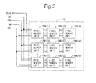
- FIG. 3 is a block diagram illustrating the configuration of the pixel memory portion 10.
- the pixel memory portion 10 includes nine pixel memory units PMU(1) to PMU(9), as shown in FIG. 3 . All of pixel memory units PMU(1) to PMU(9) are commonly provided with two-phase clock signals CK and CKB, white display voltage V W for setting the display state of the pixels to white display, and black display voltage V BL for setting the display state of the pixels to black display. Moreover, pixel memory unit PMU(1) is provided with display data DATA for specifying the display state of the pixel.
- each pixel memory unit PMU includes a flip-flop capable of holding one-bit data.
- flip-flops 11(1) to 11(9) respectively included in pixel memory units PMU(1) to PMU (9) are connected in series, as shown in FIG. 4 , forming a shift register 110. Accordingly, the display data DATA provided to pixel memory unit PMU(1) is transferred sequentially to pixel memory units PMU(2) to PMU(9) on the basis of the clock signals CK and CKB.
- the flip-flop within pixel memory unit PMU(3) in the first row, third column is connected to the flip-flop within pixel memory unit PMU(4) in the second row, third column, and the flip-flop within pixel memory unit PMU(6) in the second row, first column is connected to the flip-flop within pixel memory unit PMU(7) in the third row, first column, as shown in FIG. 3 .
- FIG. 1 is a block diagram illustrating the configuration of the pixel memory unit PMU.
- the pixel memory unit PMU includes a flip-flop 11, a voltage selection portion 12, and a liquid crystal capacitance 13, as shown in FIG. 1 .
- the flip-flop 11 receives signal Qn (an output signal of the flip-flop 11 in the previous stage) as an input signal, and outputs a "signal Qn+1" and a "logic-inversion signal of signal Qn+1" as output signals on the basis of clock signals CK and CKB. Note that the "logic-inversion signal of signal Qn+1" will be represented below as “signal Qn+1B".
- the voltage selection portion 12 selects either white display voltage VW or black display voltage VBL on the basis of a signal Qn+1 and a signal Qn+1B, and outputs the selected voltage as pixel electrode voltage VLC.
- the liquid crystal capacitance 13 is formed by the pixel electrode and the common electrode, and the display state of the pixel changes in accordance with the difference between pixel electrode voltage VLC and common electrode voltage VCOM.
- FIG. 5 is a circuit diagram illustrating a specific configuration example of the flip-flop 11.
- the flip-flop 11 is configured by a first latch portion 111 for taking in the signal Qn and holding it as transfer data, and a second latch portion 112 for taking in the transfer data and holding it as output data and outputting a signal Qn+1 and a signal Qn+1B on the basis of the output data.
- the first latch portion 111 is configured by a clocked inverter (referred to below as a "first clocked inverter") 141 in which signal Qn is provided to an input terminal, an inverter (referred to below as a “first inverter”) 142 connected at an input terminal to an output terminal of the first clocked inverter 141, and a clocked inverter (referred to below as a “second clocked inverter”) 143 connected at an input terminal to an output terminal of the first inverter 142 and connected at an output terminal to the input terminal of the first inverter 142.
- the output terminal of the first inverter 142 is also connected to an input terminal of a third clocked inverter 146 to be described later.
- the second latch portion 112 is configured by a clocked inverter (referred to below as the "third clocked inverter") 146 connected at an input terminal to the output terminal of the first inverter 142, an inverter (referred to below as a “second inverter”) 147 connected at an input terminal to an output terminal of the third clocked inverter 146, and a clocked inverter (referred to below as a "fourth clocked inverter”) 148 connected at an input terminal to an output terminal of the second inverter 147 and connected at an output terminal to the input terminal of the second inverter 147.
- signal Qn+1 is outputted from the output terminal of the second inverter 147
- signal Qn+1B is outputted from the output terminal of the fourth clocked inverter 148.
- first clocked inverter 141 and the fourth clocked inverter 148 function as inverters when the clock signal CK is at high level and the clock signal CKB is at low level, and their input and output terminals are electrically disconnected when the clock signal CK is at low level and the clock signal CKB is at high level.
- the second clocked inverter 143 and the third clocked inverter 146 have their input and output terminals electrically disconnected when the clock signal CK is at high level and the clock signal CKB is at low level, and they function as inverters when the clock signal CK is at low level and the clock signal CKB is at high level.
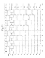
- the value of signal Qn which is provided during a period in which the clock signal CK is at high level and the clock signal CKB is at low level, is held in the first latch portion 111 as transfer data. Thereafter, at the timing when the clock signal CK changes from high level to low level and the clock signal CKB changes from low level to high level, the value of signal Qn being held in the first latch portion 111 as transfer data appears as the waveform of signal Qn+1. In addition, the transfer data is held in the second latch portion 112, so that the waveform of signal Qn+1 is maintained until the next time the clock signal CK changes from high level to low level and the clock signal CKB changes from low level to high level.
- FIG. 6 is a circuit diagram illustrating a specific configuration example of the voltage selection portion 12.
- the voltage selection portion 12 includes CMOS switches 121 and 122, each consisting of a P-type TFT and an N-type TFT.
- the CMOS switch 121 has an input terminal to which white display voltage VW is provided and an output terminal connected to the pixel electrode.
- Signal Qn+1 is provided to a gate terminal of the N-type TFT in the CMOS switch 121 and signal Qn+1B is provided to a gate terminal of the P-type TFT in the CMOS switch 121.
- the CMOS switch 122 has an input terminal to which black display voltage VBL is provided and an output terminal connected to the pixel electrode.
- Signal Qn+1B is provided to a gate terminal of the N-type TFT in the CMOS switch 122 and signal Qn+1 is provided to a gate terminal of the P-type TFT in the CMOS switch 122.
- the CMOS switch 121 is brought into ON state and the CMOS switch 122 is brought into OFF state, so that white display voltage VW is provided to the pixel electrode.
- the CMOS switch 121 is brought into OFF state and the CMOS switch 122 is brought into ON state, so that black display voltage VBL is provided to the pixel electrode.
- characters assigned to the first waveform in a signal waveform chart shown in FIG. 7 are intended in the present description to distinguish one-bit data inputted at each time to flip-flop 11(1) by display data DATA.
- “data D5" is inputted to flip-flop 11(1) by way of display data DATA during a period from time t5 to time t6.
- output signal Q1 of flip-flop 11 (1) is set to high level on the basis of the value of data D1. Note that output signal Q1 is provided to the voltage selection portion 12 (see FIG. 6 ) and is also provided to flip-flop 11(2).
- data D2 is inputted to flip-flop 11(1) as display data DATA. Since output signal Q1 of flip-flop 11 (1) is provided to flip-flop 11 (2), data D 1 is inputted to flip-flop 11(2) at this time. Moreover, at time t2, in the same manner at time t1, the clock signal CK changes from high level to low level, and the clock signal CKB changes from low level to high level. Accordingly, output signal Q1 of flip-flop 11(1) is maintained at high level on the basis of the value of data D2, and output signal Q2 of flip-flop 11(2) is set to high level on the basis of the value of data D1.
- the aforementioned output signals Q1 to Q9 and logic-inversion signals thereof are outputted. These signals are provided to the voltage selection portions 12 that correspond to their respective flip-flops 11.
- Common electrode voltage VCOM alternates between high level and low level every predetermined period of time.
- White display voltage VW and common electrode voltage VCOM are in the same phase.
- Black display voltage VBL and common electrode voltage VCOM are out of phase by 180 degrees.
- High-level potentials of white display voltage VW and black display voltage VBL are approximately equal to a high-level potential of common electrode voltage VCOM.
- FIG. 9 is a graph illustrating the relationship between voltage applied to liquid crystal and transmittance. Note that the relationship shown in FIG. 9 is about a liquid crystal display device employing a normally white mode. It can be appreciated from FIG. 9 that as the voltage applied to liquid crystal decreases, the transmittance increases, and as the voltage applied to liquid crystal increases, the transmittance decreases.
- voltage Va is equivalent to the difference between the potential of white display voltage VW and the potential of common electrode voltage VCOM
- voltage Vb is equivalent to the difference between the potential of black display voltage VBL and the potential of common electrode voltage VCOM.
- the display states of the pixels corresponding to pixel memory units PMU(1), PMU(4), PMU(5), PMU(7), PMU(8), and PMU(9) are set to white display
- the display states of the pixels corresponding to pixel memory units PMU(2), PMU(3), and PMU(6) are set to black display, as shown in FIG. 10 .
- output signals Q2, Q4, Q6, and Q8 of flip-flops 11(2), 11(4), 11(6), and 11(8) are set to high level
- output signals Q1, Q3, Q5, Q7 and Q9 of flip-flops 11(1), 11(3), 11(5), 11(7), and 11 (9) are set to low level.
- the display states of the pixels corresponding to pixel memory units PMU (2), PMU(4), PMU (6), and PMU(8) are set to white display
- the display states of the pixels corresponding to pixel memory units PMU(1), PMU(3), PMU(5), PMU(7), and PMU(9) are set to black display, as shown in FIG. 12 .
- each pixel memory unit PMU there are provided a voltage selection portion 12, which selects either white display voltage V W or black display voltage V BL in accordance with an output signal of the flip-flop 11 in the pixel memory unit PMU, and a liquid crystal capacitance 13, which reflects the voltage selected by the voltage selection portion 12 in the display state of the pixel that corresponds to the flip-flop 11.
- the flip-flops 11 respectively included in the pixel memory units PMU within the pixel memory portion 10 are connected in series, forming the shift register 110.
- the flip-flops 11 are capable of holding one-bit data, which makes it possible for each flip-flop 11 to transfer input data to the flip-flop 11 in the next stage and to set the display state of the corresponding pixel to a display state based on the input data.
- data corresponding to a display image can be provided to the flip-flops 11 within all of the pixel memory units PMU by providing display data DATA to the shift register 110, without providing a gate driver or a source driver.
- the contents of data latched in the flip-flops 11 are maintained until the next update, so that the same image can be continuously displayed without unnecessary power consumption.
- a liquid crystal display device capable of reducing a circuit area on a panel substrate compared to conventional devices and realizing low power consumption by drive using memory.
- the clock signals CK and CKB stop their action.
- the clock signals CK and CKB stop their action.
- FIG. 13 is a block diagram illustrating the configuration of a pixel memory portion 10 in a first variant of the embodiment.
- the flip-flop 11 within pixel memory unit PMU(13) in the first row, third column is connected to the flip-flop 11 within pixel memory unit PMU (14) in the second row, first column, and the flip-flop 11 within pixel memory unit PMU(16) in the second row, third column is connected to the flip-flop 11 within pixel memory unit PMU(17) in the third row, first column.
- display data DATA is transferred in the same direction in all of the rows.
- display data DATA can be readily generated.
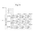
- FIG. 14 is a block diagram illustrating the configuration of a pixel memory portion 10 in a second variant of the embodiment.
- one shift register is constituted by the flip-flops 11 within all pixel memory units PMU in each row, rather than by the flip-flops 11 within all pixel memory units PMU included in the pixel memory portion 10.
- the pixel memory portion 10 includes three shift registers.
- a sampling circuit 15 for sampling display data DATA is provided in the pixel memory portion 10.
- the sampling circuit 15 provides display data DATA to pixel memory unit PMU(21) when data to be held in the flip-flops 11 within pixel memory units PMU (21) to PMU(23) is provided as the display data DATA, the sampling circuit 15 provides display data DATA to pixel memory unit PMU(24) when data to be held in the flip-flops 11 within pixel memory units PMU(24) to PMU(26) is provided as the display data DATA, and the sampling circuit 15 provides display data DATA to pixel memory unit PMU(27) when data to be held in the flip-flops 11 within pixel memory units PMU(27) to PMU(29) is provided as the display data DATA.
- data corresponding to a display image can be stored to the flip-flops 11 within all of the pixel memory units PMU included in the pixel memory portion 10.
- FIG. 15 is a block diagram illustrating the configuration of a pixel memory portion 10 in a third variant of the embodiment.
- one pixel is composed of two subpixels.
- a pixel memory unit provided so as to correspond to one subpixel is referred to as a "first pixel memory unit”
- a pixel memory unit provided so as to correspond to the other subpixel is referred to as a "second pixel memory unit”
- the pixel memory portion 10 includes nine first pixel memory units PMU1(1) to PMU1(9) and nine second pixel memory units PMU2(1) to PMU2(9), as shown in FIG. 15 .
- Clock signals CK and CKB, white display voltage VW, and black display voltage VBL are commonly provided to first pixel memory units PMU1(1) to PMU1(9) and second pixel memory units PMU2(1) to PMU2(9).
- display data different data is provided to first pixel memory unit PMU1(1) and second pixel memory unit PMU2(1).
- the display data provided to first pixel memory unit PMU1(1) is denoted by character DATA1
- the display data provided to second pixel memory unit PMU2(1) is denoted by character DATA2.
- first pixel memory units PMU1(1) to PMU1(9) constitute one shift register
- the flip-flops included in second pixel memory units PMU2(1) to PMU2(9) constitute another shift register. That is, in the present variant, two line shift registers are provided.
- one-bit data is held in each of the flip-flops within first pixel memory units PMU1(1) to PMU1(9) and each of the flip-flops within second pixel memory units PMU2 (1) to PMU2 (9), so that for each pixel, the display state of the subpixel that corresponds to the first pixel memory unit PMU1 (referred to below as a "first subpixel”) can be controlled independently of the display state of the subpixel that corresponds to the second pixel memory unit PMU2 (referred to below as a "second subpixel,”).
- first subpixel the display state of the subpixel that corresponds to the first pixel memory unit PMU1
- second subpixel the display state of the subpixel that corresponds to the second pixel memory unit PMU2
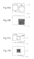
- a pixel electrode E1 which forms a first subpixel
- a pixel electrode E2 which forms a second subpixel
- a voltage based on data held in the flip-flop within the first pixel memory unit PMU1 is applied to the pixel electrode E1
- a voltage based on data held in the flip-flop within the second pixel memory unit PMU2 is applied to the pixel electrode E2.
- white display voltage VW is applied to the pixel electrode E1
- black display voltage VBL is applied to the pixel electrode E2
- the display states of the pixels are as shown in FIG. 16B .
- white display voltage VW can be applied to both of the pixel electrodes E1 and E2.
- black display voltage VBL can be applied to both of the pixel electrodes E1 and E2.
- black display voltage VBL it is also possible to apply black display voltage VBL to the pixel electrode E1 and white display voltage VW to the pixel electrode E2. In this manner, by setting the area of the pixel electrode E1 and the area of the pixel electrode E2 to differ from each other, it is rendered possible to achieve gradation display in four-levels of gradations.
- a pixel electrode E3, which forms a first subpixel, and a pixel electrode E4, which forms a second subpixel, can be formed on a panel substrate such that the pixel electrode E4 is enclosed by the pixel electrode E3 as shown in FIG. 17A .
- white display voltage VW is applied to the pixel electrode E3
- black display voltage VBL is applied to the pixel electrode E4
- the display states of the pixels are as shown in FIG. 17B .
- one pixel may be configured by three or more subpixels.
- the area ratio and the positional relationship can be variably set.
- one pixel may be configured by three subpixels, and R (red), G (green), and B (blue) data may be respectively provided to three line shift registers corresponding to the three subpixels. This enables color display.
- FIG. 18 is a circuit diagram illustrating a specific configuration example of the white display circuit 16.
- the white display circuit 16 includes two CMOS switches 161 and 162, each consisting of a P-type TFT and an N-type TFT, and an inverter 163.
- the CMOS switch 161 has an input terminal to which white display voltage VW is provided and an output terminal connected to the pixel electrode.
- An instruction signal S is provided to a gate terminal of the N-type TFT in the CMOS switch 161, and a gate terminal of the P-type TFT in the CMOS switch 161 is connected at to an output terminal of the inverter 163.
- the CMOS switch 162 has an input terminal to which signal Qn+1 is provided and an output terminal connected to the pixel electrode.
- a gate terminal of the N-type TFT in the CMOS switch 162 is connected to the output terminal of the inverter 163, and the instruction signal S is provided to a gate terminal of the P-type TFT in the CMOS switch 162.
- the inverter 163 has an input terminal to which the instruction signal S is provided and the output terminal connected to the gate terminal of the P-type TFT in the CMOS switch 161 and the gate terminal of the N-type TFT in the CMOS switch 162.
- the instruction signal is set at high level, and thereafter (after time t9 in FIGS. 7 and 11 ), the instruction signal is set at low level. Therefore, when an image is displayed or the contents of the image change, the image to be displayed is presented after full-screen white display is performed. As a result, noise can be barely perceived.
- the white display circuit 16 is provided for each pixel in the pixel memory portion 10.
- a voltage control circuit 17 is provided outside the pixel memory portion 10, as shown in FIG. 19 .
- White display voltage VWin, black display voltage VBLin, common electrode voltage VCOMin, and a control signal S are inputted into the voltage control circuit 17.
- the voltage control circuit 17 outputs white display voltage VW, black display voltage VBL, and common electrode voltage VCOM.
- FIG. 20 is a circuit diagram illustrating a specific configuration example of the voltage control circuit 17.
- the voltage control circuit 17 includes an inverter 171 and four CMOS switches 172 to 175, each consisting of a P-type TFT and an N-type TFT.
- the inverter 171 has an input terminal to which a control signal S is provided and an output terminal connected to a gate terminal of the N-type TFT in the CMOS switch 172, a gate terminal of the P-type TFT in the CMOS switch 173, a gate terminal of the N-type TFT in the CMOS switch 174, and a gate terminal of the P-type TFT in the CMOS switch 175.
- the CMOS switch 172 has an input terminal to which white display voltage VWin is provided and an output terminal connected to wiring for transmitting white display voltage VW.
- the gate terminal of the N-type TFT in the CMOS switch 172 is connected to the output terminal of the inverter 171, and the control signal S is provided to a gate terminal of the P-type TFT in the CMOS switch 172.
- the CMOS switch 173 has an input terminal to which common electrode voltage VCOMin is provided and an output terminal connected to wiring for transmitting white display voltage VW.
- the gate terminal of the P-type TFT in the CMOS switch 173 is connected to the output terminal of the inverter 171, and the control signal S is provided to a gate terminal of the N-type TFT in the CMOS switch 173.
- the CMOS switch 174 has an input terminal to which black display voltage VBLin is provided and an output terminal connected to wiring for transmitting black display voltage VBL.
- the gate terminal of the N-type TFT in the CMOS switch 174 is connected to the output terminal of the inverter 171, and the control signal S is provided to a gate terminal of the P-type TFT in the CMOS switch 174.
- the CMOS switch 175 has an input terminal to which common electrode voltage VCOMin is provided and an output terminal connected to wiring for transmitting black display voltage VBL.
- the gate terminal of the P-type TFT in the CMOS switch 175 is connected to the output terminal of the inverter 171, and the control signal S is provided to a gate terminal of the N-type TFT in the CMOS switch 175.
- the CMOS switches 172 and 174 are brought into ON state, and the CMOS switches 173 and 175 are brought into OFF state.
- white display voltage VWin is provided to the pixel memory portion 10 as white display voltage VW
- black display voltage VBLin is provided to the pixel memory portion 10 as black display voltage VBL.
- the display states of the pixels are based on data held in the flip-flops. Note that in a liquid crystal display device employing the normally black mode, when the control signal S is at high level, the display states of all pixels are set to black display.
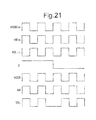
- the control signal S may be set at high level, and thereafter, the control signal S may be set at low level, as shown in FIG. 21 .
- the control signal S may be set at high level, and thereafter, the control signal S may be set at low level, as shown in FIG. 21 .
- FIG. 22 is a circuit diagram illustrating a specific configuration example of a flip-flop in a sixth variant of the embodiment.
- the flip-flop is configured by a first latch portion 113 for taking in signal Qn and holding it as transfer data, and a second latch portion 114 for taking in the transfer data and holding it as output data, and for outputting signals Qn+1 and Qn+1B on the basis of the output data.
- the first latch portion 113 includes a first clocked inverter 141 in which signal Qn is provided to an input terminal, and a capacitance 144 in which one end is connected to an output terminal of the first clocked inverter 141 and the other end is grounded. Note that the output terminal of the first clocked inverter 141 is also connected to an input terminal of a third clocked inverter 146 to be described later.
- the second latch portion 114 is configured by the third clocked inverter 146, which is connected at the input terminal to the output terminal of the first clocked inverter 141, a second inverter 147, which is connected at an input terminal to an output terminal of the third clocked inverter 146, and a fourth clocked inverter 148, which is connected at an input terminal to an output terminal of the second inverter 147 and is also connected at an output terminal to the input terminal of the second inverter 147.
- signal Qn+1 is outputted from the output terminal of the third clocked inverter 146
- signal Qn+1B is outputted from the output terminal of the second inverter 147.
- a charge is accumulated in the capacitance 144 in accordance with the value of signal Qn being provided during a period in which the clock signal CK is at high level and the clock signal CKB is at low level.
- the difference in potential between the ends of the capacitance 144 due to charge accumulation functions as transfer data.
- the value of signal Qn held in the first latch portion 113 as transfer data appears as the waveform of signal Qn+1.
- the transfer data is held in the second latch portion 114, the waveform of signal Qn+1 is maintained until the next time the clock signal CK changes from high level to low level and the clock signal CKB changes from low level to high level.
- the number of transistors included in the first latch portion 113 is six less than in the above-described embodiment.
- the present invention is not limited to this.
- the present invention can also be applied to other display devices such as organic EL (electroluminescence) display devices.
Landscapes
- Engineering & Computer Science (AREA)
- Physics & Mathematics (AREA)
- Computer Hardware Design (AREA)
- General Physics & Mathematics (AREA)
- Theoretical Computer Science (AREA)
- Chemical & Material Sciences (AREA)
- Crystallography & Structural Chemistry (AREA)
- Control Of Indicators Other Than Cathode Ray Tubes (AREA)
- Liquid Crystal Display Device Control (AREA)
- Liquid Crystal (AREA)
Applications Claiming Priority (2)
| Application Number | Priority Date | Filing Date | Title |
|---|---|---|---|
| JP2010125548 | 2010-06-01 | ||
| PCT/JP2011/058764 WO2011152120A1 (ja) | 2010-06-01 | 2011-04-07 | 表示装置 |
Publications (2)
| Publication Number | Publication Date |
|---|---|
| EP2579243A1 true EP2579243A1 (de) | 2013-04-10 |
| EP2579243A4 EP2579243A4 (de) | 2013-11-13 |
Family
ID=45066506
Family Applications (1)
| Application Number | Title | Priority Date | Filing Date |
|---|---|---|---|
| EP11789530.0A Withdrawn EP2579243A4 (de) | 2010-06-01 | 2011-04-07 | Anzeigevorrichtung |
Country Status (5)
| Country | Link |
|---|---|
| US (1) | US9368056B2 (de) |
| EP (1) | EP2579243A4 (de) |
| JP (1) | JP5631391B2 (de) |
| CN (1) | CN102804256B (de) |
| WO (1) | WO2011152120A1 (de) |
Cited By (1)
| Publication number | Priority date | Publication date | Assignee | Title |
|---|---|---|---|---|
| US11979688B2 (en) | 2020-08-21 | 2024-05-07 | Dualitas Ltd | Spatial light modulator |
Families Citing this family (16)
| Publication number | Priority date | Publication date | Assignee | Title |
|---|---|---|---|---|
| TW201430809A (zh) * | 2013-01-11 | 2014-08-01 | Sony Corp | 顯示面板、像素晶片及電子機器 |
| CA2873476A1 (en) * | 2014-12-08 | 2016-06-08 | Ignis Innovation Inc. | Smart-pixel display architecture |
| CN104485061B (zh) * | 2014-12-23 | 2018-03-23 | 上海天马有机发光显示技术有限公司 | 动态逻辑电路、栅极驱动电路、显示面板及显示装置 |
| CN104599622B (zh) * | 2015-02-13 | 2018-03-23 | 上海天马有机发光显示技术有限公司 | 动态逻辑电路、栅极驱动电路、显示面板及显示装置 |
| CN104933982B (zh) * | 2015-07-15 | 2017-06-30 | 京东方科技集团股份有限公司 | 移位寄存单元、移位寄存器、栅极驱动电路和显示装置 |
| JP2017083768A (ja) * | 2015-10-30 | 2017-05-18 | 株式会社ジャパンディスプレイ | 表示装置の駆動回路及び表示装置 |
| US10403984B2 (en) * | 2015-12-15 | 2019-09-03 | Kymeta Corporation | Distributed direct drive arrangement for driving cells |
| US10553167B2 (en) * | 2017-06-29 | 2020-02-04 | Japan Display Inc. | Display device |
| JP2019039949A (ja) * | 2017-08-22 | 2019-03-14 | 株式会社ジャパンディスプレイ | 表示装置 |
| JP6944334B2 (ja) * | 2017-10-16 | 2021-10-06 | 株式会社ジャパンディスプレイ | 表示装置 |
| JP6951237B2 (ja) * | 2017-12-25 | 2021-10-20 | 株式会社ジャパンディスプレイ | 表示装置 |
| US11049448B2 (en) | 2018-05-08 | 2021-06-29 | Apple Inc. | Memory-in-pixel architecture |
| US10867548B2 (en) * | 2018-05-08 | 2020-12-15 | Apple Inc. | Systems and methods for memory circuitry in an electronic display |
| US10909926B2 (en) | 2018-05-08 | 2021-02-02 | Apple Inc. | Pixel circuitry and operation for memory-containing electronic display |
| CN109272962B (zh) * | 2018-11-16 | 2021-04-27 | 京东方科技集团股份有限公司 | 像素内存储单元、像素内数据存储方法以及像素阵列 |
| JP2020154213A (ja) * | 2019-03-22 | 2020-09-24 | 株式会社ジャパンディスプレイ | 表示装置及び検出システム |
Family Cites Families (23)
| Publication number | Priority date | Publication date | Assignee | Title |
|---|---|---|---|---|
| US4464789A (en) * | 1980-05-19 | 1984-08-07 | Environmental Research Institute Of Michigan | Image analyzer for processing multiple frames of image data |
| US4996523A (en) | 1988-10-20 | 1991-02-26 | Eastman Kodak Company | Electroluminescent storage display with improved intensity driver circuits |
| US5945972A (en) | 1995-11-30 | 1999-08-31 | Kabushiki Kaisha Toshiba | Display device |
| JP3488577B2 (ja) * | 1996-08-30 | 2004-01-19 | 株式会社東芝 | マトリクス型表示装置 |
| US6067065A (en) * | 1998-05-08 | 2000-05-23 | Aurora Systems, Inc. | Method for modulating a multiplexed pixel display |
| JP3589926B2 (ja) * | 2000-02-02 | 2004-11-17 | シャープ株式会社 | シフトレジスタ回路および画像表示装置 |
| US6980184B1 (en) * | 2000-09-27 | 2005-12-27 | Alien Technology Corporation | Display devices and integrated circuits |
| JP3540772B2 (ja) * | 2001-05-23 | 2004-07-07 | 三洋電機株式会社 | 表示装置およびその制御方法 |
| US6940482B2 (en) | 2001-07-13 | 2005-09-06 | Seiko Epson Corporation | Electrooptic device and electronic apparatus |
| JP4158441B2 (ja) * | 2001-07-13 | 2008-10-01 | セイコーエプソン株式会社 | 電気光学装置および電子機器 |
| TWI248056B (en) | 2001-10-19 | 2006-01-21 | Sony Corp | Level converter circuits, display device and portable terminal device |
| JP2004177433A (ja) * | 2002-11-22 | 2004-06-24 | Sharp Corp | シフトレジスタブロック、それを備えたデータ信号線駆動回路及び表示装置 |
| JP3821111B2 (ja) * | 2003-05-12 | 2006-09-13 | セイコーエプソン株式会社 | データドライバ及び電気光学装置 |
| JP4576836B2 (ja) * | 2003-12-24 | 2010-11-10 | セイコーエプソン株式会社 | 画素回路、電気光学装置および電子機器 |
| US9922600B2 (en) * | 2005-12-02 | 2018-03-20 | Semiconductor Energy Laboratory Co., Ltd. | Display device |
| JP2007199441A (ja) * | 2006-01-27 | 2007-08-09 | Hitachi Displays Ltd | 画像表示装置 |
| JP2007240969A (ja) * | 2006-03-09 | 2007-09-20 | Epson Imaging Devices Corp | 電気光学装置および電子機器 |
| JP2007286237A (ja) | 2006-04-14 | 2007-11-01 | Sharp Corp | 表示装置 |
| WO2008044666A1 (en) * | 2006-10-13 | 2008-04-17 | Semiconductor Energy Laboratory Co., Ltd. | Source line driver circuit and driving method |
| JP2008241832A (ja) * | 2007-03-26 | 2008-10-09 | Seiko Epson Corp | 液晶装置、画素回路、アクティブマトリクス基板、および電子機器 |
| JP2009229850A (ja) * | 2008-03-24 | 2009-10-08 | Seiko Epson Corp | 画素回路、電気泳動表示装置及びその駆動方法、並びに電子機器 |
| US8497821B2 (en) * | 2009-02-16 | 2013-07-30 | Global Oled Technology Llc | Chiplet display device with serial control |
| US8803857B2 (en) * | 2011-02-10 | 2014-08-12 | Ronald S. Cok | Chiplet display device with serial control |
-
2011
- 2011-04-07 JP JP2012518281A patent/JP5631391B2/ja not_active Expired - Fee Related
- 2011-04-07 CN CN201180013959.3A patent/CN102804256B/zh not_active Expired - Fee Related
- 2011-04-07 US US13/583,086 patent/US9368056B2/en active Active
- 2011-04-07 WO PCT/JP2011/058764 patent/WO2011152120A1/ja not_active Ceased
- 2011-04-07 EP EP11789530.0A patent/EP2579243A4/de not_active Withdrawn
Cited By (1)
| Publication number | Priority date | Publication date | Assignee | Title |
|---|---|---|---|---|
| US11979688B2 (en) | 2020-08-21 | 2024-05-07 | Dualitas Ltd | Spatial light modulator |
Also Published As
| Publication number | Publication date |
|---|---|
| CN102804256B (zh) | 2015-02-25 |
| US9368056B2 (en) | 2016-06-14 |
| US20130002626A1 (en) | 2013-01-03 |
| JP5631391B2 (ja) | 2014-11-26 |
| CN102804256A (zh) | 2012-11-28 |
| EP2579243A4 (de) | 2013-11-13 |
| JPWO2011152120A1 (ja) | 2013-07-25 |
| WO2011152120A1 (ja) | 2011-12-08 |
Similar Documents
| Publication | Publication Date | Title |
|---|---|---|
| US9368056B2 (en) | Display device | |
| US9299302B2 (en) | Display device | |
| US11151946B2 (en) | Shift register unit and driving method, gate driving circuit, and display device | |
| US11837147B2 (en) | Display substrate, display panel, display apparatus and display driving method | |
| EP3933819A1 (de) | Anzeigetafel, anzeigevorrichtung und ansteuerverfahren | |
| US9548026B2 (en) | Emission control driver and organic light emitting display device having the same | |
| US20210358365A1 (en) | Shift Register Unit and Driving Method Thereof, Gate Driving Circuit, and Display Device | |
| US8988406B2 (en) | Scan driver and organic light emitting display using the scan driver | |
| US20180151145A1 (en) | Display device subpixel activation patterns | |
| EP2610852B1 (de) | Flüssigkristallanzeigevorrichtung, Antriebsvorrichtung für Flüssigkristallanzeigetafel und Flüssigkristallanzeigetafel | |
| US20220028340A9 (en) | Shift register unit, gate driving circuit, display device and driving method | |
| JP2006018299A (ja) | ゲートドライバが内蔵された液晶パネル及びその駆動方法 | |
| CN106875917B (zh) | 扫描驱动电路与阵列基板 | |
| WO2013168603A1 (ja) | 走査信号線駆動回路およびそれを備える表示装置 | |
| US9041693B2 (en) | Scan driver and organic light emitting display using the scan driver | |
| KR20060126231A (ko) | 공유 회로를 이용하는 평판 표시 장치의 게이트 라인 구동장치 및 방법 | |
| US10998069B2 (en) | Shift register and electronic device having the same | |
| US20250209990A1 (en) | Scan Signal Generation Circuit and Display Device Including the Same | |
| CN107452349B (zh) | 一种驱动电路及液晶显示装置 | |
| KR102854036B1 (ko) | 스캔 구동부 및 이를 포함하는 표시장치 | |
| KR101609378B1 (ko) | 액정표시장치 및 그 구동방법 | |
| US20240347017A1 (en) | Display apparatus, driving method, and electronic device | |
| CN117275398B (zh) | 一种显示面板及其驱动方法、显示装置 | |
| KR20240094481A (ko) | 게이트 드라이버를 갖는 디스플레이 장치 | |
| JP2012128095A (ja) | ソースドライバおよび液晶表示装置 |
Legal Events
| Date | Code | Title | Description |
|---|---|---|---|
| PUAI | Public reference made under article 153(3) epc to a published international application that has entered the european phase |
Free format text: ORIGINAL CODE: 0009012 |
|
| 17P | Request for examination filed |
Effective date: 20120824 |
|
| AK | Designated contracting states |
Kind code of ref document: A1 Designated state(s): AL AT BE BG CH CY CZ DE DK EE ES FI FR GB GR HR HU IE IS IT LI LT LU LV MC MK MT NL NO PL PT RO RS SE SI SK SM TR |
|
| DAX | Request for extension of the european patent (deleted) | ||
| A4 | Supplementary search report drawn up and despatched |
Effective date: 20131016 |
|
| RIC1 | Information provided on ipc code assigned before grant |
Ipc: G09G 3/36 20060101AFI20131007BHEP Ipc: G09G 3/20 20060101ALI20131007BHEP Ipc: G02F 1/133 20060101ALI20131007BHEP |
|
| STAA | Information on the status of an ep patent application or granted ep patent |
Free format text: STATUS: THE APPLICATION HAS BEEN WITHDRAWN |
|
| 18W | Application withdrawn |
Effective date: 20150227 |