EP2562825A2 - Abziehstruktur für Substrat einer photoelektrischen Vorrichtung und Verfahren dafür - Google Patents
Abziehstruktur für Substrat einer photoelektrischen Vorrichtung und Verfahren dafür Download PDFInfo
- Publication number
- EP2562825A2 EP2562825A2 EP11401601A EP11401601A EP2562825A2 EP 2562825 A2 EP2562825 A2 EP 2562825A2 EP 11401601 A EP11401601 A EP 11401601A EP 11401601 A EP11401601 A EP 11401601A EP 2562825 A2 EP2562825 A2 EP 2562825A2
- Authority
- EP
- European Patent Office
- Prior art keywords
- substrate
- layer
- lift
- etch
- pattern
- Prior art date
- Legal status (The legal status is an assumption and is not a legal conclusion. Google has not performed a legal analysis and makes no representation as to the accuracy of the status listed.)
- Granted
Links
Images


Classifications
-
- H—ELECTRICITY
- H10—SEMICONDUCTOR DEVICES; ELECTRIC SOLID-STATE DEVICES NOT OTHERWISE PROVIDED FOR
- H10F—INORGANIC SEMICONDUCTOR DEVICES SENSITIVE TO INFRARED RADIATION, LIGHT, ELECTROMAGNETIC RADIATION OF SHORTER WAVELENGTH OR CORPUSCULAR RADIATION
- H10F10/00—Individual photovoltaic cells, e.g. solar cells
- H10F10/10—Individual photovoltaic cells, e.g. solar cells having potential barriers
- H10F10/14—Photovoltaic cells having only PN homojunction potential barriers
- H10F10/142—Photovoltaic cells having only PN homojunction potential barriers comprising multiple PN homojunctions, e.g. tandem cells
- H10F10/1425—Inverted metamorphic multi-junction [IMM] photovoltaic cells
-
- H—ELECTRICITY
- H10—SEMICONDUCTOR DEVICES; ELECTRIC SOLID-STATE DEVICES NOT OTHERWISE PROVIDED FOR
- H10F—INORGANIC SEMICONDUCTOR DEVICES SENSITIVE TO INFRARED RADIATION, LIGHT, ELECTROMAGNETIC RADIATION OF SHORTER WAVELENGTH OR CORPUSCULAR RADIATION
- H10F10/00—Individual photovoltaic cells, e.g. solar cells
- H10F10/10—Individual photovoltaic cells, e.g. solar cells having potential barriers
- H10F10/14—Photovoltaic cells having only PN homojunction potential barriers
- H10F10/144—Photovoltaic cells having only PN homojunction potential barriers comprising only Group III-V materials, e.g. GaAs,AlGaAs, or InP photovoltaic cells
-
- H—ELECTRICITY
- H10—SEMICONDUCTOR DEVICES; ELECTRIC SOLID-STATE DEVICES NOT OTHERWISE PROVIDED FOR
- H10F—INORGANIC SEMICONDUCTOR DEVICES SENSITIVE TO INFRARED RADIATION, LIGHT, ELECTROMAGNETIC RADIATION OF SHORTER WAVELENGTH OR CORPUSCULAR RADIATION
- H10F71/00—Manufacture or treatment of devices covered by this subclass
- H10F71/127—The active layers comprising only Group III-V materials, e.g. GaAs or InP
-
- H—ELECTRICITY
- H10—SEMICONDUCTOR DEVICES; ELECTRIC SOLID-STATE DEVICES NOT OTHERWISE PROVIDED FOR
- H10F—INORGANIC SEMICONDUCTOR DEVICES SENSITIVE TO INFRARED RADIATION, LIGHT, ELECTROMAGNETIC RADIATION OF SHORTER WAVELENGTH OR CORPUSCULAR RADIATION
- H10F71/00—Manufacture or treatment of devices covered by this subclass
- H10F71/139—Manufacture or treatment of devices covered by this subclass using temporary substrates
-
- H—ELECTRICITY
- H10—SEMICONDUCTOR DEVICES; ELECTRIC SOLID-STATE DEVICES NOT OTHERWISE PROVIDED FOR
- H10F—INORGANIC SEMICONDUCTOR DEVICES SENSITIVE TO INFRARED RADIATION, LIGHT, ELECTROMAGNETIC RADIATION OF SHORTER WAVELENGTH OR CORPUSCULAR RADIATION
- H10F77/00—Constructional details of devices covered by this subclass
- H10F77/20—Electrodes
- H10F77/206—Electrodes for devices having potential barriers
- H10F77/211—Electrodes for devices having potential barriers for photovoltaic cells
- H10F77/219—Arrangements for electrodes of back-contact photovoltaic cells
-
- Y—GENERAL TAGGING OF NEW TECHNOLOGICAL DEVELOPMENTS; GENERAL TAGGING OF CROSS-SECTIONAL TECHNOLOGIES SPANNING OVER SEVERAL SECTIONS OF THE IPC; TECHNICAL SUBJECTS COVERED BY FORMER USPC CROSS-REFERENCE ART COLLECTIONS [XRACs] AND DIGESTS
- Y02—TECHNOLOGIES OR APPLICATIONS FOR MITIGATION OR ADAPTATION AGAINST CLIMATE CHANGE
- Y02E—REDUCTION OF GREENHOUSE GAS [GHG] EMISSIONS, RELATED TO ENERGY GENERATION, TRANSMISSION OR DISTRIBUTION
- Y02E10/00—Energy generation through renewable energy sources
- Y02E10/50—Photovoltaic [PV] energy
- Y02E10/544—Solar cells from Group III-V materials
Definitions
- the present invention relates to a lift-off structure for substrate of a photoelectric device and the method thereof, and more particularly, to a lift-off process adapted for semiconductor and photoelectric industries.
- III-V multi-junction solar cell can absorb solar energy in a wider wavelength range and as a result its photoelectric conversion efficiency, that is able 42% in laboratory test, is higher than the usual flat-plate solar cell.
- the III-V multi-junction solar cells are especially suitable to be applied in large ground-mounted solar power systems for providing electricity in residential sector.
- the electricity output of a solar cell is influenced by the intensity of the light that shines on it while the electricity output of the solar cell can be fed to and used by an external device through its metal electrodes.
- an electric current of several amperes or more flowing through the components inside the solar cell there will be an electric current of several amperes or more flowing through the components inside the solar cell, and consequently, if there is any components inside the solar cell that is designed with poor heat dissipating ability in view of thermal resistance, the temperature of such component as well as the whole solar cell will raise after light shines on the solar cell, causing the conversion efficiency of the solar cell to deteriorate, i.e. the current-voltage characteristics of the solar cell are adversely affected.
- the solar cell that is formed on a raw GaAs substrate is first being attached to an adhesive layer of a metal substrate that is formed with high heat-dissipating ability by wafer bonding, and then a chemical solution, such as a mixing solution of ammonia, hydrogen peroxide and water, is used for etching the raw GaAs substrate so as to prepare the same for having a layer of metallic electrode grids to be formed therein, as shown in FIG. 1 .
- a chemical solution such as a mixing solution of ammonia, hydrogen peroxide and water
- the raw GaAs substrate will be etching away by the chemical solution in the aforesaid conventional solar cell manufacturing process, thus such manufacturing process is disadvantageous in that: first, the raw substrate can not be recycled and used repetitively; and second, the manufacturing cost is increased comparing with those solar cells without the metal substrate with high heat-dissipating ability, owing to the acquisition costs of the raw substrate and the metal substrate with high heat-dissipating ability, and the waste management cost for treating the arsenic-containing waste liquid resulting from the manufacturing process.
- a prior-art technique in which the raw substrate is separated from the solar cell and thus removed by the selectively etching of a sacrificial layer using a chemical solution.
- the method for lifting off substrates of such photoelectric devices is performed through the use of a thin layer of high-aluminum-containing AlGaAs sacrificial film that is sandwiched between the corresponding epitaxial substrate and photoelectric film, as the high-aluminum-containing AlGaAs sacrificial layer is featured by that it is easy to reacted to and thus be etched by hydrofluoric acid-containing solution.
- the lateral etching rate of the sacrificial layer can be very low due to the restriction of capillary action and the limitation relating to a minimum contact area. Therefore, it can take a very long period of time just for performing a substrate lift-off process upon a large-size wafer. Thus, such prior-art technique for separating the raw substrate might not be feasible for industrial mass production.
- the object of the present invention is to provide a lift-off structure for substrate of a photoelectric device and the method thereof, by that not only contact area for etching can be increased effectively, but also the time spent for substrate lifting-off can be reduced significantly.
- the present invention provides a lift-off structure, adapted for a substrate composed of a buffer layer, an etch stop layer, a protective layer, a sacrificial layer, and a photoelectric element in a manner that the buffer layer is formed on one side of the substrate, the etch stop layer is formed on a side of the buffer layer that is opposite to the substrate, the protective layer is formed on a side of the etch stop layer that is opposite to the buffer layer, the sacrificial layer is formed on a side of the protective layer that is opposite to the etch stop layer, and the photoelectric element is formed on a side of the sacrificial layer that is opposite to the protective layer, the lift-off structure comprising: a metal layer, formed on a side of the photoelectric element that is opposite to the sacrificial layer while allowing the metal layer to be formed with at least one pattern in a manner that each pattern is formed with at least one internal etch channel while allowing any two neighboring patterns to be separated by one external etch channel.
- a lithography/deposition method for forming patterns on the metal layer which comprises the steps of:
- the time spent for substrate lifting-off can be reduced significantly since the etching solution can be enabled to flow through the external etch channels and the internal etch channels so as to speed up the desired side etching effect.
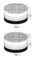
- FIG. 1 is a schematic diagram showing a lift-off structure for substrate of a photoelectric device according to a first embodiment of the invention.
- FIG. 2 is a schematic diagram showing a lift-off structure for substrate of a photoelectric device according to a second embodiment of the invention.
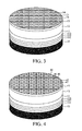
- FIG. 3 is a schematic diagram showing a lift-off structure for substrate of a photoelectric device according to a third embodiment of the invention.
- FIG. 4 is a schematic diagram showing a lift-off structure for substrate of a photoelectric device according to a fourth embodiment of the invention.
- FIG. 5 is a schematic diagram showing a lift-off structure for substrate of a photoelectric device according to a fifth embodiment of the invention.
- FIG. 6 is a schematic diagram showing a lift-off structure for substrate of a photoelectric device according to a sixth embodiment of the invention.
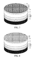
- FIG. 7 is a schematic diagram showing a lift-off structure for substrate of a photoelectric device according to a seventh embodiment of the invention.
- FIG. 8 is a schematic diagram showing a lift-off structure for substrate of a photoelectric device according to an eighth embodiment of the invention.
- FIG. 9 is a schematic diagram showing a lift-off structure for substrate of a photoelectric device according to a ninth embodiment of the invention.
- FIG. 10 is a schematic diagram showing how an etching solution is designed to flow during the lifting off of a substrate according to the present invention.
- FIG. 11 is a schematic diagram showing a substrate after being lift off according to the present invention.
- FIG. 1 is a schematic diagram showing a lift-off structure for substrate of a photoelectric device according to a first embodiment of the invention.
- the present invention provides a lift-off structure, which is adapted for a substrate 10 composed of a buffer layer 101, an etch stop layer 102, a protective layer 103, a sacrificial layer 11, and a photoelectric element 12 in a manner that the buffer layer 101 is formed on one side of the substrate 10, the etch stop layer 102 is formed on a side of the buffer layer 101 that is opposite to the substrate, the protective layer 103 is formed on a side of the etch stop layer 102 that is opposite to the buffer layer 101, the sacrificial layer 11 is formed on a side of the protective layer 103 that is opposite to the etch stop layer 102, and the photoelectric element 12 is formed on a side of the sacrificial layer 11 that is opposite to the protective layer 103.
- the lift-off structure comprises: a metal layer 13, which is formed on a side of the photoelectric element 12 that is opposite to the sacrificial layer 11 while allowing the metal layer 13 to be formed with at least one pattern in a manner that each pattern is formed with an internal etch channel 15 while allowing any two neighboring patterns to be separated by one external etch channel 14.
- each pattern can be formed in a shape of a polygon and also each internal etch channel 15 can be formed in a shape of a polygon, and in this embodiment, the pattern is formed as a rectangle and the internal etch channel is formed as a long stripe at a side of the rectangle-shaped pattern.
- the description relating to the embodiments that is provided hereinafter is focused on the configuration of the metal layer.
- the metal layer is disposed on the substrate at a position that same as that in the aforesaid embodiment, and also as the substrate is structured the same as the one shown in the aforesaid embodiment, the structure of the substrates used in the following embodiments will not be described further and using the same numbering.
- FIG. 2 is a schematic diagram showing a lift-off structure for substrate of a photoelectric device according to a second embodiment of the invention.
- the metal layer 23 is formed on a side of the photoelectric element 12 that is opposite to the sacrificial layer 11 while allowing the metal layer 23 to be formed with at least one pattern in a manner that each pattern, being formed in a shape of a rectangular, is configured with one first internal etch channel 25 and one second internal etch channel 26 respectively at sides of the corresponding rectangular-shaped pattern that are opposite to each other, while allowing any two neighboring patterns to be separated by one external etch channel 24.
- each of the first and the second internal etch channels 25, 26 can be formed in a shape of a polygon, and in this embodiment, each of the first and the second internal etch channels 25, 26 is formed as a long stripe.
- FIG. 3 is a schematic diagram showing a lift-off structure for substrate of a photoelectric device according to a third embodiment of the invention.
- the metal layer 33 is formed on a side of the photoelectric element 12 that is opposite to the sacrificial layer 11 while allowing the metal layer 33 to be formed with at least one pattern in a manner that each pattern, being formed in a shape of a rectangular, is configured with one first internal etch channel 35 and one second internal etch channel 36 at the same side of the corresponding rectangular-shaped pattern, while allowing any two neighboring patterns to be separated by one external etch channel 34.
- each of the first and the second internal etch channels 35, 36 can be formed in a shape of a polygon, and in this embodiment, each of the first and the second internal etch channels 35, 36 is formed as a long stripe.
- FIG. 4 is a schematic diagram showing a lift-off structure for substrate of a photoelectric device according to a fourth embodiment of the invention.
- the metal layer 43 is formed on a side of the photoelectric element 12 that is opposite to the sacrificial layer 11 while allowing the metal layer 43 to be formed with at least one pattern in a manner that each pattern, being formed in a shape of a rectangular, is configured with one first internal etch channel 45, one second internal etch channel 46, one third internal etch channel 47 and one fourth internal etch channel 48 respectively at the four sides of the corresponding rectangular-shaped pattern, while allowing any two neighboring patterns to be separated by one external etch channel 44.
- each of the first, the second, the third and the fourth internal etch channels 45, 46, 47 and 48 can be formed in a shape of a polygon, and in this embodiment, each of the first, the second, the third and the fourth internal etch channels 45, 46, 47 and 48 is formed as a long stripe.
- FIG. 5 is a schematic diagram showing a lift-off structure for substrate of a photoelectric device according to a fifth embodiment of the invention.
- the metal layer 53 is formed on a side of the photoelectric element 12 that is opposite to the sacrificial layer 11 while allowing the metal layer 53 to be formed with at least one pattern in a manner that each pattern, being formed in a shape of a rectangular, is configured with one internal etch channel 55 at a corner of the corresponding rectangular-shaped pattern, while allowing any two neighboring patterns to be separated by one external etch channel 54.
- the internal etch channel 55 can be formed in a shape of a polygon, and in this embodiment, the internal etch channel 55 is formed as a long stripe.
- FIG. 6 is a schematic diagram showing a lift-off structure for substrate of a photoelectric device according to a sixth embodiment of the invention.
- the metal layer 63 is formed on a side of the photoelectric element 12 that is opposite to the sacrificial layer 11 while allowing the metal layer 63 to be formed with at least one pattern in a manner that each pattern, being formed in a shape of a rectangular, is configured with one first internal etch channel 65 and one second internal etch channel 66 respectively at two different corners of the corresponding rectangular-shaped pattern, while allowing any two neighboring patterns to be separated by one external etch channel 64.
- the first and the second internal etch channels 65, 66 can be formed in a shape of a polygon, and in this embodiment, the first and the second internal etch channels 65, 66 are formed as a long stripe.
- FIG. 7 is a schematic diagram showing a lift-off structure for substrate of a photoelectric device according to a seventh embodiment of the invention.
- the metal layer 73 is formed on a side of the photoelectric element 12 that is opposite to the sacrificial layer 11 while allowing the metal layer 73 to be formed with at least one pattern in a manner that each pattern, being formed in a shape of a rectangular, is configured with one first internal etch channel 75, one second internal etch channel 76, one third internal etch channel 77 and one fourth internal etch channel 78 respectively at the four corners of the corresponding rectangular-shaped pattern, while allowing any two neighboring patterns to be separated by one external etch channel 74.
- first, the second, the third and the fourth internal etch channels 75, 76, 77 and 78 can be formed in a shape of a polygon, and in this embodiment, the first, the second, the third and the fourth internal etch channels 75, 76, 77 and 78 are formed as a long stripe.
- FIG. 8 is a schematic diagram showing a lift-off structure for substrate of a photoelectric device according to an eighth embodiment of the invention.
- the metal layer 83 is formed on a side of the photoelectric element 12 that is opposite to the sacrificial layer 11 while allowing the metal layer 83 to be formed with at least one pattern in a manner that each pattern, being formed in a shape of a rectangular, is configured with one triangle-shaped internal etch channel 85 at a side of the corresponding rectangular-shaped pattern, while allowing any two neighboring patterns to be separated by one external etch channel 84.
- the internal etch channel 85 can be formed in a shape of a polygon, and in this embodiment, the internal etch channel 85 is formed as a triangle.
- FIG. 9 is a schematic diagram showing a lift-off structure for substrate of a photoelectric device according to a ninth embodiment of the invention.
- the metal layer 93 is formed on a side of the photoelectric element 12 that is opposite to the sacrificial layer 11 while allowing the metal layer 93 to be formed with at least one pattern in a manner that each pattern, being formed in a shape of a rectangular, is configured with one triangle-shaped internal etch channel 95 at a corner of the corresponding rectangular-shaped pattern, while allowing any two neighboring patterns to be separated by one external etch channel 94.
- the internal etch channel 95 can be formed in a shape of a polygon, and in this embodiment, the internal etch channel 95 is formed as a triangle.
- FIG. 10 and FIG. 11 are schematic diagrams respectively showing how an etching solution is designed to flow during the lifting off of a substrate, and a substrate after being lift-off according to the present invention.
- any two neighboring patterns are separated by an external etch channel and each pattern itself is designed to have at least one internal etch channel defined therein while allowing the internal etch channels to be arranged in fluid communication with the external etch channels.
- the etch solution is able to etch and form the plural internal etch channels and the external etch channels respectively to a depth reaching the sacrificial layer, in the directions indicating by the arrows shown in FIG. 10 all the way toward the sacrificial layer 11.
- the etching solution will start to etch the sacrificial layer 11 until the sacrificial layer 11 is being etched away completely for completing the lifting off of the substrate 10, resulting that the time required for completing the etching of the sacrificial layer is reduced and thus the time spent for substrate lifting-off can be reduced significantly.
- the time spent for substrate lifting-off can be reduced significantly since the etching solution can be enabled to flow through the external etch channels and the internal etch channels so as to speed up the desired side etching effect.
Landscapes
- Weting (AREA)
- Photovoltaic Devices (AREA)
Applications Claiming Priority (1)
| Application Number | Priority Date | Filing Date | Title |
|---|---|---|---|
| TW100130742A TWI585990B (zh) | 2011-08-26 | 2011-08-26 | 用於光電元件之基板的剝離結構 |
Publications (3)
| Publication Number | Publication Date |
|---|---|
| EP2562825A2 true EP2562825A2 (de) | 2013-02-27 |
| EP2562825A3 EP2562825A3 (de) | 2013-09-25 |
| EP2562825B1 EP2562825B1 (de) | 2019-01-16 |
Family
ID=44883144
Family Applications (1)
| Application Number | Title | Priority Date | Filing Date |
|---|---|---|---|
| EP11401601.7A Not-in-force EP2562825B1 (de) | 2011-08-26 | 2011-09-27 | Abziehstruktur für Substrat einer photoelektrischen Vorrichtung und Verfahren dafür |
Country Status (3)
| Country | Link |
|---|---|
| US (1) | US8497421B2 (de) |
| EP (1) | EP2562825B1 (de) |
| TW (1) | TWI585990B (de) |
Cited By (1)
| Publication number | Priority date | Publication date | Assignee | Title |
|---|---|---|---|---|
| US11268681B2 (en) | 2018-12-31 | 2022-03-08 | Zedel S.A.S. | Load balancing device for improving the holding of a headlamp on the head of a user |
Families Citing this family (1)
| Publication number | Priority date | Publication date | Assignee | Title |
|---|---|---|---|---|
| CN119230379A (zh) * | 2023-06-29 | 2024-12-31 | 苏州能讯高能半导体有限公司 | 外延结构及其制备方法 |
Family Cites Families (11)
| Publication number | Priority date | Publication date | Assignee | Title |
|---|---|---|---|---|
| US5626687A (en) * | 1995-03-29 | 1997-05-06 | The United States Of America As Represented By The United States Department Of Energy | Thermophotovoltaic in-situ mirror cell |
| NL1010635C2 (nl) * | 1998-11-23 | 2000-05-24 | Stichting Energie | Werkwijze voor het vervaardigen van een metallisatiepatroon op een fotovoltaïsche cel. |
| US7427526B2 (en) * | 1999-12-20 | 2008-09-23 | The Penn State Research Foundation | Deposited thin films and their use in separation and sacrificial layer applications |
| US8173891B2 (en) * | 2002-05-21 | 2012-05-08 | Alliance For Sustainable Energy, Llc | Monolithic, multi-bandgap, tandem, ultra-thin, strain-counterbalanced, photovoltaic energy converters with optimal subcell bandgaps |
| JP4097510B2 (ja) * | 2002-11-20 | 2008-06-11 | 株式会社沖データ | 半導体装置の製造方法 |
| JP4136795B2 (ja) * | 2003-06-03 | 2008-08-20 | 株式会社沖データ | 半導体装置の製造方法 |
| JP4315744B2 (ja) * | 2003-06-25 | 2009-08-19 | 株式会社沖データ | 積層体及び半導体装置の製造方法 |
| JP4518886B2 (ja) * | 2004-09-09 | 2010-08-04 | シャープ株式会社 | 半導体素子の製造方法 |
| JP2008053250A (ja) * | 2006-08-22 | 2008-03-06 | Sony Corp | 半導体装置の製造方法 |
| CN101785115B (zh) * | 2007-07-03 | 2013-05-08 | 微连器件公司 | 薄膜ⅲ-ⅴ族化合物太阳能电池 |
| EP2521189A3 (de) * | 2011-04-29 | 2013-05-01 | Institute of Nuclear Energy Research Atomic Energy Council | Lift-off-Struktur für ein Substrat eines photoelektrischen Gerätes und deren Verfahren |
-
2011
- 2011-08-26 TW TW100130742A patent/TWI585990B/zh not_active IP Right Cessation
- 2011-09-20 US US13/236,859 patent/US8497421B2/en not_active Expired - Fee Related
- 2011-09-27 EP EP11401601.7A patent/EP2562825B1/de not_active Not-in-force
Non-Patent Citations (1)
| Title |
|---|
| None |
Cited By (1)
| Publication number | Priority date | Publication date | Assignee | Title |
|---|---|---|---|---|
| US11268681B2 (en) | 2018-12-31 | 2022-03-08 | Zedel S.A.S. | Load balancing device for improving the holding of a headlamp on the head of a user |
Also Published As
| Publication number | Publication date |
|---|---|
| US8497421B2 (en) | 2013-07-30 |
| EP2562825A3 (de) | 2013-09-25 |
| TWI585990B (zh) | 2017-06-01 |
| TW201310670A (zh) | 2013-03-01 |
| US20130048058A1 (en) | 2013-02-28 |
| EP2562825B1 (de) | 2019-01-16 |
Similar Documents
| Publication | Publication Date | Title |
|---|---|---|
| JP6422426B2 (ja) | 太陽電池 | |
| CN105518871B (zh) | 增强的多孔化 | |
| JP4944240B1 (ja) | 裏面電極型太陽電池セル、配線シート付き裏面電極型太陽電池セル、太陽電池モジュール、配線シート付き裏面電極型太陽電池セルの製造方法および太陽電池モジュールの製造方法 | |
| US8575004B2 (en) | Lift-off structure for substrate of a photoelectric device and the method thereof | |
| WO2016095859A1 (zh) | 太阳能电池片、太阳能电池组件和旁路二极管的组装方法 | |
| JP5099698B2 (ja) | 裏面電極型太陽電池および太陽電池モジュール | |
| CN102779894A (zh) | 太阳能电池的电极的制造方法与装置 | |
| US8497421B2 (en) | Lift-off structure for substrate of a photoelectric device and method thereof | |
| EP2521189A2 (de) | Lift-off-Struktur für ein Substrat eines photoelektrischen Gerätes und deren Verfahren | |
| CN105552145B (zh) | 一种晶硅太阳能电池 | |
| CN204991723U (zh) | 一种太阳能电池电极 | |
| EP2602834A1 (de) | Solarzelle | |
| CN205723563U (zh) | 新型太阳能电池片pn结 | |
| CN103378211B (zh) | 太阳能电池单元及其制造方法 | |
| KR101677504B1 (ko) | 선형 셀이 장착된 태양전지 모듈 | |
| WO2013069492A1 (ja) | バイパスダイオード | |
| KR20100041238A (ko) | 후면전극 태양전지 및 그 제조방법 | |
| JP5201659B2 (ja) | 太陽電池セル用バイパスダイオードの製造方法 | |
| CN113488377B (zh) | 一种半导体器件的制作方法 | |
| TW201431108A (zh) | 指叉狀背部電極太陽能電池之製造方法及其元件 | |
| WO2016052041A1 (ja) | 配線シート付き裏面電極型太陽電池セル | |
| JP5327859B2 (ja) | 太陽電池セルおよびその製造方法 | |
| KR20190041989A (ko) | 태양 전지 제조 방법 및 태양 전지 | |
| KR20110074252A (ko) | 박막 태양전지 및 그의 제조 방법 | |
| JP6395979B1 (ja) | 光電変換装置 |
Legal Events
| Date | Code | Title | Description |
|---|---|---|---|
| PUAI | Public reference made under article 153(3) epc to a published international application that has entered the european phase |
Free format text: ORIGINAL CODE: 0009012 |
|
| 17P | Request for examination filed |
Effective date: 20111027 |
|
| AK | Designated contracting states |
Kind code of ref document: A2 Designated state(s): AL AT BE BG CH CY CZ DE DK EE ES FI FR GB GR HR HU IE IS IT LI LT LU LV MC MK MT NL NO PL PT RO RS SE SI SK SM TR |
|
| AX | Request for extension of the european patent |
Extension state: BA ME |
|
| PUAL | Search report despatched |
Free format text: ORIGINAL CODE: 0009013 |
|
| AK | Designated contracting states |
Kind code of ref document: A3 Designated state(s): AL AT BE BG CH CY CZ DE DK EE ES FI FR GB GR HR HU IE IS IT LI LT LU LV MC MK MT NL NO PL PT RO RS SE SI SK SM TR |
|
| AX | Request for extension of the european patent |
Extension state: BA ME |
|
| RIC1 | Information provided on ipc code assigned before grant |
Ipc: H01L 31/18 20060101ALI20130819BHEP Ipc: H01L 31/06 20120101AFI20130819BHEP |
|
| 17Q | First examination report despatched |
Effective date: 20151005 |
|
| STAA | Information on the status of an ep patent application or granted ep patent |
Free format text: STATUS: EXAMINATION IS IN PROGRESS |
|
| REG | Reference to a national code |
Ref country code: DE Ref legal event code: R079 Ref document number: 602011055728 Country of ref document: DE Free format text: PREVIOUS MAIN CLASS: H01L0031060000 Ipc: H01L0021780000 |
|
| GRAP | Despatch of communication of intention to grant a patent |
Free format text: ORIGINAL CODE: EPIDOSNIGR1 |
|
| RIC1 | Information provided on ipc code assigned before grant |
Ipc: H01L 31/0687 20120101ALI20180611BHEP Ipc: H01L 31/0224 20060101ALI20180611BHEP Ipc: H01L 31/18 20060101ALI20180611BHEP Ipc: H01L 31/0693 20120101ALI20180611BHEP Ipc: H01L 21/78 20060101AFI20180611BHEP |
|
| STAA | Information on the status of an ep patent application or granted ep patent |
Free format text: STATUS: GRANT OF PATENT IS INTENDED |
|
| INTG | Intention to grant announced |
Effective date: 20180719 |
|
| GRAS | Grant fee paid |
Free format text: ORIGINAL CODE: EPIDOSNIGR3 |
|
| GRAA | (expected) grant |
Free format text: ORIGINAL CODE: 0009210 |
|
| STAA | Information on the status of an ep patent application or granted ep patent |
Free format text: STATUS: THE PATENT HAS BEEN GRANTED |
|
| AK | Designated contracting states |
Kind code of ref document: B1 Designated state(s): AL AT BE BG CH CY CZ DE DK EE ES FI FR GB GR HR HU IE IS IT LI LT LU LV MC MK MT NL NO PL PT RO RS SE SI SK SM TR |
|
| REG | Reference to a national code |
Ref country code: GB Ref legal event code: FG4D |
|
| REG | Reference to a national code |
Ref country code: CH Ref legal event code: EP |
|
| REG | Reference to a national code |
Ref country code: IE Ref legal event code: FG4D |
|
| REG | Reference to a national code |
Ref country code: DE Ref legal event code: R096 Ref document number: 602011055728 Country of ref document: DE |
|
| REG | Reference to a national code |
Ref country code: AT Ref legal event code: REF Ref document number: 1090350 Country of ref document: AT Kind code of ref document: T Effective date: 20190215 |
|
| REG | Reference to a national code |
Ref country code: NL Ref legal event code: MP Effective date: 20190116 |
|
| REG | Reference to a national code |
Ref country code: LT Ref legal event code: MG4D |
|
| PG25 | Lapsed in a contracting state [announced via postgrant information from national office to epo] |
Ref country code: NL Free format text: LAPSE BECAUSE OF FAILURE TO SUBMIT A TRANSLATION OF THE DESCRIPTION OR TO PAY THE FEE WITHIN THE PRESCRIBED TIME-LIMIT Effective date: 20190116 |
|
| REG | Reference to a national code |
Ref country code: AT Ref legal event code: MK05 Ref document number: 1090350 Country of ref document: AT Kind code of ref document: T Effective date: 20190116 |
|
| PG25 | Lapsed in a contracting state [announced via postgrant information from national office to epo] |
Ref country code: PL Free format text: LAPSE BECAUSE OF FAILURE TO SUBMIT A TRANSLATION OF THE DESCRIPTION OR TO PAY THE FEE WITHIN THE PRESCRIBED TIME-LIMIT Effective date: 20190116 Ref country code: LT Free format text: LAPSE BECAUSE OF FAILURE TO SUBMIT A TRANSLATION OF THE DESCRIPTION OR TO PAY THE FEE WITHIN THE PRESCRIBED TIME-LIMIT Effective date: 20190116 Ref country code: ES Free format text: LAPSE BECAUSE OF FAILURE TO SUBMIT A TRANSLATION OF THE DESCRIPTION OR TO PAY THE FEE WITHIN THE PRESCRIBED TIME-LIMIT Effective date: 20190116 Ref country code: FI Free format text: LAPSE BECAUSE OF FAILURE TO SUBMIT A TRANSLATION OF THE DESCRIPTION OR TO PAY THE FEE WITHIN THE PRESCRIBED TIME-LIMIT Effective date: 20190116 Ref country code: PT Free format text: LAPSE BECAUSE OF FAILURE TO SUBMIT A TRANSLATION OF THE DESCRIPTION OR TO PAY THE FEE WITHIN THE PRESCRIBED TIME-LIMIT Effective date: 20190516 Ref country code: NO Free format text: LAPSE BECAUSE OF FAILURE TO SUBMIT A TRANSLATION OF THE DESCRIPTION OR TO PAY THE FEE WITHIN THE PRESCRIBED TIME-LIMIT Effective date: 20190416 Ref country code: SE Free format text: LAPSE BECAUSE OF FAILURE TO SUBMIT A TRANSLATION OF THE DESCRIPTION OR TO PAY THE FEE WITHIN THE PRESCRIBED TIME-LIMIT Effective date: 20190116 |
|
| PG25 | Lapsed in a contracting state [announced via postgrant information from national office to epo] |
Ref country code: LV Free format text: LAPSE BECAUSE OF FAILURE TO SUBMIT A TRANSLATION OF THE DESCRIPTION OR TO PAY THE FEE WITHIN THE PRESCRIBED TIME-LIMIT Effective date: 20190116 Ref country code: BG Free format text: LAPSE BECAUSE OF FAILURE TO SUBMIT A TRANSLATION OF THE DESCRIPTION OR TO PAY THE FEE WITHIN THE PRESCRIBED TIME-LIMIT Effective date: 20190416 Ref country code: IS Free format text: LAPSE BECAUSE OF FAILURE TO SUBMIT A TRANSLATION OF THE DESCRIPTION OR TO PAY THE FEE WITHIN THE PRESCRIBED TIME-LIMIT Effective date: 20190516 Ref country code: RS Free format text: LAPSE BECAUSE OF FAILURE TO SUBMIT A TRANSLATION OF THE DESCRIPTION OR TO PAY THE FEE WITHIN THE PRESCRIBED TIME-LIMIT Effective date: 20190116 Ref country code: GR Free format text: LAPSE BECAUSE OF FAILURE TO SUBMIT A TRANSLATION OF THE DESCRIPTION OR TO PAY THE FEE WITHIN THE PRESCRIBED TIME-LIMIT Effective date: 20190417 Ref country code: HR Free format text: LAPSE BECAUSE OF FAILURE TO SUBMIT A TRANSLATION OF THE DESCRIPTION OR TO PAY THE FEE WITHIN THE PRESCRIBED TIME-LIMIT Effective date: 20190116 |
|
| REG | Reference to a national code |
Ref country code: DE Ref legal event code: R097 Ref document number: 602011055728 Country of ref document: DE |
|
| PG25 | Lapsed in a contracting state [announced via postgrant information from national office to epo] |
Ref country code: AL Free format text: LAPSE BECAUSE OF FAILURE TO SUBMIT A TRANSLATION OF THE DESCRIPTION OR TO PAY THE FEE WITHIN THE PRESCRIBED TIME-LIMIT Effective date: 20190116 Ref country code: SK Free format text: LAPSE BECAUSE OF FAILURE TO SUBMIT A TRANSLATION OF THE DESCRIPTION OR TO PAY THE FEE WITHIN THE PRESCRIBED TIME-LIMIT Effective date: 20190116 Ref country code: AT Free format text: LAPSE BECAUSE OF FAILURE TO SUBMIT A TRANSLATION OF THE DESCRIPTION OR TO PAY THE FEE WITHIN THE PRESCRIBED TIME-LIMIT Effective date: 20190116 Ref country code: DK Free format text: LAPSE BECAUSE OF FAILURE TO SUBMIT A TRANSLATION OF THE DESCRIPTION OR TO PAY THE FEE WITHIN THE PRESCRIBED TIME-LIMIT Effective date: 20190116 Ref country code: CZ Free format text: LAPSE BECAUSE OF FAILURE TO SUBMIT A TRANSLATION OF THE DESCRIPTION OR TO PAY THE FEE WITHIN THE PRESCRIBED TIME-LIMIT Effective date: 20190116 Ref country code: RO Free format text: LAPSE BECAUSE OF FAILURE TO SUBMIT A TRANSLATION OF THE DESCRIPTION OR TO PAY THE FEE WITHIN THE PRESCRIBED TIME-LIMIT Effective date: 20190116 Ref country code: IT Free format text: LAPSE BECAUSE OF FAILURE TO SUBMIT A TRANSLATION OF THE DESCRIPTION OR TO PAY THE FEE WITHIN THE PRESCRIBED TIME-LIMIT Effective date: 20190116 Ref country code: EE Free format text: LAPSE BECAUSE OF FAILURE TO SUBMIT A TRANSLATION OF THE DESCRIPTION OR TO PAY THE FEE WITHIN THE PRESCRIBED TIME-LIMIT Effective date: 20190116 |
|
| PLBE | No opposition filed within time limit |
Free format text: ORIGINAL CODE: 0009261 |
|
| STAA | Information on the status of an ep patent application or granted ep patent |
Free format text: STATUS: NO OPPOSITION FILED WITHIN TIME LIMIT |
|
| PG25 | Lapsed in a contracting state [announced via postgrant information from national office to epo] |
Ref country code: SM Free format text: LAPSE BECAUSE OF FAILURE TO SUBMIT A TRANSLATION OF THE DESCRIPTION OR TO PAY THE FEE WITHIN THE PRESCRIBED TIME-LIMIT Effective date: 20190116 |
|
| 26N | No opposition filed |
Effective date: 20191017 |
|
| PG25 | Lapsed in a contracting state [announced via postgrant information from national office to epo] |
Ref country code: SI Free format text: LAPSE BECAUSE OF FAILURE TO SUBMIT A TRANSLATION OF THE DESCRIPTION OR TO PAY THE FEE WITHIN THE PRESCRIBED TIME-LIMIT Effective date: 20190116 |
|
| PG25 | Lapsed in a contracting state [announced via postgrant information from national office to epo] |
Ref country code: TR Free format text: LAPSE BECAUSE OF FAILURE TO SUBMIT A TRANSLATION OF THE DESCRIPTION OR TO PAY THE FEE WITHIN THE PRESCRIBED TIME-LIMIT Effective date: 20190116 |
|
| PG25 | Lapsed in a contracting state [announced via postgrant information from national office to epo] |
Ref country code: MC Free format text: LAPSE BECAUSE OF FAILURE TO SUBMIT A TRANSLATION OF THE DESCRIPTION OR TO PAY THE FEE WITHIN THE PRESCRIBED TIME-LIMIT Effective date: 20190116 |
|
| REG | Reference to a national code |
Ref country code: CH Ref legal event code: PL |
|
| PG25 | Lapsed in a contracting state [announced via postgrant information from national office to epo] |
Ref country code: CH Free format text: LAPSE BECAUSE OF NON-PAYMENT OF DUE FEES Effective date: 20190930 Ref country code: LI Free format text: LAPSE BECAUSE OF NON-PAYMENT OF DUE FEES Effective date: 20190930 Ref country code: IE Free format text: LAPSE BECAUSE OF NON-PAYMENT OF DUE FEES Effective date: 20190927 Ref country code: LU Free format text: LAPSE BECAUSE OF NON-PAYMENT OF DUE FEES Effective date: 20190927 |
|
| REG | Reference to a national code |
Ref country code: BE Ref legal event code: MM Effective date: 20190930 |
|
| PG25 | Lapsed in a contracting state [announced via postgrant information from national office to epo] |
Ref country code: BE Free format text: LAPSE BECAUSE OF NON-PAYMENT OF DUE FEES Effective date: 20190930 |
|
| PG25 | Lapsed in a contracting state [announced via postgrant information from national office to epo] |
Ref country code: CY Free format text: LAPSE BECAUSE OF FAILURE TO SUBMIT A TRANSLATION OF THE DESCRIPTION OR TO PAY THE FEE WITHIN THE PRESCRIBED TIME-LIMIT Effective date: 20190116 |
|
| PG25 | Lapsed in a contracting state [announced via postgrant information from national office to epo] |
Ref country code: MT Free format text: LAPSE BECAUSE OF FAILURE TO SUBMIT A TRANSLATION OF THE DESCRIPTION OR TO PAY THE FEE WITHIN THE PRESCRIBED TIME-LIMIT Effective date: 20190116 Ref country code: HU Free format text: LAPSE BECAUSE OF FAILURE TO SUBMIT A TRANSLATION OF THE DESCRIPTION OR TO PAY THE FEE WITHIN THE PRESCRIBED TIME-LIMIT; INVALID AB INITIO Effective date: 20110927 |
|
| PGFP | Annual fee paid to national office [announced via postgrant information from national office to epo] |
Ref country code: FR Payment date: 20210927 Year of fee payment: 11 |
|
| PGFP | Annual fee paid to national office [announced via postgrant information from national office to epo] |
Ref country code: GB Payment date: 20210923 Year of fee payment: 11 |
|
| PG25 | Lapsed in a contracting state [announced via postgrant information from national office to epo] |
Ref country code: MK Free format text: LAPSE BECAUSE OF FAILURE TO SUBMIT A TRANSLATION OF THE DESCRIPTION OR TO PAY THE FEE WITHIN THE PRESCRIBED TIME-LIMIT Effective date: 20190116 |
|
| GBPC | Gb: european patent ceased through non-payment of renewal fee |
Effective date: 20220927 |
|
| PG25 | Lapsed in a contracting state [announced via postgrant information from national office to epo] |
Ref country code: FR Free format text: LAPSE BECAUSE OF NON-PAYMENT OF DUE FEES Effective date: 20220930 |
|
| PG25 | Lapsed in a contracting state [announced via postgrant information from national office to epo] |
Ref country code: GB Free format text: LAPSE BECAUSE OF NON-PAYMENT OF DUE FEES Effective date: 20220927 |
|
| PGFP | Annual fee paid to national office [announced via postgrant information from national office to epo] |
Ref country code: DE Payment date: 20230915 Year of fee payment: 13 |
|
| REG | Reference to a national code |
Ref country code: DE Ref legal event code: R119 Ref document number: 602011055728 Country of ref document: DE |
|
| PG25 | Lapsed in a contracting state [announced via postgrant information from national office to epo] |
Ref country code: DE Free format text: LAPSE BECAUSE OF NON-PAYMENT OF DUE FEES Effective date: 20250401 |