EP2562135A1 - Procédé de fabrication et d'alignement de nanofils et applications d'un tel procédé - Google Patents
Procédé de fabrication et d'alignement de nanofils et applications d'un tel procédé Download PDFInfo
- Publication number
- EP2562135A1 EP2562135A1 EP11006842A EP11006842A EP2562135A1 EP 2562135 A1 EP2562135 A1 EP 2562135A1 EP 11006842 A EP11006842 A EP 11006842A EP 11006842 A EP11006842 A EP 11006842A EP 2562135 A1 EP2562135 A1 EP 2562135A1
- Authority
- EP
- European Patent Office
- Prior art keywords
- substrate
- nanowire
- range
- silicon
- nanowires
- Prior art date
- Legal status (The legal status is an assumption and is not a legal conclusion. Google has not performed a legal analysis and makes no representation as to the accuracy of the status listed.)
- Withdrawn
Links
Images


Classifications
-
- G—PHYSICS
- G01—MEASURING; TESTING
- G01N—INVESTIGATING OR ANALYSING MATERIALS BY DETERMINING THEIR CHEMICAL OR PHYSICAL PROPERTIES
- G01N27/00—Investigating or analysing materials by the use of electric, electrochemical, or magnetic means
- G01N27/02—Investigating or analysing materials by the use of electric, electrochemical, or magnetic means by investigating impedance
- G01N27/04—Investigating or analysing materials by the use of electric, electrochemical, or magnetic means by investigating impedance by investigating resistance
-
- B—PERFORMING OPERATIONS; TRANSPORTING
- B81—MICROSTRUCTURAL TECHNOLOGY
- B81B—MICROSTRUCTURAL DEVICES OR SYSTEMS, e.g. MICROMECHANICAL DEVICES
- B81B7/00—Microstructural systems; Auxiliary parts of microstructural devices or systems
- B81B7/0006—Interconnects
-
- B—PERFORMING OPERATIONS; TRANSPORTING
- B81—MICROSTRUCTURAL TECHNOLOGY
- B81C—PROCESSES OR APPARATUS SPECIALLY ADAPTED FOR THE MANUFACTURE OR TREATMENT OF MICROSTRUCTURAL DEVICES OR SYSTEMS
- B81C1/00—Manufacture or treatment of devices or systems in or on a substrate
- B81C1/00015—Manufacture or treatment of devices or systems in or on a substrate for manufacturing microsystems
- B81C1/00023—Manufacture or treatment of devices or systems in or on a substrate for manufacturing microsystems without movable or flexible elements
- B81C1/00087—Holes
-
- B—PERFORMING OPERATIONS; TRANSPORTING
- B82—NANOTECHNOLOGY
- B82Y—SPECIFIC USES OR APPLICATIONS OF NANOSTRUCTURES; MEASUREMENT OR ANALYSIS OF NANOSTRUCTURES; MANUFACTURE OR TREATMENT OF NANOSTRUCTURES
- B82Y40/00—Manufacture or treatment of nanostructures
-
- C—CHEMISTRY; METALLURGY
- C30—CRYSTAL GROWTH
- C30B—SINGLE-CRYSTAL GROWTH; UNIDIRECTIONAL SOLIDIFICATION OF EUTECTIC MATERIAL OR UNIDIRECTIONAL DEMIXING OF EUTECTOID MATERIAL; REFINING BY ZONE-MELTING OF MATERIAL; PRODUCTION OF A HOMOGENEOUS POLYCRYSTALLINE MATERIAL WITH DEFINED STRUCTURE; SINGLE CRYSTALS OR HOMOGENEOUS POLYCRYSTALLINE MATERIAL WITH DEFINED STRUCTURE; AFTER-TREATMENT OF SINGLE CRYSTALS OR A HOMOGENEOUS POLYCRYSTALLINE MATERIAL WITH DEFINED STRUCTURE; APPARATUS THEREFOR
- C30B11/00—Single-crystal growth by normal freezing or freezing under temperature gradient, e.g. Bridgman-Stockbarger method
- C30B11/04—Single-crystal growth by normal freezing or freezing under temperature gradient, e.g. Bridgman-Stockbarger method adding crystallising materials or reactants forming it in situ to the melt
- C30B11/08—Single-crystal growth by normal freezing or freezing under temperature gradient, e.g. Bridgman-Stockbarger method adding crystallising materials or reactants forming it in situ to the melt every component of the crystal composition being added during the crystallisation
- C30B11/12—Vaporous components, e.g. vapour-liquid-solid-growth
-
- C—CHEMISTRY; METALLURGY
- C30—CRYSTAL GROWTH
- C30B—SINGLE-CRYSTAL GROWTH; UNIDIRECTIONAL SOLIDIFICATION OF EUTECTIC MATERIAL OR UNIDIRECTIONAL DEMIXING OF EUTECTOID MATERIAL; REFINING BY ZONE-MELTING OF MATERIAL; PRODUCTION OF A HOMOGENEOUS POLYCRYSTALLINE MATERIAL WITH DEFINED STRUCTURE; SINGLE CRYSTALS OR HOMOGENEOUS POLYCRYSTALLINE MATERIAL WITH DEFINED STRUCTURE; AFTER-TREATMENT OF SINGLE CRYSTALS OR A HOMOGENEOUS POLYCRYSTALLINE MATERIAL WITH DEFINED STRUCTURE; APPARATUS THEREFOR
- C30B29/00—Single crystals or homogeneous polycrystalline material with defined structure characterised by the material or by their shape
- C30B29/02—Elements
- C30B29/06—Silicon
-
- C—CHEMISTRY; METALLURGY
- C30—CRYSTAL GROWTH
- C30B—SINGLE-CRYSTAL GROWTH; UNIDIRECTIONAL SOLIDIFICATION OF EUTECTIC MATERIAL OR UNIDIRECTIONAL DEMIXING OF EUTECTOID MATERIAL; REFINING BY ZONE-MELTING OF MATERIAL; PRODUCTION OF A HOMOGENEOUS POLYCRYSTALLINE MATERIAL WITH DEFINED STRUCTURE; SINGLE CRYSTALS OR HOMOGENEOUS POLYCRYSTALLINE MATERIAL WITH DEFINED STRUCTURE; AFTER-TREATMENT OF SINGLE CRYSTALS OR A HOMOGENEOUS POLYCRYSTALLINE MATERIAL WITH DEFINED STRUCTURE; APPARATUS THEREFOR
- C30B29/00—Single crystals or homogeneous polycrystalline material with defined structure characterised by the material or by their shape
- C30B29/60—Single crystals or homogeneous polycrystalline material with defined structure characterised by the material or by their shape characterised by shape
-
- G—PHYSICS
- G01—MEASURING; TESTING
- G01N—INVESTIGATING OR ANALYSING MATERIALS BY DETERMINING THEIR CHEMICAL OR PHYSICAL PROPERTIES
- G01N33/00—Investigating or analysing materials by specific methods not covered by groups G01N1/00 - G01N31/00
- G01N33/48—Biological material, e.g. blood, urine; Haemocytometers
- G01N33/483—Physical analysis of biological material
- G01N33/487—Physical analysis of biological material of liquid biological material
- G01N33/48707—Physical analysis of biological material of liquid biological material by electrical means
- G01N33/48721—Investigating individual macromolecules, e.g. by translocation through nanopores
-
- B—PERFORMING OPERATIONS; TRANSPORTING
- B81—MICROSTRUCTURAL TECHNOLOGY
- B81B—MICROSTRUCTURAL DEVICES OR SYSTEMS, e.g. MICROMECHANICAL DEVICES
- B81B2201/00—Specific applications of microelectromechanical systems
- B81B2201/02—Sensors
- B81B2201/0214—Biosensors; Chemical sensors
-
- B—PERFORMING OPERATIONS; TRANSPORTING
- B82—NANOTECHNOLOGY
- B82Y—SPECIFIC USES OR APPLICATIONS OF NANOSTRUCTURES; MEASUREMENT OR ANALYSIS OF NANOSTRUCTURES; MANUFACTURE OR TREATMENT OF NANOSTRUCTURES
- B82Y30/00—Nanotechnology for materials or surface science, e.g. nanocomposites
Definitions
- the present invention relates to methods for producing and aligning nanowires and to applications of such a method, moreover, the present invention relates to methods for producing nano-funnels in a single-crystal silicon substrate, and more particularly to uses of these methods and the resulting structures for making a molecule High sensitivity sensors and method of operation.
- nanometer-thick nanowires can be electronically contacted laterally on an insulating substrate.
- the nanowires are grown (grown) on micron-sized, locally defined, circular nucleation surfaces on the final substrate, without having to be transferred from one substrate to another for the process.
- the nanowires have an arbitrary orientation in relation to the substrate surface (3D).
- a novel alignment process makes it possible to align the arbitrary orientation of the nanowires (anchored at one end to the substrate) parallel to the substrate (2D) while still anchoring one side to the substrate.
- the nanowires may be radially aligned outward from their growth site toward the substrate. This enables the electrical contacting of individual nanowires lying laterally on the substrate with conductive metal electrodes by means of optical lithography.
- the nanowires are contacted with a circular electrode over the center of the nucleation surface.
- the second electrode lies in an annular arrangement outside the first electrode and contacts the ends of the outwardly directed nanowires.
- a gate electrode may also be applied across the nanowires between the two circular and annular electrodes for transistor applications to fabricate nanowire transistors.
- the shape of the electrodes for contacting although it is e.g. With the circular design preferred forms, in itself no role in the functionality of sensors based on this technology. It can e.g.
- the circular electrodes are only those which normally give the highest yield (highest yield of working sensors in the manufacturing process).
- the specified temperature range of 300-1400 ° C, preferably 300-1100 ° C, for the process control in the context of step b) is particularly true when used as catalyst particles (metal nanoparticles) gold particles. If other materials are used, for example aluminum particles or titanium dioxide particles, higher temperatures of up to 1500 ° C. or even 2000 ° C. may also be used.
- the growth temperature for various types of nanowires extends in principle from room temperature to an upper limit, which can also be well above 1000 °. Silicon nanowire growth at 1200 ° C has been reported. For silicon, the highest possible temperature is close to the melting point, which is at 1410 ° C. For other materials, the upper limit of the temperature in the growth process will be similar to the melting point.
- the process parameter windows are if necessary large.
- the process works with nanowires as short in principle as the optical lithography is capable of ensuring accurate alignment between the two lithography steps for a) catalyst deposition and b) electrodeposition. That is, the minimum length of nanowires is limited by the maximum alignment inaccuracy / tolerance between the two lithography steps.
- the alignment tolerance of the lithography steps may be in the range of only a few hundred nanometers, possibly even less than 100 nm.
- the economic advantage lies in the fact that over longer nanowires, a low alignment tolerance of very cheap (and older) devices already enables a reliable contacting of the nanowires via metal electrodes.
- the contact plane of the secondary substrate may be a flat plane or else a curved plane.
- the secondary substrate in the case of a curved plane as a contact plane, the secondary substrate can roll on the surface of the primary substrate, thus bringing the nanowires into a flat position.
- this contact surface of the secondary substrate correspond, ie. is formed substantially complementary to the surface of the primary substrate formed at this point, so that the structures are placed on the plane of the primary substrate.
- the proposed alignment process for the nanowires is surprisingly in principle suitable for any one-dimensional nanostructure (nanowires from all available materials and also carbon nanotubes).
- This process step c) is thus considered on its own, ie not only for silicon nanowires with a diameter of less than 50 nm, which are contacted via electrodes over at least two locations, and wherein the at least one nanowire and the electrodes in one plane are arranged on a substrate, not only for the method steps that on the surface of a preferably insulating substrate catalytically active metal nanoparticles are deposited with a diameter in the range of 0.5-50 nm, and that at a temperature in the range of 300-1100 ° C.
- the surface and the metal nanoparticles deposited thereon are exposed to a gas stream containing at least one gaseous silicon component, wherein at least one nanowire projecting from the substrate has a length in the range of 5-200 microns (typically lengths in the range of 10-100 microns, preferably in the range of 20-50 microns, formed) as an invention to consider.
- the process in which the at least one nanowire deposited on the insulating substrate is contacted with electrodes at two different locations can be modified.
- the nanowires are "flattened” by a tool on the growth substrate. It is surprising in principle that this is unexpectedly possible at all, the person skilled in the art would assume that in such a process the nanowires would be destroyed or at least made unusable.
- the first variant provides for contacting on the same substrate.
- a possible anti-adhesion coating of the aid can prevent adhesion of the nanowires to the aid.
- An improvement or variant can be realized by immobilizing the nanowires on the growth substrate, not previously described, but depositing them on a secondary substrate which is used instead of the flattening tool.
- a special adhesive coating on the secondary substrate when the two substrates (primary growth substrate and adhesion-coated secondary substrate) are pressed together, causes the nanowires to be transferred to the secondary substrate laterally and radially after separation of the two substrates. During the compression of the two substrates, the two substrates are hindered from direct contact by the intervening nanowires, whereby only the nanowires are in direct contact with the adhesion coating of the secondary substrate.
- An organic adhesive coating can be selectively removed by plasma oxidation to silicon after transfer of the nanowires.
- the proposed method is characterized in that the insulating substrate is a substrate made of silicon, silicon dioxide or glass. Possible further insulating substrates that can replace silicon oxide or glass with the same functionality are silicon nitride, etc. In itself, any electrically insulating substrate is conceivable which can withstand the respective process temperatures.
- a further preferred embodiment is characterized in that the metal nanoparticles are gold nanoparticles, preferably with a diameter in the range of 5-50 nm, preferably in the range of 20-45 nm.
- a further preferred embodiment of the method is characterized in that in step b) at a temperature in the range of 350-500 ° C, preferably in the range of 400-480 ° C, particularly preferably in the range of 450-470 ° C is used.
- Yet another preferred embodiment is characterized in that a silane or a disilane, preferably in combination with a carrier gas, particularly preferably nitrogen or hydrogen, is used as the gas-silicon component. It may be preferred to use a gas flow in the range of 50-200 sscm of gaseous silicon component, in particular of silane or disilane, and a gas flow in the range of 100-300 sscm carrier gas.
- step b) it proves to be advantageous to work within the scope of step b) at a total pressure in the range of 1-50 mbar, preferably in the range of 2-10 mbar above the substrate.
- a further preferred embodiment of the proposed method is characterized in that in step a) the nanoparticles are deposited in at least one, preferably in a plurality of nucleation areas separated from each other, so that in step b) a plurality of nanowires forms over each nucleation area, and in that in the context of step d) a first central electrode over the nucleation area is preferably made to contact a first end of the nanowire, preferably via metal vapor deposition or photolithographic deposition, and a second second electrode at least partially peripherally formed around the first electrode, preferably via a metal vapor deposition or a photolithographic deposition is generated.
- the present invention also relates to a method for the dry chemical production of a recess in a crystalline substrate.
- This novel dry chemical etching process makes it possible to structure crystalline substrates, in particular monocrystalline substrates, especially monocrystalline silicon.
- a locally placed catalyst in particular a gold catalyst, enables the selective etching of silicon as a function of the crystal orientation.
- the gold catalyst reduces the binding energy between silicon atoms located in the ⁇ 100> crystal plane.
- the silicon ⁇ 111> surface is etched much slower than the silicon ⁇ 100> surface. This makes it possible to etch locally nanometer-sized depressions into a silicon ⁇ 100> surface whose sidewalls have the silicon ⁇ 111> surface. This results in pyramidal depressions of geometrically defined proportions.
- a similar etching mechanism is triggered by liquid potassium hydroxide which has the same etching characteristics with respect to the orientation of the silicon crystal surfaces.
- this wet-chemical process requires elaborate lithography processes to locally limit the etching of the liquid, e.g. To create depressions with predetermined dimensions.
- Particularities have preferred used gold catalysts, which are produced in a certain way, and only active, as long as a certain maximum size (a few nanometers) is not exceeded.
- the process typically occurs at high temperatures that cause the catalytically dissolved silicon atoms to go into the gas phase.
- a silicon wafer surface can be structured with this method over a large area and homogeneously, without the use of structure-limiting measures, such as e.g. in the form of etch barriers in the form of patterned photoresists or metallic etch masks, since the etch is localized by the catalyst and its positioning on the substrate.
- nanopores are currently a very important component in the development of nanopore-based biosensors, which serve to read DNA molecules electronically, corresponding further aspects concerning such sensors will be described below. For a DNA molecule is passed through such a nanopore and read electronically when passing the pore.
- the economic and technical advantages include: Very straightforward, robust and cost-effective structuring and production of nanostructures on entire wafers, entirely without the use of lithographic methods (self-organization).
- Process control of the dimensions allows versatile variation, without the acquisition of prone, technically complex and therefore more expensive lithography masks or the use of electron beam lithography.
- the generation of geometrically well-defined structures in the sub 50 nm range, without any lithographic measures, allows the development of novel electronic components in parallelized form, on wafer scale, which could be produced without this method only in the form of single prototypes in elaborate laboratory processes.
- the present invention thus concretely also relates to a method for dry-chemical generation of a recess in a crystalline substrate.
- This method is preferably characterized in that a catalyst particle is deposited on a surface of a crystalline substrate at the location of the recess to be produced, and that, preferably in the presence of a gas atmosphere preventing the oxidation of the substrate, at least the region on which the catalyst particle on the Surface is (preferably the entire substrate) for a period of at least 5 minutes, preferably at least 15 minutes, a temperature of at least 500 ° C, preferably at least 750 ° C, more preferably at least 900 ° C, most preferably in the Range of 900-1100 ° C, is exposed.
- a funnel-shaped, extending into the depth of the substrate recess forms, at least three converging in the depth of the substrate in the sense of a funnel boundary surfaces by crystal planes of the crystalline substrate.
- the present invention also relates to such a novel funnel-shaped structure in a silicon substrate.
- a first preferred embodiment of this proposed method is characterized in that the crystalline substrate is a monocrystalline substrate, preferably of silicon, preferably a ⁇ 100> silicon wafer (for example an SOI structure).
- a ⁇ 100> monocrystalline silicon substrate is used, a funnel with four coextensive boundary surfaces is formed, which run from the surface to the depth of the substrate and are formed by the ⁇ 111> crystal planes of the single crystal. It turns out, namely, that the catalyst particles allow the degradation of the silicon along these levels to proceed much more slowly under the conditions mentioned, so that such a funnel with exactly defined boundary surfaces is formed automatically.
- the surface of the substrate, in particular of the silicon substrate is previously treated in such a way that an oxide layer located thereon is removed.
- a further preferred embodiment is characterized in that the catalyst particle is a metal nanoparticle, preferably a gold nanoparticle.
- a nanoparticle preferably has an average diameter in the range of 1-20 nm, in particular preferably 2-10 nm.
- the nanoparticles can be deposited on the substrate in different ways. For example, using a method as described above in connection with the production of a nanowire.
- for the storage of at least one gold nanoparticle In particular, on silicon, so proceeded that on the surface, preferably using an electron beam metal evaporation process, preferably in a high vacuum, a gold layer is produced with a thickness in the range of 0.1-2 nm, from which formed due to the different surface energy, the gold nanoparticles become.
- a further preferred embodiment of the proposed method is characterized in that the recess is a passage opening through the substrate, which in this case is to some extent a plate with a defined layer thickness, in that the thickness of the substrate is smaller than the geometric, formed by the boundary surfaces depth of the recess.
- the recess in the surface of the substrate typically has an exact input opening formed by the intersection line between surface and boundary surfaces and one formed by an opposite underside surface (or transition surface to another other layer, for example a layer of silicon dioxide) of the substrate and the boundary surfaces Outlet opening with a smaller, typically geometrically similar to the entrance opening, cross-sectional area.
- a further preferred embodiment is characterized in that the inlet opening has a rectangular or preferably square cross-sectional area with a side length of 50-500 nm, preferably in the range of 150-250 nm.
- the depression has a geometric depth formed by the boundary surfaces in the range of 50-500 nm, particularly preferably in the range of 150-250 nm, wherein preferably this geometric depth 1-50 nm, preferably 5-10 nm is greater As the thickness of the monocrystalline substrate, so that a through hole is formed with an exit opening.
- the present invention relates to a method for producing a sensor for measuring properties of long-chain molecules, a correspondingly prepared sensor and a method for operating such a sensor, in particular for measuring properties of DNA molecules or polypeptides or independently of the above-mentioned objects other polymers.
- the two methods described above are preferably used in the production process.
- the electrical resistance of a Silicon Nanowire or Carbon nanotube is very sensitive to changes in the electrical charges, or electric fields, on the surface of the 1-dimensional structure.
- Single electron charges or single polarized molecules are sufficient to measurably change the conductivity.
- the signature of the individual molecular constituents can be read out by resistance change. This can be done with or without prior biological functionalization of the sensor surface.
- the piezoresistive properties of CNTs can be used to detect binding forces.
- a different electrical potential on the respective sides of the nanopore ensures that e.g. Negatively charged DNA tries to pass through a nanopore.
- An opposing force at the back end of the molecule allows the molecule to move back and forth through the pore under mechanical tension at a defined rate.
- One end of the molecule (on the side of the nanowire) can be pulled through the pore using AFM Tip or Magnetic Bead / Optical Trap. The force is now directed so that the mechanical tension deflects the molecule around the sensor like a winch (90 °), thus creating a solid mechanical contact between the molecule and the sensor surface. Guiding through the nanopore provides lateral stability and generation of the counterforce needed to actively scan the molecule in a stretched state and in mechanical contact with the 1D conductor at a controlled rate.
- a) starting from a silicone-based total substrate with a superficial monocrystalline ⁇ 100> silicon layer having a thickness in the range of 5-500 nm, preferably in the range of 100-300 nm, a silicon dioxide layer arranged underneath and a silicon wafer arranged underneath, a funnel-shaped through-opening is produced in the silicon layer in a dry-chemical or wet-chemical etching method, preferably in a method as described above, wherein on the side of the silicon dioxide Layer in the Siliziunn slaughter a square or rectangular output opening with a side length in the range of 2-10 nm is generated by the silicon wafer and the silicon dioxide layer is removed in the region of this output opening to expose the output port by the silicon layer in an insulating oxidized silicon dioxide layer is converted.
- an insulating layer may be externally applied, either of silicon dioxide or some other electrically insulating material,
- a further preferred embodiment of this method is characterized in that in the region of the sensor element both on the upper side of the inlet opening and on the underside of the outlet opening a region for receiving a liquid in which molecules to be measured can be held is provided, and in addition means, in particular in the form of magnetic and / or optical and / or electro-optical and / or mechanical movement elements are provided with which a molecule, which the passage opening at least partially passes through this passage opening and can be moved past the nanowire and around it, and wherein particularly preferably a circuit is provided, which allows a potential difference between the liquid area on the top and the liquid area to adjust on the bottom.
- the present invention relates to a sensor element, in particular produced by a method as described above, which is characterized in that it comprises an insulating substrate having a funnel-shaped through opening with a rectangular or square inlet opening on an upper side and a smaller cross-sectional area, preferably at least five times, in particular preferably at least ten times smaller, exit opening on an underside opposite the upper side.
- the funnel opening may possibly also be flattened after a thermal conversion process in silicon dioxide and at the end a round opening may arise which no longer corresponds to the original square or rectangular cross section.
- a nanowire crosses over the input opening and is bridged and contacted on both sides via electrodes, and these electrodes are or can be integrated into a circuit in which an electrical or electronic characteristic can be measured above the nanowire, in particular the resistance as a function time, especially as a function of the position of a measured molecule.
- an area for receiving a liquid, in which molecules to be measured can be held is provided both on the upper side of the inlet opening and on the underside of the outlet opening.
- means are additionally provided, in particular in the form of magnetic and / or optical and / or electro-optical and / or mechanical movement elements with which a molecule which at least partially passes through the passage opening passes through this passage opening and past the nanowire and around it can be.
- a circuit is preferably provided which makes it possible to set a potential difference between the liquid region on the upper side and the liquid region on the lower side.
- the present invention relates to a method for measuring properties of long-chain molecules, in particular of DNA molecules or Polypeptides, preferably using a sensor element as described above, which is characterized in that the molecule is coupled on one side with a resistive element, preferably in the form of a magnetic and / or optically controllable bead, which has a size that it can not by the Through hole can pass, and which can be displaced by external action spatially relative to the passage laterally to the surface, that this molecule is coupled with coupled resistance element in the liquid region on the top, that a potential difference between the top-side liquid portion and the lower-side liquid portion is adjusted such that the free end of the molecule is drawn through the through-opening and into the lower-side liquid region, the resistive element being trapped in the upper-side liquid region, and an external action, in particular in the form of a laser single beam trap or in the form of a magnetic field, is applied, so that the resistance element is removed and / or approximated from the passage opening, possibly in an alternating process
- this relates to a method for producing nanowire structures in an electrical circuit.
- this aspect will be described in more detail, namely methods for the production of large-scale arrays of electrically contacted nanowires in lateral alignment on an iosolierenden substrate are presented.
- the method enables the efficient contacting of single or a limited plurality of nanowires with metal electrodes for the purpose of, for example, producing biosensors in large scale arrays, as already explained in the context of the third aspect and set forth in detail below.
- VLS vapor-liquid-solid
- Silicon nanowires can be locally grown by means of catalyst particles immobilized on a substrate.
- a gas phase deposition process locally at the site of the catalyst particles, a 1-dimensional fibrous crystal growth occurs.
- a silicon-containing gas only at the site of the catalyst, is converted from the gas phase into a solid.
- the diameter of the crystal fibers is essentially defined by the diameter of the catalyst particles.
- Each catalyst particle generates at most one crystal fiber (nanowire).
- Suitable catalyst particles are for silicon: gold, TiO 2 , aluminum and another.
- Gold typically grows between 325 ° C and> 1000 ° C nanowires. For other metals higher minimum temperatures may apply.
- the length of the crystal fibers scales substantially linearly with the process duration.
- Nanowires can be grown on any substrate that survives the selected process temperature unaffected.
- the process selected here takes place at approx. 465 ° C. This is just below the temperature limit beyond which uncatalytic silicon deposition occurs on the entire substrate.
- a substrate for example one with an electrically insulating surface 2, e.g. oxidized silicon or a glass substrate.
- a photoresist is applied by optical lithography, which contains holes at the desired sites for the growth of nanowires.
- the substrate is coated with a photosensitive photoresist.
- This Lacquer film is provided with the desired structures by selective exposure through a patterned chromium mask which is on a transparent quartz glass support. The process is a process that lends itself to many different paints with many different exposure parameters and layer thicknesses.
- it may be holes, 0.02-10 microns in diameter. For many applications 0.5-5 microns are suitable.
- the holes in the paint at the desired locations now serve to selectively deposit gold catalyst particles at the locations where the underlying substrate is freely accessible.
- the lacquer and the gold thereon are removed from the substrate by means of a suitable solvent (for example acetone in this case). Only where the holes were in the paint remain on the underlying substrate gold nanoparticles immobilized (lift-off process).
- a suitable solvent for example acetone in this case
- the nanowires 4 have a diameter that is essentially predetermined by the individual catalyst particles 3. Since the underlying substrate 1 is amorphous, there is no predetermined growth direction (orientation) of the silicon crystal fibers with respect to the substrate.
- the anchoring point 8 of the nanowires 4 on the substrate 1 is located where originally the catalyst metal particles was located. Depending on the length of the nanowires 4 extend the nanowires 4 in the lateral direction far beyond the place where the nanowires 4 are anchored to the substrate 1.
- the nanowires 4 must lie parallel to the electrically insulating substrate 1 for this process. It is essential for the process that the location and orientation of the nanowires 4 must be known in order to be able to apply metal electrodes 11/13 in a following step. Both ends of a nanowire 4 must be connected between two different electrodes 11/13. The nanowires 4 thus represent the only electrical connection between two macroscopic electrodes 11/13, which allows the integration of a single or a few nanowires 4 in a larger circuit. Since the location of the catalyst particles is defined by the optical lithography and therefore known, only the orientation has to be determined.
- Alignment markers can be applied to the substrate before the process and define a coordinate system Relative to this coordinate system, the catalyst particles can first be applied and therefore define a location for the nanowires 4. If the orientation is known, then with the aid of the coordinate system on the substrate Metal electrodes 11/13 for the respective nanowires 4 are applied to the substrate 1.
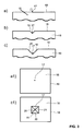
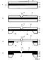
- the alignment process to get the nanowires 4 parallel to the substrate 1 is based on the mechanical force exerted on the nanowires 4 and the resulting permanent change of the orientation direction of the nanowires 4, as shown schematically in FIGS FIGS. 1c) -d) is shown.
- An aid 5 having a certain geometry is used to exert a force on the nanowires 4, so that the nanowires 4, which are not oriented parallel to the substrate 1, lie flat on the substrate 1 after the application of force, i. parallel to its surface 2, lie.
- a (vectorial) component of the force must act perpendicularly in the direction of substrate 1. This force may be applied across a flat or curved surface of a secondary substrate 5.
- the nanowires are all simultaneously pressed onto the substrate (sandwich). In the case of a curved surface, the nanowires are sequentially pressed onto the substrate (as in a rolling pin / rolling pin). A bullet over that Substrate rolls is also possible.
- the nanowires 4 remain immobilized on the substrate, presumably essentially due to van der Waals forces.
- a special adhesive surface functionalization on substrate and nanowires can make the process more efficient. For example, the use of an adhesive that does not adhere to the device, but firmly connects nanowires and substrate together.
- a special anti-adhesion coating may be provided on the tool 5, which has fewer interactions with the nanowires 4 than the substrate 1 on which the nanowires 4 are to be immobilized.
- the process works in many cases without adhesive or anti-adhesive coating of the tool 5.
- a mask aligner (otherwise used for lithography) was used as a technical apparatus that allows the nanowire substrate to be pressed from below against a quartz glass sheet (tool 5).
- Such an apparatus is particularly suitable because there is no (or very little) lateral displacement between the nanowire substrate and quartz glass sheet during approach and removal. If the diameter of the initial catalyst deposition surface 9 is small, in relation to the length of the nanowires, then the nanowires are oriented radially to the location of the catalyst surface 2 after the alignment process, as shown for example by Figure 2c ) can be recognized.
- the electrodes 11-14 can be produced by lithography and electron beam metal evaporation and subsequent lift-off process.
- the gold catalysts (5-50 nm) are applied to a substrate 1, which can withstand the process temperatures of 465 ° C selected here.
- the substrates 1 can for the proposed applications silicon, silicon dioxide, or conventional glass.
- the substrates 1 are placed in an oven, which is normally used for vapor deposition. This is in this case an externally heated quartz glass tube, in which the internal pressure can be precisely controlled.
- a gas mixture of silane and hydrogen is added to the process chamber.
- Disilane and other silicon-containing gases are also possible (SiH 4 , Si 2 H 6 ).
- the pressure is reduced to 5 millibars during the process. Since the silicon-containing gas is consumed during the process, a continuous flow of gas through the process chamber is ensured.
- the gas quantities for the particular process are: 100 sccm (standard cubic centimeter) silane and 200 sccm hydrogen.
- Hydrogen is a carrier gas which has no direct chemical catalytic function and can be replaced by another gas such as nitrogen.
- the process also works with pure silane, or in the presence of other inert gases.
- the process time is typically 30-60 minutes, with the process duration being directly proportional to the length of the resulting nanowires 4.
- the wires grow over the process time with a presumably substantially constant growth rate.
- the given parameters give a growth rate of about 10-20 microns per hour.
- the diameter of the nanowires corresponds approximately to the size of the gold particles (5-50 nm).
- At the beginning of the process there is a lag phase during which there is essentially no growth. The growth does not start until after a few minutes (presumably first activation and saturation of the catalyst particles until the ideal eutectic mixture for growth between gold and silicon has formed).
- the silane pressure (or partial pressure in the presence of other gases) and the temperature determine the growth rate. Higher pressure, as well as higher temperatures lead to faster growth.
- the uncatalytic deposition of silicon from silane gas begins at approx. 470 ° C and is relatively substrate independent.
- Typical parameters Substrate: SiO2 / glass; Catalysts: gold nanoparticles (5-50 nm); Process temperature: 465 ° C; Process time: 30-60 minutes; Gas flow: 100 sccm silane, 200 sccm hydrogen; Total pressure: 5 mbar.
- the present invention further relates to a dry chemical method of surface processing monocrystalline substrates.
- This method is now intended in particular with the aid of FIG. 3 will be described in detail in the context of experimental regulations.
- the process for the lithography-free production of pyramidal recesses in monocrystalline silicon by means of a new dry chemical etching process can be carried out as follows:
- a gold layer is applied in a high vacuum by means of electron beam metal evaporation.
- the nominal layer thickness is 0.1-2.0 nanometers.
- the small nominal layer thickness leads to the fact that no closed gold film is formed, but that nanometer-sized gold (Au) clusters 17 form on the silicon surface 18 (cf. FIG. 3 a) .
- Other methods of applying Au nanoparticles 17 to the process may also be suitable, for example, processes as described above in the context of the first aspect of the invention.
- the different surface energy between gold and silicon is responsible for the formation of Au nanoparticles 17. (On SiO 2, for example, with the same nominal layer thickness, the particles become about 2-5 times as large as on Si).
- the silicon wafer 16 with the applied gold particles 17 is heated at 950 ° C at atmospheric pressure in a quartz tube furnace under a nitrogen atmosphere or other inert gas (it is only an oxidation of the silicon to prevent).
- Atomic small square depressions 19 are initially formed which grow proportionally in their dimensions over the process time (cf. FIG. 3 b) ,
- the process time defines the size / depth of the pyramidal recesses 19.
- the recesses After 30 minutes at 950 °, the recesses have a diameter of about 200 nm.
- the depth corresponds to the flanks of the recesses lowered below 57.x °, corresponding to the pyramidal shape.
- the silicon surface has been homogeneously vaporized with metal, and thus the gold nanoparticles 17 have a very high density (number per area), the etched depressions form in a much smaller number per unit area.
- the excess gold can be removed by means of potassium iodide or other gold-solubilizing processes (e.g., aqua regia).
- SOI Silicon on Insulator.
- An SOI wafer 23 is a conventional silicon wafer of normal thickness. however On the one side of the wafer there are a thin silicon oxide layer 22 and above it another thin monocrystalline silicon layer 21. In this arrangement, the oxide 22 is located between the wafer 23 and the thin silicon layer 21. Suitable dimensions for the layer thicknesses are:
- the thickness of the underlying oxide layer plays a minor role. It must preferably be thick enough to stop the Au etch as an etch barrier (typically> 5-10 nm).
- the dry chemical etching process described above is now carried out on the SOI wafer.
- the dimenions, in particular the depth of the pyramidal recesses 19, are aimed at (over the process time at 950 °) such that the depth of the resulting holes / pyramids (the geometric pyramid defined by the boundary surfaces) would be a non-zero number of nanometers lower , as the top silicon layer has thickness.
- the size of the plateau can be set very accurately. This is done via the difference between the nominal pyramid depth and the existing thickness of the silicon top layer 21.
- the SOI wafer can now be patterned from the underside by means of conventional wet-chemical etching processes in such a way that the underlying thick silicon layer and likewise the SiO 2 layer are removed (compare illustrations according to FIGS FIG. 4 b) -e) and corresponding more detailed description below).
- Only the original silicon top layer 21 then remains as a free-floating membrane. Silicon is removed via potassium hydroxide solution and the SiO 2 layer via hydrofluoric acid.
- the silicon top layer is protected for this purpose by means of a potassium hydroxide and HF-resistant protective film made of a polymer material. Where the pyramid-shaped depressions (at their lowest point) possessed the plateau of SiO 2 , the size of the plateau is now correspondingly large. (Pore / hole / aperture).
- the Si 23 and the SiO 2 layer 22 on the underside of the SOI wafer can also be structured (locally) removed so that the majority of the wafer serves as mechanical support for the free-floating thin silicon top layer 21.
- the underside of the wafer is patterned for this purpose with optical lithography.
- the openings in The photoresist may be several microns to several millimeters in size, depending on the size / area requirement of the free-floating and funneled thin silicon membrane.
- the present invention also relates to a method of manufacturing a sensor element, which preferably makes use of the methods described above for producing a nanowire or for producing a funnel-shaped hole in a silicon membrane.
- a nanowire for example, a CNT can be used, and the funnel-shaped opening can also be produced using a wet-chemical method in the silicon membrane.
- the production process is to be continued with the help of FIG. 4 a) -k) and the mode of operation with the aid of Figure 4l ) -M).
- Nanowire sensor with nano-funnels for the analysis of long-chain molecules, sensor geometry and the mode of operation (cf. FIG. 4 ):
- the sensor consists of an electrically contacted silicon nanowire 4 or a carbon nanotube (CNT), which is located on an insulating substrate (an insulating membrane 18/29). Beneath the nanowire 4 (or CNT) is a nanotube 19 which presents an opening in the substrate / membrane to the bottom.
- the molecules to be analyzed 35 are long-chain polymers / polypeptides, which are composed of different subunits (proteins / DNA).
- the electrical sensitivity of the nanowire 4 (CNT) makes it possible to detect the individual subunits of the long-chain molecule 35 in direct physical contact between the two and measure them electronically via the nanowire / CNT 4. For sequencing all subunits, the molecule is pulled lengthwise across the nanowire / CNT 4, sequentially providing the electrical information corresponding to each molecular building block.
- the nanowire / CNT 4 can be specifically chemically functionalized to create a stronger interaction between the individual subunits and the nanowire 4, thereby amplifying the signals of the individual molecular building blocks.
- the complementary base pairs can be applied to the nanowires / CNTs to create a larger electrical signal through the binding.
- the special geometry of the nanowire sensor with a funnel over a membrane allows the molecule to be positioned precisely above the nanowire and to exert precisely directed tensile forces / speeds with a well-defined deflection of the molecule across the nanowire / CNT.
- the molecules 35 are functionalized at one end with a polymer bead 36 which is 0.5-10 microns in diameter, so it will not through the funnel 19 fits.
- the polymer bead 36 serves to move the individual molecules by means of an optical trap, or in the case of a magnetic bead with a magnetic trap, and to position them over the hopper 19 (Optical Trap, with which small objects in liquid can move).
- DNA can e.g. specifically be chemically connected at the respective ends with a variety of objects / polymer beads.
- the strong negative electrical charge 38 of the DNA allows the molecule to move to the bottom, i. from the liquid region 33 into the liquid region 34 along the direction 39 shown schematically through the hopper 19 to draw. This is done by means of an electrical potential between the liquid portions 33/34 on the top and bottom of the diaphragm 29, in which the funnel opening 19 is located.
- the electrostatic potential is generated via electrodes in the liquid in each case above and below the insulating membrane 29. The molecule 35 would be pulled through the funnel opening without the polymer bead.
- the molecule now experiences an electrostatic pulling force 39 to the bottom: This force is aligned perpendicular to the membrane.
- a lateral tensile force can now be exerted on the molecule 35 via the polymer bead 36, which force is directed counter to the electrostatic tensile force 39.
- the molecule 35 is stretched and exerts a mechanical force on the same by the deflection around the nanowire.
- the molecule is exactly fixed in position relative to the wire 4.
- the speed of traversing can be precisely controlled and reversibly switched back and forth in both directions. This allows multiple readings to reduce the measurement noise.
- optical devices which consist of a single laser source by means of.
- Battery optic beam splitters can position and move up to hundreds of optical traps on a substrate independently of each other. This allows a parallel operation of several sensors on a substrate realize (parallel DNA sequencing).
- the areas on which the funnels 19 are to be located are defined on the top silicon layer 21.
- the nominal layer thickness of 0.5 nm gold is evaporated, resulting in the layer 9 in clearly defined areas on the surface 18.
- the heating process at 950 ° C and the corresponding time provides the nanotube 19.
- the silicon wafer is removed from the bottom by means of potassium hydroxide solution and the SiO 2 layer etched away by means of hydrofluoric acid.
- the now freely floating silicon membrane 21 is converted into layer 29 in electrically insulating SiO 2 in a thermal oxidation step.
- the surfaces are now defined at the desired locations by means of optical lithography, on which the gold catalyst particles 3 should lie to the growth of the nanowires 4.
- the areas for the nanowire growth are located directly next to the areas on which the nanotubes 19 were generated.
- the nanowire growth process is performed as described separately.
- the unaligned nanowires 4 are immobilized laterally onto the substrate 29 via the folding method. Part of the nanowires 4 will be as desired over the Nano-funnel 19 are, a certain proportion, however, not.
- the distribution of well positioned nanowires over funnels is statistical and can be varied to some extent depending on nanowire density and funnel density. However, this is not a problem, because the input opening of the funnel is sufficiently large (see also FIG. 5 ). Due to the large number of components 19/4 which can be produced in parallel on a substrate 29, a relatively low yield of well-positioned nanowires 4 is sufficient to achieve a sufficiently large number of well-positioned nanowires 4 on a chip.
- the laterally positioned nanowires 4 are then contacted with metal electrodes 30 via optical lithography.
- the metal electrodes 30 In order to operate the sensor assembly in an electrolytic liquid 33/34, the metal electrodes 30 must be electrically isolated from the environment.
- the metal electrodes 30 are coated with an electrically insulating layer 31 of SiO 2 or silicon nitride, wherein the nanowires 4 remain free (also by means of optical lithography).
- the arrangement is embedded in a microscope-compatible chamber, so that two separate liquid reservoirs 33/34 are formed, which are connected to each other only through the holes 19 of the membranes 29.
- the separate reservoirs 33/34 there are additional electrodes to apply the electrostatic force to the DNA molecules and to pull them through the funnels 19.
- the beads 36 can be positioned with the DNA 35 via the appropriate sensors to pull the DNA 35 along the nanowires 4 and read electrically.
Landscapes
- Engineering & Computer Science (AREA)
- Chemical & Material Sciences (AREA)
- Health & Medical Sciences (AREA)
- Life Sciences & Earth Sciences (AREA)
- Physics & Mathematics (AREA)
- Biomedical Technology (AREA)
- Crystallography & Structural Chemistry (AREA)
- General Physics & Mathematics (AREA)
- Analytical Chemistry (AREA)
- Nanotechnology (AREA)
- Materials Engineering (AREA)
- Metallurgy (AREA)
- Organic Chemistry (AREA)
- Manufacturing & Machinery (AREA)
- General Health & Medical Sciences (AREA)
- Pathology (AREA)
- Biochemistry (AREA)
- Immunology (AREA)
- Microelectronics & Electronic Packaging (AREA)
- Biophysics (AREA)
- Medicinal Chemistry (AREA)
- Molecular Biology (AREA)
- Hematology (AREA)
- Food Science & Technology (AREA)
- Urology & Nephrology (AREA)
- Condensed Matter Physics & Semiconductors (AREA)
- Spectroscopy & Molecular Physics (AREA)
- Computer Hardware Design (AREA)
- Chemical Kinetics & Catalysis (AREA)
- Electrochemistry (AREA)
- Crystals, And After-Treatments Of Crystals (AREA)
- Investigating Or Analyzing Materials By The Use Of Electric Means (AREA)
- Micromachines (AREA)
- Catalysts (AREA)
Priority Applications (7)
| Application Number | Priority Date | Filing Date | Title |
|---|---|---|---|
| EP11006842A EP2562135A1 (fr) | 2011-08-22 | 2011-08-22 | Procédé de fabrication et d'alignement de nanofils et applications d'un tel procédé |
| PCT/EP2012/003530 WO2013026561A1 (fr) | 2011-08-22 | 2012-08-20 | Procédé de fabrication et d'orientation de nanofils et applications d'un tel procédé |
| CN201280051913.5A CN103958397B (zh) | 2011-08-22 | 2012-08-20 | 用于制造和对准纳米线的方法和这种方法的应用 |
| KR1020147007552A KR102027995B1 (ko) | 2011-08-22 | 2012-08-20 | 나노와이어의 제조 및 정렬을 위한 방법 및 이와 같은 방법의 적용 |
| EP12750327.4A EP2748107B1 (fr) | 2011-08-22 | 2012-08-20 | Procédé de fabrication et d'orientation de nanofils et applications d'un tel procédé |
| JP2014526413A JP6092871B2 (ja) | 2011-08-22 | 2012-08-20 | ナノワイヤの製造及び整列方法、及びその方法の応用 |
| US14/240,265 US9366643B2 (en) | 2011-08-22 | 2012-08-20 | Method for producing and aligning nanowires and applications of such a method |
Applications Claiming Priority (1)
| Application Number | Priority Date | Filing Date | Title |
|---|---|---|---|
| EP11006842A EP2562135A1 (fr) | 2011-08-22 | 2011-08-22 | Procédé de fabrication et d'alignement de nanofils et applications d'un tel procédé |
Publications (1)
| Publication Number | Publication Date |
|---|---|
| EP2562135A1 true EP2562135A1 (fr) | 2013-02-27 |
Family
ID=46724329
Family Applications (2)
| Application Number | Title | Priority Date | Filing Date |
|---|---|---|---|
| EP11006842A Withdrawn EP2562135A1 (fr) | 2011-08-22 | 2011-08-22 | Procédé de fabrication et d'alignement de nanofils et applications d'un tel procédé |
| EP12750327.4A Active EP2748107B1 (fr) | 2011-08-22 | 2012-08-20 | Procédé de fabrication et d'orientation de nanofils et applications d'un tel procédé |
Family Applications After (1)
| Application Number | Title | Priority Date | Filing Date |
|---|---|---|---|
| EP12750327.4A Active EP2748107B1 (fr) | 2011-08-22 | 2012-08-20 | Procédé de fabrication et d'orientation de nanofils et applications d'un tel procédé |
Country Status (6)
| Country | Link |
|---|---|
| US (1) | US9366643B2 (fr) |
| EP (2) | EP2562135A1 (fr) |
| JP (1) | JP6092871B2 (fr) |
| KR (1) | KR102027995B1 (fr) |
| CN (1) | CN103958397B (fr) |
| WO (1) | WO2013026561A1 (fr) |
Cited By (3)
| Publication number | Priority date | Publication date | Assignee | Title |
|---|---|---|---|---|
| CN113247859A (zh) * | 2021-05-13 | 2021-08-13 | 北京理工大学 | 一种基于飞秒激光的裂纹式纳米缝隙结构制备方法 |
| CN113759152A (zh) * | 2021-08-06 | 2021-12-07 | 三峡大学 | 磁场控制的磁性纳米线的测量方法 |
| EP4081794A4 (fr) * | 2019-12-23 | 2024-01-10 | Nanodx Inc | Système de capteur et procédés |
Families Citing this family (18)
| Publication number | Priority date | Publication date | Assignee | Title |
|---|---|---|---|---|
| US9784802B1 (en) | 2012-04-11 | 2017-10-10 | Louisiana Tech Research Corporation | GMR nanowire sensors |
| US9103654B1 (en) * | 2012-04-11 | 2015-08-11 | Louisiana Tech University Research Foundation, A Division Of Louisiana Tech University Foundation, Inc. | GMR nanowire sensors |
| US10718636B1 (en) | 2012-04-11 | 2020-07-21 | Louisiana Tech Research Corporation | Magneto-resistive sensors |
| DE102014112597B4 (de) | 2013-09-03 | 2016-10-06 | Electronics And Telecommunications Research Institute | Vibrationsvorrichtung und Verfahren zur Herstellung einer Vibrationsvorrichtung |
| FR3019188B1 (fr) * | 2014-03-27 | 2017-11-24 | Commissariat Energie Atomique | Procede de croissance d'un element allonge a partir d'un germe forme dans un creux d'une couche ou d'un plot de nucleation |
| CN104296799B (zh) | 2014-10-30 | 2016-08-24 | 京东方科技集团股份有限公司 | 微型传感器本体及其制造方法、微型传感器 |
| JP6283305B2 (ja) * | 2014-12-04 | 2018-02-21 | 株式会社日立ハイテクノロジーズ | 生体分子測定装置及び生体分子測定方法 |
| US9443865B2 (en) * | 2014-12-18 | 2016-09-13 | Sandisk Technologies Llc | Fabricating 3D NAND memory having monolithic crystalline silicon vertical NAND channel |
| CN109155354A (zh) * | 2016-02-09 | 2019-01-04 | 罗斯韦尔生物技术股份有限公司 | 电子无标签的dna和基因组测序 |
| US10416147B2 (en) | 2016-03-18 | 2019-09-17 | Hitachi, Ltd. | Method of manufacturing membrane device, membrane device, and nanopore device |
| KR102007428B1 (ko) * | 2017-03-09 | 2019-08-05 | 코닝 인코포레이티드 | 글라스 지지체에 의하여 지지되는 금속 박막의 제조방법 |
| US10830756B2 (en) * | 2017-09-22 | 2020-11-10 | Applied Materials, Inc. | Method to create a free-standing membrane for biological applications |
| US11119066B2 (en) * | 2018-06-05 | 2021-09-14 | King Fahd University Of Petroleum And Minerals | Room temperature nitrogen dioxide gas sensor |
| CN112512959A (zh) * | 2018-08-09 | 2021-03-16 | Lpkf激光电子股份公司 | 用于制造微结构的方法 |
| CN113710999A (zh) * | 2019-04-17 | 2021-11-26 | 威卡亚力山大维甘德欧洲两合公司 | 用于检测压力和/或料位和/或流量和/或密度和/或质量和/或温度的传感器 |
| US11543429B2 (en) * | 2019-04-25 | 2023-01-03 | Morgan State University | Nanoscale scanning electrochemical microscopy electrode method |
| CN112018032A (zh) * | 2019-05-13 | 2020-12-01 | 京东方科技集团股份有限公司 | 一种阵列基板、其制备方法及显示面板 |
| CN113415780B (zh) * | 2021-06-18 | 2024-01-30 | 合肥工业大学 | 一种一维有序结构的金属氧化物纳米纤维薄膜材料及其制备方法 |
Citations (3)
| Publication number | Priority date | Publication date | Assignee | Title |
|---|---|---|---|---|
| US20050181587A1 (en) * | 2002-09-30 | 2005-08-18 | Nanosys, Inc. | Large-area nanoenabled macroelectronic substrates and uses therefor |
| WO2007136755A2 (fr) * | 2006-05-19 | 2007-11-29 | Massachusetts Institute Of Technology | Traitement en continu pour la production de nanostructures y compris des nanotubes |
| US20080224122A1 (en) * | 2004-12-28 | 2008-09-18 | Tohru Saitoh | Semiconductor Nanowire and Semiconductor Device Including the Nanowire |
Family Cites Families (12)
| Publication number | Priority date | Publication date | Assignee | Title |
|---|---|---|---|---|
| US20060175601A1 (en) * | 2000-08-22 | 2006-08-10 | President And Fellows Of Harvard College | Nanoscale wires and related devices |
| US6863833B1 (en) * | 2001-06-29 | 2005-03-08 | The Board Of Trustees Of The Leland Stanford Junior University | Microfabricated apertures for supporting bilayer lipid membranes |
| US7282130B2 (en) * | 2003-01-31 | 2007-10-16 | Agilent Technologies, Inc. | Apparatus and method for control of biopolymer translocation through a nanopore |
| US7067328B2 (en) * | 2003-09-25 | 2006-06-27 | Nanosys, Inc. | Methods, devices and compositions for depositing and orienting nanostructures |
| ATE529734T1 (de) * | 2005-04-06 | 2011-11-15 | Harvard College | Molekulare charakterisierung mit kohlenstoff- nanoröhrchen-steuerung |
| TWI287041B (en) * | 2005-04-27 | 2007-09-21 | Jung-Tang Huang | An ultra-rapid DNA sequencing method with nano-transistors array based devices |
| KR100842886B1 (ko) * | 2006-04-04 | 2008-07-02 | 재단법인서울대학교산학협력재단 | 나노선을 이용한 식품 첨가물 l-글루타민산나트륨 검출용바이오센서 및 이의 제조 방법 |
| US7892610B2 (en) * | 2007-05-07 | 2011-02-22 | Nanosys, Inc. | Method and system for printing aligned nanowires and other electrical devices |
| CN102072931B (zh) * | 2010-12-09 | 2013-07-17 | 华东师范大学 | 一种基于硅纳米线的生物传感器制备方法及在dna检测中的应用 |
| CN102129981B (zh) * | 2010-12-30 | 2013-06-05 | 北京大学深圳研究生院 | 一种纳米线及纳米线晶体管的制作方法 |
| CN102142376B (zh) * | 2010-12-31 | 2015-12-09 | 上海集成电路研发中心有限公司 | 硅纳米线围栅器件的制备方法 |
| CN102157371B (zh) * | 2011-03-23 | 2012-08-22 | 北京大学 | 一种制作单晶硅纳米结构的方法 |
-
2011
- 2011-08-22 EP EP11006842A patent/EP2562135A1/fr not_active Withdrawn
-
2012
- 2012-08-20 EP EP12750327.4A patent/EP2748107B1/fr active Active
- 2012-08-20 KR KR1020147007552A patent/KR102027995B1/ko active IP Right Grant
- 2012-08-20 CN CN201280051913.5A patent/CN103958397B/zh active Active
- 2012-08-20 JP JP2014526413A patent/JP6092871B2/ja active Active
- 2012-08-20 WO PCT/EP2012/003530 patent/WO2013026561A1/fr active Application Filing
- 2012-08-20 US US14/240,265 patent/US9366643B2/en active Active
Patent Citations (3)
| Publication number | Priority date | Publication date | Assignee | Title |
|---|---|---|---|---|
| US20050181587A1 (en) * | 2002-09-30 | 2005-08-18 | Nanosys, Inc. | Large-area nanoenabled macroelectronic substrates and uses therefor |
| US20080224122A1 (en) * | 2004-12-28 | 2008-09-18 | Tohru Saitoh | Semiconductor Nanowire and Semiconductor Device Including the Nanowire |
| WO2007136755A2 (fr) * | 2006-05-19 | 2007-11-29 | Massachusetts Institute Of Technology | Traitement en continu pour la production de nanostructures y compris des nanotubes |
Non-Patent Citations (3)
| Title |
|---|
| ALBUSCHIES, J., M. BAUS, O. WINKLER, B. HADAM, B. SPANGENBERG, H. KURZ: "High-density silicon nanowire growth from self-assembled Au nanoparticles", MICROELECTRONIC ENGINEERING, vol. 83, no. 4-9, 2006, pages 1530 - 1533 |
| YI-KUEI CHANG ET AL: "The fabrication of ZnO nanowire field-effect transistors by roll-transfer printing", NANOTECHNOLOGY, IOP, BRISTOL, GB, vol. 20, no. 19, 13 May 2009 (2009-05-13), pages 195302, XP020152941, ISSN: 0957-4484, DOI: 10.1088/0957-4484/20/19/195302 * |
| ZHIYONG FAN ET AL: "Wafer-Scale Assembly of Highly Ordered Semiconductor Nanowire Arrays by Contact Printing", NANO LETTERS, vol. 8, no. 1, 1 January 2008 (2008-01-01), pages 20 - 25, XP055017384, ISSN: 1530-6984, DOI: 10.1021/nl071626r * |
Cited By (4)
| Publication number | Priority date | Publication date | Assignee | Title |
|---|---|---|---|---|
| EP4081794A4 (fr) * | 2019-12-23 | 2024-01-10 | Nanodx Inc | Système de capteur et procédés |
| CN113247859A (zh) * | 2021-05-13 | 2021-08-13 | 北京理工大学 | 一种基于飞秒激光的裂纹式纳米缝隙结构制备方法 |
| CN113759152A (zh) * | 2021-08-06 | 2021-12-07 | 三峡大学 | 磁场控制的磁性纳米线的测量方法 |
| CN113759152B (zh) * | 2021-08-06 | 2024-03-12 | 三峡大学 | 磁场控制的磁性纳米线的测量方法 |
Also Published As
| Publication number | Publication date |
|---|---|
| JP6092871B2 (ja) | 2017-03-08 |
| KR20140097114A (ko) | 2014-08-06 |
| CN103958397A (zh) | 2014-07-30 |
| EP2748107B1 (fr) | 2018-08-15 |
| US9366643B2 (en) | 2016-06-14 |
| JP2014531327A (ja) | 2014-11-27 |
| WO2013026561A1 (fr) | 2013-02-28 |
| US20140285224A1 (en) | 2014-09-25 |
| KR102027995B1 (ko) | 2019-10-02 |
| EP2748107A1 (fr) | 2014-07-02 |
| CN103958397B (zh) | 2017-12-22 |
Similar Documents
| Publication | Publication Date | Title |
|---|---|---|
| EP2748107B1 (fr) | Procédé de fabrication et d'orientation de nanofils et applications d'un tel procédé | |
| DE4126151C2 (de) | Ausleger für ein Scansondenmikroskop und ein Verfahren zu dessen Herstellung | |
| EP2032501B1 (fr) | Nanomicrophone ou nanocapteur de pression | |
| DE102007014880A1 (de) | Kohlenstoffnanoröhrchenkette und Herstellungsverfahren dafür, Zieldetektor und Zieldetektionsverfahren | |
| EP1379862B1 (fr) | Paire d'electrodes de mesure, biodetecteur comportant une telle paire d'electrodes de mesure et procede de production de cette derniere | |
| DE10332725A1 (de) | Verfahren zur selbstjustierenden Verkleinerung von Strukturen | |
| DE112016005255B4 (de) | Biomolekülmesseinrichtung | |
| EP1225216A1 (fr) | Appareil pour analyser des canaux ioniques dans un membrane | |
| EP3213068A1 (fr) | Composant basé sur un substrat structurable muni d'une structure de membrane tridimensionnelle présentant des pores dans une plage nanométrique, et procédé relevant de la technologie des semi-conducteurs pour la fabrication dudit composant | |
| EP1359593A1 (fr) | Capteur pour la SPM et procedé pour sa fabrication | |
| Francioso et al. | Top-down contact lithography fabrication of a TiO2 nanowire array over a SiO2 mesa | |
| EP1803148A1 (fr) | Procede de fabrication de structures a l'echelle du sous-micron | |
| DE69817452T2 (de) | Verfahren zur Herstellung einer micromechanischen Messsonde, insbesondere eines Rasterkraftmikroskops | |
| KR101080612B1 (ko) | 전기화학적 에칭을 위한 식각 구멍 형성 방법 | |
| DE19930104C1 (de) | Verfahren zur Herstellung einer Elektrodenanordnung | |
| EP0622608A1 (fr) | Appareil de balayage pour l'examen de structures de surfaces avec une résolution de l'ordre de microns et procédé pour sa fabrication | |
| JP5196602B2 (ja) | ナノギャップ電極の製造方法 | |
| CN105923621B (zh) | 一种利用电子束诱导淀积制备纳米管道的方法 | |
| EP1716070B1 (fr) | Detecteur micromecanique | |
| JP2006231432A (ja) | ナノギャップ電極の製造方法 | |
| DE19509903A1 (de) | Verfahren zur Herstellung einer Abtastvorrichtung zur kombinierten Untersuchung von verschiedenen Oberflächeneigenschaften mit Auflösung im Nanometerbereich | |
| KR101581783B1 (ko) | 나노유체 채널을 기반으로 하는 채널 구조물 및 이를 제조하는 방법 | |
| EP1209689B1 (fr) | Procédé de fabrication de sondes à balayage intégrées | |
| DE19841125A1 (de) | Verfahren und Anordnung zur Beweglichkeitseinschränkung von lebenden Zellen | |
| Yau | IC Compatible Wafer Level Fabrication of Silicon Nanowire Field Effect Transistors for Biosensing Applications |
Legal Events
| Date | Code | Title | Description |
|---|---|---|---|
| PUAI | Public reference made under article 153(3) epc to a published international application that has entered the european phase |
Free format text: ORIGINAL CODE: 0009012 |
|
| AK | Designated contracting states |
Kind code of ref document: A1 Designated state(s): AL AT BE BG CH CY CZ DE DK EE ES FI FR GB GR HR HU IE IS IT LI LT LU LV MC MK MT NL NO PL PT RO RS SE SI SK SM TR |
|
| AX | Request for extension of the european patent |
Extension state: BA ME |
|
| STAA | Information on the status of an ep patent application or granted ep patent |
Free format text: STATUS: THE APPLICATION IS DEEMED TO BE WITHDRAWN |
|
| 18D | Application deemed to be withdrawn |
Effective date: 20130828 |