EP2540862A1 - Kohlenstofffilmbeschichtung - Google Patents
Kohlenstofffilmbeschichtung Download PDFInfo
- Publication number
- EP2540862A1 EP2540862A1 EP11747486A EP11747486A EP2540862A1 EP 2540862 A1 EP2540862 A1 EP 2540862A1 EP 11747486 A EP11747486 A EP 11747486A EP 11747486 A EP11747486 A EP 11747486A EP 2540862 A1 EP2540862 A1 EP 2540862A1
- Authority
- EP
- European Patent Office
- Prior art keywords
- single crystal
- graphene
- copper
- thin film
- substrate
- Prior art date
- Legal status (The legal status is an assumption and is not a legal conclusion. Google has not performed a legal analysis and makes no representation as to the accuracy of the status listed.)
- Granted
Links
Images


Classifications
-
- B—PERFORMING OPERATIONS; TRANSPORTING
- B82—NANOTECHNOLOGY
- B82Y—SPECIFIC USES OR APPLICATIONS OF NANOSTRUCTURES; MEASUREMENT OR ANALYSIS OF NANOSTRUCTURES; MANUFACTURE OR TREATMENT OF NANOSTRUCTURES
- B82Y30/00—Nanotechnology for materials or surface science, e.g. nanocomposites
-
- C—CHEMISTRY; METALLURGY
- C01—INORGANIC CHEMISTRY
- C01B—NON-METALLIC ELEMENTS; COMPOUNDS THEREOF; METALLOIDS OR COMPOUNDS THEREOF NOT COVERED BY SUBCLASS C01C
- C01B32/00—Carbon; Compounds thereof
- C01B32/05—Preparation or purification of carbon not covered by groups C01B32/15, C01B32/20, C01B32/25, C01B32/30
-
- C—CHEMISTRY; METALLURGY
- C01—INORGANIC CHEMISTRY
- C01B—NON-METALLIC ELEMENTS; COMPOUNDS THEREOF; METALLOIDS OR COMPOUNDS THEREOF NOT COVERED BY SUBCLASS C01C
- C01B32/00—Carbon; Compounds thereof
- C01B32/15—Nano-sized carbon materials
- C01B32/182—Graphene
- C01B32/184—Preparation
- C01B32/186—Preparation by chemical vapour deposition [CVD]
-
- C—CHEMISTRY; METALLURGY
- C01—INORGANIC CHEMISTRY
- C01B—NON-METALLIC ELEMENTS; COMPOUNDS THEREOF; METALLOIDS OR COMPOUNDS THEREOF NOT COVERED BY SUBCLASS C01C
- C01B32/00—Carbon; Compounds thereof
- C01B32/15—Nano-sized carbon materials
- C01B32/182—Graphene
- C01B32/184—Preparation
- C01B32/19—Preparation by exfoliation
-
- C—CHEMISTRY; METALLURGY
- C01—INORGANIC CHEMISTRY
- C01B—NON-METALLIC ELEMENTS; COMPOUNDS THEREOF; METALLOIDS OR COMPOUNDS THEREOF NOT COVERED BY SUBCLASS C01C
- C01B32/00—Carbon; Compounds thereof
- C01B32/50—Carbon dioxide
-
- C—CHEMISTRY; METALLURGY
- C23—COATING METALLIC MATERIAL; COATING MATERIAL WITH METALLIC MATERIAL; CHEMICAL SURFACE TREATMENT; DIFFUSION TREATMENT OF METALLIC MATERIAL; COATING BY VACUUM EVAPORATION, BY SPUTTERING, BY ION IMPLANTATION OR BY CHEMICAL VAPOUR DEPOSITION, IN GENERAL; INHIBITING CORROSION OF METALLIC MATERIAL OR INCRUSTATION IN GENERAL
- C23C—COATING METALLIC MATERIAL; COATING MATERIAL WITH METALLIC MATERIAL; SURFACE TREATMENT OF METALLIC MATERIAL BY DIFFUSION INTO THE SURFACE, BY CHEMICAL CONVERSION OR SUBSTITUTION; COATING BY VACUUM EVAPORATION, BY SPUTTERING, BY ION IMPLANTATION OR BY CHEMICAL VAPOUR DEPOSITION, IN GENERAL
- C23C16/00—Chemical coating by decomposition of gaseous compounds, without leaving reaction products of surface material in the coating, i.e. chemical vapour deposition [CVD] processes
- C23C16/02—Pretreatment of the material to be coated
- C23C16/0272—Deposition of sub-layers, e.g. to promote the adhesion of the main coating
- C23C16/0281—Deposition of sub-layers, e.g. to promote the adhesion of the main coating of metallic sub-layers
-
- C—CHEMISTRY; METALLURGY
- C23—COATING METALLIC MATERIAL; COATING MATERIAL WITH METALLIC MATERIAL; CHEMICAL SURFACE TREATMENT; DIFFUSION TREATMENT OF METALLIC MATERIAL; COATING BY VACUUM EVAPORATION, BY SPUTTERING, BY ION IMPLANTATION OR BY CHEMICAL VAPOUR DEPOSITION, IN GENERAL; INHIBITING CORROSION OF METALLIC MATERIAL OR INCRUSTATION IN GENERAL
- C23C—COATING METALLIC MATERIAL; COATING MATERIAL WITH METALLIC MATERIAL; SURFACE TREATMENT OF METALLIC MATERIAL BY DIFFUSION INTO THE SURFACE, BY CHEMICAL CONVERSION OR SUBSTITUTION; COATING BY VACUUM EVAPORATION, BY SPUTTERING, BY ION IMPLANTATION OR BY CHEMICAL VAPOUR DEPOSITION, IN GENERAL
- C23C16/00—Chemical coating by decomposition of gaseous compounds, without leaving reaction products of surface material in the coating, i.e. chemical vapour deposition [CVD] processes
- C23C16/22—Chemical coating by decomposition of gaseous compounds, without leaving reaction products of surface material in the coating, i.e. chemical vapour deposition [CVD] processes characterised by the deposition of inorganic material, other than metallic material
- C23C16/26—Deposition of carbon only
-
- C—CHEMISTRY; METALLURGY
- C30—CRYSTAL GROWTH
- C30B—SINGLE-CRYSTAL GROWTH; UNIDIRECTIONAL SOLIDIFICATION OF EUTECTIC MATERIAL OR UNIDIRECTIONAL DEMIXING OF EUTECTOID MATERIAL; REFINING BY ZONE-MELTING OF MATERIAL; PRODUCTION OF A HOMOGENEOUS POLYCRYSTALLINE MATERIAL WITH DEFINED STRUCTURE; SINGLE CRYSTALS OR HOMOGENEOUS POLYCRYSTALLINE MATERIAL WITH DEFINED STRUCTURE; AFTER-TREATMENT OF SINGLE CRYSTALS OR A HOMOGENEOUS POLYCRYSTALLINE MATERIAL WITH DEFINED STRUCTURE; APPARATUS THEREFOR
- C30B29/00—Single crystals or homogeneous polycrystalline material with defined structure characterised by the material or by their shape
- C30B29/02—Elements
- C30B29/04—Diamond
-
- C—CHEMISTRY; METALLURGY
- C30—CRYSTAL GROWTH
- C30B—SINGLE-CRYSTAL GROWTH; UNIDIRECTIONAL SOLIDIFICATION OF EUTECTIC MATERIAL OR UNIDIRECTIONAL DEMIXING OF EUTECTOID MATERIAL; REFINING BY ZONE-MELTING OF MATERIAL; PRODUCTION OF A HOMOGENEOUS POLYCRYSTALLINE MATERIAL WITH DEFINED STRUCTURE; SINGLE CRYSTALS OR HOMOGENEOUS POLYCRYSTALLINE MATERIAL WITH DEFINED STRUCTURE; AFTER-TREATMENT OF SINGLE CRYSTALS OR A HOMOGENEOUS POLYCRYSTALLINE MATERIAL WITH DEFINED STRUCTURE; APPARATUS THEREFOR
- C30B29/00—Single crystals or homogeneous polycrystalline material with defined structure characterised by the material or by their shape
- C30B29/10—Inorganic compounds or compositions
- C30B29/16—Oxides
- C30B29/20—Aluminium oxides
-
- B—PERFORMING OPERATIONS; TRANSPORTING
- B82—NANOTECHNOLOGY
- B82Y—SPECIFIC USES OR APPLICATIONS OF NANOSTRUCTURES; MEASUREMENT OR ANALYSIS OF NANOSTRUCTURES; MANUFACTURE OR TREATMENT OF NANOSTRUCTURES
- B82Y40/00—Manufacture or treatment of nanostructures
-
- Y—GENERAL TAGGING OF NEW TECHNOLOGICAL DEVELOPMENTS; GENERAL TAGGING OF CROSS-SECTIONAL TECHNOLOGIES SPANNING OVER SEVERAL SECTIONS OF THE IPC; TECHNICAL SUBJECTS COVERED BY FORMER USPC CROSS-REFERENCE ART COLLECTIONS [XRACs] AND DIGESTS
- Y10—TECHNICAL SUBJECTS COVERED BY FORMER USPC
- Y10T—TECHNICAL SUBJECTS COVERED BY FORMER US CLASSIFICATION
- Y10T428/00—Stock material or miscellaneous articles
- Y10T428/30—Self-sustaining carbon mass or layer with impregnant or other layer
-
- Y—GENERAL TAGGING OF NEW TECHNOLOGICAL DEVELOPMENTS; GENERAL TAGGING OF CROSS-SECTIONAL TECHNOLOGIES SPANNING OVER SEVERAL SECTIONS OF THE IPC; TECHNICAL SUBJECTS COVERED BY FORMER USPC CROSS-REFERENCE ART COLLECTIONS [XRACs] AND DIGESTS
- Y10—TECHNICAL SUBJECTS COVERED BY FORMER USPC
- Y10T—TECHNICAL SUBJECTS COVERED BY FORMER US CLASSIFICATION
- Y10T428/00—Stock material or miscellaneous articles
- Y10T428/31504—Composite [nonstructural laminate]
- Y10T428/31678—Of metal
Definitions
- the present invention relates to a large area carbon film laminate for use in electronic devices, transparent conductive films and the like.
- Graphene which is in a form of a flat single layer carbon film composed of sp2-bonded carbon atoms, is expected to be used as a base material such as an ultrahigh performance electronic device and a transparent conductive thin film due to its specifically high electrical conductivity and optical transmittance.
- methods for formation of graphene have been developed, such as a method for peeling from natural graphite, a method for eliminating silicon by a high-temperature heat treatment of silicon carbide, a method for forming graphene on various metal surfaces and the like.
- Non-Patent Literatures 1 and 2 a method for forming a single to several layers of graphene on a surface of a copper foil by a chemical vapor deposition (CVD) method has recently been developed (Non-Patent Literatures 1 and 2).
- the technique of depositing graphene using a copper foil as a base material is performed by a thermal CVD technique.
- a methane gas as a raw material gas is thermally decomposed at approximately 1,000°C to form a single to several layers of graphene on the surface of the copper foil.
- the technique using the copper foil as the base material enables synthesis of graphene with satisfactory utilizing characteristics of a surface of copper, as compared with a conventional technique using other metals such as nickel.
- the graphene obtained by the synthesis method using the copper foil as the base material has a crystal size of several tens of ⁇ m at most right now.
- the graphene to have as large a crystal size as possible, and thus the issue is to increase the crystal size.
- the present invention has been made in view of the above circumstances and an object thereof is to solve a problem such as a small crystal size, which is the issue of a conventional method for formation of a film of graphene by a thermal CVD technique using a copper foil as a substrate, and thus providing a carbon film laminate in which graphene having a larger crystal size is formed.
- the present inventors have intensively studied so as to achieve the above object and found a novel method for obtaining a carbon film laminate in which graphene having a large crystal size is formed, whereby, it is made possible to form graphene with a noticeably larger area as compared with a conventional technique, and thus capable of solving the above issue in the conventional technique.
- the present invention has been accomplished based on these findings and includes the following.
- the carbon film laminate of the present invention in which graphene is deposited on a copper (111) single crystal thin film formed by epitaxial growth on a single crystal substrate, it becomes possible to form graphene having a noticeably larger crystal size (in the 10 mm class) as compared with a conventional one, and thus facilitating the production of ultrahigh performance electronic devices such as a graphene transistor which has hitherto been developed using graphene having a crystal size of several tens of ⁇ m. It also becomes possible to integrate the ultrahigh performance device, and thus a graphene transistor having various performances can be produced.
- Graphene is a flat single layer carbon film composed of sp2-bonded carbon atoms.
- Graphene is described in detail in Non-Patent Literature 1.
- a carbon film laminate of the present invention in which graphene having a large crystal size is deposited is mainly provided based on the employment of specific production conditions.
- a copper (111) single crystal thin film formed by epitaxial growth on a sapphire (0001) single crystal substrate is used as a base material for synthesis of graphene. It is also desired to select the concentration and mole ratio of raw gases, reaction time and the like as the production conditions by a thermal CVD method.
- Non-Patent Literatures 1 and 2 formation of a film of graphene through thermal CVD was performed by the methods disclosed in Non-Patent Literatures 1 and 2 using a copper foil as a base material. Since the copper foil is a polycrystal, its surface is divided into regions each having a different plane direction. Therefore, Raman spectrometry measurement was performed to determine how the thus formed graphene is distributed on a surface of a copper thin film. Furthermore, crystallographic distribution in the plane directions of the surface of the copper foil was determined by electron backscatter diffraction pattern (EBPS).
- EBPS electron backscatter diffraction pattern
- a film of graphene is formed in the regions of Cu (111) plane and Cu (100) plane on a surface of the copper foil, and preferably in the region of Cu (111) plane.
- a film of graphene was scarcely formed in the region of Cu (101) plane of the surface of the copper foil.
- a film of graphene is preferably formed on the crystallographic copper (111) plane.
- the copper surface having the region of Cu (111) plane is used as the base material for formation of a graphene film having a large crystal size.
- single crystal copper having a crystallographic (111) plane is preferably used for formation of a graphene film having a large area.
- a single crystal copper bulk having a crystallographic (111) plane on the surface It is technically possible to prepare a single crystal copper bulk having a crystallographic (111) plane on the surface.
- the single crystal copper bulk is expensive and is unsuited or inappropriate for industrial use.
- a Cu (111) single crystal thin film be formed by epitaxial growth on a single crystal substrate.
- graphene having a large crystal size is obtained by producing a carbon filmlaminate, including a single crystal substrate, a copper (111) single crystal thin film formed by epitaxial growth on the substrate, and graphene deposited on the copper (111) single crystal thin film.
- a single crystal copper thin film having a crystallographic (111) plane in its surface (hereinafter referred to as a "Cu (111) single crystal thin film”) was prepared so as to form a graphene film having a large crystal size.
- the present inventors has found that a Cu (111) single crystal thin film is formed by epitaxial growth on a single crystal substrate by a magnetron sputtering method, by tests of copper single crystal growth on various substrates. Furthermore, graphene having a large crystal size is obtained by producing a carbon film laminate, including a Cu (111) single crystal thin film formed by epitaxial growth on a sapphire (0001) single crystal substrate, and graphene deposited on the Cu (111) single crystal thin film.
- a Cu (111) single crystal thin film is preferably used to form a graphene film having a large crystal size. Since graphene is a two-dimensional crystal composed of a single carbon atom layer, it is considered that its crystal size is largely influenced by flatness of a surface of a Cu (111) single crystal thin film.
- a sapphire (0001) single crystal substrate having a surface composed of terrace surfaces which are flat at the atomic level, and atomic-layer steps, as a substrate for epitaxial growth of a Cu (111) single crystal thin film.
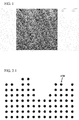
- 1 is an atomic force microscopic image (in a square-shaped area, the side of which being 2 ⁇ m) of the surface of a sapphire (0001) single crystal substrate.
- stripe pattern contrast exists and is composed of terrace surfaces which are flat at the atomic level, and atomic-layer steps, and the stripe pattern contrast is unique to a very flat single crystal surface.
- a sapphire (0001) single crystal substrate having a surface composed of terrace surfaces which are flat at the atomic level, and atomic-layer steps was used as the substrate for epitaxial growth of a Cu (111) single crystal thin film.
- a sapphire (0001) single crystal substrate having a surface composed of terrace surfaces which are flat at the atomic level, and atomic-layer steps was used as the meaning of "single crystal substrate having a surface composed of terrace surfaces which are flat at the atomic level and atomic-layer steps".
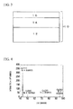
- Fig. 2-1 is a schematic diagram in cross-section of an ordinary crystal surface having poor flatness.
- Fig. 2-2 and Fig. 2-3 are, respectively, a schematic diagram in cross-section of a crystal surface composed of terrace surfaces which are flat at the atomic level, and atomic-layer steps, and a schematic diagram of a crystal surface composed of terrace surfaces which are flat at the atomic level, and atomic-layer steps, as seen from above.
- the broken line (---) indicates an inclination of an actual surface
- the dashed line (- ⁇ - ⁇ -) indicates a crystallographic crystal orientation of a surface.
- the terrace has a width defined by an angle ⁇ between the crystallographic crystal orientation of a surface (- ⁇ - ⁇ -) and an actual inclination of a surface (---).
- graphene having a large crystal size was obtained by forming a carbon film laminate, including a sapphire (0001) single crystal substrate having a surface composed of terrace surfaces which are flat at the atomic level, and atomic-layer steps, a copper (111) single crystal thin film formed by epitaxial growth on the substrate, and graphene deposited on the copper (111) single crystal thin film. Examples will be described in detail below, but the present invention is not intended to be limited thereto.
- Fig. 3 is a schematic diagram illustrating a carbon film laminate according to the present invention.
- the carbon film laminate 10 includes a sapphire (0001) single crystal substrate 12, a copper (111) single crystal thin film 14 formed by epitaxial growth on the substrate 12, and graphene 16 deposited on the copper (111) single crystal thin film.
- the copper (111) single crystal thin film was epitaxially grown on a sapphire (0001) single crystal substrate using a DC magnetron sputtering method.
- the sapphire (0001) single crystal substrate was placed on a substrate stage capable of heating a substrate, and placed in a sputtering system.
- the detailed specifications of a sapphire (0001) single crystal substrate are as follows:
- the sputtering film formation device was evacuated to the pressure of 2.0 ⁇ 10 -4 Pa or less before the substrate for film formation was heated to 100°C and maintained at the temperature. Then, a 1 ⁇ m thick Cu (111) single crystal thin film was formed on a sapphire (0001) single crystal substrate under the conditions of a gas pressure of 1.3 ⁇ 10 -1 Pa and a power of 100 W.
- Detailed film formation conditions are as follows:
- a surface of a sample was irradiated with X-ray at an angle of ⁇ , and on the X-ray detector placed at the angle of double ⁇ (2 ⁇ ) from the X-ray irradiation direction, X-ray intensity emitted from the sample at each 2 ⁇ angle was determined while the angle 2 ⁇ was varied by rotating at every 0.05 degrees between 40 degrees to 100 degrees (in other words, ⁇ was simultaneously varied by rotating at every 0.025 degrees between 20 degrees to 50 degrees).
- This measuring method is generally referred to as 2 ⁇ - ⁇ measurement, which is intended to detect X-ray reflected by a crystal surface parallel to the sample surface.
- a computer programused for the measurement is RINT2000/PC software, Windows (registered trademark) version, manufactured by Rigaku Corporation.
- Fig. 4 is an X-ray diffraction spectrum thus measured.
- X-ray used herein is copper (Cu)-K ⁇ 1 ray. It is apparent that a clear peak exists at 2 ⁇ of 43.4°. This peak is attributed to reflection at Cu (111). Also, a weak peak exists at 2 ⁇ of 95.4°, which is attributed to reflection at Cu (222). If the Cu thin film also has a Cu (200) plane element and a Cu (220) plane element parallel to its surface, corresponding peaks should be observed at 2 ⁇ of 50.6° and 74.3°, respectively, but none of these peaks were observed. The above results revealed that the Cu thin film was composed of a crystal having the (111) plane parallel to its surface and was a (111) single crystal. Thus, it was confirmed that the copper (111) single crystal thin film was epitaxially grown on the sapphire (0001) single crystal substrate.
- graphene was formed by a thermal CVD technique on a surface of a copper (111) single crystal thin film formed by epitaxial growth on a sapphire (0001) single crystal substrate, and thus obtaining a carbon film laminate, as shown in Fig. 3 , including a sapphire (0001) single crystal substrate, a copper (111) single crystal thin film formed by epitaxial growth on the substrate, and graphene deposited on the copper (111) single crystal thin film.
- a heating device required for the thermal CVD technique an infrared gold image furnace capable of performing rapid heating and cooling of the sample and precisely controlling the temperature was used (hereinafter referred to as a furnace).
- the furnace used herein was MINI-LAMP-ANNEALER "MILA3000-P-N" manufactured by Ulvac-Rico Inc. Film formation was performed by the following procedures.
- Fig. 5 illustrates a Raman scattering spectrum thus measured.
- a measurement device is a Model XploRA manufactured by Horiba Ltd., and the measurement was performed under the following conditions: an excitation wavelength of a laser is 632 nm, a spot size of laser beam is 1 micron in diameter, the number of grating lines of a spectroscope is 600 and a measurement time of 5 seconds, and then the measurement was performed twice and the measurement values were accumulated. Measurement was performed in a state where graphene is deposited on a copper (111) single crystal thin film on a sapphire (0001) single crystal substrate.
- Fig. 5 clear peaks were respectively observed at about 2, 670 cm -1 and 1,590 cm -1 of Raman shift, respectively, on a gently-sloping background.
- the peak at about 1,590 cm -1 is attributed to a normal six-membered ring of carbon atoms, which is generally referred to as a G band.
- the peak at about 2,670 cm -1 is generally referred to as a 2D band.
- the gently-sloping background is attributed to fluorescence emitted from a copper thin film of a base material.
- a peak may be sometimes observed at about 1,358 cm -1 and is attributed to a defect of a normal six-membered ring of carbon atoms, and is also referred to as a D band.
- a peak of the D band is not observed, which reveals that graphene produced by the technique of the present invention is a film which is substantially free from defects and has satisfactory crystallinity.
- Non-Patent Literature 1 discloses that when a ratio of the intensity of the 2D band I (2D) to that of the G band I (G) satisfies I (2D) /I (G) ⁇ 2, the film is assumed to be composed of one or two graphene layers. Each background was subtracted from peaks at the 2D band and the G band shown in Fig. 5 , respectively, followed by fitting and further determination of the ratio of intensity by calculation of each area of peaks. As a result, I(2D)/I(G) was 3.27. Accordingly, it was found that the region examined by Raman spectrometry (the region of 1 micron in diameter which is the spot size of measurement laser beam) corresponds to graphene.
- Fig. 7 shows the results of the measurement, in which a white region indicates a region satisfying I(2D)/I(G) ⁇ 2 and a black region indicates a region satisfying I(2D)/I(G) ⁇ 2 or a region where a D band was observed.
- Fig. 8 shows the results of the measurement, in which a white region indicates a region satisfying I (2D) /I (G) ⁇ 2 and a black region indicates a region satisfying I(2D)/I(G) ⁇ 2 or a region where D band was observed.
Applications Claiming Priority (2)
| Application Number | Priority Date | Filing Date | Title |
|---|---|---|---|
| JP2010041419 | 2010-02-26 | ||
| PCT/JP2011/054243 WO2011105530A1 (ja) | 2010-02-26 | 2011-02-25 | 炭素膜積層体 |
Publications (3)
| Publication Number | Publication Date |
|---|---|
| EP2540862A1 true EP2540862A1 (de) | 2013-01-02 |
| EP2540862A4 EP2540862A4 (de) | 2015-12-09 |
| EP2540862B1 EP2540862B1 (de) | 2016-11-23 |
Family
ID=44506928
Family Applications (1)
| Application Number | Title | Priority Date | Filing Date |
|---|---|---|---|
| EP11747486.6A Not-in-force EP2540862B1 (de) | 2010-02-26 | 2011-02-25 | Kohlenstofffilmbeschichtung |
Country Status (7)
| Country | Link |
|---|---|
| US (1) | US9074278B2 (de) |
| EP (1) | EP2540862B1 (de) |
| JP (1) | JP5569825B2 (de) |
| KR (1) | KR101472948B1 (de) |
| CN (1) | CN102859032B (de) |
| ES (1) | ES2615730T3 (de) |
| WO (1) | WO2011105530A1 (de) |
Cited By (4)
| Publication number | Priority date | Publication date | Assignee | Title |
|---|---|---|---|---|
| WO2014189271A1 (ko) * | 2013-05-21 | 2014-11-27 | 한양대학교 산학협력단 | 대면적의 단결정 단일막 그래핀 및 그 제조방법 |
| WO2020053102A1 (en) | 2018-09-10 | 2020-03-19 | Centre National De La Recherche Scientifique | Process for preparing single-crystal thin films |
| CN114604860A (zh) * | 2022-03-15 | 2022-06-10 | 北京石墨烯技术研究院有限公司 | 石墨烯薄膜生长基底及其制备方法和应用 |
| US11913134B2 (en) | 2017-02-02 | 2024-02-27 | Soitec | Process for manufacturing a two-dimensional film of hexagonal crystalline structure using epitaxial growth on a transferred thin metal film |
Families Citing this family (28)
| Publication number | Priority date | Publication date | Assignee | Title |
|---|---|---|---|---|
| EP2458620B1 (de) | 2010-11-29 | 2021-12-01 | IHP GmbH-Innovations for High Performance Microelectronics / Leibniz-Institut für innovative Mikroelektronik | Herstellung von Graphenelektronikbauelementen mittels Stufenoberflächenkontur |
| EP2716601B1 (de) * | 2011-06-02 | 2017-03-15 | JX Nippon Mining & Metals Corporation | Kupferfolie zur graphenherstellung und graphenherstellungsverfahren |
| JP5926035B2 (ja) * | 2011-11-21 | 2016-05-25 | Jx金属株式会社 | グラフェン製造用銅箔及びグラフェン製造用銅箔の製造方法、並びにグラフェンの製造方法 |
| JP5909082B2 (ja) * | 2011-11-21 | 2016-04-26 | Jx金属株式会社 | グラフェン製造用銅箔及びグラフェンの製造方法 |
| US9112002B2 (en) * | 2012-02-13 | 2015-08-18 | Tyco Electronics Corporation | Electrical conductors and methods of manufacturing electrical conductors |
| GB201205801D0 (en) | 2012-03-30 | 2012-05-16 | Isis Innovation | Process |
| JP5918075B2 (ja) * | 2012-08-16 | 2016-05-18 | Jx金属株式会社 | グラフェン製造用圧延銅箔、及びグラフェンの製造方法 |
| KR102083960B1 (ko) * | 2012-08-30 | 2020-03-03 | 엘지전자 주식회사 | 그래핀의 제조 방법 및 그 그래핀과 그 제조 장치 |
| CN103924207B (zh) * | 2013-01-10 | 2017-04-19 | 中国科学院上海微系统与信息技术研究所 | 一种增强泡沫铜在较高温度下抗氧化能力的方法 |
| US10041168B2 (en) * | 2013-01-14 | 2018-08-07 | California Institute Of Technology | Graphene structure |
| CN104995135A (zh) * | 2013-02-19 | 2015-10-21 | Jx日矿日石金属株式会社 | 石墨烯制造用铜箔和石墨烯的制造方法 |
| WO2014128833A1 (ja) * | 2013-02-19 | 2014-08-28 | Jx日鉱日石金属株式会社 | グラフェン製造用銅箔及びグラフェンの製造方法 |
| WO2015126139A1 (en) * | 2014-02-19 | 2015-08-27 | Samsung Electronics Co., Ltd. | Wiring structure and electronic device employing the same |
| KR101541517B1 (ko) * | 2014-03-26 | 2015-08-03 | 부산대학교 산학협력단 | 단결정 구리를 이용한 나노 망사 다층 구조의 투명전극 및 그 제조방법 |
| CN103943601A (zh) * | 2014-05-09 | 2014-07-23 | 浙江大学 | 一种具有铜-石墨烯复相的互连线及其制备方法 |
| WO2015190739A1 (ko) * | 2014-06-09 | 2015-12-17 | 한양대학교 산학협력단 | 수소 원자 또는 수소 이온을 함유하는 단결정 금속막 및 그 제조방법 |
| KR101767242B1 (ko) * | 2014-06-09 | 2017-08-10 | 한양대학교 산학협력단 | 수소 원자 또는 수소 이온을 함유하는 단결정 금속막 및 그 제조방법 |
| CN104045079A (zh) * | 2014-06-25 | 2014-09-17 | 无锡格菲电子薄膜科技有限公司 | 在蓝宝石与外延金属界面外延生长石墨烯的方法 |
| KR101629697B1 (ko) | 2014-10-14 | 2016-06-13 | 한국화학연구원 | 그래핀 적층 구조체의 제조방법 및 이로 제조된 그래핀 적층 구조체 |
| CN104576862B (zh) * | 2014-12-24 | 2017-08-25 | 江苏巨晶新材料科技有限公司 | 一种基于铜衬底的氮化物led垂直芯片及其制备方法 |
| KR101704723B1 (ko) | 2015-04-06 | 2017-02-09 | 연세대학교 산학협력단 | 탄소 박막 소자 및 이의 제조 방법 |
| CN104975344A (zh) * | 2015-07-09 | 2015-10-14 | 中国科学院上海微系统与信息技术研究所 | 基于氧化亚铜薄膜衬底低成核密度石墨烯单晶的制备方法 |
| GB201514542D0 (en) | 2015-08-14 | 2015-09-30 | Thomas Simon C S | A method of producing graphene |
| WO2017034018A1 (ja) * | 2015-08-26 | 2017-03-02 | 並木精密宝石株式会社 | グラフェン膜、複合体、それらの製造方法、及び単結晶サファイア基板 |
| CN106584976A (zh) * | 2016-08-10 | 2017-04-26 | 上海交通大学 | 一种高导电石墨烯/铜基层状复合材料及其制备方法 |
| KR102170111B1 (ko) * | 2018-12-18 | 2020-10-26 | 한양대학교 산학협력단 | 다결정 금속 필름의 비정상입자성장에 의한 단결정 금속 필름 및 그 제조방법 |
| CN109811306A (zh) * | 2019-02-27 | 2019-05-28 | 台州学院 | 一种与基体表面具有垂直取向关系的碳涂层材料 |
| KR102443562B1 (ko) * | 2020-11-11 | 2022-09-16 | 광주과학기술원 | 그래핀올 화합물 및 그래핀올 합성 방법 |
Family Cites Families (11)
| Publication number | Priority date | Publication date | Assignee | Title |
|---|---|---|---|---|
| US7311889B2 (en) * | 2002-06-19 | 2007-12-25 | Fujitsu Limited | Carbon nanotubes, process for their production, and catalyst for production of carbon nanotubes |
| US8557213B2 (en) | 2005-11-25 | 2013-10-15 | National Institute For Materials Science | Carbon nanotubes, substrate and electron emission device with such carbon nanotubes and carbon nanotube synthesizing substrate as well as methods of and apparatus for making them |
| KR101019029B1 (ko) * | 2007-08-14 | 2011-03-04 | 한국과학기술연구원 | 그라핀 하이브리드 물질 및 그 제조 방법 |
| KR101344493B1 (ko) * | 2007-12-17 | 2013-12-24 | 삼성전자주식회사 | 단결정 그라펜 시트 및 그의 제조방법 |
| US7781061B2 (en) * | 2007-12-31 | 2010-08-24 | Alcatel-Lucent Usa Inc. | Devices with graphene layers |
| CN101285175B (zh) | 2008-05-29 | 2010-07-21 | 中国科学院化学研究所 | 化学气相沉积法制备石墨烯的方法 |
| KR101490111B1 (ko) | 2008-05-29 | 2015-02-06 | 삼성전자주식회사 | 에피택셜 그래핀을 포함하는 적층구조물, 상기적층구조물의 형성방법 및 상기 적층구조물을 포함하는전자 소자 |
| FR2937343B1 (fr) * | 2008-10-17 | 2011-09-02 | Ecole Polytech | Procede de croissance controlee de film de graphene |
| US20100255984A1 (en) * | 2009-04-03 | 2010-10-07 | Brookhaven Science Associates, Llc | Monolayer and/or Few-Layer Graphene On Metal or Metal-Coated Substrates |
| JP5641484B2 (ja) * | 2009-08-31 | 2014-12-17 | 国立大学法人九州大学 | グラフェン薄膜とその製造方法 |
| AU2010307229B2 (en) * | 2009-09-18 | 2016-02-25 | President And Fellows Of Harvard College | Bare single-layer graphene membrane having a nanopore enabling high-sensitivity molecular detection and analysis |
-
2011
- 2011-02-25 JP JP2012501871A patent/JP5569825B2/ja active Active
- 2011-02-25 EP EP11747486.6A patent/EP2540862B1/de not_active Not-in-force
- 2011-02-25 KR KR1020127025248A patent/KR101472948B1/ko active IP Right Grant
- 2011-02-25 US US13/580,468 patent/US9074278B2/en active Active
- 2011-02-25 WO PCT/JP2011/054243 patent/WO2011105530A1/ja active Application Filing
- 2011-02-25 CN CN201180020414.5A patent/CN102859032B/zh not_active Expired - Fee Related
- 2011-02-25 ES ES11747486.6T patent/ES2615730T3/es active Active
Non-Patent Citations (1)
| Title |
|---|
| See references of WO2011105530A1 * |
Cited By (5)
| Publication number | Priority date | Publication date | Assignee | Title |
|---|---|---|---|---|
| WO2014189271A1 (ko) * | 2013-05-21 | 2014-11-27 | 한양대학교 산학협력단 | 대면적의 단결정 단일막 그래핀 및 그 제조방법 |
| US11913134B2 (en) | 2017-02-02 | 2024-02-27 | Soitec | Process for manufacturing a two-dimensional film of hexagonal crystalline structure using epitaxial growth on a transferred thin metal film |
| WO2020053102A1 (en) | 2018-09-10 | 2020-03-19 | Centre National De La Recherche Scientifique | Process for preparing single-crystal thin films |
| CN114604860A (zh) * | 2022-03-15 | 2022-06-10 | 北京石墨烯技术研究院有限公司 | 石墨烯薄膜生长基底及其制备方法和应用 |
| CN114604860B (zh) * | 2022-03-15 | 2023-10-03 | 北京石墨烯技术研究院有限公司 | 石墨烯薄膜生长基底及其制备方法和应用 |
Also Published As
| Publication number | Publication date |
|---|---|
| US20130052121A1 (en) | 2013-02-28 |
| WO2011105530A1 (ja) | 2011-09-01 |
| JP5569825B2 (ja) | 2014-08-13 |
| JPWO2011105530A1 (ja) | 2013-06-20 |
| EP2540862A4 (de) | 2015-12-09 |
| ES2615730T3 (es) | 2017-06-08 |
| CN102859032A (zh) | 2013-01-02 |
| EP2540862B1 (de) | 2016-11-23 |
| US9074278B2 (en) | 2015-07-07 |
| KR101472948B1 (ko) | 2014-12-15 |
| CN102859032B (zh) | 2015-01-14 |
| KR20130001253A (ko) | 2013-01-03 |
Similar Documents
| Publication | Publication Date | Title |
|---|---|---|
| EP2540862B1 (de) | Kohlenstofffilmbeschichtung | |
| US8697230B2 (en) | Graphene sheet and method for producing the same | |
| US9187824B2 (en) | Rapid synthesis of graphene and formation of graphene structures | |
| JP5692794B2 (ja) | 透明導電性炭素膜の製造方法 | |
| JP4533925B2 (ja) | 成膜装置及び成膜方法 | |
| Garcia et al. | Multilayer graphene films grown by molecular beam deposition | |
| JP6042405B2 (ja) | 積層複合体 | |
| Machac et al. | Graphene prepared by chemical vapour deposition process | |
| Sun et al. | The effect of the surface energy and structure of the SiC substrate on epitaxial graphene growth | |
| WO2013003083A1 (en) | Method of growing graphene nanocrystalline layers | |
| JP7012393B2 (ja) | グラファイト薄膜、グラファイト薄膜積層体、およびそれらの製造方法 | |
| Janke et al. | Directionality of metal-induced crystallization and layer exchange in amorphous carbon/nickel thin film stacks | |
| US20130337195A1 (en) | Method of growing graphene nanocrystalline layers | |
| Kim et al. | Fabrication of vertical van der Waals gap array using single-and multi-layer graphene | |
| Li et al. | Directed exfoliating and ordered stacking of transition-metal-dichalcogenides | |
| Ricciardella et al. | Growth of multi-layered graphene on molybdenum catalyst by solid phase reaction with amorphous carbon | |
| Mende | Growth and surface studies of two-dimensional materials | |
| Marti | Synthesis and Characterization of Nanostructured Ternary MAX-Phase thin Films Prepared by Magnetron Sputtering as Precursors for Twodimensional Mxenes | |
| Tian | Synthesis and Applications of Functionalized Two-Dimensional van der Waals Heterostructures | |
| Pan et al. | Growth of large area graphene from sputtered films | |
| García Martínez et al. | Multilayer graphene films grown by Molecular Beam Deposition | |
| Noguchi et al. | Very high temperature annealing effect on amorphous carbon films grown on refractory oxide substrates by pulsed laser deposition | |
| García Martínez et al. | Multilayer graphene grown by precipitation upon cooling of nickel on diamond | |
| Miranda Marti | Synthesis and characterization of nanostructured ternary MAX-phase thin films prepared by magnetron sputtering as precursors for twodimensional MXenes | |
| Ahmed | Growth of textured diamond coatings on multifunctional substrates using the hot filament chemical vapor deposition method |
Legal Events
| Date | Code | Title | Description |
|---|---|---|---|
| PUAI | Public reference made under article 153(3) epc to a published international application that has entered the european phase |
Free format text: ORIGINAL CODE: 0009012 |
|
| 17P | Request for examination filed |
Effective date: 20120926 |
|
| AK | Designated contracting states |
Kind code of ref document: A1 Designated state(s): AL AT BE BG CH CY CZ DE DK EE ES FI FR GB GR HR HU IE IS IT LI LT LU LV MC MK MT NL NO PL PT RO RS SE SI SK SM TR |
|
| DAX | Request for extension of the european patent (deleted) | ||
| RA4 | Supplementary search report drawn up and despatched (corrected) |
Effective date: 20151106 |
|
| RIC1 | Information provided on ipc code assigned before grant |
Ipc: C30B 29/20 20060101ALI20151102BHEP Ipc: C01B 31/02 20060101ALI20151102BHEP Ipc: C23C 16/02 20060101ALI20151102BHEP Ipc: C23C 16/26 20060101AFI20151102BHEP Ipc: C30B 29/02 20060101ALI20151102BHEP Ipc: C01B 31/04 20060101ALI20151102BHEP Ipc: B82Y 30/00 20110101ALI20151102BHEP Ipc: C01B 31/20 20060101ALI20151102BHEP Ipc: B82Y 40/00 20110101ALI20151102BHEP Ipc: C30B 29/04 20060101ALI20151102BHEP |
|
| 17Q | First examination report despatched |
Effective date: 20151125 |
|
| GRAP | Despatch of communication of intention to grant a patent |
Free format text: ORIGINAL CODE: EPIDOSNIGR1 |
|
| RIC1 | Information provided on ipc code assigned before grant |
Ipc: C01B 31/02 20060101ALI20160707BHEP Ipc: C30B 29/20 20060101ALI20160707BHEP Ipc: B82Y 30/00 20110101ALI20160707BHEP Ipc: C30B 29/04 20060101ALI20160707BHEP Ipc: C01B 31/20 20060101ALI20160707BHEP Ipc: C30B 29/02 20060101ALI20160707BHEP Ipc: C23C 16/02 20060101ALI20160707BHEP Ipc: B82Y 40/00 20110101ALI20160707BHEP Ipc: C23C 16/26 20060101AFI20160707BHEP Ipc: C01B 31/04 20060101ALI20160707BHEP |
|
| INTG | Intention to grant announced |
Effective date: 20160811 |
|
| GRAS | Grant fee paid |
Free format text: ORIGINAL CODE: EPIDOSNIGR3 |
|
| GRAA | (expected) grant |
Free format text: ORIGINAL CODE: 0009210 |
|
| AK | Designated contracting states |
Kind code of ref document: B1 Designated state(s): AL AT BE BG CH CY CZ DE DK EE ES FI FR GB GR HR HU IE IS IT LI LT LU LV MC MK MT NL NO PL PT RO RS SE SI SK SM TR |
|
| REG | Reference to a national code |
Ref country code: GB Ref legal event code: FG4D |
|
| REG | Reference to a national code |
Ref country code: CH Ref legal event code: EP |
|
| REG | Reference to a national code |
Ref country code: IE Ref legal event code: FG4D |
|
| REG | Reference to a national code |
Ref country code: AT Ref legal event code: REF Ref document number: 848006 Country of ref document: AT Kind code of ref document: T Effective date: 20161215 |
|
| REG | Reference to a national code |
Ref country code: DE Ref legal event code: R096 Ref document number: 602011032705 Country of ref document: DE |
|
| PG25 | Lapsed in a contracting state [announced via postgrant information from national office to epo] |
Ref country code: LV Free format text: LAPSE BECAUSE OF FAILURE TO SUBMIT A TRANSLATION OF THE DESCRIPTION OR TO PAY THE FEE WITHIN THE PRESCRIBED TIME-LIMIT Effective date: 20161123 |
|
| REG | Reference to a national code |
Ref country code: LT Ref legal event code: MG4D |
|
| REG | Reference to a national code |
Ref country code: NL Ref legal event code: MP Effective date: 20161123 |
|
| REG | Reference to a national code |
Ref country code: AT Ref legal event code: MK05 Ref document number: 848006 Country of ref document: AT Kind code of ref document: T Effective date: 20161123 |
|
| PG25 | Lapsed in a contracting state [announced via postgrant information from national office to epo] |
Ref country code: NL Free format text: LAPSE BECAUSE OF FAILURE TO SUBMIT A TRANSLATION OF THE DESCRIPTION OR TO PAY THE FEE WITHIN THE PRESCRIBED TIME-LIMIT Effective date: 20161123 Ref country code: GR Free format text: LAPSE BECAUSE OF FAILURE TO SUBMIT A TRANSLATION OF THE DESCRIPTION OR TO PAY THE FEE WITHIN THE PRESCRIBED TIME-LIMIT Effective date: 20170224 Ref country code: NO Free format text: LAPSE BECAUSE OF FAILURE TO SUBMIT A TRANSLATION OF THE DESCRIPTION OR TO PAY THE FEE WITHIN THE PRESCRIBED TIME-LIMIT Effective date: 20170223 Ref country code: LT Free format text: LAPSE BECAUSE OF FAILURE TO SUBMIT A TRANSLATION OF THE DESCRIPTION OR TO PAY THE FEE WITHIN THE PRESCRIBED TIME-LIMIT Effective date: 20161123 Ref country code: SE Free format text: LAPSE BECAUSE OF FAILURE TO SUBMIT A TRANSLATION OF THE DESCRIPTION OR TO PAY THE FEE WITHIN THE PRESCRIBED TIME-LIMIT Effective date: 20161123 |
|
| PG25 | Lapsed in a contracting state [announced via postgrant information from national office to epo] |
Ref country code: AT Free format text: LAPSE BECAUSE OF FAILURE TO SUBMIT A TRANSLATION OF THE DESCRIPTION OR TO PAY THE FEE WITHIN THE PRESCRIBED TIME-LIMIT Effective date: 20161123 Ref country code: RS Free format text: LAPSE BECAUSE OF FAILURE TO SUBMIT A TRANSLATION OF THE DESCRIPTION OR TO PAY THE FEE WITHIN THE PRESCRIBED TIME-LIMIT Effective date: 20161123 Ref country code: BE Free format text: LAPSE BECAUSE OF NON-PAYMENT OF DUE FEES Effective date: 20170228 Ref country code: HR Free format text: LAPSE BECAUSE OF FAILURE TO SUBMIT A TRANSLATION OF THE DESCRIPTION OR TO PAY THE FEE WITHIN THE PRESCRIBED TIME-LIMIT Effective date: 20161123 Ref country code: PL Free format text: LAPSE BECAUSE OF FAILURE TO SUBMIT A TRANSLATION OF THE DESCRIPTION OR TO PAY THE FEE WITHIN THE PRESCRIBED TIME-LIMIT Effective date: 20161123 Ref country code: PT Free format text: LAPSE BECAUSE OF FAILURE TO SUBMIT A TRANSLATION OF THE DESCRIPTION OR TO PAY THE FEE WITHIN THE PRESCRIBED TIME-LIMIT Effective date: 20170323 Ref country code: FI Free format text: LAPSE BECAUSE OF FAILURE TO SUBMIT A TRANSLATION OF THE DESCRIPTION OR TO PAY THE FEE WITHIN THE PRESCRIBED TIME-LIMIT Effective date: 20161123 |
|
| REG | Reference to a national code |
Ref country code: ES Ref legal event code: FG2A Ref document number: 2615730 Country of ref document: ES Kind code of ref document: T3 Effective date: 20170608 |
|
| PG25 | Lapsed in a contracting state [announced via postgrant information from national office to epo] |
Ref country code: SK Free format text: LAPSE BECAUSE OF FAILURE TO SUBMIT A TRANSLATION OF THE DESCRIPTION OR TO PAY THE FEE WITHIN THE PRESCRIBED TIME-LIMIT Effective date: 20161123 Ref country code: DK Free format text: LAPSE BECAUSE OF FAILURE TO SUBMIT A TRANSLATION OF THE DESCRIPTION OR TO PAY THE FEE WITHIN THE PRESCRIBED TIME-LIMIT Effective date: 20161123 Ref country code: EE Free format text: LAPSE BECAUSE OF FAILURE TO SUBMIT A TRANSLATION OF THE DESCRIPTION OR TO PAY THE FEE WITHIN THE PRESCRIBED TIME-LIMIT Effective date: 20161123 Ref country code: CZ Free format text: LAPSE BECAUSE OF FAILURE TO SUBMIT A TRANSLATION OF THE DESCRIPTION OR TO PAY THE FEE WITHIN THE PRESCRIBED TIME-LIMIT Effective date: 20161123 Ref country code: RO Free format text: LAPSE BECAUSE OF FAILURE TO SUBMIT A TRANSLATION OF THE DESCRIPTION OR TO PAY THE FEE WITHIN THE PRESCRIBED TIME-LIMIT Effective date: 20161123 |
|
| REG | Reference to a national code |
Ref country code: DE Ref legal event code: R097 Ref document number: 602011032705 Country of ref document: DE |
|
| PG25 | Lapsed in a contracting state [announced via postgrant information from national office to epo] |
Ref country code: SM Free format text: LAPSE BECAUSE OF FAILURE TO SUBMIT A TRANSLATION OF THE DESCRIPTION OR TO PAY THE FEE WITHIN THE PRESCRIBED TIME-LIMIT Effective date: 20161123 Ref country code: IT Free format text: LAPSE BECAUSE OF FAILURE TO SUBMIT A TRANSLATION OF THE DESCRIPTION OR TO PAY THE FEE WITHIN THE PRESCRIBED TIME-LIMIT Effective date: 20161123 Ref country code: BE Free format text: LAPSE BECAUSE OF FAILURE TO SUBMIT A TRANSLATION OF THE DESCRIPTION OR TO PAY THE FEE WITHIN THE PRESCRIBED TIME-LIMIT Effective date: 20161123 Ref country code: BG Free format text: LAPSE BECAUSE OF FAILURE TO SUBMIT A TRANSLATION OF THE DESCRIPTION OR TO PAY THE FEE WITHIN THE PRESCRIBED TIME-LIMIT Effective date: 20170223 |
|
| PG25 | Lapsed in a contracting state [announced via postgrant information from national office to epo] |
Ref country code: MC Free format text: LAPSE BECAUSE OF FAILURE TO SUBMIT A TRANSLATION OF THE DESCRIPTION OR TO PAY THE FEE WITHIN THE PRESCRIBED TIME-LIMIT Effective date: 20161123 |
|
| PLBE | No opposition filed within time limit |
Free format text: ORIGINAL CODE: 0009261 |
|
| REG | Reference to a national code |
Ref country code: CH Ref legal event code: PL |
|
| STAA | Information on the status of an ep patent application or granted ep patent |
Free format text: STATUS: NO OPPOSITION FILED WITHIN TIME LIMIT |
|
| PG25 | Lapsed in a contracting state [announced via postgrant information from national office to epo] |
Ref country code: CH Free format text: LAPSE BECAUSE OF NON-PAYMENT OF DUE FEES Effective date: 20170228 Ref country code: LI Free format text: LAPSE BECAUSE OF NON-PAYMENT OF DUE FEES Effective date: 20170228 |
|
| 26N | No opposition filed |
Effective date: 20170824 |
|
| REG | Reference to a national code |
Ref country code: IE Ref legal event code: MM4A |
|
| PG25 | Lapsed in a contracting state [announced via postgrant information from national office to epo] |
Ref country code: SI Free format text: LAPSE BECAUSE OF FAILURE TO SUBMIT A TRANSLATION OF THE DESCRIPTION OR TO PAY THE FEE WITHIN THE PRESCRIBED TIME-LIMIT Effective date: 20161123 |
|
| REG | Reference to a national code |
Ref country code: FR Ref legal event code: ST Effective date: 20171031 |
|
| PG25 | Lapsed in a contracting state [announced via postgrant information from national office to epo] |
Ref country code: LU Free format text: LAPSE BECAUSE OF NON-PAYMENT OF DUE FEES Effective date: 20170225 |
|
| PG25 | Lapsed in a contracting state [announced via postgrant information from national office to epo] |
Ref country code: FR Free format text: LAPSE BECAUSE OF NON-PAYMENT OF DUE FEES Effective date: 20170228 |
|
| PG25 | Lapsed in a contracting state [announced via postgrant information from national office to epo] |
Ref country code: IE Free format text: LAPSE BECAUSE OF NON-PAYMENT OF DUE FEES Effective date: 20170225 |
|
| PG25 | Lapsed in a contracting state [announced via postgrant information from national office to epo] |
Ref country code: MT Free format text: LAPSE BECAUSE OF NON-PAYMENT OF DUE FEES Effective date: 20170225 |
|
| PG25 | Lapsed in a contracting state [announced via postgrant information from national office to epo] |
Ref country code: HU Free format text: LAPSE BECAUSE OF FAILURE TO SUBMIT A TRANSLATION OF THE DESCRIPTION OR TO PAY THE FEE WITHIN THE PRESCRIBED TIME-LIMIT; INVALID AB INITIO Effective date: 20110225 |
|
| PG25 | Lapsed in a contracting state [announced via postgrant information from national office to epo] |
Ref country code: CY Free format text: LAPSE BECAUSE OF NON-PAYMENT OF DUE FEES Effective date: 20161123 |
|
| PG25 | Lapsed in a contracting state [announced via postgrant information from national office to epo] |
Ref country code: MK Free format text: LAPSE BECAUSE OF FAILURE TO SUBMIT A TRANSLATION OF THE DESCRIPTION OR TO PAY THE FEE WITHIN THE PRESCRIBED TIME-LIMIT Effective date: 20161123 |
|
| PG25 | Lapsed in a contracting state [announced via postgrant information from national office to epo] |
Ref country code: TR Free format text: LAPSE BECAUSE OF FAILURE TO SUBMIT A TRANSLATION OF THE DESCRIPTION OR TO PAY THE FEE WITHIN THE PRESCRIBED TIME-LIMIT Effective date: 20161123 |
|
| PG25 | Lapsed in a contracting state [announced via postgrant information from national office to epo] |
Ref country code: AL Free format text: LAPSE BECAUSE OF FAILURE TO SUBMIT A TRANSLATION OF THE DESCRIPTION OR TO PAY THE FEE WITHIN THE PRESCRIBED TIME-LIMIT Effective date: 20161123 Ref country code: IS Free format text: LAPSE BECAUSE OF FAILURE TO SUBMIT A TRANSLATION OF THE DESCRIPTION OR TO PAY THE FEE WITHIN THE PRESCRIBED TIME-LIMIT Effective date: 20170323 |
|
| PGFP | Annual fee paid to national office [announced via postgrant information from national office to epo] |
Ref country code: GB Payment date: 20201223 Year of fee payment: 11 |
|
| PGFP | Annual fee paid to national office [announced via postgrant information from national office to epo] |
Ref country code: DE Payment date: 20201221 Year of fee payment: 11 Ref country code: ES Payment date: 20210309 Year of fee payment: 11 |
|
| REG | Reference to a national code |
Ref country code: DE Ref legal event code: R119 Ref document number: 602011032705 Country of ref document: DE |
|
| GBPC | Gb: european patent ceased through non-payment of renewal fee |
Effective date: 20220225 |
|
| PG25 | Lapsed in a contracting state [announced via postgrant information from national office to epo] |
Ref country code: GB Free format text: LAPSE BECAUSE OF NON-PAYMENT OF DUE FEES Effective date: 20220225 Ref country code: DE Free format text: LAPSE BECAUSE OF NON-PAYMENT OF DUE FEES Effective date: 20220901 |
|
| REG | Reference to a national code |
Ref country code: ES Ref legal event code: FD2A Effective date: 20230405 |
|
| PG25 | Lapsed in a contracting state [announced via postgrant information from national office to epo] |
Ref country code: ES Free format text: LAPSE BECAUSE OF NON-PAYMENT OF DUE FEES Effective date: 20220226 |