EP2539924B1 - Vertical transistor including reentrant profile - Google Patents
Vertical transistor including reentrant profile Download PDFInfo
- Publication number
- EP2539924B1 EP2539924B1 EP11704703.5A EP11704703A EP2539924B1 EP 2539924 B1 EP2539924 B1 EP 2539924B1 EP 11704703 A EP11704703 A EP 11704703A EP 2539924 B1 EP2539924 B1 EP 2539924B1
- Authority
- EP
- European Patent Office
- Prior art keywords
- material layer
- layer
- substrate
- electrode
- transistor
- Prior art date
- Legal status (The legal status is an assumption and is not a legal conclusion. Google has not performed a legal analysis and makes no representation as to the accuracy of the status listed.)
- Active
Links
- 239000000758 substrate Substances 0.000 claims description 70
- 239000000463 material Substances 0.000 claims description 65
- 239000004020 conductor Substances 0.000 claims description 62
- 239000004065 semiconductor Substances 0.000 claims description 50
- 239000012777 electrically insulating material Substances 0.000 claims description 35
- 238000000034 method Methods 0.000 description 32
- 238000000576 coating method Methods 0.000 description 25
- -1 poly(oxy-1,4-phenyleneoxy-1,4-phenylenecarbonyl-1,4-phenylene) Polymers 0.000 description 21
- 239000011248 coating agent Substances 0.000 description 17
- 238000000231 atomic layer deposition Methods 0.000 description 15
- 238000004519 manufacturing process Methods 0.000 description 15
- XLOMVQKBTHCTTD-UHFFFAOYSA-N Zinc monoxide Chemical compound [Zn]=O XLOMVQKBTHCTTD-UHFFFAOYSA-N 0.000 description 10
- 238000005530 etching Methods 0.000 description 10
- 239000000615 nonconductor Substances 0.000 description 10
- 238000012545 processing Methods 0.000 description 8
- 229910052710 silicon Inorganic materials 0.000 description 8
- 239000010703 silicon Substances 0.000 description 8
- VYZAMTAEIAYCRO-UHFFFAOYSA-N Chromium Chemical compound [Cr] VYZAMTAEIAYCRO-UHFFFAOYSA-N 0.000 description 7
- 229910052782 aluminium Inorganic materials 0.000 description 7
- XAGFODPZIPBFFR-UHFFFAOYSA-N aluminium Chemical compound [Al] XAGFODPZIPBFFR-UHFFFAOYSA-N 0.000 description 7
- 229910052804 chromium Inorganic materials 0.000 description 7
- 239000011651 chromium Substances 0.000 description 7
- 238000005137 deposition process Methods 0.000 description 7
- 239000000945 filler Substances 0.000 description 7
- 239000002243 precursor Substances 0.000 description 7
- IJGRMHOSHXDMSA-UHFFFAOYSA-N Atomic nitrogen Chemical compound N#N IJGRMHOSHXDMSA-UHFFFAOYSA-N 0.000 description 6
- XUIMIQQOPSSXEZ-UHFFFAOYSA-N Silicon Chemical compound [Si] XUIMIQQOPSSXEZ-UHFFFAOYSA-N 0.000 description 6
- 238000009413 insulation Methods 0.000 description 6
- 239000012811 non-conductive material Substances 0.000 description 6
- 239000011521 glass Substances 0.000 description 5
- 229920002120 photoresistant polymer Polymers 0.000 description 5
- 238000012360 testing method Methods 0.000 description 5
- 239000010409 thin film Substances 0.000 description 5
- 239000011787 zinc oxide Substances 0.000 description 5
- 239000002019 doping agent Substances 0.000 description 4
- 239000011888 foil Substances 0.000 description 4
- 229910052751 metal Inorganic materials 0.000 description 4
- 239000002184 metal Substances 0.000 description 4
- 229910052814 silicon oxide Inorganic materials 0.000 description 4
- QTBSBXVTEAMEQO-UHFFFAOYSA-N Acetic acid Chemical compound CC(O)=O QTBSBXVTEAMEQO-UHFFFAOYSA-N 0.000 description 3
- PNEYBMLMFCGWSK-UHFFFAOYSA-N Alumina Chemical class [O-2].[O-2].[O-2].[Al+3].[Al+3] PNEYBMLMFCGWSK-UHFFFAOYSA-N 0.000 description 3
- NLXLAEXVIDQMFP-UHFFFAOYSA-N Ammonia chloride Chemical compound [NH4+].[Cl-] NLXLAEXVIDQMFP-UHFFFAOYSA-N 0.000 description 3
- 239000004642 Polyimide Substances 0.000 description 3
- RTAQQCXQSZGOHL-UHFFFAOYSA-N Titanium Chemical compound [Ti] RTAQQCXQSZGOHL-UHFFFAOYSA-N 0.000 description 3
- 230000007423 decrease Effects 0.000 description 3
- 238000000151 deposition Methods 0.000 description 3
- 230000008021 deposition Effects 0.000 description 3
- 239000003989 dielectric material Substances 0.000 description 3
- 239000010408 film Substances 0.000 description 3
- 239000011810 insulating material Substances 0.000 description 3
- 229910052757 nitrogen Inorganic materials 0.000 description 3
- TWNQGVIAIRXVLR-UHFFFAOYSA-N oxo(oxoalumanyloxy)alumane Chemical compound O=[Al]O[Al]=O TWNQGVIAIRXVLR-UHFFFAOYSA-N 0.000 description 3
- 229920002530 polyetherether ketone Polymers 0.000 description 3
- 229920001721 polyimide Polymers 0.000 description 3
- LIVNPJMFVYWSIS-UHFFFAOYSA-N silicon monoxide Chemical class [Si-]#[O+] LIVNPJMFVYWSIS-UHFFFAOYSA-N 0.000 description 3
- XLYOFNOQVPJJNP-UHFFFAOYSA-N water Substances O XLYOFNOQVPJJNP-UHFFFAOYSA-N 0.000 description 3
- PFNQVRZLDWYSCW-UHFFFAOYSA-N (fluoren-9-ylideneamino) n-naphthalen-1-ylcarbamate Chemical compound C12=CC=CC=C2C2=CC=CC=C2C1=NOC(=O)NC1=CC=CC2=CC=CC=C12 PFNQVRZLDWYSCW-UHFFFAOYSA-N 0.000 description 2
- CSCPPACGZOOCGX-UHFFFAOYSA-N Acetone Chemical compound CC(C)=O CSCPPACGZOOCGX-UHFFFAOYSA-N 0.000 description 2
- 108091006149 Electron carriers Proteins 0.000 description 2
- 239000004593 Epoxy Substances 0.000 description 2
- 229920002430 Fibre-reinforced plastic Polymers 0.000 description 2
- KFZMGEQAYNKOFK-UHFFFAOYSA-N Isopropanol Chemical compound CC(C)O KFZMGEQAYNKOFK-UHFFFAOYSA-N 0.000 description 2
- PXHVJJICTQNCMI-UHFFFAOYSA-N Nickel Chemical compound [Ni] PXHVJJICTQNCMI-UHFFFAOYSA-N 0.000 description 2
- KDLHZDBZIXYQEI-UHFFFAOYSA-N Palladium Chemical compound [Pd] KDLHZDBZIXYQEI-UHFFFAOYSA-N 0.000 description 2
- NBIIXXVUZAFLBC-UHFFFAOYSA-N Phosphoric acid Chemical compound OP(O)(O)=O NBIIXXVUZAFLBC-UHFFFAOYSA-N 0.000 description 2
- BOTDANWDWHJENH-UHFFFAOYSA-N Tetraethyl orthosilicate Chemical compound CCO[Si](OCC)(OCC)OCC BOTDANWDWHJENH-UHFFFAOYSA-N 0.000 description 2
- 229910045601 alloy Inorganic materials 0.000 description 2
- 239000000956 alloy Substances 0.000 description 2
- 229910052454 barium strontium titanate Inorganic materials 0.000 description 2
- JRPBQTZRNDNNOP-UHFFFAOYSA-N barium titanate Chemical compound [Ba+2].[Ba+2].[O-][Ti]([O-])([O-])[O-] JRPBQTZRNDNNOP-UHFFFAOYSA-N 0.000 description 2
- 229910002113 barium titanate Inorganic materials 0.000 description 2
- 229910021523 barium zirconate Inorganic materials 0.000 description 2
- DQBAOWPVHRWLJC-UHFFFAOYSA-N barium(2+);dioxido(oxo)zirconium Chemical compound [Ba+2].[O-][Zr]([O-])=O DQBAOWPVHRWLJC-UHFFFAOYSA-N 0.000 description 2
- 239000003990 capacitor Substances 0.000 description 2
- 239000012159 carrier gas Substances 0.000 description 2
- 238000004140 cleaning Methods 0.000 description 2
- 229920001940 conductive polymer Polymers 0.000 description 2
- 238000009792 diffusion process Methods 0.000 description 2
- 239000012776 electronic material Substances 0.000 description 2
- 238000001704 evaporation Methods 0.000 description 2
- 230000008020 evaporation Effects 0.000 description 2
- 239000011151 fibre-reinforced plastic Substances 0.000 description 2
- 229910010272 inorganic material Inorganic materials 0.000 description 2
- 239000011147 inorganic material Substances 0.000 description 2
- 239000012212 insulator Substances 0.000 description 2
- 239000007788 liquid Substances 0.000 description 2
- 239000011368 organic material Substances 0.000 description 2
- BPUBBGLMJRNUCC-UHFFFAOYSA-N oxygen(2-);tantalum(5+) Chemical class [O-2].[O-2].[O-2].[O-2].[O-2].[Ta+5].[Ta+5] BPUBBGLMJRNUCC-UHFFFAOYSA-N 0.000 description 2
- SOQBVABWOPYFQZ-UHFFFAOYSA-N oxygen(2-);titanium(4+) Chemical class [O-2].[O-2].[Ti+4] SOQBVABWOPYFQZ-UHFFFAOYSA-N 0.000 description 2
- 238000000623 plasma-assisted chemical vapour deposition Methods 0.000 description 2
- BASFCYQUMIYNBI-UHFFFAOYSA-N platinum Chemical compound [Pt] BASFCYQUMIYNBI-UHFFFAOYSA-N 0.000 description 2
- 229920003229 poly(methyl methacrylate) Polymers 0.000 description 2
- 229920000139 polyethylene terephthalate Polymers 0.000 description 2
- 239000005020 polyethylene terephthalate Substances 0.000 description 2
- 229920000069 polyphenylene sulfide Polymers 0.000 description 2
- 239000000523 sample Substances 0.000 description 2
- 238000004544 sputter deposition Methods 0.000 description 2
- 229910001936 tantalum oxide Inorganic materials 0.000 description 2
- XOLBLPGZBRYERU-UHFFFAOYSA-N tin dioxide Chemical compound O=[Sn]=O XOLBLPGZBRYERU-UHFFFAOYSA-N 0.000 description 2
- OGIDPMRJRNCKJF-UHFFFAOYSA-N titanium oxide Inorganic materials [Ti]=O OGIDPMRJRNCKJF-UHFFFAOYSA-N 0.000 description 2
- 238000012546 transfer Methods 0.000 description 2
- VHUUQVKOLVNVRT-UHFFFAOYSA-N Ammonium hydroxide Chemical compound [NH4+].[OH-] VHUUQVKOLVNVRT-UHFFFAOYSA-N 0.000 description 1
- OKTJSMMVPCPJKN-UHFFFAOYSA-N Carbon Chemical compound [C] OKTJSMMVPCPJKN-UHFFFAOYSA-N 0.000 description 1
- RYGMFSIKBFXOCR-UHFFFAOYSA-N Copper Chemical compound [Cu] RYGMFSIKBFXOCR-UHFFFAOYSA-N 0.000 description 1
- GYHNNYVSQQEPJS-UHFFFAOYSA-N Gallium Chemical compound [Ga] GYHNNYVSQQEPJS-UHFFFAOYSA-N 0.000 description 1
- 229920000144 PEDOT:PSS Polymers 0.000 description 1
- 239000004696 Poly ether ether ketone Substances 0.000 description 1
- 229920001609 Poly(3,4-ethylenedioxythiophene) Polymers 0.000 description 1
- 229920012266 Poly(ether sulfone) PES Polymers 0.000 description 1
- 239000004952 Polyamide Substances 0.000 description 1
- 239000004721 Polyphenylene oxide Substances 0.000 description 1
- 239000004793 Polystyrene Substances 0.000 description 1
- 239000004372 Polyvinyl alcohol Substances 0.000 description 1
- VYPSYNLAJGMNEJ-UHFFFAOYSA-N Silicium dioxide Chemical group O=[Si]=O VYPSYNLAJGMNEJ-UHFFFAOYSA-N 0.000 description 1
- BQCADISMDOOEFD-UHFFFAOYSA-N Silver Chemical compound [Ag] BQCADISMDOOEFD-UHFFFAOYSA-N 0.000 description 1
- 239000005083 Zinc sulfide Substances 0.000 description 1
- 238000009825 accumulation Methods 0.000 description 1
- 229920006397 acrylic thermoplastic Polymers 0.000 description 1
- 229910000147 aluminium phosphate Inorganic materials 0.000 description 1
- 235000019270 ammonium chloride Nutrition 0.000 description 1
- 235000011114 ammonium hydroxide Nutrition 0.000 description 1
- 230000004888 barrier function Effects 0.000 description 1
- JUPQTSLXMOCDHR-UHFFFAOYSA-N benzene-1,4-diol;bis(4-fluorophenyl)methanone Chemical compound OC1=CC=C(O)C=C1.C1=CC(F)=CC=C1C(=O)C1=CC=C(F)C=C1 JUPQTSLXMOCDHR-UHFFFAOYSA-N 0.000 description 1
- 229910052793 cadmium Inorganic materials 0.000 description 1
- 229910052799 carbon Inorganic materials 0.000 description 1
- 239000000969 carrier Substances 0.000 description 1
- 239000000919 ceramic Substances 0.000 description 1
- 238000005229 chemical vapour deposition Methods 0.000 description 1
- 150000001875 compounds Chemical class 0.000 description 1
- 239000002322 conducting polymer Substances 0.000 description 1
- 238000007796 conventional method Methods 0.000 description 1
- 229910052802 copper Inorganic materials 0.000 description 1
- 239000010949 copper Substances 0.000 description 1
- 230000001419 dependent effect Effects 0.000 description 1
- HQWPLXHWEZZGKY-UHFFFAOYSA-N diethylzinc Chemical compound CC[Zn]CC HQWPLXHWEZZGKY-UHFFFAOYSA-N 0.000 description 1
- 239000007772 electrode material Substances 0.000 description 1
- 238000005566 electron beam evaporation Methods 0.000 description 1
- 238000001017 electron-beam sputter deposition Methods 0.000 description 1
- 238000005516 engineering process Methods 0.000 description 1
- 125000003700 epoxy group Chemical group 0.000 description 1
- 238000007647 flexography Methods 0.000 description 1
- 229910052733 gallium Inorganic materials 0.000 description 1
- PCHJSUWPFVWCPO-UHFFFAOYSA-N gold Chemical compound [Au] PCHJSUWPFVWCPO-UHFFFAOYSA-N 0.000 description 1
- 229910052737 gold Inorganic materials 0.000 description 1
- 239000010931 gold Substances 0.000 description 1
- 238000004128 high performance liquid chromatography Methods 0.000 description 1
- 239000012535 impurity Substances 0.000 description 1
- PJXISJQVUVHSOJ-UHFFFAOYSA-N indium(III) oxide Inorganic materials [O-2].[O-2].[O-2].[In+3].[In+3] PJXISJQVUVHSOJ-UHFFFAOYSA-N 0.000 description 1
- AMGQUBHHOARCQH-UHFFFAOYSA-N indium;oxotin Chemical compound [In].[Sn]=O AMGQUBHHOARCQH-UHFFFAOYSA-N 0.000 description 1
- 238000007641 inkjet printing Methods 0.000 description 1
- 230000003993 interaction Effects 0.000 description 1
- 238000005468 ion implantation Methods 0.000 description 1
- 238000011031 large-scale manufacturing process Methods 0.000 description 1
- 238000000608 laser ablation Methods 0.000 description 1
- 239000002082 metal nanoparticle Substances 0.000 description 1
- 150000002739 metals Chemical class 0.000 description 1
- 229910052759 nickel Inorganic materials 0.000 description 1
- 150000004767 nitrides Chemical class 0.000 description 1
- 125000002524 organometallic group Chemical group 0.000 description 1
- 229910052763 palladium Inorganic materials 0.000 description 1
- 238000000059 patterning Methods 0.000 description 1
- 229910052697 platinum Inorganic materials 0.000 description 1
- 229920000636 poly(norbornene) polymer Polymers 0.000 description 1
- 229920001467 poly(styrenesulfonates) Polymers 0.000 description 1
- 229920002647 polyamide Polymers 0.000 description 1
- 229920000767 polyaniline Polymers 0.000 description 1
- 229920000515 polycarbonate Polymers 0.000 description 1
- 239000004417 polycarbonate Substances 0.000 description 1
- 229910021420 polycrystalline silicon Inorganic materials 0.000 description 1
- 229920000647 polyepoxide Polymers 0.000 description 1
- 229920001470 polyketone Polymers 0.000 description 1
- 239000004926 polymethyl methacrylate Substances 0.000 description 1
- 229920006380 polyphenylene oxide Polymers 0.000 description 1
- 229920002223 polystyrene Polymers 0.000 description 1
- 229920002451 polyvinyl alcohol Polymers 0.000 description 1
- 229920002981 polyvinylidene fluoride Polymers 0.000 description 1
- 238000007639 printing Methods 0.000 description 1
- 238000003672 processing method Methods 0.000 description 1
- 238000012216 screening Methods 0.000 description 1
- 229910052709 silver Inorganic materials 0.000 description 1
- 239000004332 silver Substances 0.000 description 1
- 238000010129 solution processing Methods 0.000 description 1
- 238000004528 spin coating Methods 0.000 description 1
- 239000010935 stainless steel Substances 0.000 description 1
- 229910001220 stainless steel Inorganic materials 0.000 description 1
- 238000003860 storage Methods 0.000 description 1
- 239000000725 suspension Substances 0.000 description 1
- 229910052715 tantalum Inorganic materials 0.000 description 1
- GUVRBAGPIYLISA-UHFFFAOYSA-N tantalum atom Chemical compound [Ta] GUVRBAGPIYLISA-UHFFFAOYSA-N 0.000 description 1
- ISXSCDLOGDJUNJ-UHFFFAOYSA-N tert-butyl prop-2-enoate Chemical compound CC(C)(C)OC(=O)C=C ISXSCDLOGDJUNJ-UHFFFAOYSA-N 0.000 description 1
- 238000002207 thermal evaporation Methods 0.000 description 1
- 239000010936 titanium Substances 0.000 description 1
- 229910052719 titanium Inorganic materials 0.000 description 1
- 238000012876 topography Methods 0.000 description 1
- JLTRXTDYQLMHGR-UHFFFAOYSA-N trimethylaluminium Chemical compound C[Al](C)C JLTRXTDYQLMHGR-UHFFFAOYSA-N 0.000 description 1
- WFKWXMTUELFFGS-UHFFFAOYSA-N tungsten Chemical compound [W] WFKWXMTUELFFGS-UHFFFAOYSA-N 0.000 description 1
- 229910052721 tungsten Inorganic materials 0.000 description 1
- 239000010937 tungsten Substances 0.000 description 1
- 229910052725 zinc Inorganic materials 0.000 description 1
- 239000011701 zinc Substances 0.000 description 1
- 229910052984 zinc sulfide Inorganic materials 0.000 description 1
- DRDVZXDWVBGGMH-UHFFFAOYSA-N zinc;sulfide Chemical compound [S-2].[Zn+2] DRDVZXDWVBGGMH-UHFFFAOYSA-N 0.000 description 1
Images


Classifications
-
- H—ELECTRICITY
- H10—SEMICONDUCTOR DEVICES; ELECTRIC SOLID-STATE DEVICES NOT OTHERWISE PROVIDED FOR
- H10D—INORGANIC ELECTRIC SEMICONDUCTOR DEVICES
- H10D30/00—Field-effect transistors [FET]
- H10D30/01—Manufacture or treatment
- H10D30/021—Manufacture or treatment of FETs having insulated gates [IGFET]
- H10D30/026—Manufacture or treatment of FETs having insulated gates [IGFET] having laterally-coplanar source and drain regions, a gate at the sides of the bulk channel, and both horizontal and vertical current flow
-
- H—ELECTRICITY
- H03—ELECTRONIC CIRCUITRY
- H03K—PULSE TECHNIQUE
- H03K17/00—Electronic switching or gating, i.e. not by contact-making and –breaking
- H03K17/51—Electronic switching or gating, i.e. not by contact-making and –breaking characterised by the components used
- H03K17/56—Electronic switching or gating, i.e. not by contact-making and –breaking characterised by the components used by the use, as active elements, of semiconductor devices
- H03K17/687—Electronic switching or gating, i.e. not by contact-making and –breaking characterised by the components used by the use, as active elements, of semiconductor devices the devices being field-effect transistors
-
- H—ELECTRICITY
- H10—SEMICONDUCTOR DEVICES; ELECTRIC SOLID-STATE DEVICES NOT OTHERWISE PROVIDED FOR
- H10D—INORGANIC ELECTRIC SEMICONDUCTOR DEVICES
- H10D30/00—Field-effect transistors [FET]
- H10D30/60—Insulated-gate field-effect transistors [IGFET]
- H10D30/67—Thin-film transistors [TFT]
-
- H—ELECTRICITY
- H10—SEMICONDUCTOR DEVICES; ELECTRIC SOLID-STATE DEVICES NOT OTHERWISE PROVIDED FOR
- H10D—INORGANIC ELECTRIC SEMICONDUCTOR DEVICES
- H10D30/00—Field-effect transistors [FET]
- H10D30/60—Insulated-gate field-effect transistors [IGFET]
- H10D30/67—Thin-film transistors [TFT]
- H10D30/6728—Vertical TFTs
-
- H—ELECTRICITY
- H10—SEMICONDUCTOR DEVICES; ELECTRIC SOLID-STATE DEVICES NOT OTHERWISE PROVIDED FOR
- H10D—INORGANIC ELECTRIC SEMICONDUCTOR DEVICES
- H10D30/00—Field-effect transistors [FET]
- H10D30/60—Insulated-gate field-effect transistors [IGFET]
- H10D30/67—Thin-film transistors [TFT]
- H10D30/674—Thin-film transistors [TFT] characterised by the active materials
- H10D30/675—Group III-V materials, Group II-VI materials, Group IV-VI materials, selenium or tellurium
-
- H—ELECTRICITY
- H10—SEMICONDUCTOR DEVICES; ELECTRIC SOLID-STATE DEVICES NOT OTHERWISE PROVIDED FOR
- H10D—INORGANIC ELECTRIC SEMICONDUCTOR DEVICES
- H10D30/00—Field-effect transistors [FET]
- H10D30/60—Insulated-gate field-effect transistors [IGFET]
- H10D30/67—Thin-film transistors [TFT]
- H10D30/674—Thin-film transistors [TFT] characterised by the active materials
- H10D30/6755—Oxide semiconductors, e.g. zinc oxide, copper aluminium oxide or cadmium stannate
Definitions
- This invention relates generally to semiconductor devices, and in particular to transistor devices.
- planar substrate surfaces which are horizontal with respect to a wafer surface are patterned by photolithographic methods in combination with selective etching processes.
- reliefs with a pronounced topography are formed on the wafer or substrate surface.
- this type of relief includes surfaces which are inclined or vertical with respect to the substrate surface.
- semiconductor devices include deep trench capacitors, stacked capacitors, and vertical transistors.
- vertical wall patterning of this nature is accomplished using a suitable filler material which, when partially filling in a trench, acts as a mask for the portions of the wall located underneath while allowing for processing of the walls above the filler material.
- a suitable filler material which, when partially filling in a trench, acts as a mask for the portions of the wall located underneath while allowing for processing of the walls above the filler material.
- the oxide is first deposited or produced over the entire surface of the relief. The relief or trench is initially completely filled with a suitable filler material. Then, the filler material is recessed back to a depth that just covers the desired oxide. After uncovered sections of the oxide are removed, the remaining filler material is removed.
- an etching stop layer for example, a nitride layer is first provided over the entire surface of the entire relief pattern.
- a different material, susceptible to directional etching, for example, polycrystalline silicon, is used to fill the relief, and is etched back as far as the desired coverage depth of the final vertical oxide.
- an oxide is deposited or generated using a thermal technique in the uncovered regions.
- the oxide is anisotropically etched which removes the deposited oxide from horizontal. This is followed by removal of the filler material and, then, the removal of the etching stop layer.
- deposition processes which can be used to deposit thin films on vertical or inclined surfaces of a substrate relief.
- the thickness of the coating decreases as the depth of the relief increases, for example, as the length of the vertical or inclined wall increases.
- layers deposited using these types of deposition processes have considerable differences in thickness over the length of the relief.
- These types of deposition processes include plasma-enhanced chemical vapor deposition (PECVD) and diffusion-limited deposition of silicon oxide using tetraethyl orthosilicate (TEOS).
- Japanese Patent Application JP H02 140863 U to Sato discloses a vertical thin film transistor including a gate electrode which protrudes in a horizontal direction over a step difference processing layer, forming a groove portion between the protruding portion and the substrate.
- a gate insulating layer is formed by covering the protruding gate electrode and the groove portion.
- the gate insulating layer includes a concave portion corresponding to the groove portion.
- a semiconductor layer is formed on the gate insulating layer, including a concave portion and a side wall surface. Source and drain electrodes are formed on the semiconductor layer except on the side wall surface so that they are separated from each other at upper and lower positions, respectively.
- U.S. Patent 6,018,176 to Lim discloses a method for manufacturing a three-dimensionally structured vertical transistor.
- a silicon-on-insulator (SOI) structure is formed on a semiconductor substrate, and a drain region, a channel region and a source region are subsequently deposited on the SOI substrate structure.
- the transistor includes a cylinder-type gate insulation layer surrounding the channel region and a gate electrode surrounding the gate insulation layer.
- German Patent DE 44 27 068 A1 to Cho et al. discloses a thin film transistor including a gate electrode on an insulating substrate, where the gate electrode includes a negative slope on one side and an insulation film side on the other side.
- a gate insulation film is formed over the substrate and gate electrode, and a semiconductor layer is formed over the gate insulation film. Impurity diffusion regions are selectively formed within the semiconductor layer over the gate electrode, the side wall and the insulation substrate on the other side of the gate electrode.
- a channel region is formed within the semiconductor layer at the side of the gate electrode having the negative slope.
- a transistor includes a substrate, an electrically conductive material layer, and an electrically insulating material layer. At least a portion of one or more of the substrate, the electrically conductive material layer, and the electrically insulating material layer define a reentrant profile.
- the electrically insulating material layer is a first electrically insulating material layer
- the transistor includes a second electrically insulating material layer that conforms to the reentrant profile.
- a semiconductor material layer conforms to the reentrant profile in contact with the second electrically insulating material layer.
- the electrically insulating material layer and the electrically conductive material layer define the reentrant profile.
- a method of actuating a semiconductor device includes providing a transistor including a substrate, a first electrically conductive material layer, an electrically insulating material layer, the electrically insulating material layer including a reentrant profile relative to the electrically conductive material layer; a second electrically conductive material layer located over the electrically insulating material layer; and a third electrically conductive material layer located over the substrate; applying a voltage between the second electrically conductive material layer and the third electrically conductive material layer; and applying a voltage to the first electrically conductive material layer to electrically connect the second electrically conductive material layer and the third electrically conductive material layer.
- Transistor 100 includes a substrate 110, an (a first) electrically conductive material layer 120, and an (a first) electrically insulating material layer 130. Transistor 100 also includes another (a second) electrically insulating material layer 150, a semiconductor material layer 160, an electrode(s) 700, and an electrode 800.
- Conductive layer 120 is positioned between substrate 110 and insulating layer 130. A first surface of conductive layer 120 contacts a first surface of substrate 110 while a second surface of conductive layer 120 contacts a first surface of insulating layer 130. Insulating material layer 130 is often referred to as a dielectric material layer. Substrate 110 often referred to as a support, can be rigid or flexible.
- Insulating layer 130, conductive layer 120, substrate 100, or combinations thereof is appropriately dimensioned (or sized), positioned, or dimensioned and positioned relative to at least one other layer or substrate to create a reentrant profile 170 in transistor 100.
- at least a portion of one or more of insulating layer 130, conductive layer 120, substrate 100 defines the reentrant profile 170 of transistor 100.
- the reentrant profile 170 shields at least some of conductive layer 120 from material deposited (or coated) using a directional (or line of sight) deposition (or coating) process.
- the reentrant profile 170 allows at least some of the conductive layer 120 to be accessible to material deposited using a conformal deposition (or coating) process.
- electrically insulating material layer 130 and electrically conductive material layer 120 can define the reentrant profile 170.
- the reentrant profile 170 is defined by portions of one or both of electrically insulating material layer 130 and electrically conductive material layer 120.
- Insulating layer 130 is sized and positioned to extend beyond conductive layer 120 such that insulating layer 130 creates a reentrant profile 170 relative to conductive layer 120.
- conductive layer 120 is sized and positioned to end (in both the left and right directions as shown in FIG. 1 ) before insulating layer 130 ends such that conductive layer 120 creates a reentrant profile 170 relative to insulating layer 130.
- Insulating material layer 150 conforms to the reentrant profile 170 of transistor 100.
- Insulating material layer 150 includes first and second surfaces with the first surface being in contact with portions of surfaces of insulating layer 130, conductive layer 120, and substrate 110.
- Semiconductor material layer 160 conforms to the reentrant profile 170 of transistor 100.
- Semiconductor layer 160 includes first and second surfaces with the first surface being in contact with the second surface of insulating layer 150. Distinct (or separate, different) portions of the second surface of semiconductor layer 160 are in contact with electrode(s) 700 and electrode 800.
- Electrode(s) 700 includes another (a second) electrically conductive material layer 710. Electrode 800 includes yet another (a third) electrically conductive material layer 810. Electrode(s) 700 and electrode 800 are positioned spaced apart from each other at different locations of transistor 100. The second and the third electrically conductive material layers 710, 810 can be the same material layer. When this is done, electrode(s) 700 and electrode 800 are included in distinct portions of the same electrically conductive material layer, either material layer 710 or material layer 810.
- Conductive layer 120 functions as the gate of transistor 100.
- electrode(s) 700 functions as the drain of transistor 100 and electrode 800 functions as the source of transistor 100.
- electrode(s) 700 functions as the source and electrode 800 functions as the drain.
- the semiconductor device is actuated in the following manner. After transistor 100 is provided, a voltage is applied between the second electrically conductive material layer 710 and the third electrically conductive material layer 810. A voltage is also applied to the first electrically conductive material layer 120 to electrically connect the second electrically conductive material layer 710 and the third electrically conductive material layer 810.
- the reentrant profile 170 of transistor 100 allows a dimension of the semiconductor material channel of the transistor to be associated with the thickness of the conductive layer 120, which functions as the gate, of transistor 100.
- this architecture of the present invention reduces reliance on high resolution or very fine alignment features during the manufacture of transistors that include small channels.
- FIGS. 2 through 8 schematic cross sectional views of process steps associated with an example embodiment of a method of manufacturing transistor 100 are shown.
- transistor 100 is fabricated in the following manner.
- a substrate 110 is provided including in order an electrically conductive material layer 120 and an electrically insulating material layer 130.
- a resist material layer 140 over electrically insulating material layer 130. Resist material layer 140 is patterned to expose a portion of electrically insulating material layer 130. The exposed portion of electrically insulating material layer 130 is removed to expose a portion of electrically conductive material layer 120. The exposed portion of electrically conductive material layer 120 is removed. Removal of conductive material layer 120 continues to create a reentrant profile 170. As shown in FIG. 1 , the reentrant profile 170 is created by the removal of some of electrically conductive material layer 120 while some of electrically insulating material layer 130 remains.
- the reentrant profile 170 is created in conductive material layer 120 relative to electrically insulating material layer 130.
- substrate 110 and the remaining exposed material layers 120, 130 are conformally coated with a second electrically insulating material layer 150.
- Second electrically insulating material layer 150 is conformally coated with a semiconductor material layer 160.
- An electrically conductive material layer, either 710 or 810, or layers 710, 810 is directionally deposited over semiconductor material layer 160.
- the resist material layer 140 can be deposited over electrically insulating material layer 130 and patterned in the same process step.
- a liquid etchant can be used to remove the exposed portion of the electrically insulating material layer 130 to expose a portion of the electrically conductive material layer 120.
- the same liquid etchant that is used to remove the exposed portion of the electrically insulating material layer 130 can be used to remove the exposed portion of the electrically conductive material layer 120 to create the reentrant profile 170 in the electrically conductive material layer 120.
- substrate 110 can include more than one material layer.
- the additional material layer(s) is included in some instances to improve or maintain the structural integrity of substrate 110 during the manufacturing process.
- the fabrication method can include removing the second layer of substrate 110.
- the manufacturing process for forming the vertical transistor device begins with a substrate 110 that is non-conductive, either in whole or in part with respect at least the portion of the substrate that is adjacent to conductive layer 120 (the top of the substrate 110 as shown in FIG. 2 ), such that electrical shorting of transistor 100 does not occur.
- Conductive layer 120 is applied to or deposited onto substrate 110.
- Conductive layer 200 functions as the gate of transistor 100 and by its thickness (in the vertical direction as shown in FIG. 2 ) defines a length of the gate by its thickness.
- a dielectric non-conductive layer 130 is applied to or coated on conductive layer 120.
- Non-conductive layer 130 is a uniform layer with no pattern.
- a resist layer 140 is applied to dielectric non-conductive layer 130. Resist 400 is patterned.
- Substrate 110 does not interact appreciably with any of the layers or the processing methods.
- Substrate 110 often referred to as a support, can be used for supporting the thin film transistor (also referred to as a TFT) during manufacturing, testing, and/or use.
- a support selected for commercial embodiments can be different from one selected for testing or screening embodiments.
- substrate 110 does not provide any necessary electrical function for the TFT.
- This type of substrate 110 is termed a "non-participating support" herein.
- Useful substrate materials include organic or inorganic materials.
- substrate 110 can include inorganic glasses, ceramic foils, polymeric materials, filled polymeric materials, coated metallic foils, acrylics, epoxies, polyamides, polycarbonates, polyimides, polyketones, poly(oxy-1,4-phenyleneoxy-1,4-phenylenecarbonyl-1,4-phenylene) (sometimes referred to as poly(ether ether ketone) or PEEK), polynorbornenes, polyphenyleneoxides, poly(ethylene naphthalenedicarboxylate) (PEN), poly(ethylene terephthalate) (PET), poly(ether sulfone) (PES), poly(phenylene sulfide) (PPS), and fiber-reinforced plastics (FRP).
- the thickness of substrate 110 can vary, typically from about 100 ⁇ m to about 1 cm.
- a flexible support or substrate 110 is used in some example embodiments of the present invention.
- a flexible substrate 110 allows for roll processing, which can be continuous, providing economy of scale and economy of manufacturing over flat or rigid supports.
- the flexible support chosen is preferably capable of wrapping around the circumference of a cylinder of less than about 50 cm in diameter, more preferably 25 cm in diameter, and most preferably 10 cm in diameter, without distorting or breaking, using low force as by unaided hands.
- the preferred flexible support can be rolled upon itself.
- Additional examples of flexible substrates include thin metal foils such as stainless steel provided the foils are coated with an insulating layer to electrically isolate the thin film transistor. If flexibility is not a concern, then the substrate can be a wafer or sheet made of materials including glass and silicon.
- substrate 110 can include a temporary support or support layer, for example, when additional structural support is desired for a temporary purpose, e.g., manufacturing, transport, testing, or storage.
- substrate 110 can be detachably adhered or mechanically affixed to the temporary support.
- a flexible polymeric support can be temporarily adhered to a rigid glass support to provide added structural rigidity during the transistor manufacturing process. The glass support can be removed from the flexible polymeric support after completion of the manufacturing process.
- the conductive layer 120 commonly referred to as a conductor, can be any suitable conductive material that permits conductive layer 120 to function as a gate.
- a variety of gate materials known in the art are also suitable, including metals, degenerately doped semiconductors, conducting polymers, and printable materials such as carbon ink, silver-epoxy, or sinterable metal nanoparticle suspensions.
- the gate electrode can include doped silicon, or a metal, such as aluminum, chromium, gold, silver, nickel, copper, tungsten, palladium, platinum, tantalum, and titanium.
- Gate electrode materials can also include transparent conductors such as indium-tin oxide (ITO), ZnO, SnO2, or In2O3.
- Conductive polymers also can be used, for example polyaniline, poly(3,4-ethylenedioxythiophene)/poly(styrene sulfonate) (PEDOT:PSS).
- PEDOT:PSS poly(styrene sulfonate)
- alloys, combinations, and multilayers of these materials can be used.
- the gate electrode can be deposited on substrate 110 using chemical vapor deposition, sputtering, evaporation, doping, or solution processing.
- the same material can provide the gate electrode function and also provide the support function of substrate 110 provided substrate 110 also includes an insulating layer to electrically isolate transistor 100.
- doped silicon can function as the gate electrode and support the TFT.
- the thickness (the vertical direction as shown in FIG. 2 ) of the gate electrode can vary, typically from about 100 to about 10000 nm. As the thickness defines the gate length, the thickness is usually thicker than twice the thickness of the conformally coated materials in order to reduce the likelihood of electrical shorting.
- nonconductive layer 130 is coated uniformly over the conductive layer 120.
- materials suitable for use in nonconductive layer 130 include strontiates, tantalates, titanates, zirconates, aluminum oxides, silicon oxides, tantalum oxides, titanium oxides, silicon nitrides, barium titanate, barium strontium titanate, barium zirconate titanate, zinc selenide, and zinc sulfide.
- alloys, combinations, and multilayers of these examples can be used for nonconductive layer 130, commonly referred to as the gate dielectric. Of these materials, aluminum oxides, silicon oxides, and zinc selenide are preferred.
- polymeric materials such as polyimides, polyvinyl alcohol, poly(4-vinylphenol), polyimide, and poly(vinylidene fluoride), polystyrene and substituted derivatives thereof, poly(vinyl naphthalene) and substituted derivatives, and poly(methyl methacrylate) can be used.
- Nonconductive layer 130 is coated with a resist 400.
- Resist 400 is patterned.
- Resist 400 can be a conventional photoresist known in the art such as a polymeric positive acting resist or a negative resist.
- Resist 400 is exposed through a mask with a low resolution (> 1 mm) alignment to substrate 110 and developed to yield a pattern of resist.
- the pattern of resist 400 is accomplished using a printing process, such as flexography or inkjet printing that prints the resist directly in a patterned manner without using a mask.
- nonconductive layer 130 commonly referred to as a nonconductor
- the etchant can be any organic or inorganic material which removes the nonconductive material without substantial attacking resist 400 or the underlying conductor layer 120.
- Conductor 120 is then removed using a suitable etchant which removes the conductor 120 but has little impact on substrate 110 or the overlying nonconductor 130.
- the selected etchant often depends on the substrate 110, the conductor, 120, or the nonconductor 130.
- Etchant interaction with resist 140 and loss of the resist 140 at this point is usually of little consequence, since the nonconductor 130 now acts as a mask.
- the etching process or processes used etch away portions of conductor 120 and nonconductor 130 such that conductor 120 and nonconductor 130 have the same pattern.
- nonconductor 130 overhangs conductor 120 which creates a reentrant profile 170 that is sufficient to shield at least some of the underlying surface (of either conductor 120 or substrate 110) from coating by a directional (or line-of-sight) coating source positioned above (as shown in FIG. 4 ) substrate 110.
- conductor 120 underhangs nonconductor 130. The remaining conductor 120 acts as the gate conductor when the semiconductor device is complete.
- FIG. 5 shows a cross sectional view of the semiconductor device after the reentrant profile 170 has been created and after resist has been removed.
- FIGS. 6 and 7 schematic cross sectional views of the semi-conductor device after conformal coating of a dielectric nonconductive material, often referred to as an insulator, and a semiconductor material, respectively, are shown.
- a dielectric nonconductive material 150 is then conformally coated using a conformal coating deposition process over substrate 110 and the topographic feature formed by material layers 120 and 130. Applying nonconductive material 150 using a conformal coating process helps to maintain the reentrant profile 170.
- Nonconductive material 150 is often referred to as the gate dielectric.
- Suitable nonconductive materials include strontiates, tantalates, titanates, zirconates, aluminum oxides, silicon oxides, tantalum oxides, titanium oxides, silicon nitrides, barium titanate, barium strontium titanate, barium zirconate titanate.
- the dielectric material separates the gate conductor from the semiconductor material that is to be applied, it is important that the conformally coated material be provided with a consistent or uniform thickness at least in the region where the reentrant profile 170 and the gate are located.
- ALD atomic layer deposition
- S-ALD spatial ALD
- PEALD plasma enhanced ALD
- a semiconductor material 160 is then coated using a conformal coating deposition process which helps to maintain the reentrant profile 170.
- This conformal coating process can be the same process used previously to coat the dielectric material. Alternatively, the conformal coating process can be different.
- the semiconductor material 160 acts as a channel between electrode 700 and 800 when gate 120 is energized, it is important that the conformally coated material be provided with a consistent or uniform thickness at least in the region where the reentrant profile 170 and the gate are located and more preferable in the areas between electrode(s) 700 and electrode 800 including the area where the reentrant profile 170 and the gate are located.
- a preferred process for conformally coating is atomic layer deposition (ALD) or one of its various derivatives such as spatial ALD (S-ALD). This process yields a uniform thickness on a highly varying topology.
- ALD and S-ALD are discussed in more detail below.
- the semiconductor material layer 160 can be any type of semiconductor provided the semiconductor material can be deposited or coated using a conformal coating process such as ALD.
- suitable semiconductor materials include zinc oxide, zinc chalcogenides, cadmium chalcogenides, gallium pnictides, aluminum nictides, or silicon.
- the semiconductor can optionally be doped with other materials to increase or decrease the conductivity.
- a depletion mode device is desirable, and therefore carriers can be added through the use of dopants.
- the semiconductor is a zinc oxide
- the gate is typically used to turn off the device by making it negative relative to the drain and source.
- a compensating dopant can also be used to deplete the intrinsic carrier density.
- the semiconductor is zinc oxide, the use of nitrogen has been found to decrease the electron carrier density making it less n-type.
- the semiconductor can be made to operate in an accumulation mode to turn on the transistor when a positive gate voltage is applied.
- These dopants are often added as compounds during the growth process but can also be added after the semiconductor layer has been applied using a process such as ion implantation and thermal diffusion.
- FIG. 8 a schematic cross sectional view of the semi-conductor device during directional coating of an electrically conductive material is shown.
- the source and drain electrode(s) 700 and electrode 800 are deposited using a directional (or line-of-sight) deposition process which does not deposit or coat material into the reentrant profile 170.
- suitable directional deposition processes include thermal evaporation, electron beam evaporation, sputtering, or laser ablation.
- the active channel gap between electrode(s) 700 and electrode 800 is maintained by the shadow casted by the overhang of nonconductive layer 130 relative to conductive material layer 120.
- transistor 100 after electrode(s) 700 and electrode 800 have been deposited is shown.
- the drain and the source of transistor 100 can be selected from either of electrode 700 and electrode 800 with the selection typically being based on the application and the characteristics of the contemplated device.
- electrode 800 is on the top of the mesa formed by nonconductor 130 and conductor 120 while electrode(s) 700 is not. As such, electrode 700 and electrode 800 are on different planes. Any necessary interconnects can be accomplished using conventional techniques, for example, layer leveling and via feed through, well known in the art.
- Substrate 110, conductive layer 120, nonconductive layer 130, nonconductive layer 150, semiconductor layer 160, or combinations thereof can include one or more layers provided the functional aspect of the layer remains unchanged. Additional layers, for example, leveling layers, barrier layers, adhesion layer, can be included in the semiconductor device as long as the function of the layers described above is preserved.
- Atomic Layer Deposition is a process which is used to produce coatings with thicknesses that can be considered consistent, uniform, or even exact.
- ALD produces coatings that can be considered conformal or even highly conformal material layers.
- an ALD process accomplishes substrate coating by alternating between two or more reactive materials commonly referred to, a precursors, in a vacuum chamber. A first precursor is applied to react with the substrate. The excess of the first precursor is removed is removed from the vacuum chamber. A second precursor is then applied to react with the substrate. The excess of the second precursor is removed from the vacuum chamber and the process is repeated.
- S-ALD a new ALD process which negates the need for a vacuum chamber.
- This process commonly referred to as S-ALD
- S-ALD is described in at least one of U.S. Patent No. 7,413,982 ; U.S. Patent No. 7,456,429 ; U.S. Patent Publication No. 2008/0166884 ; and U.S. Patent Publication No. 2009/0130858 , the disclosures of which are incorporated by reference herein.
- S-ALD produces coatings with thicknesses that can be considered consistent, uniform, or even exact.
- S-ALD produces coatings that can be considered conformal or even highly conformal material layers.
- S-ALD is compatible with a low temperature coating environment and provides the ability to use higher mobility materials when compared to other coating techniques.
- S-ALD is compatible with web coating, making it attractive for large scale production operations. Even though some web coating operations may experience alignment issues, for example, web tracking or stretching issues, the architecture of the present invention reduces reliance on high resolution or very fine alignment features during the manufacturing process. As such, S-ALD is well suited for manufacturing the present invention.
- a 600 nm layer of chromium was deposited via sputtering on a 62.5 mm square silicon substrate coated by a thermal oxide layer.
- a 120 nm aluminum oxide layer was coated at 200 degrees Celsius using the S-ALD process described in U.S. Patent No. 7,413,982 and the S-ALD apparatus described in U.S. Patent No. 7,456,429 with the organo-metallic precursors trimethyl aluminum and water with an inert carrier gas of nitrogen.
- a patterned layer of photoresist was formed by spin coating at 1000 rpm Microposit S1805 resist (Rohm and Haas Electronic Materials LLC, Marlborough, MA) placed on a hot plate for 60 sec at 115 degrees Celsius and then exposed through a glass/chromium contact mask including lines for 70 seconds on a Cobilt mask aligner (Cobilt model CA-419 from Computervision Corporation, Sunnyvale, CA), using only the edges of the silicon substrate as a low resolution or crude alignment. The sample was then developed for 60 seconds in Microposit MF- 319 developer (Rohm and Haas Electronic Materials LLC, Marlborough, MA) and rinsed for 5 minutes in DI water.
- the nonconductive aluminum oxide was etched at 60 degrees Celsius with concentrated phosphoric acid for 6.5 minutes.
- the chromium was etched using a chromium etch including a 0.6 M solution of ceric ammonium chloride with 8% acetic acid.
- the exposed chromium was etched visibly through in 13.3 minutes. Undercut etching was accomplished via 2 minutes of continued etching.
- the substrate was then rinsed in DI water for 5 minutes, rinsed with acetone to remove the photo resist, then rinsed in HPLC grade isopropanol, and then allowed to dry.
- the substrate was then coated as described above with an additional layer 120 nm thick of aluminum oxide conformally using the S-ALD apparatus and process.
- the substrate was then coated with a 25 nm layer of zinc oxide using the precursors, diethyl zinc and concentrated ammonia solution and nitrogen as the carrier gas.
- the electrodes were applied by evaporation.
- Aluminum was evaporated through a shadow mask including square holes which ran perpendicular and completely cross each line on the substrate.
- the aluminum was 70 nm thick.
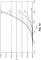
- FIG. 9 a graph showing performance transfer characteristics for the transistor is shown. As can be seen in FIG. 9 , the drain current versus gate voltage is constant at a drain voltage of 20 volts. The gate current which has very little leakage at all gate voltages is also shown. It can also be seen that the drain current responds well to the gate voltage, ranging from a small current of about 10 -11 amps at a gate of -2 volts to almost a milliamp at a gate of 10 volts. Referring to FIG.
- FIG. 10 a graph showing performance I d -V d curve characteristics for the transistor is shown. As can be seen in FIG. 10 , the drain current versus drain voltage is very responsive to the gate voltage. Test results of the devices also show a respectable on/off of greater than 10 7 for a drain voltage of 20 V and gate voltage of 10V.
Landscapes
- Thin Film Transistor (AREA)
- Internal Circuitry In Semiconductor Integrated Circuit Devices (AREA)
Applications Claiming Priority (2)
| Application Number | Priority Date | Filing Date | Title |
|---|---|---|---|
| US12/713,264 US8803203B2 (en) | 2010-02-26 | 2010-02-26 | Transistor including reentrant profile |
| PCT/US2011/024310 WO2011106165A1 (en) | 2010-02-26 | 2011-02-10 | Vertical transistor including reentrant profile |
Publications (2)
| Publication Number | Publication Date |
|---|---|
| EP2539924A1 EP2539924A1 (en) | 2013-01-02 |
| EP2539924B1 true EP2539924B1 (en) | 2019-12-11 |
Family
ID=43875263
Family Applications (1)
| Application Number | Title | Priority Date | Filing Date |
|---|---|---|---|
| EP11704703.5A Active EP2539924B1 (en) | 2010-02-26 | 2011-02-10 | Vertical transistor including reentrant profile |
Country Status (7)
| Country | Link |
|---|---|
| US (2) | US8803203B2 (enExample) |
| EP (1) | EP2539924B1 (enExample) |
| JP (1) | JP2013520839A (enExample) |
| KR (1) | KR20120114372A (enExample) |
| CN (1) | CN102782821B (enExample) |
| BR (1) | BR112012019907A2 (enExample) |
| WO (1) | WO2011106165A1 (enExample) |
Families Citing this family (10)
| Publication number | Priority date | Publication date | Assignee | Title |
|---|---|---|---|---|
| US8492769B2 (en) * | 2011-01-07 | 2013-07-23 | Eastman Kodak Company | Transistor including multi-layer reentrant profile |
| WO2012094357A2 (en) * | 2011-01-07 | 2012-07-12 | Eastman Kodak Company | Transistor including multiple reentrant profiles |
| US8962989B2 (en) | 2011-02-03 | 2015-02-24 | Solar Junction Corporation | Flexible hermetic semiconductor solar cell package with non-hermetic option |
| US8273654B1 (en) * | 2011-09-29 | 2012-09-25 | Eastman Kodak Company | Producing a vertical transistor including reentrant profile |
| US9006736B2 (en) * | 2013-07-12 | 2015-04-14 | Semiconductor Energy Laboratory Co., Ltd. | Semiconductor device |
| US9123815B1 (en) * | 2014-03-06 | 2015-09-01 | Eastman Kodak Company | VTFTs including offset electrodes |
| US9117914B1 (en) * | 2014-03-06 | 2015-08-25 | Eastman Kodak Company | VTFT with polymer core |
| US9147770B1 (en) * | 2014-03-06 | 2015-09-29 | Eastman Kodak Company | VTFT with extended electrode |
| US20150287831A1 (en) * | 2014-04-08 | 2015-10-08 | Semiconductor Energy Laboratory Co., Ltd. | Semiconductor device and electronic device including semiconductor device |
| US9691997B2 (en) * | 2014-06-11 | 2017-06-27 | Eastman Kodak Company | Devices having dielectric layers with thiosulfate-containing polymers |
Family Cites Families (38)
| Publication number | Priority date | Publication date | Assignee | Title |
|---|---|---|---|---|
| JPS63170971A (ja) | 1987-01-09 | 1988-07-14 | Nec Corp | 半導体装置 |
| ATE152287T1 (de) | 1987-12-02 | 1997-05-15 | Advanced Micro Devices Inc | Ein verfahren zur herstellung selbstausrichtender halbleiteranordnungen |
| JPH02140863A (ja) | 1988-11-22 | 1990-05-30 | Nec Corp | 分散型エディタにおける端末側エディタのテキスト送信方式 |
| JPH02140863U (enExample) | 1989-04-26 | 1990-11-26 | ||
| JPH05144744A (ja) | 1991-11-18 | 1993-06-11 | Nippon Telegr & Teleph Corp <Ntt> | 半導体薄膜形成方法 |
| KR970007965B1 (en) | 1994-05-12 | 1997-05-19 | Lg Semicon Co Ltd | Structure and fabrication method of tft |
| KR0132490B1 (ko) * | 1994-07-21 | 1998-04-16 | 문정환 | 박막트랜지스터 제조방법 |
| JPH08153878A (ja) * | 1994-11-29 | 1996-06-11 | Sony Corp | 薄膜トランジスタ及びその製造方法 |
| US5641694A (en) * | 1994-12-22 | 1997-06-24 | International Business Machines Corporation | Method of fabricating vertical epitaxial SOI transistor |
| KR0165398B1 (ko) * | 1995-05-26 | 1998-12-15 | 윤종용 | 버티칼 트랜지스터의 제조방법 |
| US5780911A (en) * | 1995-11-29 | 1998-07-14 | Lg Semicon Co., Ltd. | Thin film transistor and method for fabricating the same |
| GB0024294D0 (en) * | 2000-10-04 | 2000-11-15 | Univ Cambridge Tech | Solid state embossing of polymer devices |
| DE10234735A1 (de) * | 2002-07-30 | 2004-02-12 | Infineon Technologies Ag | Verfahren zum vertikalen Strukturieren von Substraten in der Halbleiterprozesstechnik mittels inkonformer Abscheidung |
| US6924517B2 (en) * | 2003-08-26 | 2005-08-02 | International Business Machines Corporation | Thin channel FET with recessed source/drains and extensions |
| FR2861501B1 (fr) * | 2003-10-22 | 2006-01-13 | Commissariat Energie Atomique | Dispositif microelectronique a effet de champ apte a former un ou plusiseurs canaux de transistors |
| JP3983222B2 (ja) | 2004-01-13 | 2007-09-26 | Necエレクトロニクス株式会社 | 半導体装置及びその製造方法 |
| US7629633B2 (en) * | 2004-05-20 | 2009-12-08 | Isaac Wing Tak Chan | Vertical thin film transistor with short-channel effect suppression |
| US6972461B1 (en) * | 2004-06-30 | 2005-12-06 | International Business Machines Corporation | Channel MOSFET with strained silicon channel on strained SiGe |
| CN100490180C (zh) * | 2004-10-04 | 2009-05-20 | 松下电器产业株式会社 | 纵向场效应晶体管及其制造方法 |
| JP2006269599A (ja) * | 2005-03-23 | 2006-10-05 | Sony Corp | パターン形成方法、有機電界効果型トランジスタの製造方法、及び、フレキシブルプリント回路板の製造方法 |
| TWI278068B (en) * | 2005-11-03 | 2007-04-01 | Nanya Technology Corp | Growth controlled vertical transistor |
| US7456429B2 (en) * | 2006-03-29 | 2008-11-25 | Eastman Kodak Company | Apparatus for atomic layer deposition |
| US7413982B2 (en) * | 2006-03-29 | 2008-08-19 | Eastman Kodak Company | Process for atomic layer deposition |
| JP2007284766A (ja) | 2006-04-19 | 2007-11-01 | Shimadzu Corp | 縦型プラズマcvd装置 |
| US7410856B2 (en) * | 2006-09-14 | 2008-08-12 | Micron Technology, Inc. | Methods of forming vertical transistors |
| JP2008091379A (ja) * | 2006-09-29 | 2008-04-17 | Sanyo Electric Co Ltd | 電界効果トランジスタ及びその製造方法 |
| JP2008103636A (ja) | 2006-10-20 | 2008-05-01 | Sumitomo Electric Ind Ltd | 縦型トランジスタ、および縦型トランジスタを作製する方法 |
| JP2008160004A (ja) * | 2006-12-26 | 2008-07-10 | Toshiba Corp | 半導体記憶装置及びその製造方法 |
| US11136667B2 (en) * | 2007-01-08 | 2021-10-05 | Eastman Kodak Company | Deposition system and method using a delivery head separated from a substrate by gas pressure |
| US7789961B2 (en) * | 2007-01-08 | 2010-09-07 | Eastman Kodak Company | Delivery device comprising gas diffuser for thin film deposition |
| JP2008277375A (ja) | 2007-04-26 | 2008-11-13 | Sanyo Electric Co Ltd | 電界効果トランジスタ及びその製造方法 |
| US20090001470A1 (en) * | 2007-06-26 | 2009-01-01 | Anderson Brent A | Method for forming acute-angle spacer for non-orthogonal finfet and the resulting structure |
| KR100896631B1 (ko) | 2007-08-13 | 2009-05-08 | 성균관대학교산학협력단 | 수직 실린더형 트랜지스터의 제조방법 및 이에 의해 제조된수직 실린더형 트랜지스터 |
| KR100889607B1 (ko) | 2007-08-13 | 2009-03-20 | 성균관대학교산학협력단 | 더미 드레인층을 이용한 수직 실린더형 트랜지스터의제조방법 및 이에 의해 제조된 수직 실린더형 트랜지스터 |
| JP2009130165A (ja) * | 2007-11-26 | 2009-06-11 | Sanyo Electric Co Ltd | Cmos半導体装置 |
| KR100960928B1 (ko) * | 2008-01-02 | 2010-06-07 | 주식회사 하이닉스반도체 | 수직형 트랜지스터 및 그의 형성방법 |
| JP2010040580A (ja) | 2008-07-31 | 2010-02-18 | Sanyo Electric Co Ltd | 有機薄膜デバイスの製造方法及び有機薄膜デバイス |
| US8637355B2 (en) * | 2011-08-26 | 2014-01-28 | Eastman Kodak Company | Actuating transistor including single layer reentrant profile |
-
2010
- 2010-02-26 US US12/713,264 patent/US8803203B2/en active Active
-
2011
- 2011-02-10 JP JP2012555025A patent/JP2013520839A/ja active Pending
- 2011-02-10 BR BR112012019907A patent/BR112012019907A2/pt not_active IP Right Cessation
- 2011-02-10 KR KR1020127022265A patent/KR20120114372A/ko not_active Withdrawn
- 2011-02-10 EP EP11704703.5A patent/EP2539924B1/en active Active
- 2011-02-10 WO PCT/US2011/024310 patent/WO2011106165A1/en not_active Ceased
- 2011-02-10 CN CN201180010647.7A patent/CN102782821B/zh not_active Expired - Fee Related
-
2014
- 2014-05-29 US US14/289,678 patent/US9337828B2/en not_active Expired - Fee Related
Non-Patent Citations (1)
| Title |
|---|
| None * |
Also Published As
| Publication number | Publication date |
|---|---|
| JP2013520839A (ja) | 2013-06-06 |
| US8803203B2 (en) | 2014-08-12 |
| WO2011106165A1 (en) | 2011-09-01 |
| US9337828B2 (en) | 2016-05-10 |
| CN102782821B (zh) | 2016-01-13 |
| KR20120114372A (ko) | 2012-10-16 |
| US20110210783A1 (en) | 2011-09-01 |
| EP2539924A1 (en) | 2013-01-02 |
| CN102782821A (zh) | 2012-11-14 |
| BR112012019907A2 (pt) | 2016-05-10 |
| US20140266402A1 (en) | 2014-09-18 |
Similar Documents
| Publication | Publication Date | Title |
|---|---|---|
| US7923313B1 (en) | Method of making transistor including reentrant profile | |
| EP2539924B1 (en) | Vertical transistor including reentrant profile | |
| US7985684B1 (en) | Actuating transistor including reduced channel length | |
| US8865576B2 (en) | Producing vertical transistor having reduced parasitic capacitance | |
| US8617942B2 (en) | Producing transistor including single layer reentrant profile | |
| US8803227B2 (en) | Vertical transistor having reduced parasitic capacitance | |
| US8409937B2 (en) | Producing transistor including multi-layer reentrant profile | |
| US8946070B2 (en) | Four terminal transistor fabrication | |
| US8383469B2 (en) | Producing transistor including reduced channel length | |
| US20140374762A1 (en) | Circuit including four terminal transistor | |
| US20140374806A1 (en) | Four terminal transistor | |
| EP2661774B1 (en) | Transistor including multi-layer reentrant profile | |
| US8674748B2 (en) | Actuating transistor including multi-layer reentrant profile | |
| US8637355B2 (en) | Actuating transistor including single layer reentrant profile | |
| WO2012094357A2 (en) | Transistor including multiple reentrant profiles | |
| US8338291B2 (en) | Producing transistor including multiple reentrant profiles | |
| US8592909B2 (en) | Transistor including single layer reentrant profile | |
| US8847232B2 (en) | Transistor including reduced channel length | |
| US8304347B2 (en) | Actuating transistor including multiple reentrant profiles | |
| US8847226B2 (en) | Transistor including multiple reentrant profiles | |
| WO2012094109A1 (en) | Transistor including reduced channel length |
Legal Events
| Date | Code | Title | Description |
|---|---|---|---|
| PUAI | Public reference made under article 153(3) epc to a published international application that has entered the european phase |
Free format text: ORIGINAL CODE: 0009012 |
|
| 17P | Request for examination filed |
Effective date: 20120808 |
|
| AK | Designated contracting states |
Kind code of ref document: A1 Designated state(s): AL AT BE BG CH CY CZ DE DK EE ES FI FR GB GR HR HU IE IS IT LI LT LU LV MC MK MT NL NO PL PT RO RS SE SI SK SM TR |
|
| DAX | Request for extension of the european patent (deleted) | ||
| STAA | Information on the status of an ep patent application or granted ep patent |
Free format text: STATUS: EXAMINATION IS IN PROGRESS |
|
| 17Q | First examination report despatched |
Effective date: 20180612 |
|
| GRAP | Despatch of communication of intention to grant a patent |
Free format text: ORIGINAL CODE: EPIDOSNIGR1 |
|
| STAA | Information on the status of an ep patent application or granted ep patent |
Free format text: STATUS: GRANT OF PATENT IS INTENDED |
|
| INTG | Intention to grant announced |
Effective date: 20190731 |
|
| RIN1 | Information on inventor provided before grant (corrected) |
Inventor name: TUTT, LEE WILLIAM Inventor name: NELSON, SHELBY FORRESTER |
|
| GRAS | Grant fee paid |
Free format text: ORIGINAL CODE: EPIDOSNIGR3 |
|
| GRAA | (expected) grant |
Free format text: ORIGINAL CODE: 0009210 |
|
| STAA | Information on the status of an ep patent application or granted ep patent |
Free format text: STATUS: THE PATENT HAS BEEN GRANTED |
|
| AK | Designated contracting states |
Kind code of ref document: B1 Designated state(s): AL AT BE BG CH CY CZ DE DK EE ES FI FR GB GR HR HU IE IS IT LI LT LU LV MC MK MT NL NO PL PT RO RS SE SI SK SM TR |
|
| REG | Reference to a national code |
Ref country code: GB Ref legal event code: FG4D |
|
| REG | Reference to a national code |
Ref country code: CH Ref legal event code: EP |
|
| REG | Reference to a national code |
Ref country code: AT Ref legal event code: REF Ref document number: 1213037 Country of ref document: AT Kind code of ref document: T Effective date: 20191215 |
|
| REG | Reference to a national code |
Ref country code: DE Ref legal event code: R096 Ref document number: 602011063921 Country of ref document: DE |
|
| REG | Reference to a national code |
Ref country code: IE Ref legal event code: FG4D |
|
| REG | Reference to a national code |
Ref country code: NL Ref legal event code: FP |
|
| REG | Reference to a national code |
Ref country code: LT Ref legal event code: MG4D |
|
| PG25 | Lapsed in a contracting state [announced via postgrant information from national office to epo] |
Ref country code: FI Free format text: LAPSE BECAUSE OF FAILURE TO SUBMIT A TRANSLATION OF THE DESCRIPTION OR TO PAY THE FEE WITHIN THE PRESCRIBED TIME-LIMIT Effective date: 20191211 Ref country code: BG Free format text: LAPSE BECAUSE OF FAILURE TO SUBMIT A TRANSLATION OF THE DESCRIPTION OR TO PAY THE FEE WITHIN THE PRESCRIBED TIME-LIMIT Effective date: 20200311 Ref country code: NO Free format text: LAPSE BECAUSE OF FAILURE TO SUBMIT A TRANSLATION OF THE DESCRIPTION OR TO PAY THE FEE WITHIN THE PRESCRIBED TIME-LIMIT Effective date: 20200311 Ref country code: GR Free format text: LAPSE BECAUSE OF FAILURE TO SUBMIT A TRANSLATION OF THE DESCRIPTION OR TO PAY THE FEE WITHIN THE PRESCRIBED TIME-LIMIT Effective date: 20200312 Ref country code: SE Free format text: LAPSE BECAUSE OF FAILURE TO SUBMIT A TRANSLATION OF THE DESCRIPTION OR TO PAY THE FEE WITHIN THE PRESCRIBED TIME-LIMIT Effective date: 20191211 Ref country code: LV Free format text: LAPSE BECAUSE OF FAILURE TO SUBMIT A TRANSLATION OF THE DESCRIPTION OR TO PAY THE FEE WITHIN THE PRESCRIBED TIME-LIMIT Effective date: 20191211 Ref country code: ES Free format text: LAPSE BECAUSE OF FAILURE TO SUBMIT A TRANSLATION OF THE DESCRIPTION OR TO PAY THE FEE WITHIN THE PRESCRIBED TIME-LIMIT Effective date: 20191211 Ref country code: LT Free format text: LAPSE BECAUSE OF FAILURE TO SUBMIT A TRANSLATION OF THE DESCRIPTION OR TO PAY THE FEE WITHIN THE PRESCRIBED TIME-LIMIT Effective date: 20191211 |
|
| PG25 | Lapsed in a contracting state [announced via postgrant information from national office to epo] |
Ref country code: HR Free format text: LAPSE BECAUSE OF FAILURE TO SUBMIT A TRANSLATION OF THE DESCRIPTION OR TO PAY THE FEE WITHIN THE PRESCRIBED TIME-LIMIT Effective date: 20191211 Ref country code: RS Free format text: LAPSE BECAUSE OF FAILURE TO SUBMIT A TRANSLATION OF THE DESCRIPTION OR TO PAY THE FEE WITHIN THE PRESCRIBED TIME-LIMIT Effective date: 20191211 |
|
| PG25 | Lapsed in a contracting state [announced via postgrant information from national office to epo] |
Ref country code: AL Free format text: LAPSE BECAUSE OF FAILURE TO SUBMIT A TRANSLATION OF THE DESCRIPTION OR TO PAY THE FEE WITHIN THE PRESCRIBED TIME-LIMIT Effective date: 20191211 |
|
| PG25 | Lapsed in a contracting state [announced via postgrant information from national office to epo] |
Ref country code: EE Free format text: LAPSE BECAUSE OF FAILURE TO SUBMIT A TRANSLATION OF THE DESCRIPTION OR TO PAY THE FEE WITHIN THE PRESCRIBED TIME-LIMIT Effective date: 20191211 Ref country code: RO Free format text: LAPSE BECAUSE OF FAILURE TO SUBMIT A TRANSLATION OF THE DESCRIPTION OR TO PAY THE FEE WITHIN THE PRESCRIBED TIME-LIMIT Effective date: 20191211 Ref country code: CZ Free format text: LAPSE BECAUSE OF FAILURE TO SUBMIT A TRANSLATION OF THE DESCRIPTION OR TO PAY THE FEE WITHIN THE PRESCRIBED TIME-LIMIT Effective date: 20191211 Ref country code: PT Free format text: LAPSE BECAUSE OF FAILURE TO SUBMIT A TRANSLATION OF THE DESCRIPTION OR TO PAY THE FEE WITHIN THE PRESCRIBED TIME-LIMIT Effective date: 20200506 |
|
| PG25 | Lapsed in a contracting state [announced via postgrant information from national office to epo] |
Ref country code: SM Free format text: LAPSE BECAUSE OF FAILURE TO SUBMIT A TRANSLATION OF THE DESCRIPTION OR TO PAY THE FEE WITHIN THE PRESCRIBED TIME-LIMIT Effective date: 20191211 Ref country code: SK Free format text: LAPSE BECAUSE OF FAILURE TO SUBMIT A TRANSLATION OF THE DESCRIPTION OR TO PAY THE FEE WITHIN THE PRESCRIBED TIME-LIMIT Effective date: 20191211 Ref country code: IS Free format text: LAPSE BECAUSE OF FAILURE TO SUBMIT A TRANSLATION OF THE DESCRIPTION OR TO PAY THE FEE WITHIN THE PRESCRIBED TIME-LIMIT Effective date: 20200411 |
|
| REG | Reference to a national code |
Ref country code: DE Ref legal event code: R097 Ref document number: 602011063921 Country of ref document: DE |
|
| REG | Reference to a national code |
Ref country code: CH Ref legal event code: PL |
|
| REG | Reference to a national code |
Ref country code: AT Ref legal event code: MK05 Ref document number: 1213037 Country of ref document: AT Kind code of ref document: T Effective date: 20191211 |
|
| PLBE | No opposition filed within time limit |
Free format text: ORIGINAL CODE: 0009261 |
|
| STAA | Information on the status of an ep patent application or granted ep patent |
Free format text: STATUS: NO OPPOSITION FILED WITHIN TIME LIMIT |
|
| REG | Reference to a national code |
Ref country code: BE Ref legal event code: MM Effective date: 20200229 |
|
| PG25 | Lapsed in a contracting state [announced via postgrant information from national office to epo] |
Ref country code: DK Free format text: LAPSE BECAUSE OF FAILURE TO SUBMIT A TRANSLATION OF THE DESCRIPTION OR TO PAY THE FEE WITHIN THE PRESCRIBED TIME-LIMIT Effective date: 20191211 Ref country code: MC Free format text: LAPSE BECAUSE OF FAILURE TO SUBMIT A TRANSLATION OF THE DESCRIPTION OR TO PAY THE FEE WITHIN THE PRESCRIBED TIME-LIMIT Effective date: 20191211 Ref country code: LU Free format text: LAPSE BECAUSE OF NON-PAYMENT OF DUE FEES Effective date: 20200210 |
|
| 26N | No opposition filed |
Effective date: 20200914 |
|
| PG25 | Lapsed in a contracting state [announced via postgrant information from national office to epo] |
Ref country code: PL Free format text: LAPSE BECAUSE OF FAILURE TO SUBMIT A TRANSLATION OF THE DESCRIPTION OR TO PAY THE FEE WITHIN THE PRESCRIBED TIME-LIMIT Effective date: 20191211 Ref country code: AT Free format text: LAPSE BECAUSE OF FAILURE TO SUBMIT A TRANSLATION OF THE DESCRIPTION OR TO PAY THE FEE WITHIN THE PRESCRIBED TIME-LIMIT Effective date: 20191211 Ref country code: CH Free format text: LAPSE BECAUSE OF NON-PAYMENT OF DUE FEES Effective date: 20200229 Ref country code: LI Free format text: LAPSE BECAUSE OF NON-PAYMENT OF DUE FEES Effective date: 20200229 Ref country code: SI Free format text: LAPSE BECAUSE OF FAILURE TO SUBMIT A TRANSLATION OF THE DESCRIPTION OR TO PAY THE FEE WITHIN THE PRESCRIBED TIME-LIMIT Effective date: 20191211 |
|
| PG25 | Lapsed in a contracting state [announced via postgrant information from national office to epo] |
Ref country code: FR Free format text: LAPSE BECAUSE OF NON-PAYMENT OF DUE FEES Effective date: 20200211 Ref country code: IE Free format text: LAPSE BECAUSE OF NON-PAYMENT OF DUE FEES Effective date: 20200210 Ref country code: IT Free format text: LAPSE BECAUSE OF FAILURE TO SUBMIT A TRANSLATION OF THE DESCRIPTION OR TO PAY THE FEE WITHIN THE PRESCRIBED TIME-LIMIT Effective date: 20191211 |
|
| PG25 | Lapsed in a contracting state [announced via postgrant information from national office to epo] |
Ref country code: BE Free format text: LAPSE BECAUSE OF NON-PAYMENT OF DUE FEES Effective date: 20200229 |
|
| PGFP | Annual fee paid to national office [announced via postgrant information from national office to epo] |
Ref country code: GB Payment date: 20220125 Year of fee payment: 12 Ref country code: DE Payment date: 20220112 Year of fee payment: 12 |
|
| PG25 | Lapsed in a contracting state [announced via postgrant information from national office to epo] |
Ref country code: TR Free format text: LAPSE BECAUSE OF FAILURE TO SUBMIT A TRANSLATION OF THE DESCRIPTION OR TO PAY THE FEE WITHIN THE PRESCRIBED TIME-LIMIT Effective date: 20191211 Ref country code: MT Free format text: LAPSE BECAUSE OF FAILURE TO SUBMIT A TRANSLATION OF THE DESCRIPTION OR TO PAY THE FEE WITHIN THE PRESCRIBED TIME-LIMIT Effective date: 20191211 Ref country code: CY Free format text: LAPSE BECAUSE OF FAILURE TO SUBMIT A TRANSLATION OF THE DESCRIPTION OR TO PAY THE FEE WITHIN THE PRESCRIBED TIME-LIMIT Effective date: 20191211 |
|
| PGFP | Annual fee paid to national office [announced via postgrant information from national office to epo] |
Ref country code: NL Payment date: 20220114 Year of fee payment: 12 |
|
| PG25 | Lapsed in a contracting state [announced via postgrant information from national office to epo] |
Ref country code: MK Free format text: LAPSE BECAUSE OF FAILURE TO SUBMIT A TRANSLATION OF THE DESCRIPTION OR TO PAY THE FEE WITHIN THE PRESCRIBED TIME-LIMIT Effective date: 20191211 |
|
| REG | Reference to a national code |
Ref country code: DE Ref legal event code: R119 Ref document number: 602011063921 Country of ref document: DE |
|
| REG | Reference to a national code |
Ref country code: NL Ref legal event code: MM Effective date: 20230301 |
|
| GBPC | Gb: european patent ceased through non-payment of renewal fee |
Effective date: 20230210 |
|
| PG25 | Lapsed in a contracting state [announced via postgrant information from national office to epo] |
Ref country code: NL Free format text: LAPSE BECAUSE OF NON-PAYMENT OF DUE FEES Effective date: 20230301 |
|
| PG25 | Lapsed in a contracting state [announced via postgrant information from national office to epo] |
Ref country code: GB Free format text: LAPSE BECAUSE OF NON-PAYMENT OF DUE FEES Effective date: 20230210 |
|
| PG25 | Lapsed in a contracting state [announced via postgrant information from national office to epo] |
Ref country code: GB Free format text: LAPSE BECAUSE OF NON-PAYMENT OF DUE FEES Effective date: 20230210 Ref country code: DE Free format text: LAPSE BECAUSE OF NON-PAYMENT OF DUE FEES Effective date: 20230901 |