EP2537183B1 - Structure de blindage pour lignes de transmission - Google Patents
Structure de blindage pour lignes de transmission Download PDFInfo
- Publication number
- EP2537183B1 EP2537183B1 EP11745210.2A EP11745210A EP2537183B1 EP 2537183 B1 EP2537183 B1 EP 2537183B1 EP 11745210 A EP11745210 A EP 11745210A EP 2537183 B1 EP2537183 B1 EP 2537183B1
- Authority
- EP
- European Patent Office
- Prior art keywords
- comb
- metallization layer
- vias
- array
- structures
- Prior art date
- Legal status (The legal status is an assumption and is not a legal conclusion. Google has not performed a legal analysis and makes no representation as to the accuracy of the status listed.)
- Active
Links
- 230000005540 biological transmission Effects 0.000 title description 10
- 238000001465 metallisation Methods 0.000 claims description 63
- 238000003491 array Methods 0.000 claims description 12
- 239000000758 substrate Substances 0.000 description 7
- 238000000034 method Methods 0.000 description 5
- 239000004065 semiconductor Substances 0.000 description 5
- 238000005516 engineering process Methods 0.000 description 3
- XUIMIQQOPSSXEZ-UHFFFAOYSA-N Silicon Chemical compound [Si] XUIMIQQOPSSXEZ-UHFFFAOYSA-N 0.000 description 2
- 238000003780 insertion Methods 0.000 description 2
- 230000037431 insertion Effects 0.000 description 2
- 229910052751 metal Inorganic materials 0.000 description 2
- 239000002184 metal Substances 0.000 description 2
- 229910052710 silicon Inorganic materials 0.000 description 2
- 239000010703 silicon Substances 0.000 description 2
- RYGMFSIKBFXOCR-UHFFFAOYSA-N Copper Chemical compound [Cu] RYGMFSIKBFXOCR-UHFFFAOYSA-N 0.000 description 1
- 239000004411 aluminium Substances 0.000 description 1
- 229910052782 aluminium Inorganic materials 0.000 description 1
- XAGFODPZIPBFFR-UHFFFAOYSA-N aluminium Chemical compound [Al] XAGFODPZIPBFFR-UHFFFAOYSA-N 0.000 description 1
- 230000015572 biosynthetic process Effects 0.000 description 1
- 239000004020 conductor Substances 0.000 description 1
- 229910052802 copper Inorganic materials 0.000 description 1
- 239000010949 copper Substances 0.000 description 1
- 230000008878 coupling Effects 0.000 description 1
- 238000010168 coupling process Methods 0.000 description 1
- 238000005859 coupling reaction Methods 0.000 description 1
- 238000005530 etching Methods 0.000 description 1
- 238000004519 manufacturing process Methods 0.000 description 1
- 230000004048 modification Effects 0.000 description 1
- 238000012986 modification Methods 0.000 description 1
- 230000003071 parasitic effect Effects 0.000 description 1
- 230000011664 signaling Effects 0.000 description 1
Images


Classifications
-
- H—ELECTRICITY
- H01—ELECTRIC ELEMENTS
- H01L—SEMICONDUCTOR DEVICES NOT COVERED BY CLASS H10
- H01L29/00—Semiconductor devices specially adapted for rectifying, amplifying, oscillating or switching and having potential barriers; Capacitors or resistors having potential barriers, e.g. a PN-junction depletion layer or carrier concentration layer; Details of semiconductor bodies or of electrodes thereof ; Multistep manufacturing processes therefor
- H01L29/66—Types of semiconductor device ; Multistep manufacturing processes therefor
- H01L29/86—Types of semiconductor device ; Multistep manufacturing processes therefor controllable only by variation of the electric current supplied, or only the electric potential applied, to one or more of the electrodes carrying the current to be rectified, amplified, oscillated or switched
- H01L29/92—Capacitors having potential barriers
-
- H—ELECTRICITY
- H01—ELECTRIC ELEMENTS
- H01L—SEMICONDUCTOR DEVICES NOT COVERED BY CLASS H10
- H01L23/00—Details of semiconductor or other solid state devices
- H01L23/52—Arrangements for conducting electric current within the device in operation from one component to another, i.e. interconnections, e.g. wires, lead frames
- H01L23/522—Arrangements for conducting electric current within the device in operation from one component to another, i.e. interconnections, e.g. wires, lead frames including external interconnections consisting of a multilayer structure of conductive and insulating layers inseparably formed on the semiconductor body
- H01L23/5222—Capacitive arrangements or effects of, or between wiring layers
- H01L23/5225—Shielding layers formed together with wiring layers
-
- H—ELECTRICITY
- H01—ELECTRIC ELEMENTS
- H01L—SEMICONDUCTOR DEVICES NOT COVERED BY CLASS H10
- H01L23/00—Details of semiconductor or other solid state devices
- H01L23/552—Protection against radiation, e.g. light or electromagnetic waves
-
- H—ELECTRICITY
- H01—ELECTRIC ELEMENTS
- H01L—SEMICONDUCTOR DEVICES NOT COVERED BY CLASS H10
- H01L2924/00—Indexing scheme for arrangements or methods for connecting or disconnecting semiconductor or solid-state bodies as covered by H01L24/00
- H01L2924/0001—Technical content checked by a classifier
- H01L2924/0002—Not covered by any one of groups H01L24/00, H01L24/00 and H01L2224/00
Definitions
- This relates to shielding structures formed in the back end of integrated circuits.
- a typical integrated circuit comprises a semiconductor substrate in and on which are defined a multitude of transistors and a series of metal interconnect layers on top of the substrate.
- the interconnect layers are insulated from one another by intermetallic dielectric layers.
- Interconnection paths are defined in the metallic layers and selective connections are made between the paths in the various layers so as to connect the transistors formed in the substrate to each other and to external connections.
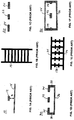
- FIGS. 1A -1F depict cross-sections of several conventional shielding structures.
- a microstrip 10 comprises a signal line 12 located above and insulated from a ground plane 14 that provides a current return path.
- a pair of transmission lines may be used in place of a single signal line to provide differential-type signaling.
- the signal line 12 is defined in one metallization layer
- the ground plane 14 is defined in a second metallization layer and the signal line and ground plane are separated by at least one intermetallic dielectric layer.
- ground plane 14 may be a continuous two-dimensional sheet with no openings in it or may comprise a plurality of metal strips connected together at each end in a ladder-like configuration as shown in the horizontal section of FIG.1B .
- Other patterns of connected metallization may also be used; and in some cases the ground plane can be the silicon substrate.
- a co-planar waveguide (CPW) 20 comprises a signal line 22 located between two ground planes 24, 25.
- the signal line and ground planes of the coplanar waveguide are all implemented in the same metallization layer and insulated from the substrate of the integrated circuit by at least one intermetallic dielectric layer.
- each ground plane may be a continuous two-dimensional sheet with no openings or it may comprise a ladder-like array of connected strips as shown in FIG. 1B . Other patterns of connected metallization may also be used.
- a grounded co-planar waveguide (GCPW) 30 comprises a signal line 32 located between two ground planes 34, 35 and above a third ground plane 36.
- the ground planes 34, 35 are electrically connected to ground plane 36 by electrically conductive sidewalls 38, 39.
- signal line 32 and ground planes 34, 35 are defined in a first metallization layer
- ground plane 36 is defined in a second metallization layer beneath the first layer
- the first and second metallization layers are separated by at least one intermetallic dielectric layer.
- ground plane 36 may be a continuous two-dimensional sheet with no openings or it may comprise a ladder-like array of connected strips as shown in FIG.
- the sidewalls are formed using stacks of vias that extend between the upper and lower metallization layers. As shown in the lateral section of FIG. 1E , a first plurality of electrically conducting via stacks 138 form a sidewall that connects upper ground plane 34 to lower ground plane 36 and a second plurality of electrically conducting via stacks similar to that of FIG. 1E forms a sidewall that connects upper ground plane 35 to lower ground plane 36. Additional rows of electrically conducting vias may be connected in parallel to connect the upper and lower ground planes.
- a stripline 50 comprises a signal line 52 located between an upper ground plane 54 and a lower ground plane 56.
- the upper and lower ground planes are electrically connected by electrically conductive sidewalls 58, 59 so that the signal line is in the center of the region enclosed by the ground planes and sidewalls.
- signal line 52 is defined in one metallization layer
- ground plane 54 is defined in a second metallization layer above it
- ground plane 56 is defmed in a third metallization layer below it.
- a first plurality of electrically conducting vias form a sidewall that connects upper ground plane 54 to lower ground plane 56 on one side of the signal line 52; and a second plurality of electrically conducting vias form a sidewall that connects upper ground plane 54 to lower ground plane 56 on the other side of signal line 52.
- the ground planes may be continuous two-dimensional sheets with no openings or ladder-like arrays of connected strips as shown in FIG. 1B or some other pattern of connected metallization; and the vias may be similar to those shown in FIG. 1E .
- US 2003/237070 describes a method of designing a semiconductor circuit including external wiring and shield wiring designing steps.
- US 2009/0315641 describes a structure of on-chip variable delay transmission lines with a fixed characteristic impedance.
- the present invention is an improved shielding structure that can be implemented in the metallization layers of an integrated circuit.
- the improved shielding structure reduces parasitic coupling between the transmission line(s) and the shielding structure with the result that the shielding structure has lower insertion loss than prior art shielding structures. Further, it has a better signal/noise ratio.
- At least one signal line is located in the second metallization layer between the first and second planar structures; and the first and second comb-like structures, the first and second planar structures and the first, second, third, and fourth electrically conducting vias are all at substantially the same potential, which preferably is ground.
- a pair of signal lines may be used to carry differential-type signals; the first and second planar structures may also be comb-like structures; and multiple rows of electrically conducting vias may extend from the planar structures and/or the comb-like structures.
- the preferred embodiment may be regarded as a modification of a grounded co-planar waveguide, the invention may also be practiced in other types of waveguides such as microstrips and striplines.
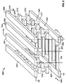
- FIG. 2 is a perspective view of an illustrative example of a shielding structure 200 of the present invention
- FIGS. 3 and 4 are cross-sections along lines 3-3 and 4-4, respectively, of FIG. 2
- Shielding structure 200 is formed in an integrated circuit in a plurality of metallization layers 211 - 214 on a semiconductor substrate 220.
- the metallization layers are separated from each other and from substrate 220 by intermetallic dielectric layers 231 - 234 (shown in FIG. 4 but now shown in FIG. 2 for reasons of clarity).
- Shielding structure 200 comprises first and second comb-like structures 240 245 defined in first metallization layer 211, each comb-like structure comprising first and second pluralities of teeth 242, 247 that extend toward the other comb-like structure; a first plurality of electrically conducting vias 250 that extend upward from the first comb-like structure 240; a second plurality of electrically conducting vias 255 that extend upward from the second comb-like structure 245; first and second planar structures 260, 265 in a second metallization layer 214 above the first metallization layer; a third plurality of electrically conducting vias 270 that extend downward from the first planar structure 260 toward the first plurality of electrically conducting vias 250; and a fourth plurality of electrically conducting vias 275 that extend downward from the second planar structure 265 toward the second plurality of electrically conducting vias, 255.
- Signal lines 280, 282 are located in metallization layer 214 between the first and second planar structures.
- the first and second comb-like structures, the first and second planar structures, and the first, second, third and fourth electrically conducting vias are all at the same potential, preferably ground.
- the metallization layers are the uppermost metallization layers of an integrated circuit.
- metallization layer 214 might be the uppermost layer of the integrated circuit while metallization layer 211 might be several layers below it, the number of layers depending on various design criteria. In other cases, metallization layer 214 might not be the uppermost layer of the integrated circuit.
- FIG. 3 A horizontal cross-section of metallization layer 211 along line 3 - 3 of FIG. 2 is shown in FIG. 3 .
- the first comb-like structure 240 comprises a first plurality of teeth 242; and the second comb-like structure 245 comprises a second plurality of teeth 247.
- the teeth are parallel to one another.
- the teeth of the first plurality are connected together by a first transverse element 244; and the teeth of the second plurality are connected together by a second transverse element 249.
- the teeth of the first comb-like structure 240 extend between the teeth of the second comb-like structure 240 but they do not contact the teeth of the second comb-like structure. However, as indicated above, the teeth are at the same potential. To accomplish this, an electrical connection is maintained between the two comb-like structures if only through the ground connection. Alternatively, one or a small number ( ⁇ 10%) of the teeth of the two comb-like structures may be directly connected together (not shown).
- the comb-like structures 240, 245 are formed by defining the structures in metallization layer 211 using well-known etching technology to define the appropriate patterns in the metallization layer...
- FIG. 4 A vertical cross-section through vias 250, 270 along line 4 - 4 of FIG. 2 is shown in FIG. 4 .
- the vertical cross-section through vias 255, 275 is similar.
- vias 250 extend upward in stacks 252 from metallization layer 211, through intermetallic dielectric layer 232, metallization layer 212, and intermetallic dielectric layer 233 to metallization layer 213.
- stacks 252 do not reach metallization layer 214.
- Vias 270 extend downward in stacks 272 from metallization layer 214, through intermetallic dielectric layer 234, metallization layer 213, and intermetallic dielectric layer 233 to metallization layer 212.
- stacks 272 do not reach metallization layer 211.
- vias 250 and vias 270 are at the same potential. To accomplish this, some of vias 250, 270 may be connected to each other by extending the via stack to the appropriate metallization layer or by connecting the stacks by metallization layers 212 and/or 213. Only a small number ⁇ 10%) of vias relative to the total number of vias should be connected in this way. Alternatively, the vias may be connected together through the ground connection.
- the vias are formed by conventional semiconductor processes in which holes are etched in an intermetallic dielectric layer down to the metallic layer immediately below and the holes are then filled with a conducting material such as aluminium or copper. Well known processes are then used to form the next metallic layer on top of the dielectric layer so that it is electrically connected to the filled holes; and this layer is then etched to separate the via stacks. A dielectric layer is then formed on the metallic layer; and the process is repeated to form the next layer of vias in the stacks. Further details on the via formation process may be found at pages 702-706 of Plummer, cited above, which are hereby incorporated by reference herein.
- the first and second planar structures may be comb-like structures; and multiple rows of electrically conducting vias may extend from the planar structures and/or the comb-like structures.
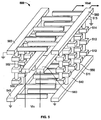
- a stripline can be implemented in which first and second comb-like structures 540, 545 are defined in a lower metallization layer 511, third and fourth comb-like structures 560, 565 are defined in an upper metallization layer 515; and one or more signal lines 580, 582 are defined in a third metallization layer 513 located between the upper and lower metallization layers.
- first and second comb-like structures 540, 545 are defined in a lower metallization layer 511
- third and fourth comb-like structures 560, 565 are defined in an upper metallization layer 515
- one or more signal lines 580, 582 are defined in a third metallization layer 513 located between the upper and lower metallization layers.
- horizontal sections through both the lower metallization layer and the upper metallization layer are the same as that depicted in FIG. 3 .
- the stripline 4 may be formed by extending via stacks upwards from the comb-like structures in the lower metallization layer and downwards from the comb-like structures in the upper metallization layer.
- the stripline is formed in five metallization layers 511 - 515; but the invention may be practiced using a greater number or a lesser number of metallization layers.
- FIG. 6 A plot of simulated transmission loss versus frequency is set forth in FIG. 6 . As shown therein, at 12.5 GHz the transmission loss for the waveguide of FIG. 2 is 10.1 dB/mm while the loss for the conventional waveguide is 12.6 dB/mm.
- FIG. 3 depicts an arrangement in which each finger of comb-like structure 240 extends between two fingers of comb-like structure 24
- comb-like structures could be used where a pair of fingers 742 of one comb-like structure 740 extend between two pairs of fingers 747 of the second comb-like structure 745, as depicted in FIG. 7 or where a triplet of fingers 842 of one comb-like structure 840 extend between two triplets of fingers 847 of the second comb-like structure 845 as depicted in FIG. 8 .
- FIGS. 2 and 5 disclose structures in which the transmission lines are formed in the same metallization layer, structures may also be used in which the transmission lines are located in different metallization layers.
Landscapes
- Power Engineering (AREA)
- Engineering & Computer Science (AREA)
- Microelectronics & Electronic Packaging (AREA)
- Physics & Mathematics (AREA)
- Computer Hardware Design (AREA)
- Condensed Matter Physics & Semiconductors (AREA)
- General Physics & Mathematics (AREA)
- Health & Medical Sciences (AREA)
- Ceramic Engineering (AREA)
- Toxicology (AREA)
- Electromagnetism (AREA)
- Internal Circuitry In Semiconductor Integrated Circuit Devices (AREA)
- Semiconductor Integrated Circuits (AREA)
- Design And Manufacture Of Integrated Circuits (AREA)
Claims (9)
- Structure de blindage comprenant :des premier et deuxième réseaux (540, 545) d'éléments conducteurs définis dans une première couche de métallisation (511) sur un circuit intégré, les éléments conducteurs du premier réseau étant reliés entre eux et s'étendant entre les éléments conducteurs du deuxième réseau, les éléments conducteurs du deuxième réseau étant reliés entre eux ;des troisième et quatrième réseaux (560, 565) d'éléments conducteurs définis dans une deuxième couche de métallisation (515) sur le circuit intégré, les éléments conducteurs du troisième réseau étant reliés entre eux et s'étendant entre les éléments conducteurs du quatrième réseau, les éléments conducteurs du quatrième réseau étant reliés entre eux ; etau moins une ligne de signal (580) dans une troisième couche de métallisation (513) entre les premier et deuxième réseaux d'éléments conducteurs dans la première couche de métallisation et les troisième et quatrième réseaux d'éléments conducteurs dans la deuxième couche de métallisation ; etles premier, deuxième, troisième et quatrième réseaux d'éléments conducteurs étant tous au même potentiel.
- Structure de blindage de la revendication 1, dans laquelle au moins l'un des premier et deuxième réseaux est une structure en forme de peigne.
- Structure de blindage de la revendication 1, dans laquelle les premier et deuxième réseaux sont des première et deuxième structures en forme de peigne, chaque structure en forme de peigne comprenant une pluralité de dents, les dents de la première structure en forme de peigne et les dents de la deuxième structure en forme de peigne s'étendant les unes vers les autres.
- Structure de blindage de la revendication 1, dans laquelle les troisième et quatrième réseaux sont des troisième et quatrième structures en forme de peigne, chaque structure en forme de peigne comprenant une pluralité de dents, les dents de la troisième structure en forme de peigne et les dents de la quatrième structure en forme de peigne s'étendant les unes vers les autres.
- Structure de blindage de la revendication 1, dans laquelle une deuxième ligne de signal (582) est située dans une couche de métallisation entre les premier et deuxième réseaux dans la première couche de métallisation et les troisième et quatrième réseaux dans la deuxième couche de métallisation.
- Structure de blindage de la revendication 5, dans laquelle la deuxième ligne de signal est située dans une quatrième couche de métallisation entre les première et deuxième couches de métallisation.
- Structure de blindage de la revendication 1 comprenant en outre une première pluralité de trous d'interconnexion électriquement conducteurs s'étendant entre le premier réseau et le troisième réseau et une deuxième pluralité de trous d'interconnexion électriquement conducteurs s'étendant entre le deuxième réseau et le quatrième réseau.
- Structure de blindage de la revendication 7, dans laquelle certains des trous d'interconnexion de la première pluralité de trous d'interconnexion s'étendent à partir du premier réseau vers le troisième réseau et certains des trous d'interconnexion de la première pluralité de trous d'interconnexion s'étendent à partir du troisième réseau vers le premier réseau.
- Structure de blindage de la revendication 7, dans laquelle les première et deuxième pluralités de trous d'interconnexion sont au même potentiel que les premier, deuxième, troisième et quatrième réseaux.
Applications Claiming Priority (2)
| Application Number | Priority Date | Filing Date | Title |
|---|---|---|---|
| US12/709,289 US7999361B1 (en) | 2010-02-19 | 2010-02-19 | Shielding structure for transmission lines |
| PCT/US2011/025194 WO2011103266A2 (fr) | 2010-02-19 | 2011-02-17 | Structure de blindage pour lignes de transmission |
Publications (3)
| Publication Number | Publication Date |
|---|---|
| EP2537183A2 EP2537183A2 (fr) | 2012-12-26 |
| EP2537183A4 EP2537183A4 (fr) | 2014-03-26 |
| EP2537183B1 true EP2537183B1 (fr) | 2016-04-06 |
Family
ID=44358544
Family Applications (1)
| Application Number | Title | Priority Date | Filing Date |
|---|---|---|---|
| EP11745210.2A Active EP2537183B1 (fr) | 2010-02-19 | 2011-02-17 | Structure de blindage pour lignes de transmission |
Country Status (5)
| Country | Link |
|---|---|
| US (3) | US7999361B1 (fr) |
| EP (1) | EP2537183B1 (fr) |
| JP (1) | JP5756816B2 (fr) |
| CN (1) | CN102844864B (fr) |
| WO (1) | WO2011103266A2 (fr) |
Families Citing this family (11)
| Publication number | Priority date | Publication date | Assignee | Title |
|---|---|---|---|---|
| JP5842368B2 (ja) * | 2011-04-11 | 2016-01-13 | ソニー株式会社 | 半導体装置 |
| JP2014120710A (ja) * | 2012-12-19 | 2014-06-30 | Nippon Telegr & Teleph Corp <Ntt> | 多層高周波伝送線路およびその製造方法 |
| US9245603B2 (en) * | 2013-10-21 | 2016-01-26 | Macronix International Co., Ltd. | Integrated circuit and operating method for the same |
| JP6244967B2 (ja) * | 2014-02-19 | 2017-12-13 | 株式会社ソシオネクスト | キャパシタアレイおよびad変換器 |
| JP2017034155A (ja) * | 2015-08-04 | 2017-02-09 | 大日本印刷株式会社 | 表示装置 |
| CN105762136B (zh) * | 2016-04-20 | 2018-12-14 | 佛山臻智微芯科技有限公司 | 差动传输线屏蔽结构 |
| US10939541B2 (en) * | 2017-03-31 | 2021-03-02 | Huawei Technologies Co., Ltd. | Shield structure for a low crosstalk single ended clock distribution circuit |
| US10236573B2 (en) * | 2017-06-20 | 2019-03-19 | Qualcomm Incorporated | On-chip coupling capacitor with patterned radio frequency shielding structure for lower loss |
| US10446898B2 (en) | 2017-06-29 | 2019-10-15 | Qualcomm Incorporated | On-chip coplanar waveguide having a shielding layer comprising a capacitor formed by sets of interdigitated fingers |
| JP7082019B2 (ja) * | 2018-09-18 | 2022-06-07 | 株式会社東芝 | 固体撮像装置 |
| WO2023140090A1 (fr) * | 2022-01-20 | 2023-07-27 | パナソニックIpマネジメント株式会社 | Guide d'ondes |
Family Cites Families (29)
| Publication number | Priority date | Publication date | Assignee | Title |
|---|---|---|---|---|
| US6885275B1 (en) * | 1998-11-12 | 2005-04-26 | Broadcom Corporation | Multi-track integrated spiral inductor |
| US6870456B2 (en) * | 1999-11-23 | 2005-03-22 | Intel Corporation | Integrated transformer |
| JP2002050742A (ja) * | 2000-07-31 | 2002-02-15 | Nec Corp | 半導体装置およびその製造方法 |
| JP4553461B2 (ja) * | 2000-08-23 | 2010-09-29 | ルネサスエレクトロニクス株式会社 | 半導体装置、その設計方法および設計装置 |
| US6496402B1 (en) * | 2000-10-17 | 2002-12-17 | Intel Corporation | Noise suppression for open bit line DRAM architectures |
| DE10063376A1 (de) * | 2000-12-19 | 2002-06-20 | Philips Corp Intellectual Pty | Hochdruckentladungslampe |
| US6903459B2 (en) * | 2001-05-17 | 2005-06-07 | Matsushita Electric Industrial Co., Ltd. | High frequency semiconductor device |
| US6970064B2 (en) * | 2001-09-05 | 2005-11-29 | Zhang Minghao Mary | Center-tap transformers in integrated circuits |
| JP3599017B2 (ja) * | 2001-11-20 | 2004-12-08 | 日本電気株式会社 | クロック伝搬遅延時間の調整方法 |
| US6747340B2 (en) * | 2002-03-15 | 2004-06-08 | Memx, Inc. | Multi-level shielded multi-conductor interconnect bus for MEMS |
| JP2004031389A (ja) * | 2002-06-21 | 2004-01-29 | Fujitsu Ltd | 半導体回路設計方法、半導体回路設計装置、プログラム及び半導体装置 |
| JP3906139B2 (ja) * | 2002-10-16 | 2007-04-18 | 株式会社東芝 | 磁気ランダムアクセスメモリ |
| JP2004140308A (ja) * | 2002-10-16 | 2004-05-13 | Adorinkusu:Kk | スリット法を用いた高速信号用プリント配線基板 |
| CA2418674A1 (fr) * | 2003-02-07 | 2004-08-07 | Tak Shun Cheung | Lignes de transmission et elements de ligne de transmission a reduction de longueur d'onde et blindage |
| JP4141881B2 (ja) * | 2003-04-04 | 2008-08-27 | シャープ株式会社 | 集積回路 |
| JP4619705B2 (ja) * | 2004-01-15 | 2011-01-26 | 株式会社東芝 | 半導体装置 |
| JP3793202B2 (ja) * | 2004-02-02 | 2006-07-05 | キヤノン株式会社 | 固体撮像装置 |
| US7123118B2 (en) * | 2004-03-08 | 2006-10-17 | Wemtec, Inc. | Systems and methods for blocking microwave propagation in parallel plate structures utilizing cluster vias |
| DE102004014752B4 (de) * | 2004-03-25 | 2008-11-20 | Infineon Technologies Ag | Halbleiterbauelement mit kernlosem Wandler und Halbbrücke |
| EP3358670A1 (fr) * | 2004-06-28 | 2018-08-08 | Mitsubishi Electric Corporation | Substrat diélectrique multicouche et boîtier semi-conducteur |
| JP4099672B2 (ja) * | 2004-12-21 | 2008-06-11 | セイコーエプソン株式会社 | 半導体装置 |
| US20060139117A1 (en) * | 2004-12-23 | 2006-06-29 | Brunker David L | Multi-channel waveguide structure |
| US7576382B2 (en) * | 2005-02-02 | 2009-08-18 | Ricoh Company, Ltd. | Semiconductor integrated device and method of providing shield interconnection therein |
| JP5008872B2 (ja) * | 2005-02-02 | 2012-08-22 | 株式会社リコー | 半導体集積装置 |
| JP5211694B2 (ja) * | 2006-01-04 | 2013-06-12 | 富士通株式会社 | 半導体集積回路におけるシールド線の配置方法、半導体集積回路の設計装置、及び半導体集積回路の設計プログラム |
| US7755457B2 (en) * | 2006-02-07 | 2010-07-13 | Harris Corporation | Stacked stripline circuits |
| JP2007306290A (ja) * | 2006-05-11 | 2007-11-22 | Univ Of Tokyo | 伝送線路 |
| US8193878B2 (en) | 2008-06-24 | 2012-06-05 | International Business Machines Corporation | Structure, structure and method for providing an on-chip variable delay transmission line with fixed characteristic impedance |
| US8022784B2 (en) * | 2008-07-07 | 2011-09-20 | Korea Advanced Institute Of Science And Technology (Kaist) | Planar transmission line-to-waveguide transition apparatus having an embedded bent stub |
-
2010
- 2010-02-19 US US12/709,289 patent/US7999361B1/en active Active
-
2011
- 2011-02-17 WO PCT/US2011/025194 patent/WO2011103266A2/fr active Application Filing
- 2011-02-17 JP JP2012554018A patent/JP5756816B2/ja not_active Expired - Fee Related
- 2011-02-17 EP EP11745210.2A patent/EP2537183B1/fr active Active
- 2011-02-17 CN CN201180018461.6A patent/CN102844864B/zh active Active
- 2011-08-09 US US13/206,169 patent/US8558355B2/en active Active
-
2013
- 2013-09-27 US US14/040,300 patent/US8823135B2/en active Active
Also Published As
| Publication number | Publication date |
|---|---|
| WO2011103266A3 (fr) | 2011-11-24 |
| CN102844864B (zh) | 2015-08-26 |
| EP2537183A2 (fr) | 2012-12-26 |
| US7999361B1 (en) | 2011-08-16 |
| CN102844864A (zh) | 2012-12-26 |
| US20110291248A1 (en) | 2011-12-01 |
| JP5756816B2 (ja) | 2015-07-29 |
| EP2537183A4 (fr) | 2014-03-26 |
| US8558355B2 (en) | 2013-10-15 |
| US20110204493A1 (en) | 2011-08-25 |
| JP2013520797A (ja) | 2013-06-06 |
| US20140048915A1 (en) | 2014-02-20 |
| WO2011103266A2 (fr) | 2011-08-25 |
| US8823135B2 (en) | 2014-09-02 |
Similar Documents
| Publication | Publication Date | Title |
|---|---|---|
| EP2537183B1 (fr) | Structure de blindage pour lignes de transmission | |
| US8324979B2 (en) | Coupled microstrip lines with ground planes having ground strip shields and ground conductor extensions | |
| US8841771B2 (en) | Semiconductor device | |
| KR100939648B1 (ko) | 반도체 기판에 형성되는 다층 인덕터 | |
| US8279025B2 (en) | Slow-wave coaxial transmission line having metal shield strips and dielectric strips with minimum dimensions | |
| JP5054019B2 (ja) | 高周波数動作においてアプリケーションを分離するのに適したトレンチキャパシタ装置 | |
| US8674781B2 (en) | Printed circuit board comprised of an insulating layer having buried microstrip lines and conductors with widths that narrow into the insulation layer | |
| US8922293B2 (en) | Microstrip lines with tunable characteristic impedance and wavelength | |
| US9831173B2 (en) | Slot-shielded coplanar strip-line compatible with CMOS processes | |
| EP3560026A1 (fr) | Guides d'ondes à surface intégrée et structures de circuits pour ceux-ci | |
| CA2550882A1 (fr) | Condensateur | |
| US8022784B2 (en) | Planar transmission line-to-waveguide transition apparatus having an embedded bent stub | |
| EP1596403A1 (fr) | Inducteur plan et son procédé de fabrication | |
| JP2006042098A (ja) | 高周波用配線基板 | |
| KR20090036030A (ko) | 다층 금속 구조체의 전송선로 및 이의 형성 방법 | |
| US6975189B1 (en) | On-chip multilayer metal shielded transmission line | |
| CN116387787B (zh) | 三维结构的小型化威尔金森功分器 | |
| JP4377725B2 (ja) | 高周波用配線基板 | |
| WO2023238376A1 (fr) | Convertisseur d'impédance | |
| US20060270210A1 (en) | Waveguide integrated circuit | |
| JP2007027518A (ja) | 高周波回路モジュール及び積層型高周波回路モジュール | |
| CN117316915A (zh) | 具有多个管芯的半导体器件 | |
| JP2011055302A (ja) | 高周波伝送線路 |
Legal Events
| Date | Code | Title | Description |
|---|---|---|---|
| PUAI | Public reference made under article 153(3) epc to a published international application that has entered the european phase |
Free format text: ORIGINAL CODE: 0009012 |
|
| 17P | Request for examination filed |
Effective date: 20120829 |
|
| AK | Designated contracting states |
Kind code of ref document: A2 Designated state(s): AL AT BE BG CH CY CZ DE DK EE ES FI FR GB GR HR HU IE IS IT LI LT LU LV MC MK MT NL NO PL PT RO RS SE SI SK SM TR |
|
| DAX | Request for extension of the european patent (deleted) | ||
| A4 | Supplementary search report drawn up and despatched |
Effective date: 20140226 |
|
| RIC1 | Information provided on ipc code assigned before grant |
Ipc: H01L 27/04 20060101AFI20140220BHEP |
|
| REG | Reference to a national code |
Ref country code: DE Ref legal event code: R079 Ref document number: 602011024946 Country of ref document: DE Free format text: PREVIOUS MAIN CLASS: H01L0027040000 Ipc: H01L0023522000 |
|
| GRAP | Despatch of communication of intention to grant a patent |
Free format text: ORIGINAL CODE: EPIDOSNIGR1 |
|
| RIC1 | Information provided on ipc code assigned before grant |
Ipc: H01L 23/522 20060101AFI20150805BHEP |
|
| INTG | Intention to grant announced |
Effective date: 20150831 |
|
| GRAS | Grant fee paid |
Free format text: ORIGINAL CODE: EPIDOSNIGR3 |
|
| GRAA | (expected) grant |
Free format text: ORIGINAL CODE: 0009210 |
|
| AK | Designated contracting states |
Kind code of ref document: B1 Designated state(s): AL AT BE BG CH CY CZ DE DK EE ES FI FR GB GR HR HU IE IS IT LI LT LU LV MC MK MT NL NO PL PT RO RS SE SI SK SM TR |
|
| REG | Reference to a national code |
Ref country code: GB Ref legal event code: FG4D |
|
| REG | Reference to a national code |
Ref country code: AT Ref legal event code: REF Ref document number: 788607 Country of ref document: AT Kind code of ref document: T Effective date: 20160415 Ref country code: CH Ref legal event code: EP |
|
| REG | Reference to a national code |
Ref country code: IE Ref legal event code: FG4D |
|
| REG | Reference to a national code |
Ref country code: DE Ref legal event code: R096 Ref document number: 602011024946 Country of ref document: DE |
|
| REG | Reference to a national code |
Ref country code: LT Ref legal event code: MG4D Ref country code: NL Ref legal event code: MP Effective date: 20160406 |
|
| REG | Reference to a national code |
Ref country code: AT Ref legal event code: MK05 Ref document number: 788607 Country of ref document: AT Kind code of ref document: T Effective date: 20160406 |
|
| PG25 | Lapsed in a contracting state [announced via postgrant information from national office to epo] |
Ref country code: NL Free format text: LAPSE BECAUSE OF FAILURE TO SUBMIT A TRANSLATION OF THE DESCRIPTION OR TO PAY THE FEE WITHIN THE PRESCRIBED TIME-LIMIT Effective date: 20160406 |
|
| PG25 | Lapsed in a contracting state [announced via postgrant information from national office to epo] |
Ref country code: LT Free format text: LAPSE BECAUSE OF FAILURE TO SUBMIT A TRANSLATION OF THE DESCRIPTION OR TO PAY THE FEE WITHIN THE PRESCRIBED TIME-LIMIT Effective date: 20160406 Ref country code: NO Free format text: LAPSE BECAUSE OF FAILURE TO SUBMIT A TRANSLATION OF THE DESCRIPTION OR TO PAY THE FEE WITHIN THE PRESCRIBED TIME-LIMIT Effective date: 20160706 Ref country code: FI Free format text: LAPSE BECAUSE OF FAILURE TO SUBMIT A TRANSLATION OF THE DESCRIPTION OR TO PAY THE FEE WITHIN THE PRESCRIBED TIME-LIMIT Effective date: 20160406 Ref country code: IS Free format text: LAPSE BECAUSE OF FAILURE TO SUBMIT A TRANSLATION OF THE DESCRIPTION OR TO PAY THE FEE WITHIN THE PRESCRIBED TIME-LIMIT Effective date: 20160806 Ref country code: PL Free format text: LAPSE BECAUSE OF FAILURE TO SUBMIT A TRANSLATION OF THE DESCRIPTION OR TO PAY THE FEE WITHIN THE PRESCRIBED TIME-LIMIT Effective date: 20160406 |
|
| PG25 | Lapsed in a contracting state [announced via postgrant information from national office to epo] |
Ref country code: LV Free format text: LAPSE BECAUSE OF FAILURE TO SUBMIT A TRANSLATION OF THE DESCRIPTION OR TO PAY THE FEE WITHIN THE PRESCRIBED TIME-LIMIT Effective date: 20160406 Ref country code: AT Free format text: LAPSE BECAUSE OF FAILURE TO SUBMIT A TRANSLATION OF THE DESCRIPTION OR TO PAY THE FEE WITHIN THE PRESCRIBED TIME-LIMIT Effective date: 20160406 Ref country code: RS Free format text: LAPSE BECAUSE OF FAILURE TO SUBMIT A TRANSLATION OF THE DESCRIPTION OR TO PAY THE FEE WITHIN THE PRESCRIBED TIME-LIMIT Effective date: 20160406 Ref country code: HR Free format text: LAPSE BECAUSE OF FAILURE TO SUBMIT A TRANSLATION OF THE DESCRIPTION OR TO PAY THE FEE WITHIN THE PRESCRIBED TIME-LIMIT Effective date: 20160406 Ref country code: ES Free format text: LAPSE BECAUSE OF FAILURE TO SUBMIT A TRANSLATION OF THE DESCRIPTION OR TO PAY THE FEE WITHIN THE PRESCRIBED TIME-LIMIT Effective date: 20160406 Ref country code: PT Free format text: LAPSE BECAUSE OF FAILURE TO SUBMIT A TRANSLATION OF THE DESCRIPTION OR TO PAY THE FEE WITHIN THE PRESCRIBED TIME-LIMIT Effective date: 20160808 Ref country code: SE Free format text: LAPSE BECAUSE OF FAILURE TO SUBMIT A TRANSLATION OF THE DESCRIPTION OR TO PAY THE FEE WITHIN THE PRESCRIBED TIME-LIMIT Effective date: 20160406 Ref country code: GR Free format text: LAPSE BECAUSE OF FAILURE TO SUBMIT A TRANSLATION OF THE DESCRIPTION OR TO PAY THE FEE WITHIN THE PRESCRIBED TIME-LIMIT Effective date: 20160707 |
|
| PG25 | Lapsed in a contracting state [announced via postgrant information from national office to epo] |
Ref country code: BE Free format text: LAPSE BECAUSE OF FAILURE TO SUBMIT A TRANSLATION OF THE DESCRIPTION OR TO PAY THE FEE WITHIN THE PRESCRIBED TIME-LIMIT Effective date: 20160406 Ref country code: IT Free format text: LAPSE BECAUSE OF FAILURE TO SUBMIT A TRANSLATION OF THE DESCRIPTION OR TO PAY THE FEE WITHIN THE PRESCRIBED TIME-LIMIT Effective date: 20160406 |
|
| REG | Reference to a national code |
Ref country code: DE Ref legal event code: R097 Ref document number: 602011024946 Country of ref document: DE |
|
| REG | Reference to a national code |
Ref country code: FR Ref legal event code: PLFP Year of fee payment: 7 |
|
| PG25 | Lapsed in a contracting state [announced via postgrant information from national office to epo] |
Ref country code: SK Free format text: LAPSE BECAUSE OF FAILURE TO SUBMIT A TRANSLATION OF THE DESCRIPTION OR TO PAY THE FEE WITHIN THE PRESCRIBED TIME-LIMIT Effective date: 20160406 Ref country code: DK Free format text: LAPSE BECAUSE OF FAILURE TO SUBMIT A TRANSLATION OF THE DESCRIPTION OR TO PAY THE FEE WITHIN THE PRESCRIBED TIME-LIMIT Effective date: 20160406 Ref country code: EE Free format text: LAPSE BECAUSE OF FAILURE TO SUBMIT A TRANSLATION OF THE DESCRIPTION OR TO PAY THE FEE WITHIN THE PRESCRIBED TIME-LIMIT Effective date: 20160406 Ref country code: RO Free format text: LAPSE BECAUSE OF FAILURE TO SUBMIT A TRANSLATION OF THE DESCRIPTION OR TO PAY THE FEE WITHIN THE PRESCRIBED TIME-LIMIT Effective date: 20160406 Ref country code: CZ Free format text: LAPSE BECAUSE OF FAILURE TO SUBMIT A TRANSLATION OF THE DESCRIPTION OR TO PAY THE FEE WITHIN THE PRESCRIBED TIME-LIMIT Effective date: 20160406 |
|
| PLBE | No opposition filed within time limit |
Free format text: ORIGINAL CODE: 0009261 |
|
| STAA | Information on the status of an ep patent application or granted ep patent |
Free format text: STATUS: NO OPPOSITION FILED WITHIN TIME LIMIT |
|
| PG25 | Lapsed in a contracting state [announced via postgrant information from national office to epo] |
Ref country code: SM Free format text: LAPSE BECAUSE OF FAILURE TO SUBMIT A TRANSLATION OF THE DESCRIPTION OR TO PAY THE FEE WITHIN THE PRESCRIBED TIME-LIMIT Effective date: 20160406 |
|
| 26N | No opposition filed |
Effective date: 20170110 |
|
| PG25 | Lapsed in a contracting state [announced via postgrant information from national office to epo] |
Ref country code: SI Free format text: LAPSE BECAUSE OF FAILURE TO SUBMIT A TRANSLATION OF THE DESCRIPTION OR TO PAY THE FEE WITHIN THE PRESCRIBED TIME-LIMIT Effective date: 20160406 |
|
| PG25 | Lapsed in a contracting state [announced via postgrant information from national office to epo] |
Ref country code: MC Free format text: LAPSE BECAUSE OF FAILURE TO SUBMIT A TRANSLATION OF THE DESCRIPTION OR TO PAY THE FEE WITHIN THE PRESCRIBED TIME-LIMIT Effective date: 20160406 |
|
| REG | Reference to a national code |
Ref country code: CH Ref legal event code: PL |
|
| PG25 | Lapsed in a contracting state [announced via postgrant information from national office to epo] |
Ref country code: LI Free format text: LAPSE BECAUSE OF NON-PAYMENT OF DUE FEES Effective date: 20170228 Ref country code: CH Free format text: LAPSE BECAUSE OF NON-PAYMENT OF DUE FEES Effective date: 20170228 |
|
| REG | Reference to a national code |
Ref country code: IE Ref legal event code: MM4A |
|
| PG25 | Lapsed in a contracting state [announced via postgrant information from national office to epo] |
Ref country code: LU Free format text: LAPSE BECAUSE OF NON-PAYMENT OF DUE FEES Effective date: 20170217 |
|
| REG | Reference to a national code |
Ref country code: FR Ref legal event code: PLFP Year of fee payment: 8 |
|
| PG25 | Lapsed in a contracting state [announced via postgrant information from national office to epo] |
Ref country code: IE Free format text: LAPSE BECAUSE OF NON-PAYMENT OF DUE FEES Effective date: 20170217 |
|
| PG25 | Lapsed in a contracting state [announced via postgrant information from national office to epo] |
Ref country code: MT Free format text: LAPSE BECAUSE OF NON-PAYMENT OF DUE FEES Effective date: 20170217 |
|
| PG25 | Lapsed in a contracting state [announced via postgrant information from national office to epo] |
Ref country code: AL Free format text: LAPSE BECAUSE OF FAILURE TO SUBMIT A TRANSLATION OF THE DESCRIPTION OR TO PAY THE FEE WITHIN THE PRESCRIBED TIME-LIMIT Effective date: 20160406 |
|
| PG25 | Lapsed in a contracting state [announced via postgrant information from national office to epo] |
Ref country code: HU Free format text: LAPSE BECAUSE OF FAILURE TO SUBMIT A TRANSLATION OF THE DESCRIPTION OR TO PAY THE FEE WITHIN THE PRESCRIBED TIME-LIMIT; INVALID AB INITIO Effective date: 20110217 |
|
| PG25 | Lapsed in a contracting state [announced via postgrant information from national office to epo] |
Ref country code: BG Free format text: LAPSE BECAUSE OF FAILURE TO SUBMIT A TRANSLATION OF THE DESCRIPTION OR TO PAY THE FEE WITHIN THE PRESCRIBED TIME-LIMIT Effective date: 20160406 |
|
| PG25 | Lapsed in a contracting state [announced via postgrant information from national office to epo] |
Ref country code: CY Free format text: LAPSE BECAUSE OF NON-PAYMENT OF DUE FEES Effective date: 20160406 |
|
| PG25 | Lapsed in a contracting state [announced via postgrant information from national office to epo] |
Ref country code: MK Free format text: LAPSE BECAUSE OF FAILURE TO SUBMIT A TRANSLATION OF THE DESCRIPTION OR TO PAY THE FEE WITHIN THE PRESCRIBED TIME-LIMIT Effective date: 20160406 |
|
| PG25 | Lapsed in a contracting state [announced via postgrant information from national office to epo] |
Ref country code: TR Free format text: LAPSE BECAUSE OF FAILURE TO SUBMIT A TRANSLATION OF THE DESCRIPTION OR TO PAY THE FEE WITHIN THE PRESCRIBED TIME-LIMIT Effective date: 20160406 |
|
| P01 | Opt-out of the competence of the unified patent court (upc) registered |
Effective date: 20230531 |
|
| PGFP | Annual fee paid to national office [announced via postgrant information from national office to epo] |
Ref country code: GB Payment date: 20231207 Year of fee payment: 14 |
|
| PGFP | Annual fee paid to national office [announced via postgrant information from national office to epo] |
Ref country code: FR Payment date: 20231212 Year of fee payment: 14 |
|
| PGFP | Annual fee paid to national office [announced via postgrant information from national office to epo] |
Ref country code: DE Payment date: 20231128 Year of fee payment: 14 |