EP2528099B1 - Line- tunneling Tunnel Field-Effect Transistor (TFET) and manufacturing method - Google Patents
Line- tunneling Tunnel Field-Effect Transistor (TFET) and manufacturing method Download PDFInfo
- Publication number
- EP2528099B1 EP2528099B1 EP11173950.4A EP11173950A EP2528099B1 EP 2528099 B1 EP2528099 B1 EP 2528099B1 EP 11173950 A EP11173950 A EP 11173950A EP 2528099 B1 EP2528099 B1 EP 2528099B1
- Authority
- EP
- European Patent Office
- Prior art keywords
- region
- source
- tfet
- channel
- doping
- Prior art date
- Legal status (The legal status is an assumption and is not a legal conclusion. Google has not performed a legal analysis and makes no representation as to the accuracy of the status listed.)
- Active
Links
Images


Classifications
-
- H—ELECTRICITY
- H10—SEMICONDUCTOR DEVICES; ELECTRIC SOLID-STATE DEVICES NOT OTHERWISE PROVIDED FOR
- H10D—INORGANIC ELECTRIC SEMICONDUCTOR DEVICES
- H10D12/00—Bipolar devices controlled by the field effect, e.g. insulated-gate bipolar transistors [IGBT]
- H10D12/211—Gated diodes
-
- B—PERFORMING OPERATIONS; TRANSPORTING
- B82—NANOTECHNOLOGY
- B82Y—SPECIFIC USES OR APPLICATIONS OF NANOSTRUCTURES; MEASUREMENT OR ANALYSIS OF NANOSTRUCTURES; MANUFACTURE OR TREATMENT OF NANOSTRUCTURES
- B82Y10/00—Nanotechnology for information processing, storage or transmission, e.g. quantum computing or single electron logic
-
- H—ELECTRICITY
- H10—SEMICONDUCTOR DEVICES; ELECTRIC SOLID-STATE DEVICES NOT OTHERWISE PROVIDED FOR
- H10D—INORGANIC ELECTRIC SEMICONDUCTOR DEVICES
- H10D62/00—Semiconductor bodies, or regions thereof, of devices having potential barriers
- H10D62/10—Shapes, relative sizes or dispositions of the regions of the semiconductor bodies; Shapes of the semiconductor bodies
- H10D62/117—Shapes of semiconductor bodies
- H10D62/118—Nanostructure semiconductor bodies
Definitions
- the present invention relates to the field of semiconductor devices and nanotechnology. More specifically, the invention relates to tunnel field effect transistors (TFET) where the tunneling effect is based on band-to-band tunneling.
- TFET tunnel field effect transistors
- the invention relates to a method for manufacturing a semiconductor device, more particularly to a method for fabricating tunnel field effect transistors. More specifically the fabrication method relates to but is not limited to standard planar technology, double gate technology, FINFET technology and nanotechnology, wherein the latter includes implementations with integrated nanowires.
- Nanoelectronic devices are generally fabricated on semiconductor substrates as integrated circuits.
- a complementary metal-oxide-semiconductor (CMOS) field effect transistor is one of the core elements of the integrated circuits. Dimensions and operating voltages of CMOS transistors are continuously reduced, or scaled down, to obtain ever-higher performance and packaging density of the integrated circuits.
- CMOS complementary metal-oxide-semiconductor
- CMOS transistors One of the problems due to the scaling down of CMOS transistors is that the power consumption keeps increasing. This is partly because leakage currents are increasing (e.g. due to short channel effects) and because it becomes difficult to decrease the supply voltage. The latter is mainly due to the fact that the subthreshold swing is limited to minimally about 60 mV/decade, such that switching the transistor from ON to OFF needs a certain voltage variation and therefore a minimum supply voltage.
- Tunnel field-effect transistors are typically advertised as successors of metal-oxide semiconductor field-effect transistors (MOSFETs), because of their absence of short-channel effects and because of their resulting low off-currents.
- MOSFETs metal-oxide semiconductor field-effect transistors
- Another advantage of TFETs is that the subthreshold swing can be less than 60 mV/dec, the physical limit of conventional MOSFETs, such that potentially lower supply voltages can be used.
- all-silicon TFETs typically suffer from low on-currents, a drawback related to the large resistance of the tunnel barrier.
- Jhaveri et al. propose in " Effect of pocket doping and annealing schemes on the source-pocket tunnel field-effect transistor", IEEE Transactions on Electronic Devices Vol. 58, 1 (Jan. 2011 ), a source-pocket TFET in order to improve the ON-current and the subthreshold slope.
- a source-pocket TFET for a nTFET a n+ pocket is implanted under the gate (the gate which is present above the intrinsic channel region only) in the p+-type source.
- a tunnel junction is formed between the p+ region and a narrow fully depleted pocket n+ region under the gate. Together, the p+ region and the n+ pocket region supply electrons to the channel.
- the fully depleted n+ pocket layer reduces the tunneling width and increases the electric field. This reduces the potential drop across the tunneling junction, thereby improving device performance.
- the asymmetric field effect transistor disclosed in US2006/0244077 comprises isolation of the source contact region from the semiconductor channel region by a semiconductor source block and a source extension region. This limits short-channel effects and requires a trade-off balance between source and drain contacts. The limit of the subthreshold swing is not surpassed. Moreover, an asymmetric configuration usually implies high temperature processing, which may degrade the device's properties.
- TFET tunnel Field Effect transistor
- TFET tunnel Field Effect transistor
- TFET tunnel field effect transistor
- the source-channel-drain structure comprises at least one source region doped with a dopant element having a first type, at least one drain region doped with a dopant element having an opposite type compared to the dopant type of the source region and at least one channel region situated between the source region and the drain region, as such forming a source-channel interface with the source region and a drain-channel interface with the drain region.
- the source region comprises a first source sub-region which is doped with a first doping profile with a dopant element of a first doping type and having a first peak concentration, and further comprises a second source sub-region close to the source-channel interface, e.g. having a border between 0 and 5 nm from the interface, which is doped with a second doping profile with a second dopant element with the same doping type as the first dopant element and having a second peak concentration, and wherein an interface is defined between the first source sub-region and the second source sub-region and for which the peak concentration of the second doping profile is substantially higher than the maximum doping level of the first doping profile at or close to the interface, e.g.
- the interface between the source sub-regions with the first and the second doping profile is defined as a surface or a depth location in the source region where the first doping profile and the second doping profile have the same doping level.
- the gate electrode covers at least part of the source region along the longitudinal direction thereof such that there is no coverage by the gate electrode of the channel region nor of the drain region.
- the gate dielectric is located along the longitudinal direction in between the gate electrode and the source region.
- the second source sub-region may also be referred to as a pocket region of the source region.
- the maximum doping level of the first doping profile close the interface between the first and the second source sub-regions is the maximum doping level of the first doping profile at a distance up to 5 nm from the interface towards the first source sub-region.
- the maximum doping level of the first doping profile close to the interface between the first and the second source sub-regions is the doping level of the first doping profile at the interface between the first and the second source sub-regions.
- the doping element of the first dopant element and the doping element of the second dopant element may be the same.
- the first dopant element and/or the second dopant element may preferably be chosen from any of the group comprising Boron (B), Aluminum (AI) in case of a n-TFET.
- the first dopant element and/or the second dopant element may preferably be chosen from any of the group comprising Phosphorus (Ph), Arsenic (As), Antimony (Sb) in case of a p-TFET.
- the source region, i.e. the first and the second source sub-regions, of the TFET may be made of a semiconductor material which is p-type or n-type doped.
- the drain region of the TFET may be made of a semiconductor material which is p-type or n-type doped.
- the semiconductor material of the second source sub-region is preferably the same as the semiconductor material of the first source sub-region.
- the second source sub-region is defined by a width W, the width W of the second source sub-region preferably being in the range of a monolayer to 10 nm.
- the width W of the second source sub-region is even more preferably in the range of 2 to 6 nm.
- the width W of the second source sub-region may be defined by the width of the second doping profile.
- the width W may be defined by the full width at half maximum (FWHM) of the Gaussian profile.
- the source region has a surface adjacent the gate dielectric.
- the second source sub-region is located at a distance T from the surface adjacent the gate dielectric, the distance T thus being measured perpendicular to the longitudinal direction, the distance T preferably being in the range of 0 to 10 nm, for example in the range of 0 to 5 nm.
- the second source sub-region for example an edge of the second source sub-region closest to the source-channel interface, is located at a distance D from the source-channel interface, the distance D preferably being in the range of 0 to 10 nm, for example in the range of 0 to 5 nm.
- a doping profile may be defined by a peak doping concentration and by a doping gradient or slope.
- the first source peak concentration of the first source sub-region in the TFET may be in the range of 10 18 /cm 3 to 10 21 /cm 3 , for example the peak doping concentration of the first source sub-region (i.e. the first doping level) may be in the range of 10 19 /cm 3 to 5x10 20 /cm 3 .
- the drain peak concentration of the drain region in the TFET may be in the range of 10 17 /cm 3 to 10 21 /cm 3 .
- the second doping profile may also be defined by a second peak doping concentration.
- An optimum peak concentration for the second doping profile may dependent on different parameters, such as for example on the shape (i.e. width W, distance D and distance T) of the second doping profile of the second source sub-region, on the doping element of the second source sub-region, on the first doping profile (i.e. the first peak doping concentration, the first doping element and the first doping gradient towards the source-channel interface) of the first source sub-region, the desired on-current of the TFET device,...
- the second peak concentration is a factor 4 higher than the maximum doping level of the first doping profile at or close to the interface between the first and the second source sub-regions.
- the channel region in the TFET may be made of a semiconductor material which is undoped or lowly doped (n or p doped) and which is situated in between the source and drain region.
- the doping level of the channel region in the TFET may be in the range of undoped up to 10 17 /cm 3 , for example the doping level of the channel region may be in the range of undoped up to 5x10 15 /cm 3 .
- group IV materials such as Si, Ge, C and binary compounds thereof
- group III/V materials such as In, Ga, As, Sb, Al, P, B, N and binary, tertiary and quaternary compounds thereof or group II/VI materials such as Cd, Zn, S, Se, Te, O and binary, tertiary and quaternary compounds thereof, or carbon nanotubes.
- the gate electrode may partially or may completely cover the source region. Different examples are possible for a gate electrode only partially covering the source region. According to embodiments there may be an underlap L underlap being defined as the length of the source region which is not covered by the gate electrode. This underlap L underlap may be present at one side or both sides of the gate electrode, i.e. a first underlap at the source-channel interface side and/or a second underlap at the source-electrode side.
- the gate electrode material may be made of a conductive material.
- the gate electrode material may be selected from at least one of polysilicon, polygermanium, metals such as Al, W, Ta, Ti, Ru, Pd, Rh, Re, Pt, and alloys thereof, metal-nitrides such as TaN and TiN, metal-silicon nitrides such as TaSiN, conductive oxides such as RuO 2 and ReO 3 , fully silicided metals (FUSI) such as CoSi 2 , NiSi and TiSi 2 , fully germanided metals (FUGE).
- the gate electrode material may be chosen such that a particular gate work function is obtained.
- the TFET according to embodiments of the present invention may further comprise an electrical contact to the first source sub-region and to the drain region.
- the electrical contact on the first source sub-region and on the drain region may be a conductive material which may be selected from at least one of a silicide containing structure (NiSi, CoSi 2 , TiSi 2 , ...), a germanide containing structure, a metal containing structure, polysilicon or a combination thereof.
- Said electrical contact on the source region and drain region may be a combination of a metal with a silicide.
- the source-channel-drain structure may be a planar structure.
- the gate electrode in the TFET may be a single gate structure situated on top of the source region of the planar source-channel-drain structure.
- the source-channel-drain structure may be a horizontal structure, i.e. a structure lying in the plane of the substrate, and the gate electrode may be a double gate structure situated on the sidewalls of the source region of said horizontal source-channel-drain structure.
- the TFET may be a triple-gate FET (e.g. FinFET).
- the gate electrode may be a triple gate structure situated on the sidewalls and on top of the source region of the source-channel-drain structure of the triple-gate FET.
- the source-channel-drain structure may be a horizontal or vertical structure.
- the gate electrode may be an all-around gate structure around the source of the horizontal or vertical source-channel-drain structure.
- the TFET may comprise a nanowire, also called a NW-TFET.
- the diameter of the nanowire, perpendicular to its longitudinal axis may be in the range of 1 nm up to 500 nm, for example the diameter of the nanowire may be between 2 and 200 nm.
- the length of the nanowire, along its longitudinal axis used may be in the range of 5 nm and 50 ⁇ m, for example the length of the nanowire used in the TFET of the present invention may be between 10 nm and 1 ⁇ m.
- the TFET may be a NW-TFET which comprises a heterosection or a heterostructure.
- the length of the heterosection or heterostructure may be in the range of 1 nm and 50 nm, for example the length of the heterosection may be between 2 nm and 10 nm.
- the doping level of the heterosection in the TFET of the present invention may be in the range of 10 18 /cm 3 to 10 21 /cm 3 , for example the doping level of the heterosection may be in the range of 10 19 /cm 3 to 5x10 20 /cm 3 .
- the heterosection or heterostructure comprise the second source sub-region.
- embodiments of the present invention disclose a method for manufacturing a tunnel field effect transistor (TFET).
- the method comprises providing a drain region, a source region and a channel region on a semiconductor substrate.
- the drain region is made of a drain semiconductor material.
- the channel region is made of a lowly doped or undoped channel semiconductor material in contact with said drain region thereby forming a drain-channel interface between the drain region and the channel region.
- the source region is made of a source semiconductor material in contact with said channel region thereby forming a source-channel interface between the source region and the channel region.
- the method further comprises providing a gate electrode covering at least part of the source region along the longitudinal direction thereof such that there is no coverage by the gate electrode of the channel region nor of the drain region.
- the method further comprises providing a gate dielectric in between the gate electrode and the covered part of the source region.
- the method further comprises doping the source region and the drain region.
- Doping the source region comprises doping a first region of the source region, being referred to as the first source sub-region, with a first doping profile with a first dopant element having a first doping type and a first peak concentration and doping a second region of the source region, begin referred to as the second source sub-region, close to the source-channel interface with a second doping profile with a second dopant element having a second doping type being the same as the first doping type and with a second peak concentration being substantially higher than the maximum doping level of the first doping profile at or close to the interface between the first and the second source sub-regions.
- the drain region is doped with a dopant element having the opposite doping type compared to the doping type of the source region, i.e. of the first and second doping type of the first and second source sub-regions respectively.
- the first source sub-region and the drain region are selectively doped to a predetermined doping level (predetermined first peak concentration) and a predetermined dopant type.
- the first source sub-region may for example be doped to a p-type region and the drain region to a n-type region or vice versa.
- the doping element of the first dopant element and the doping element of the second dopant element may be the same.
- the first dopant element and/or the second dopant element may preferably be chosen from any of the group comprising Boron (B), Aluminum (Al) in case of a n-TFET.
- the first dopant element and/or the second dopant element may preferably be chosen from any of the group comprising Phosphorus (Ph), Arsenic (As), Antimony (Sb) in case of a p-TFET.
- the source region, i.e. the first and the second source sub-regions, of the TFET may be made of a semiconductor material which is p-type or n-type doped.
- the drain region of the TFET may be made of a semiconductor material which is p-type or n-type doped.
- the semiconductor material of the second source sub-region is preferably the same as the semiconductor material of the first source sub-region.
- the first source peak concentration of the first source sub-region in the TFET may be in the range of 10 18 /cm 3 to 10 21 /cm 3 , for example the peak doping concentration of the first source sub-region (i.e. the first doping level) may be in the range of 10 19 /cm 3 to 5x10 20 /cm 3 .
- the drain peak concentration of the drain region in the TFET may be in the range of 10 17 /cm 3 to 10 21 /cm 3 .
- the channel region in the TFET may be made of a semiconductor material which is undoped or lowly doped (n or p doped) and which is situated in between the source and drain region.
- the doping level of the channel region in the TFET may be in the range of undoped up to 10 17 /cm 3 , for example the doping level of the channel region may be in the range of undoped up to 5x10 15 /cm 3 .
- the second source sub-region may also be referred to as pocket region.
- the second peak concentration of the second source sub-region should be a factor 4 higher than the maximum doping level of the first doping profile at or close to the interface between the first and the second doping profile.
- source and drain contacts may be provided.
- NW-TFET nanowire-TFET
- Said method comprises the steps of providing on a substrate at least one drain contact onto which optionally a catalyst is deposited, growing a nanowire structure made of a semiconductor material, said nanowire having an integrated drain region, a channel region, and a source region, thereby forming a source-channel interface and a drain-channel interface, doping (selectively) a first sub-region of the source region to a desired first doping level and with a first dopant type, doping (selectively) the drain region, doping a second sub-region of the source region (being different from the first region) close to the source-channel interface with a second dopant element having the same doping type as the first dopant element and with a second peak concentration being substantially higher than the maximum doping level of the first doping profile at or close to the interface between the first and the second doping profile, optionally (selectively) doping the channel region, depositing at
- the gate dielectric e.g. oxide
- depositing on top of the gate dielectric a gate electrode, said gate electrode being situated on said gate dielectric so as to not extend beyond said gate dielectric, the gate electrode covering at least part of the at least one source region of the source-channel-drain structure along the longitudinal direction such that there is no coverage by the gate electrode of the channel region or the drain region, forming a source contact on top of the source region of the nanowire.
- the nanowire in a NW-TFET may form the channel and potentially also the source and drain regions of the tunnel field-effect transistor.
- either the source or drain regions of the tunnel field-effect transistor are situated in the substrate whereby said substrate comprises highly doped regions acting as source and drain regions.
- TFET of embodiments of the present invention and other characteristics, features and advantages of the present invention are applicable to all types of TFET implementations, including but not limited to planar TFETs, double-gate TFETs, tri-gate TFETs (like FinFETs), and all-around TFETs, including but not limited to all horizontal and all vertical TFET implementations, including both implementations with a bulk contact and without a bulk contact.
- TFET of embodiments of the present invention and other characteristics, features and advantages of the present invention are furthermore applicable to all TFETs independent of the channel doping, including both p-type channel doping, n-type channel doping and intrinsic doping.
- TFET of embodiments of the present invention and other characteristics, features and advantages of the present invention are furthermore applicable to all TFET implementations, independent of the semiconductor material used as source material, as channel material, and as drain material, including TFETs with a source material which is different from the channel material and/or which is different from the drain material, including TFETs with a drain material which is different from the channel material.
- Possible semiconducting materials are including but not limited to group IV materials such as Si, Ge, C or binary compounds thereof, or group III/V materials such as In, Ga, As, Sb, Al, P, B, N or binary, tertiary or quaternary compounds thereof or group II/VI materials such as Cd, Zn, S, Se, Te, O or binary, tertiary or quaternary compounds thereof, or carbon nanotubes.
- group IV materials such as Si, Ge, C or binary compounds thereof
- group III/V materials such as In, Ga, As, Sb, Al, P, B, N or binary, tertiary or quaternary compounds thereof or group II/VI materials such as Cd, Zn, S, Se, Te, O or binary, tertiary or quaternary compounds thereof, or carbon nanotubes.
- TFET TFET of embodiments of the present invention and other characteristics, features and advantages of the present invention are furthermore applicable to all TFET implementations, independent of the gate dielectric material and thickness.
- Possible gate dielectric materials are including but not limited to silicon based oxides (e.g. silicon dioxide, silicon oxy nitride), aluminium oxide, high-k oxides (oxides, nitrided oxides, silicates and nitrided silicates of transition metals such as Hf, Ta, Ti, Nb, V, Y, Zr).
- the high performance achieved for TFET devices according to certain inventive aspects is an advantage compared to prior-art TFET device.
- band-to-band tunneling is a process in which electrons tunnel from the valence band through the semiconductor bandgap to the conduction band or vice versa.
- TFET device more specifically a TFET device comprising for example a source-channel-drain structure in the plane of a semiconductor substrate, e.g. a horizontal source-channel-drain structure, and a double gate electrode situated on the sidewalls of the source region of the horizontal source-channel-drain structure
- TFET devices may be applied in embodiments of the present invention, such as for example a tri-gate TFET, an all-round gate TFET, a nanowire TFET,...
- a tri-gate TFET comprises a source-channel-drain structure in the plane of a semiconductor substrate, e.g.
- a gate all-around TFET comprises a horizontal or a vertical source-channel-drain structure, i.e. a source-channel-drain structure in the plane of a substrate or substantially perpendicular to the plane of the substrate, and an all-around gate electrode situated around, i.e. surrounding or encircling, the source region of the horizontal or vertical source-channel-drain structure.
- a nanowire TFET comprises a nanowire which forms at least the channel region, and optionally the channel region and one or more of the source and drain regions, and an all-around gate electrode structure around, i.e. surrounding or encircling, the source region of the nanowire TFET.
- nTFET which means the semiconductor device comprises a p-type source (with a gate electrode at least partially surrounding the source region, e.g. a gate electrode located on or around the source region) and a n-type drain (also often referred to as a p-i-n diode TFET), also other implementations of TFET devices may be applied such as for example a pTFET, which means the semiconductor device comprises an n-type source (with a gate electrode at least partially surrounding the source regions, e.g. a gate electrode located on or around the source region) and a p-type drain.
- a novel tunnel field effect transistor (TFET) device having a "source only gate design".
- the TFET comprises a source-channel-drain structure comprising a doped source region, a doped drain region and a channel region situated between the doped source region and the doped drain region.
- the channel region forms a source-channel interface with the source region, and a drain-channel interface with the drain region.
- the TFET furthermore comprises a gate, comprising a gate electrode and a gate dielectric, whereby the gate electrode covers at least part of the source region of the TFET device and does not cover the channel region nor the drain region of the TFET device.
- the source region comprises at least two different regions, for example two different regions, each doped with dopant elements of a same dopant type, but with a different doping level, wherein the doping level of the region which is located nearest to the source-channel interface is substantially higher doped than the doping level of the other region further away from the source-channel interface.
- FIG. 7 illustrates a cross section of a traditional TFET structure 700 whereby the gate, comprising a gate dielectric 19 and a gate electrode 14 overlaps, with the whole channel region 11, optionally including (not shown) a small overlap with any or both of the source 10 and drain 12 regions of the TFET structure.
- the TFET structure as illustrated in FIG. 7 comprises a gate dielectric 19, at least between the source-channel-drain structure and the gate electrode 14.
- the TFET structure further comprises a source contact 16, and a drain contact 17.
- the tunneling mechanism for TFET structures as illustrated in FIG.7 is dominated by point tunneling between the source region 10 and the gate electrode 14 via the channel region 11 shown with the arrows 13.
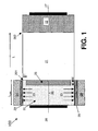
- FIG. 1 illustrates a cross-section of a TFET structure 100 according to an embodiment of the invention, the TFET structure comprising a source-channel-drain structure comprising a source region 30, a channel region 21 and a drain region 22 adjacent one another in longitudinal direction L of the device. Between the source region 30 and the channel region 21 a source-channel interface 201 is present. Between the drain region 22 and the channel region 21 a drain-channel interface 202 is present.
- the TFET structure as illustrated in FIG. 1 further comprises a gate electrode 24 which only overlaps with at least part of the source region 30.
- the source region 30 comprises a first source sub-region 20 and a second source sub-region 25.
- the gate electrode 24 does not overlap with the channel region 21 nor with the drain region 22.
- the TFET structure 100 in accordance with embodiments of the present invention and as illustrated in FIG. 1 further comprises a gate dielectric 29 in between the gate electrode 24 and the source region 30.
- the second source sub-region 25 is located at the source-channel interface of the TFET structure and has a width W in longitudinal direction L of the TFET structure 100.
- the width W of the second source sub-region 25 may for example be between one monolayer and 10 nm.
- the second source sub-region 25 has the same dopant type as the first source sub-region 20, however the peak concentration in the second source sub-region 25 is substantially higher than the maximum doping level of the doping profile of the first source sub-region 20 at or close to the interface between the first and the second source sub-regions 20, 25.
- the TFET structure 100 further comprises a source contact 26 electrically contacting the source region 30, and a drain contact 27 electrically contacting the drain region 22.
- the first source sub-region 20 may have a sloped (for example Gaussian) doping profile with a tail towards the source-channel interface 201.
- the second source sub-region 25 is then preferably located near, e.g. adjacent to, the source-channel interface 201 with a doping level which is substantially higher than the maximum doping level of the doping profile in the first source sub-region 20 close to the interface between the first and the second source sub-regions 20, 25.
- the gate electrode 24 may overlap the source region 30 completely or may overlap only part of the source region 30. However, in accordance with embodiments of the present invention, the gate electrode 24 may not overlap with the channel region 21 nor with the drain region 22 of the TFET device 100. By this configuration, line tunneling takes place rather than point tunneling.
- an underlap L underlap may be defined, which is the distance of the source region 30 which is not overlapped by the gate electrode 24.
- the underlap L underlap may be present at one side or both sides of the gate electrode 24 in longitudinal direction L, i.e. a first underlap at the side of the source-channel interface 201 and/or a second underlap at the source 20, 25 - source contact electrode 26 side.
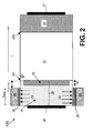
- FIG. 2 illustrates an example of an underlap L underlap being for this example the distance between the gate electrode 24 and the source-channel interface 201.
- the second source sub-region 25 may also be referred to as pocket region. Both first source sub-region 20 and second source sub-region 25 are doped with the same doping type, i.e. are both p-type (or alternatively n-type).
- the peak concentration of dopants, i.e. the maximum doping level, in the second source sub-region 25 should be substantially higher than the maximum doping level of the first doping profile close to the interface between the first and the second source sub-regions 20, 25.
- the peak concentration of the second source sub-region 25, also called the second peak concentration should be preferably at least a factor 4 higher than the maximum doping level of the first doping profile at or close to, e.g.
- the first source sub-region 20 may be doped substantially uniformly with dopants of a particular type, e.g. p-type dopants such as Boron, to a first peak concentration of 1e20/cm 3 .
- the second source sub-region 25 may be doped with a same type of dopants, e.g. also p-type dopants such as Boron, to a doping level at least four times higher than the doping level of the first source sub-region 20, e.g.
- the maximum doping level of the doping profile in the first source sub-region 20 at or close to the interface between the first and the second source sub-regions 20, 25 may vary depending on the first doping profile characteristics (such as peak concentration, steepness of slope of the doping profile,). Two examples are schematically shown in FIG. 9 and FIG. 10 .
- FIG. 9 and FIG. 10 schematically represent possible examples for the first and second doping profile of the first and second source sub-regions 20, 25 respectively, according to embodiments of the present invention.
- FIG. 9 shows a first doping profile 1011 with a first peak concentration 1021 in a first source sub-region 20 and a second doping profile 1012 with a second peak concentration 1022 in a second source sub-region 25.
- a source-channel interface 201 is shown as well as the interface 1014 between the first and the second source sub-regions.
- the second peak concentration 1022 should be higher than the maximum doping level of the first doping profile 1011 close to the interface 1014, here shown as the region between 1014 and 1015 wherein position 1015 is about 5 nm from the interface 1014. For this region in between position 1015 and interface 1014, a maximum doping level 1023 is defined.
- the second peak concentration 1022 must be substantially higher than the doping level 1023.
- FIG. 10 shows a similar situation as FIG. 9 , however the first doping profile 1011 of the first source sub-region 20 is a very abrupt doping profile, which can be seen by the steep slope of the profile 1011.
- the second peak concentration 1022 of the second doping profile 1012 should be higher than the maximum doping level 1023 of the first doping profile 1011 close to the interface 1014 between the first and second source sub-regions 20, 25, here shown as the region between 1014 and 1015 wherein position 1015 is about 5 nm from the interface 1014.
- the second peak concentration 1022 must be substantially higher than the first peak concentration 1021 of the first doping profile 1011.
- the drain region 22 is doped with an opposite doping type compared to the source region 30, e.g. n-type drain for a p-type source or vice versa.
- the doping level of the drain region 22 is preferably similar to the doping level of the first source sub-region 20, e.g. about 1e20/cm 3 .
- the channel region 21 in between may be lowly doped or undoped, e.g. doped at a doping level of 1e12/cm 3 to 1e15/cm 3 .
- the influence of the drain-source voltage V DS may be better controlled.
- the shift in drain-source current I DS is less at an applied gate voltage V G with varying drain-source voltage V DS compared to prior art TFETs without such second source sub-region. This prevents tunneling of charge carriers from the source region 30 to the channel region 21 as such enhancing the point tunneling current and contributing to the total tunneling current. Otherwise said, the pocket region 25 forms a barrier for carriers (electrons or holes) to flow between the source region 30 and channel region 21.
- the second source sub-region 25 or pocket region may be located directly in contact with the source-channel interface 201 (as illustrated in FIG. 1 and FIG. 2 ) or may be located at a distance D from the source-channel interface 201 (as illustrated in FIG. 3 ).
- the pocket region 25 is illustrated with a rectangular shape; however, this is only illustrative and also other more irregular shapes may be provided depending on the doping technique used.
- the second source sub-region 25 has a width W in longitudinal direction which may be in the range of a monolayer to 10 nm.
- the second source sub-region 25 may be, in a direction perpendicular to the longitudinal direction L, at a distance T from the gate dielectric 29. This distance T may be in the range of 0 to 10 nm, for example in the range between 0 to 5 nm, depending on the dimensions of the body (i.e. the dimensions of the source-channel-drain structure).
- Doping the second source sub-region 25 may be done by techniques as known for a person skilled in the art.
- a first implantation may be performed to dope the first source sub-region 20 with a first doping level and a second implantation may be performed to additionally dope the second source sub-region 25 with a second doping level higher than the first doping level.
- a vertical architecture of the TFET device i.e.
- the second source sub-region 25 may be formed by epitaxially growing a doped layer on top of the channel region 21 and thereafter another lower doped layer may be epitaxially grown on top of the second source sub-region 25 thereby forming the first source sub-region 20.
- Simulations as illustrated in FIG.4 , FIG.5 and FIG. 6 are performed with device simulator Sentaurus Device from Synopsys ® to determine the characteristics of a TFET structure 100 according to embodiments of the present invention.
- the TFET structure 100 used for the simulation is shown in FIG. 1 with the gate electrode completely covering the source region 30.
- the TFET structure is 2-dimensional and is a double-gate structure with a gate at both sides (e.g. top and bottom as illustrated in FIG. 1 ) of the source region 30.
- the height of the central part of the source region 30 (between the gate dielectrics 29) is 50 nm.
- the equivalent oxide thickness EOT of the gate dielectric 29 is varied from 0.4 nm up to 1.2 nm.
- the length of the channel region 21 is 40 nm, and the length of the gate 24 is 30 nm (no overlap with the channel region 21).
- the most important dimensions in the TFET structure 100 to be taken into account for the electrical performance are the length of the gate L gate and the thickness and doping level of the second source sub-region (pocket region) 25.
- the doping of the (first and second) source sub-regions 20, 25 and of the drain region 22 is in the example p-type doping, the doping level is 1e20/cm 3 .
- the doping of the second source sub-region 25 is in the example p-type doping, the doping level is 4e20/cm 3 .
- the doping of the drain region 22 is in the example n-type doping, the doping level is 1e20/cm 3 .
- the doping of the channel region 21 is not critical, as long as it is lowly doped.
- the doping level for the channel region used in this simulation example is n-type, 10 13 /cm 3 .
- FIG. 4 The reduced influence of the drain-source voltage V DS due to the presence of the higher doped second source sub-region 25 is illustrated also in FIG. 4 , FIG. 5 and FIG. 6 which show simulated results for TFET structure according to embodiments of the present invention.
- FIG.4 illustrates simulated output characteristics for a TFET structure without a second source sub-region in the source region and with the gate only present on the source region.
- FIG.4 illustrates the drain currents I DS versus gate voltage V GS for different drain voltages V DS .
- the source region consists of a first source sub-region only and has a doping level of 1e20/cm 3 .
- a gate dielectric is present in between the gate and the source region with an equivalent oxide thickness EOT of 0.4 nm.
- the drain region has a doping level of 1e20/cm 3 and the channel region has a doping level of 1e13/cm 3 .
- the gate-source voltage V GS is shifted with approximately 50mV when changing the drain voltage V DS from 0.1V up to 1V.
- the gate-source voltage V GS at 10fA/um (onset voltage) is shifted approximately 0.1V when changing the drain voltage V DS from 0.1V up to 1V. This is however detrimental, hence not wanted, since it will influence the performance (negative impact) of the TFET in a circuit.
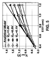
- FIG. 5 illustrates simulated input characteristics for a TFET structure 100 with a second (pocket) source sub-region 25 (closed symbols) according to embodiments of the present invention and compares these to input characteristics of a TFET structure without a second (pocket) source sub-region (open symbols).
- the gate 24 is only present on the source region 30.
- a 3 nm wide second (pocket) source sub-region 25 with a doping level of 4e20/cm 3 is used.
- V onset defined as the gate-source voltage required to obtain a current of 10 fA/ ⁇ m, in function of the equivalent oxide thickness EOT of the gate dielectric 29 which is present in between the gate 24 and the source region 30 for different drain voltages V DS (0.1V, 0.5V and 1V).
- V DS 0.1V, 0.5V and 1V.
- the spread in V onset for different drain voltages V DS is becoming smaller for smaller EOT.
- V onset becomes independent of the drain voltage V DS for small EOT, i.e. for EOT smaller than 0.6 nm.
- EOT i.e. for EOT higher than 0.6 nm
- the spread of V onset is almost comparable for a TFET structure with or without a second (pocket) source sub-region 25.
- this is: it is expected that it is always possible to decrease the spread in the gate-source voltage upon varying the drain-source voltage by introducing a pocket in accordance with embodiments of the present invention.
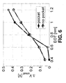
- FIG. 6 illustrates simulated input characteristics for a TFET structure 100 with a second (pocket) source sub-region 25 (closed symbols) according to embodiments of the present invention and without a second (pocket) source sub-region (open symbols).
- the gate 24 is only present on the source region 30.
- a 3 nm wide second (pocket) source sub-region 25 with a doping level of 4e20/cm 3 is used.
- ⁇ V onset can be significantly reduced (nearly becomes 0) for a TFET structure with a second (pocket) source sub-region 25 (closed symbols) according to embodiments of the present invention.
- a method 300 is provided for manufacturing a TFET structure according to embodiments of the present invention.
- FIG. 8 A particular processing method to fabricate a TFET structure is illustrated in the flowchart shown in FIG. 8 .
- the method 300 according to an embodiment of the invention will be illustrated for a TFET comprising one (double) gate structure as shown in FIG. 1 (cross section). It has to be understood that this is not limiting the invention and that the method may also be applied to create alternative TFET structures (e.g. comprising a nanowire, a second gate structure,...) in accordance with embodiments of the present invention, for example as described above.
- a substrate is provided.
- said substrate is a semiconductor substrate such as a silicon substrate or a silicon on insulator (SOI) substrate but any other suitable substrate can be used as well such as, for example, glass, ceramics, etc.
- SOI silicon on insulator
- a source-channel-drain structure having at least one n (or p) doped drain region 22, one channel region 21, and one p (or n) doped source region 30 comprising a first and second doped source sub-region 20, 25 is formed.
- Deposition techniques such as, for example, CVD (Chemical Vapor Deposition), MOCVD (Metal Organic Chemical Vapor Deposition), or PECVD (plasma enhanced chemical vapor deposition) processes can be used.
- CVD Chemical Vapor Deposition
- MOCVD Metal Organic Chemical Vapor Deposition
- PECVD plasma enhanced chemical vapor deposition
- etching techniques can be used whereby said structures are etched into the substrate.
- the different regions with different doping levels and different doping types need to be created to form the drain region 22, the channel region 21 and the source region 30 (first and second source sub-regions 20, 25) in the source-channel-drain structure.
- These different regions can be doped during the deposition process to obtain a n-type or p-type region.
- the doping may be performed after the deposition step by means of an additional doping step - as illustrated for example in steps 316, 317, 318 of the method.
- the doping in one specific region, e.g. first source sub-region 22, second source sub-region 25 or drain region 22 may be uniform, or may alternatively have a non-uniform doping profile.
- Doping the source region 30 comprises doping a first source sub-region 20 with a first doping type and a first doping level and doping a second source sub-region 25 with a second doping type being the same as the first doping type and with a second doping level being substantially higher than the first doping level.
- the source-channel-drain structure created is a vertical structure.
- a drain region 22 is created on the substrate ⁇ step 311.
- Said drain region 22 may be made of a first semiconductor material which is highly n doped in case of a n-type TFET, or alternatively in case of a p-type TFET said drain region 22 is highly p doped.
- the doping level of the drain region 22 is in the range of 1e18/cm 3 to 1e21/cm 3 , for example in the range of 1e19/cm 3 to 5e20/cm 3 .
- the channel region 21 of the TFET is formed onto the drain region 22, thereby forming a drain-channel interface 202 ⁇ step 312.
- said channel region 21 may preferably be made of the first semiconductor material, although other suitable/compatible materials can be used.
- the doping level of the channel region 21 may be in the range of undoped up to 1e17/cm 3 doping, for example in the range of undoped up to 1e14/cm 3 doping.
- a source region 30 is created next to the channel region 21, thereby forming a source-channel interface 201 ⁇ step 313.
- Said source region 30 may be made of the first semiconductor material, although other suitable/compatible materials can be used.
- the semiconductor material may be highly p doped in case of a n-type TFET (or alternatively in case of a p-type TFET said source region 30 may be highly n doped).
- the source region 30 comprises a first source sub-region 20 with a first doping type and doping level and a second source sub-region 25 with a second doping type being the same as the first doping type and with a second doping level being substantially higher than the first doping level.
- the doping level of the first source sub-region 20 may be in the range of 1e18/cm 3 to 1e21/cm 3 , for example in the range of 1e19/cm 3 to 5e20/cm 3 .
- the doping level of the second source sub-region 25 may be in the range of 5e18/cm 3 to 4e21/cm 3 , for example in the range of 2e19/cm 3 to 1e21/cm 3 .
- n-TFET n-TFET
- p-TFET n-TFET
- possible p-type dopants are B, Al, Ga, ln, Tl, Pd, Na, Be, Zn, Au, Co, V, Ni, MO, Hg, Sr, Ge, Cu, K, Sn, W, Pb, O, Fe
- possible n-type dopants are Li, Sb, P, As, Bi, Te, Ti, C, Mg, Se, Cr, Ta, Cs, Ba, S, Mn, Ag, Cd, Pt.
- Possible p-type dopants are B, Al, TI, Ga, In, Be, Zn, Cr, Cd, Hg, Co, Ni, Mn, Fe, Ptl; and possible n-type dopants are Li, Sb, P, As, S, Se, Te, Cu, Au, Ag.
- a gate electrode 24 is formed on the source region 30, covering at least part of the source region 30 in a longitudinal direction L such that there is no coverage by the gate electrode 24 of the channel region 21 nor of the drain region 22, more specifically a single gate, double gate or triple gate structure can be formed depending on the type of TFET (planar, MUGFET, horizontal,..).
- a gate dielectric (e.g. oxide) 29 is deposited- step 315. Said gate dielectric 29 is at least situated below the whole length of the gate electrode 24 but can cover up to the whole length of the TFET structure, i.e. of the underlying source-channel-drain structure.
- a gate electrode 24 is deposited on top of said gate dielectric 29.
- the gate dielectric 29 may be selected from at least one of silicon based oxides (e.g. silicon dioxide, silicon oxy nitride), aluminium oxide, high-k oxides (oxides, nitrided oxides, silicates and nitrided silicates of transition metals such as Hf, Ta, Ti, Nb, V, Y, Zr).
- silicon based oxides e.g. silicon dioxide, silicon oxy nitride
- aluminium oxide high-k oxides (oxides, nitrided oxides, silicates and nitrided silicates of transition metals such as Hf, Ta, Ti, Nb, V, Y, Zr).
- high-k oxides oxides, nitrided oxides, silicates and nitrided silicates of transition metals such as Hf, Ta, Ti, Nb, V, Y, Zr.
- said gate dielectric is a high-k oxide such as hafnium
- the gate electrode 24 may be made of a conductive material, for example selected from at least one of poly silicon, poly germanium, metals such as Al, W, Ta, Ti, Ru, Pd, Rh, Re, Pt, and alloys thereof, metal-nitrides such as TaN and TiN, metal-silicon nitrides such as TaSiN, conductive oxides such as RuO 2 and ReO 3 fully silicided metals (FUSI) such as CoSi 2 , NiSi and TiSi 2 , fully germanided metals (FUGE), workfunction tunable metals, engineered materials to obtain a particular gate workfunction.
- said gate electrode 24 is made of a metal of which the workfunction has been engineered specifically for the chosen channel material 21, the gate dielectric material, gate dielectric thickness and channel doping.
- an electrical contact 26, 27 may be formed on the source region 30 and/or on the drain region 22.
- Said electrical contact 26, 27 may be a conductive material which is selected from at least one of a silicide containing structure (NiSi, CoSi 2 , TiSi 2 ,...), a germanide containing structure, a metal containing structure, poly silicon or a combination thereof.
- said electrical contact may be a combination of a metal with a silicide.
- the source and/or drain contact 27 may be a silicide containing structure.
Landscapes
- Engineering & Computer Science (AREA)
- Chemical & Material Sciences (AREA)
- Nanotechnology (AREA)
- Physics & Mathematics (AREA)
- Mathematical Physics (AREA)
- Theoretical Computer Science (AREA)
- Crystallography & Structural Chemistry (AREA)
- Thin Film Transistor (AREA)
- Insulated Gate Type Field-Effect Transistor (AREA)
Priority Applications (2)
| Application Number | Priority Date | Filing Date | Title |
|---|---|---|---|
| US13/474,526 US8629428B2 (en) | 2011-05-23 | 2012-05-17 | Line-tunneling tunnel field-effect transistor (TFET) and manufacturing method |
| JP2012114056A JP6013777B2 (ja) | 2011-05-23 | 2012-05-18 | ライントンネリングトンネル電界効果トランジスタ(tfet)及びその製造方法 |
Applications Claiming Priority (1)
| Application Number | Priority Date | Filing Date | Title |
|---|---|---|---|
| US201161488934P | 2011-05-23 | 2011-05-23 |
Publications (2)
| Publication Number | Publication Date |
|---|---|
| EP2528099A1 EP2528099A1 (en) | 2012-11-28 |
| EP2528099B1 true EP2528099B1 (en) | 2015-03-04 |
Family
ID=45715334
Family Applications (1)
| Application Number | Title | Priority Date | Filing Date |
|---|---|---|---|
| EP11173950.4A Active EP2528099B1 (en) | 2011-05-23 | 2011-07-14 | Line- tunneling Tunnel Field-Effect Transistor (TFET) and manufacturing method |
Country Status (3)
| Country | Link |
|---|---|
| US (1) | US8629428B2 (enExample) |
| EP (1) | EP2528099B1 (enExample) |
| JP (1) | JP6013777B2 (enExample) |
Cited By (1)
| Publication number | Priority date | Publication date | Assignee | Title |
|---|---|---|---|---|
| CN105390531A (zh) * | 2015-10-27 | 2016-03-09 | 北京大学 | 一种隧穿场效应晶体管的制备方法 |
Families Citing this family (23)
| Publication number | Priority date | Publication date | Assignee | Title |
|---|---|---|---|---|
| CN102664165B (zh) * | 2012-05-18 | 2014-06-04 | 北京大学 | 基于标准cmos ic工艺制备互补隧穿场效应晶体管的方法 |
| US9209288B2 (en) | 2012-12-21 | 2015-12-08 | Intel Corporation | Reduced scale resonant tunneling field effect transistor |
| JP6083704B2 (ja) * | 2013-03-25 | 2017-02-22 | 国立研究開発法人産業技術総合研究所 | トンネルfetのデバイスシミュレーション方法及びシステム並びにトンネルfetのコンパクトモデル設計方法及びコンパクトモデル |
| US9634114B2 (en) | 2013-08-13 | 2017-04-25 | National University Corporation Hakkaido University | Tunnel field-effect transistor, method for manufacturing same, and switch element |
| JP5886802B2 (ja) | 2013-08-29 | 2016-03-16 | 株式会社東芝 | 半導体装置 |
| CN103474459B (zh) * | 2013-09-06 | 2016-01-27 | 北京大学深圳研究生院 | 隧穿场效应晶体管 |
| JP6083707B2 (ja) * | 2013-09-09 | 2017-02-22 | 国立研究開発法人産業技術総合研究所 | 半導体装置およびその製造方法 |
| CN103560144B (zh) * | 2013-11-13 | 2016-02-17 | 北京大学 | 抑制隧穿晶体管泄漏电流的方法及相应的器件和制备方法 |
| US9419114B2 (en) * | 2014-01-17 | 2016-08-16 | Imec Vzw | Tunnel field-effect transistor |
| US9281363B2 (en) | 2014-04-18 | 2016-03-08 | Taiwan Semiconductor Manufacturing Company Ltd. | Circuits using gate-all-around technology |
| EP2993696B1 (en) * | 2014-09-02 | 2020-08-05 | IMEC vzw | Heterosection tunnel field-effect transistor (TFET) |
| KR102154185B1 (ko) | 2014-09-19 | 2020-09-09 | 삼성전자 주식회사 | 반도체 소자 |
| EP3010044B1 (en) | 2014-10-13 | 2019-02-13 | IMEC vzw | Layered structure of a p-TFET |
| US10504721B2 (en) | 2015-04-30 | 2019-12-10 | Taiwan Semiconductor Manufacturing Company, Ltd. | Staggered-type tunneling field effect transistor |
| US9526436B2 (en) | 2015-05-19 | 2016-12-27 | Samsung Electronics Co., Ltd | Amplifiers including tunable tunnel field effect transistor pseudo resistors and related devices |
| JP6487288B2 (ja) * | 2015-07-17 | 2019-03-20 | 国立大学法人東北大学 | 電界効果トランジスタおよびその駆動方法 |
| US9735267B1 (en) | 2016-01-28 | 2017-08-15 | Taiwan Semiconductor Manufacturing Co., Ltd. | Structure and formation method of semiconductor device structure |
| US10141436B2 (en) * | 2016-04-04 | 2018-11-27 | Purdue Research Foundation | Tunnel field effect transistor having anisotropic effective mass channel |
| CN108780812B (zh) * | 2016-06-30 | 2020-10-16 | 华为技术有限公司 | 隧穿场效应晶体管及其制备方法 |
| US10236386B2 (en) | 2017-01-17 | 2019-03-19 | The Board Of Trustees Of The University Of Illinois | Vertical hetero- and homo-junction tunnel field-effect transistors |
| US10475908B2 (en) * | 2017-04-25 | 2019-11-12 | Taiwan Semiconductor Manufacturing Co., Ltd. | Semiconductor device and method of fabricating the same |
| WO2019005113A1 (en) * | 2017-06-30 | 2019-01-03 | Intel Corporation | RESISTIVE LIVE MEMORY COMPRISING A TUNNEL SOURCE ACCESS TRANSISTOR |
| CN110379851B (zh) * | 2019-06-17 | 2023-01-10 | 宁波大学 | 一种基于tfet的三输入多数逻辑器件 |
Family Cites Families (3)
| Publication number | Priority date | Publication date | Assignee | Title |
|---|---|---|---|---|
| US7329937B2 (en) * | 2005-04-27 | 2008-02-12 | International Business Machines Corporation | Asymmetric field effect transistors (FETs) |
| EP1900681B1 (en) * | 2006-09-15 | 2017-03-15 | Imec | Tunnel Field-Effect Transistors based on silicon nanowires |
| US8120115B2 (en) | 2007-03-12 | 2012-02-21 | Imec | Tunnel field-effect transistor with gated tunnel barrier |
-
2011
- 2011-07-14 EP EP11173950.4A patent/EP2528099B1/en active Active
-
2012
- 2012-05-17 US US13/474,526 patent/US8629428B2/en not_active Expired - Fee Related
- 2012-05-18 JP JP2012114056A patent/JP6013777B2/ja active Active
Cited By (2)
| Publication number | Priority date | Publication date | Assignee | Title |
|---|---|---|---|---|
| CN105390531A (zh) * | 2015-10-27 | 2016-03-09 | 北京大学 | 一种隧穿场效应晶体管的制备方法 |
| CN105390531B (zh) * | 2015-10-27 | 2018-02-13 | 北京大学 | 一种隧穿场效应晶体管的制备方法 |
Also Published As
| Publication number | Publication date |
|---|---|
| JP2013012723A (ja) | 2013-01-17 |
| US20120298959A1 (en) | 2012-11-29 |
| US8629428B2 (en) | 2014-01-14 |
| JP6013777B2 (ja) | 2016-10-25 |
| EP2528099A1 (en) | 2012-11-28 |
Similar Documents
| Publication | Publication Date | Title |
|---|---|---|
| EP2528099B1 (en) | Line- tunneling Tunnel Field-Effect Transistor (TFET) and manufacturing method | |
| US9741848B2 (en) | Multi-gate tunnel field-effect transistor (TFET) | |
| US8120115B2 (en) | Tunnel field-effect transistor with gated tunnel barrier | |
| US8148220B2 (en) | Tunnel effect transistors based on elongate monocrystalline nanostructures having a heterostructure | |
| US9318583B2 (en) | Tunnel field effect transistor and method for making thereof | |
| EP2309544B1 (en) | Tunnel field effect transistor with improved subthreshold swing | |
| US8587075B2 (en) | Tunnel field-effect transistor with metal source | |
| EP1901354B1 (en) | A tunnel field-effect transistor with gated tunnel barrier | |
| CN103582930B (zh) | 具有凹陷沟道膜和突变结的mosfet | |
| KR102157825B1 (ko) | 터널링 전계 효과 트랜지스터 | |
| EP2993696B1 (en) | Heterosection tunnel field-effect transistor (TFET) | |
| TWI613830B (zh) | 穿隧式場效電晶體及製造此種電晶體之方法 | |
| WO2012152762A1 (en) | Tunnel field effect transistor device | |
| US20200098862A1 (en) | Metal source/drain-based mosfet and method for fabricating the same | |
| US20220123110A1 (en) | Vertical tunnel field-effect transistor with u-shaped gate and band aligner | |
| US10211287B2 (en) | Layered structure of a P-TFET | |
| KR20150085663A (ko) | 터널링 전계 효과 트랜지스터 | |
| KR102273935B1 (ko) | 음성 트랜스 컨덕턴스 기반의 터널링 트랜지스터 | |
| EP1901355B1 (en) | Tunnel effect transistors based on monocrystalline nanowires having a heterostructure |
Legal Events
| Date | Code | Title | Description |
|---|---|---|---|
| PUAI | Public reference made under article 153(3) epc to a published international application that has entered the european phase |
Free format text: ORIGINAL CODE: 0009012 |
|
| AK | Designated contracting states |
Kind code of ref document: A1 Designated state(s): AL AT BE BG CH CY CZ DE DK EE ES FI FR GB GR HR HU IE IS IT LI LT LU LV MC MK MT NL NO PL PT RO RS SE SI SK SM TR |
|
| AX | Request for extension of the european patent |
Extension state: BA ME |
|
| 17P | Request for examination filed |
Effective date: 20130527 |
|
| RBV | Designated contracting states (corrected) |
Designated state(s): AL AT BE BG CH CY CZ DE DK EE ES FI FR GB GR HR HU IE IS IT LI LT LU LV MC MK MT NL NO PL PT RO RS SE SI SK SM TR |
|
| GRAP | Despatch of communication of intention to grant a patent |
Free format text: ORIGINAL CODE: EPIDOSNIGR1 |
|
| INTG | Intention to grant announced |
Effective date: 20141002 |
|
| GRAS | Grant fee paid |
Free format text: ORIGINAL CODE: EPIDOSNIGR3 |
|
| GRAA | (expected) grant |
Free format text: ORIGINAL CODE: 0009210 |
|
| AK | Designated contracting states |
Kind code of ref document: B1 Designated state(s): AL AT BE BG CH CY CZ DE DK EE ES FI FR GB GR HR HU IE IS IT LI LT LU LV MC MK MT NL NO PL PT RO RS SE SI SK SM TR |
|
| REG | Reference to a national code |
Ref country code: GB Ref legal event code: FG4D |
|
| REG | Reference to a national code |
Ref country code: CH Ref legal event code: EP |
|
| REG | Reference to a national code |
Ref country code: IE Ref legal event code: FG4D |
|
| REG | Reference to a national code |
Ref country code: AT Ref legal event code: REF Ref document number: 714525 Country of ref document: AT Kind code of ref document: T Effective date: 20150415 |
|
| REG | Reference to a national code |
Ref country code: DE Ref legal event code: R096 Ref document number: 602011014263 Country of ref document: DE Effective date: 20150416 |
|
| REG | Reference to a national code |
Ref country code: FR Ref legal event code: PLFP Year of fee payment: 5 |
|
| REG | Reference to a national code |
Ref country code: AT Ref legal event code: MK05 Ref document number: 714525 Country of ref document: AT Kind code of ref document: T Effective date: 20150304 Ref country code: NL Ref legal event code: VDEP Effective date: 20150304 |
|
| PG25 | Lapsed in a contracting state [announced via postgrant information from national office to epo] |
Ref country code: FI Free format text: LAPSE BECAUSE OF FAILURE TO SUBMIT A TRANSLATION OF THE DESCRIPTION OR TO PAY THE FEE WITHIN THE PRESCRIBED TIME-LIMIT Effective date: 20150304 Ref country code: HR Free format text: LAPSE BECAUSE OF FAILURE TO SUBMIT A TRANSLATION OF THE DESCRIPTION OR TO PAY THE FEE WITHIN THE PRESCRIBED TIME-LIMIT Effective date: 20150304 Ref country code: LT Free format text: LAPSE BECAUSE OF FAILURE TO SUBMIT A TRANSLATION OF THE DESCRIPTION OR TO PAY THE FEE WITHIN THE PRESCRIBED TIME-LIMIT Effective date: 20150304 Ref country code: NO Free format text: LAPSE BECAUSE OF FAILURE TO SUBMIT A TRANSLATION OF THE DESCRIPTION OR TO PAY THE FEE WITHIN THE PRESCRIBED TIME-LIMIT Effective date: 20150604 Ref country code: SE Free format text: LAPSE BECAUSE OF FAILURE TO SUBMIT A TRANSLATION OF THE DESCRIPTION OR TO PAY THE FEE WITHIN THE PRESCRIBED TIME-LIMIT Effective date: 20150304 Ref country code: ES Free format text: LAPSE BECAUSE OF FAILURE TO SUBMIT A TRANSLATION OF THE DESCRIPTION OR TO PAY THE FEE WITHIN THE PRESCRIBED TIME-LIMIT Effective date: 20150304 |
|
| REG | Reference to a national code |
Ref country code: LT Ref legal event code: MG4D |
|
| PG25 | Lapsed in a contracting state [announced via postgrant information from national office to epo] |
Ref country code: AT Free format text: LAPSE BECAUSE OF FAILURE TO SUBMIT A TRANSLATION OF THE DESCRIPTION OR TO PAY THE FEE WITHIN THE PRESCRIBED TIME-LIMIT Effective date: 20150304 Ref country code: RS Free format text: LAPSE BECAUSE OF FAILURE TO SUBMIT A TRANSLATION OF THE DESCRIPTION OR TO PAY THE FEE WITHIN THE PRESCRIBED TIME-LIMIT Effective date: 20150304 Ref country code: LV Free format text: LAPSE BECAUSE OF FAILURE TO SUBMIT A TRANSLATION OF THE DESCRIPTION OR TO PAY THE FEE WITHIN THE PRESCRIBED TIME-LIMIT Effective date: 20150304 Ref country code: GR Free format text: LAPSE BECAUSE OF FAILURE TO SUBMIT A TRANSLATION OF THE DESCRIPTION OR TO PAY THE FEE WITHIN THE PRESCRIBED TIME-LIMIT Effective date: 20150605 |
|
| PG25 | Lapsed in a contracting state [announced via postgrant information from national office to epo] |
Ref country code: NL Free format text: LAPSE BECAUSE OF FAILURE TO SUBMIT A TRANSLATION OF THE DESCRIPTION OR TO PAY THE FEE WITHIN THE PRESCRIBED TIME-LIMIT Effective date: 20150304 |
|
| PG25 | Lapsed in a contracting state [announced via postgrant information from national office to epo] |
Ref country code: CZ Free format text: LAPSE BECAUSE OF FAILURE TO SUBMIT A TRANSLATION OF THE DESCRIPTION OR TO PAY THE FEE WITHIN THE PRESCRIBED TIME-LIMIT Effective date: 20150304 Ref country code: RO Free format text: LAPSE BECAUSE OF FAILURE TO SUBMIT A TRANSLATION OF THE DESCRIPTION OR TO PAY THE FEE WITHIN THE PRESCRIBED TIME-LIMIT Effective date: 20150304 Ref country code: SK Free format text: LAPSE BECAUSE OF FAILURE TO SUBMIT A TRANSLATION OF THE DESCRIPTION OR TO PAY THE FEE WITHIN THE PRESCRIBED TIME-LIMIT Effective date: 20150304 Ref country code: EE Free format text: LAPSE BECAUSE OF FAILURE TO SUBMIT A TRANSLATION OF THE DESCRIPTION OR TO PAY THE FEE WITHIN THE PRESCRIBED TIME-LIMIT Effective date: 20150304 Ref country code: PT Free format text: LAPSE BECAUSE OF FAILURE TO SUBMIT A TRANSLATION OF THE DESCRIPTION OR TO PAY THE FEE WITHIN THE PRESCRIBED TIME-LIMIT Effective date: 20150706 |
|
| PG25 | Lapsed in a contracting state [announced via postgrant information from national office to epo] |
Ref country code: IS Free format text: LAPSE BECAUSE OF FAILURE TO SUBMIT A TRANSLATION OF THE DESCRIPTION OR TO PAY THE FEE WITHIN THE PRESCRIBED TIME-LIMIT Effective date: 20150704 Ref country code: PL Free format text: LAPSE BECAUSE OF FAILURE TO SUBMIT A TRANSLATION OF THE DESCRIPTION OR TO PAY THE FEE WITHIN THE PRESCRIBED TIME-LIMIT Effective date: 20150304 |
|
| REG | Reference to a national code |
Ref country code: DE Ref legal event code: R097 Ref document number: 602011014263 Country of ref document: DE |
|
| PG25 | Lapsed in a contracting state [announced via postgrant information from national office to epo] |
Ref country code: IT Free format text: LAPSE BECAUSE OF FAILURE TO SUBMIT A TRANSLATION OF THE DESCRIPTION OR TO PAY THE FEE WITHIN THE PRESCRIBED TIME-LIMIT Effective date: 20150304 |
|
| PLBE | No opposition filed within time limit |
Free format text: ORIGINAL CODE: 0009261 |
|
| STAA | Information on the status of an ep patent application or granted ep patent |
Free format text: STATUS: NO OPPOSITION FILED WITHIN TIME LIMIT |
|
| PG25 | Lapsed in a contracting state [announced via postgrant information from national office to epo] |
Ref country code: DK Free format text: LAPSE BECAUSE OF FAILURE TO SUBMIT A TRANSLATION OF THE DESCRIPTION OR TO PAY THE FEE WITHIN THE PRESCRIBED TIME-LIMIT Effective date: 20150304 |
|
| 26N | No opposition filed |
Effective date: 20151207 |
|
| PG25 | Lapsed in a contracting state [announced via postgrant information from national office to epo] |
Ref country code: SI Free format text: LAPSE BECAUSE OF FAILURE TO SUBMIT A TRANSLATION OF THE DESCRIPTION OR TO PAY THE FEE WITHIN THE PRESCRIBED TIME-LIMIT Effective date: 20150304 Ref country code: MC Free format text: LAPSE BECAUSE OF FAILURE TO SUBMIT A TRANSLATION OF THE DESCRIPTION OR TO PAY THE FEE WITHIN THE PRESCRIBED TIME-LIMIT Effective date: 20150304 |
|
| REG | Reference to a national code |
Ref country code: CH Ref legal event code: PL |
|
| GBPC | Gb: european patent ceased through non-payment of renewal fee |
Effective date: 20150714 |
|
| PG25 | Lapsed in a contracting state [announced via postgrant information from national office to epo] |
Ref country code: LU Free format text: LAPSE BECAUSE OF FAILURE TO SUBMIT A TRANSLATION OF THE DESCRIPTION OR TO PAY THE FEE WITHIN THE PRESCRIBED TIME-LIMIT Effective date: 20150714 |
|
| REG | Reference to a national code |
Ref country code: IE Ref legal event code: MM4A |
|
| PG25 | Lapsed in a contracting state [announced via postgrant information from national office to epo] |
Ref country code: LI Free format text: LAPSE BECAUSE OF NON-PAYMENT OF DUE FEES Effective date: 20150731 Ref country code: CH Free format text: LAPSE BECAUSE OF NON-PAYMENT OF DUE FEES Effective date: 20150731 Ref country code: GB Free format text: LAPSE BECAUSE OF NON-PAYMENT OF DUE FEES Effective date: 20150714 |
|
| REG | Reference to a national code |
Ref country code: FR Ref legal event code: PLFP Year of fee payment: 6 |
|
| PG25 | Lapsed in a contracting state [announced via postgrant information from national office to epo] |
Ref country code: IE Free format text: LAPSE BECAUSE OF NON-PAYMENT OF DUE FEES Effective date: 20150714 |
|
| PG25 | Lapsed in a contracting state [announced via postgrant information from national office to epo] |
Ref country code: BE Free format text: LAPSE BECAUSE OF FAILURE TO SUBMIT A TRANSLATION OF THE DESCRIPTION OR TO PAY THE FEE WITHIN THE PRESCRIBED TIME-LIMIT Effective date: 20150304 |
|
| PG25 | Lapsed in a contracting state [announced via postgrant information from national office to epo] |
Ref country code: MT Free format text: LAPSE BECAUSE OF FAILURE TO SUBMIT A TRANSLATION OF THE DESCRIPTION OR TO PAY THE FEE WITHIN THE PRESCRIBED TIME-LIMIT Effective date: 20150304 |
|
| PG25 | Lapsed in a contracting state [announced via postgrant information from national office to epo] |
Ref country code: BG Free format text: LAPSE BECAUSE OF FAILURE TO SUBMIT A TRANSLATION OF THE DESCRIPTION OR TO PAY THE FEE WITHIN THE PRESCRIBED TIME-LIMIT Effective date: 20150304 Ref country code: SM Free format text: LAPSE BECAUSE OF FAILURE TO SUBMIT A TRANSLATION OF THE DESCRIPTION OR TO PAY THE FEE WITHIN THE PRESCRIBED TIME-LIMIT Effective date: 20150304 Ref country code: HU Free format text: LAPSE BECAUSE OF FAILURE TO SUBMIT A TRANSLATION OF THE DESCRIPTION OR TO PAY THE FEE WITHIN THE PRESCRIBED TIME-LIMIT; INVALID AB INITIO Effective date: 20110714 |
|
| REG | Reference to a national code |
Ref country code: FR Ref legal event code: PLFP Year of fee payment: 7 |
|
| PG25 | Lapsed in a contracting state [announced via postgrant information from national office to epo] |
Ref country code: CY Free format text: LAPSE BECAUSE OF FAILURE TO SUBMIT A TRANSLATION OF THE DESCRIPTION OR TO PAY THE FEE WITHIN THE PRESCRIBED TIME-LIMIT Effective date: 20150304 |
|
| PG25 | Lapsed in a contracting state [announced via postgrant information from national office to epo] |
Ref country code: TR Free format text: LAPSE BECAUSE OF FAILURE TO SUBMIT A TRANSLATION OF THE DESCRIPTION OR TO PAY THE FEE WITHIN THE PRESCRIBED TIME-LIMIT Effective date: 20150304 |
|
| REG | Reference to a national code |
Ref country code: FR Ref legal event code: PLFP Year of fee payment: 8 |
|
| PG25 | Lapsed in a contracting state [announced via postgrant information from national office to epo] |
Ref country code: MK Free format text: LAPSE BECAUSE OF FAILURE TO SUBMIT A TRANSLATION OF THE DESCRIPTION OR TO PAY THE FEE WITHIN THE PRESCRIBED TIME-LIMIT Effective date: 20150304 |
|
| PG25 | Lapsed in a contracting state [announced via postgrant information from national office to epo] |
Ref country code: AL Free format text: LAPSE BECAUSE OF FAILURE TO SUBMIT A TRANSLATION OF THE DESCRIPTION OR TO PAY THE FEE WITHIN THE PRESCRIBED TIME-LIMIT Effective date: 20150304 |
|
| P01 | Opt-out of the competence of the unified patent court (upc) registered |
Effective date: 20230513 |
|
| REG | Reference to a national code |
Ref country code: DE Ref legal event code: R079 Ref document number: 602011014263 Country of ref document: DE Free format text: PREVIOUS MAIN CLASS: H01L0029739000 Ipc: H10D0012000000 |
|
| PGFP | Annual fee paid to national office [announced via postgrant information from national office to epo] |
Ref country code: FR Payment date: 20250620 Year of fee payment: 15 |
|
| PGFP | Annual fee paid to national office [announced via postgrant information from national office to epo] |
Ref country code: DE Payment date: 20250620 Year of fee payment: 15 |