EP2523777B1 - Cmp pad with local area transparency - Google Patents
Cmp pad with local area transparency Download PDFInfo
- Publication number
- EP2523777B1 EP2523777B1 EP11700493.7A EP11700493A EP2523777B1 EP 2523777 B1 EP2523777 B1 EP 2523777B1 EP 11700493 A EP11700493 A EP 11700493A EP 2523777 B1 EP2523777 B1 EP 2523777B1
- Authority
- EP
- European Patent Office
- Prior art keywords
- polishing
- lat
- pad
- opaque
- polyurea
- Prior art date
- Legal status (The legal status is an assumption and is not a legal conclusion. Google has not performed a legal analysis and makes no representation as to the accuracy of the status listed.)
- Active
Links
- 238000005498 polishing Methods 0.000 claims description 157
- 239000010410 layer Substances 0.000 claims description 55
- 239000000463 material Substances 0.000 claims description 49
- 238000000034 method Methods 0.000 claims description 47
- 239000004814 polyurethane Substances 0.000 claims description 27
- 229920002396 Polyurea Polymers 0.000 claims description 25
- 229920003226 polyurethane urea Polymers 0.000 claims description 23
- 229920001187 thermosetting polymer Polymers 0.000 claims description 21
- 239000012790 adhesive layer Substances 0.000 claims description 17
- 238000000748 compression moulding Methods 0.000 claims description 12
- 238000011065 in-situ storage Methods 0.000 claims description 11
- 238000004519 manufacturing process Methods 0.000 claims description 11
- -1 polyethylene Polymers 0.000 claims description 11
- 239000007788 liquid Substances 0.000 claims description 10
- 238000012544 monitoring process Methods 0.000 claims description 10
- 238000001514 detection method Methods 0.000 claims description 9
- 239000004820 Pressure-sensitive adhesive Substances 0.000 claims description 6
- 239000004698 Polyethylene Substances 0.000 claims description 3
- 229920000573 polyethylene Polymers 0.000 claims description 3
- 229920001721 polyimide Polymers 0.000 claims description 3
- 239000003822 epoxy resin Substances 0.000 claims description 2
- 229920000647 polyepoxide Polymers 0.000 claims description 2
- 230000005540 biological transmission Effects 0.000 claims 1
- 229930186657 Lat Natural products 0.000 description 140
- 239000000758 substrate Substances 0.000 description 39
- 239000000203 mixture Substances 0.000 description 22
- 230000008569 process Effects 0.000 description 16
- 230000003287 optical effect Effects 0.000 description 15
- 239000002002 slurry Substances 0.000 description 14
- 238000001723 curing Methods 0.000 description 12
- 239000007789 gas Substances 0.000 description 12
- 235000012431 wafers Nutrition 0.000 description 12
- 239000000853 adhesive Substances 0.000 description 10
- 230000001070 adhesive effect Effects 0.000 description 9
- 239000004005 microsphere Substances 0.000 description 9
- 238000000465 moulding Methods 0.000 description 9
- 239000002245 particle Substances 0.000 description 9
- JOYRKODLDBILNP-UHFFFAOYSA-N Ethyl urethane Chemical compound CCOC(N)=O JOYRKODLDBILNP-UHFFFAOYSA-N 0.000 description 8
- 239000003361 porogen Substances 0.000 description 8
- 239000011148 porous material Substances 0.000 description 8
- 239000004065 semiconductor Substances 0.000 description 8
- 229920002799 BoPET Polymers 0.000 description 6
- 239000000945 filler Substances 0.000 description 6
- 239000012948 isocyanate Substances 0.000 description 6
- 238000007517 polishing process Methods 0.000 description 6
- 239000000126 substance Substances 0.000 description 6
- 238000012546 transfer Methods 0.000 description 6
- 229910052751 metal Inorganic materials 0.000 description 5
- 239000002184 metal Substances 0.000 description 5
- 238000002156 mixing Methods 0.000 description 5
- 229920000642 polymer Polymers 0.000 description 5
- 239000002243 precursor Substances 0.000 description 5
- 239000007787 solid Substances 0.000 description 5
- DVKJHBMWWAPEIU-UHFFFAOYSA-N toluene 2,4-diisocyanate Chemical compound CC1=CC=C(N=C=O)C=C1N=C=O DVKJHBMWWAPEIU-UHFFFAOYSA-N 0.000 description 5
- 230000008901 benefit Effects 0.000 description 4
- 239000002131 composite material Substances 0.000 description 4
- 238000013461 design Methods 0.000 description 4
- 239000004615 ingredient Substances 0.000 description 4
- 238000004377 microelectronic Methods 0.000 description 4
- 229920001643 poly(ether ketone) Polymers 0.000 description 4
- 229920002635 polyurethane Polymers 0.000 description 4
- VYPSYNLAJGMNEJ-UHFFFAOYSA-N silicon dioxide Inorganic materials O=[Si]=O VYPSYNLAJGMNEJ-UHFFFAOYSA-N 0.000 description 4
- 239000004593 Epoxy Substances 0.000 description 3
- LYCAIKOWRPUZTN-UHFFFAOYSA-N Ethylene glycol Chemical compound OCCO LYCAIKOWRPUZTN-UHFFFAOYSA-N 0.000 description 3
- 239000004721 Polyphenylene oxide Substances 0.000 description 3
- 239000002313 adhesive film Substances 0.000 description 3
- 238000006243 chemical reaction Methods 0.000 description 3
- 230000006835 compression Effects 0.000 description 3
- 238000007906 compression Methods 0.000 description 3
- 239000000499 gel Substances 0.000 description 3
- 239000011521 glass Substances 0.000 description 3
- IQPQWNKOIGAROB-UHFFFAOYSA-N isocyanate group Chemical group [N-]=C=O IQPQWNKOIGAROB-UHFFFAOYSA-N 0.000 description 3
- 150000002513 isocyanates Chemical class 0.000 description 3
- 239000000314 lubricant Substances 0.000 description 3
- 239000011159 matrix material Substances 0.000 description 3
- 238000012986 modification Methods 0.000 description 3
- 230000004048 modification Effects 0.000 description 3
- 239000012778 molding material Substances 0.000 description 3
- 229920000570 polyether Polymers 0.000 description 3
- 238000012545 processing Methods 0.000 description 3
- UPMLOUAZCHDJJD-UHFFFAOYSA-N 4,4'-Diphenylmethane Diisocyanate Chemical compound C1=CC(N=C=O)=CC=C1CC1=CC=C(N=C=O)C=C1 UPMLOUAZCHDJJD-UHFFFAOYSA-N 0.000 description 2
- IJGRMHOSHXDMSA-UHFFFAOYSA-N Atomic nitrogen Chemical compound N#N IJGRMHOSHXDMSA-UHFFFAOYSA-N 0.000 description 2
- 239000004970 Chain extender Substances 0.000 description 2
- 229910000927 Ge alloy Inorganic materials 0.000 description 2
- CPLXHLVBOLITMK-UHFFFAOYSA-N Magnesium oxide Chemical compound [Mg]=O CPLXHLVBOLITMK-UHFFFAOYSA-N 0.000 description 2
- PXHVJJICTQNCMI-UHFFFAOYSA-N Nickel Chemical compound [Ni] PXHVJJICTQNCMI-UHFFFAOYSA-N 0.000 description 2
- 239000004696 Poly ether ether ketone Substances 0.000 description 2
- GWEVSGVZZGPLCZ-UHFFFAOYSA-N Titan oxide Chemical compound O=[Ti]=O GWEVSGVZZGPLCZ-UHFFFAOYSA-N 0.000 description 2
- SLINHMUFWFWBMU-UHFFFAOYSA-N Triisopropanolamine Chemical compound CC(O)CN(CC(C)O)CC(C)O SLINHMUFWFWBMU-UHFFFAOYSA-N 0.000 description 2
- ZJCCRDAZUWHFQH-UHFFFAOYSA-N Trimethylolpropane Chemical compound CCC(CO)(CO)CO ZJCCRDAZUWHFQH-UHFFFAOYSA-N 0.000 description 2
- MCMNRKCIXSYSNV-UHFFFAOYSA-N Zirconium dioxide Chemical compound O=[Zr]=O MCMNRKCIXSYSNV-UHFFFAOYSA-N 0.000 description 2
- 239000002585 base Substances 0.000 description 2
- 239000005380 borophosphosilicate glass Substances 0.000 description 2
- WERYXYBDKMZEQL-UHFFFAOYSA-N butane-1,4-diol Chemical compound OCCCCO WERYXYBDKMZEQL-UHFFFAOYSA-N 0.000 description 2
- 230000003750 conditioning effect Effects 0.000 description 2
- 238000007796 conventional method Methods 0.000 description 2
- 238000001816 cooling Methods 0.000 description 2
- 230000008021 deposition Effects 0.000 description 2
- 229910001873 dinitrogen Inorganic materials 0.000 description 2
- 229920001971 elastomer Polymers 0.000 description 2
- YBMRDBCBODYGJE-UHFFFAOYSA-N germanium dioxide Chemical compound O=[Ge]=O YBMRDBCBODYGJE-UHFFFAOYSA-N 0.000 description 2
- 238000003780 insertion Methods 0.000 description 2
- 230000037431 insertion Effects 0.000 description 2
- 238000000608 laser ablation Methods 0.000 description 2
- 239000004611 light stabiliser Substances 0.000 description 2
- 238000003754 machining Methods 0.000 description 2
- 239000002905 metal composite material Substances 0.000 description 2
- 229910044991 metal oxide Inorganic materials 0.000 description 2
- 150000004706 metal oxides Chemical class 0.000 description 2
- OFNHPGDEEMZPFG-UHFFFAOYSA-N phosphanylidynenickel Chemical compound [P].[Ni] OFNHPGDEEMZPFG-UHFFFAOYSA-N 0.000 description 2
- 239000005360 phosphosilicate glass Substances 0.000 description 2
- BASFCYQUMIYNBI-UHFFFAOYSA-N platinum Chemical compound [Pt] BASFCYQUMIYNBI-UHFFFAOYSA-N 0.000 description 2
- 229920001652 poly(etherketoneketone) Polymers 0.000 description 2
- 229920002530 polyetherether ketone Polymers 0.000 description 2
- 229920005862 polyol Polymers 0.000 description 2
- 150000003077 polyols Chemical class 0.000 description 2
- YPFDHNVEDLHUCE-UHFFFAOYSA-N propane-1,3-diol Chemical compound OCCCO YPFDHNVEDLHUCE-UHFFFAOYSA-N 0.000 description 2
- 239000010453 quartz Substances 0.000 description 2
- 238000010791 quenching Methods 0.000 description 2
- 239000010703 silicon Substances 0.000 description 2
- 239000003017 thermal stabilizer Substances 0.000 description 2
- IMNIMPAHZVJRPE-UHFFFAOYSA-N triethylenediamine Chemical compound C1CN2CCN1CC2 IMNIMPAHZVJRPE-UHFFFAOYSA-N 0.000 description 2
- 229910052721 tungsten Inorganic materials 0.000 description 2
- 239000010937 tungsten Substances 0.000 description 2
- KGRVJHAUYBGFFP-UHFFFAOYSA-N 2,2'-Methylenebis(4-methyl-6-tert-butylphenol) Chemical compound CC(C)(C)C1=CC(C)=CC(CC=2C(=C(C=C(C)C=2)C(C)(C)C)O)=C1O KGRVJHAUYBGFFP-UHFFFAOYSA-N 0.000 description 1
- PISLZQACAJMAIO-UHFFFAOYSA-N 2,4-diethyl-6-methylbenzene-1,3-diamine Chemical compound CCC1=CC(C)=C(N)C(CC)=C1N PISLZQACAJMAIO-UHFFFAOYSA-N 0.000 description 1
- YBRVSVVVWCFQMG-UHFFFAOYSA-N 4,4'-diaminodiphenylmethane Chemical compound C1=CC(N)=CC=C1CC1=CC=C(N)C=C1 YBRVSVVVWCFQMG-UHFFFAOYSA-N 0.000 description 1
- IBOFVQJTBBUKMU-UHFFFAOYSA-N 4,4'-methylene-bis-(2-chloroaniline) Chemical compound C1=C(Cl)C(N)=CC=C1CC1=CC=C(N)C(Cl)=C1 IBOFVQJTBBUKMU-UHFFFAOYSA-N 0.000 description 1
- QGMGHALXLXKCBD-UHFFFAOYSA-N 4-amino-n-(2-aminophenyl)benzamide Chemical compound C1=CC(N)=CC=C1C(=O)NC1=CC=CC=C1N QGMGHALXLXKCBD-UHFFFAOYSA-N 0.000 description 1
- NLHHRLWOUZZQLW-UHFFFAOYSA-N Acrylonitrile Chemical compound C=CC#N NLHHRLWOUZZQLW-UHFFFAOYSA-N 0.000 description 1
- JBRZTFJDHDCESZ-UHFFFAOYSA-N AsGa Chemical compound [As]#[Ga] JBRZTFJDHDCESZ-UHFFFAOYSA-N 0.000 description 1
- 229910052582 BN Inorganic materials 0.000 description 1
- PZNSFCLAULLKQX-UHFFFAOYSA-N Boron nitride Chemical compound N#B PZNSFCLAULLKQX-UHFFFAOYSA-N 0.000 description 1
- 229910001339 C alloy Inorganic materials 0.000 description 1
- OKTJSMMVPCPJKN-UHFFFAOYSA-N Carbon Chemical compound [C] OKTJSMMVPCPJKN-UHFFFAOYSA-N 0.000 description 1
- 229920002134 Carboxymethyl cellulose Polymers 0.000 description 1
- VEXZGXHMUGYJMC-UHFFFAOYSA-M Chloride anion Chemical compound [Cl-] VEXZGXHMUGYJMC-UHFFFAOYSA-M 0.000 description 1
- RYGMFSIKBFXOCR-UHFFFAOYSA-N Copper Chemical compound [Cu] RYGMFSIKBFXOCR-UHFFFAOYSA-N 0.000 description 1
- 229920000858 Cyclodextrin Polymers 0.000 description 1
- YCKRFDGAMUMZLT-UHFFFAOYSA-N Fluorine atom Chemical compound [F] YCKRFDGAMUMZLT-UHFFFAOYSA-N 0.000 description 1
- 229910001218 Gallium arsenide Inorganic materials 0.000 description 1
- 229920000663 Hydroxyethyl cellulose Polymers 0.000 description 1
- 239000004354 Hydroxyethyl cellulose Substances 0.000 description 1
- 229920002153 Hydroxypropyl cellulose Polymers 0.000 description 1
- 239000005041 Mylar™ Substances 0.000 description 1
- 229920002302 Nylon 6,6 Polymers 0.000 description 1
- 229920003171 Poly (ethylene oxide) Polymers 0.000 description 1
- 239000004743 Polypropylene Substances 0.000 description 1
- OFOBLEOULBTSOW-UHFFFAOYSA-N Propanedioic acid Natural products OC(=O)CC(O)=O OFOBLEOULBTSOW-UHFFFAOYSA-N 0.000 description 1
- KJTLSVCANCCWHF-UHFFFAOYSA-N Ruthenium Chemical compound [Ru] KJTLSVCANCCWHF-UHFFFAOYSA-N 0.000 description 1
- 229910000676 Si alloy Inorganic materials 0.000 description 1
- 229910052581 Si3N4 Inorganic materials 0.000 description 1
- 229920002125 Sokalan® Polymers 0.000 description 1
- 229920002472 Starch Polymers 0.000 description 1
- 239000004809 Teflon Substances 0.000 description 1
- 229920006362 Teflon® Polymers 0.000 description 1
- 239000004433 Thermoplastic polyurethane Substances 0.000 description 1
- RTAQQCXQSZGOHL-UHFFFAOYSA-N Titanium Chemical compound [Ti] RTAQQCXQSZGOHL-UHFFFAOYSA-N 0.000 description 1
- NRTOMJZYCJJWKI-UHFFFAOYSA-N Titanium nitride Chemical compound [Ti]#N NRTOMJZYCJJWKI-UHFFFAOYSA-N 0.000 description 1
- XSQUKJJJFZCRTK-UHFFFAOYSA-N Urea Chemical compound NC(N)=O XSQUKJJJFZCRTK-UHFFFAOYSA-N 0.000 description 1
- 229920006311 Urethane elastomer Polymers 0.000 description 1
- 239000003082 abrasive agent Substances 0.000 description 1
- NIXOWILDQLNWCW-UHFFFAOYSA-N acrylic acid group Chemical group C(C=C)(=O)O NIXOWILDQLNWCW-UHFFFAOYSA-N 0.000 description 1
- 230000009471 action Effects 0.000 description 1
- 229910045601 alloy Inorganic materials 0.000 description 1
- 239000000956 alloy Substances 0.000 description 1
- 229910052782 aluminium Inorganic materials 0.000 description 1
- XAGFODPZIPBFFR-UHFFFAOYSA-N aluminium Chemical compound [Al] XAGFODPZIPBFFR-UHFFFAOYSA-N 0.000 description 1
- PNEYBMLMFCGWSK-UHFFFAOYSA-N aluminium oxide Inorganic materials [O-2].[O-2].[O-2].[Al+3].[Al+3] PNEYBMLMFCGWSK-UHFFFAOYSA-N 0.000 description 1
- 229910021417 amorphous silicon Inorganic materials 0.000 description 1
- 230000003373 anti-fouling effect Effects 0.000 description 1
- 239000002518 antifoaming agent Substances 0.000 description 1
- 239000008365 aqueous carrier Substances 0.000 description 1
- 230000006399 behavior Effects 0.000 description 1
- 230000015572 biosynthetic process Effects 0.000 description 1
- 239000005388 borosilicate glass Substances 0.000 description 1
- 239000004202 carbamide Substances 0.000 description 1
- 239000001768 carboxy methyl cellulose Substances 0.000 description 1
- 235000010948 carboxy methyl cellulose Nutrition 0.000 description 1
- 239000008112 carboxymethyl-cellulose Substances 0.000 description 1
- CETPSERCERDGAM-UHFFFAOYSA-N ceric oxide Chemical compound O=[Ce]=O CETPSERCERDGAM-UHFFFAOYSA-N 0.000 description 1
- QCCDYNYSHILRDG-UHFFFAOYSA-K cerium(3+);trifluoride Chemical compound [F-].[F-].[F-].[Ce+3] QCCDYNYSHILRDG-UHFFFAOYSA-K 0.000 description 1
- 229910000422 cerium(IV) oxide Inorganic materials 0.000 description 1
- 230000008859 change Effects 0.000 description 1
- 239000003795 chemical substances by application Substances 0.000 description 1
- 238000004891 communication Methods 0.000 description 1
- 239000008139 complexing agent Substances 0.000 description 1
- 150000001875 compounds Chemical class 0.000 description 1
- 238000009833 condensation Methods 0.000 description 1
- 230000005494 condensation Effects 0.000 description 1
- 230000001143 conditioned effect Effects 0.000 description 1
- 239000004020 conductor Substances 0.000 description 1
- 229920001577 copolymer Polymers 0.000 description 1
- 229910052802 copper Inorganic materials 0.000 description 1
- 239000010949 copper Substances 0.000 description 1
- 238000003851 corona treatment Methods 0.000 description 1
- 238000005260 corrosion Methods 0.000 description 1
- 230000007797 corrosion Effects 0.000 description 1
- 239000002178 crystalline material Substances 0.000 description 1
- 230000003247 decreasing effect Effects 0.000 description 1
- 230000007547 defect Effects 0.000 description 1
- 230000032798 delamination Effects 0.000 description 1
- 230000001419 dependent effect Effects 0.000 description 1
- 239000003989 dielectric material Substances 0.000 description 1
- 238000009826 distribution Methods 0.000 description 1
- 230000000694 effects Effects 0.000 description 1
- 239000000806 elastomer Substances 0.000 description 1
- 239000012530 fluid Substances 0.000 description 1
- 239000011737 fluorine Substances 0.000 description 1
- 229910052731 fluorine Inorganic materials 0.000 description 1
- 238000011010 flushing procedure Methods 0.000 description 1
- GNPVGFCGXDBREM-UHFFFAOYSA-N germanium atom Chemical compound [Ge] GNPVGFCGXDBREM-UHFFFAOYSA-N 0.000 description 1
- 239000010439 graphite Substances 0.000 description 1
- 229910002804 graphite Inorganic materials 0.000 description 1
- 238000010438 heat treatment Methods 0.000 description 1
- 230000002209 hydrophobic effect Effects 0.000 description 1
- XLYOFNOQVPJJNP-UHFFFAOYSA-M hydroxide Chemical compound [OH-] XLYOFNOQVPJJNP-UHFFFAOYSA-M 0.000 description 1
- 235000019447 hydroxyethyl cellulose Nutrition 0.000 description 1
- 239000001863 hydroxypropyl cellulose Substances 0.000 description 1
- 235000010977 hydroxypropyl cellulose Nutrition 0.000 description 1
- 238000007373 indentation Methods 0.000 description 1
- 239000003112 inhibitor Substances 0.000 description 1
- 238000007689 inspection Methods 0.000 description 1
- 238000009434 installation Methods 0.000 description 1
- 239000011810 insulating material Substances 0.000 description 1
- 238000009413 insulation Methods 0.000 description 1
- 239000012212 insulator Substances 0.000 description 1
- 239000011229 interlayer Substances 0.000 description 1
- 229910052741 iridium Inorganic materials 0.000 description 1
- GKOZUEZYRPOHIO-UHFFFAOYSA-N iridium atom Chemical compound [Ir] GKOZUEZYRPOHIO-UHFFFAOYSA-N 0.000 description 1
- 230000001788 irregular Effects 0.000 description 1
- 235000015110 jellies Nutrition 0.000 description 1
- 239000008274 jelly Substances 0.000 description 1
- 230000001050 lubricating effect Effects 0.000 description 1
- HCWCAKKEBCNQJP-UHFFFAOYSA-N magnesium orthosilicate Chemical compound [Mg+2].[Mg+2].[O-][Si]([O-])([O-])[O-] HCWCAKKEBCNQJP-UHFFFAOYSA-N 0.000 description 1
- 239000000395 magnesium oxide Substances 0.000 description 1
- 239000000391 magnesium silicate Substances 0.000 description 1
- 229910052919 magnesium silicate Inorganic materials 0.000 description 1
- 235000019792 magnesium silicate Nutrition 0.000 description 1
- 239000006249 magnetic particle Substances 0.000 description 1
- 239000011976 maleic acid Substances 0.000 description 1
- 230000005055 memory storage Effects 0.000 description 1
- 150000001247 metal acetylides Chemical class 0.000 description 1
- 150000002739 metals Chemical class 0.000 description 1
- QLOAVXSYZAJECW-UHFFFAOYSA-N methane;molecular fluorine Chemical compound C.FF QLOAVXSYZAJECW-UHFFFAOYSA-N 0.000 description 1
- 229920000609 methyl cellulose Polymers 0.000 description 1
- 239000001923 methylcellulose Substances 0.000 description 1
- 235000010981 methylcellulose Nutrition 0.000 description 1
- KEZAKPHSMMMPQD-UHFFFAOYSA-N methylsulfanyl-(2-methylsulfanylphenyl)methanediamine Chemical compound CSC1=CC=CC=C1C(N)(N)SC KEZAKPHSMMMPQD-UHFFFAOYSA-N 0.000 description 1
- CWQXQMHSOZUFJS-UHFFFAOYSA-N molybdenum disulfide Chemical compound S=[Mo]=S CWQXQMHSOZUFJS-UHFFFAOYSA-N 0.000 description 1
- 229910021421 monocrystalline silicon Inorganic materials 0.000 description 1
- 239000000178 monomer Substances 0.000 description 1
- 239000002086 nanomaterial Substances 0.000 description 1
- 229910052759 nickel Inorganic materials 0.000 description 1
- 150000004767 nitrides Chemical class 0.000 description 1
- 229910000510 noble metal Inorganic materials 0.000 description 1
- 150000007524 organic acids Chemical class 0.000 description 1
- 235000005985 organic acids Nutrition 0.000 description 1
- 239000007800 oxidant agent Substances 0.000 description 1
- 239000006174 pH buffer Substances 0.000 description 1
- 238000000059 patterning Methods 0.000 description 1
- 239000001814 pectin Substances 0.000 description 1
- 229920001277 pectin Polymers 0.000 description 1
- 235000010987 pectin Nutrition 0.000 description 1
- 238000000016 photochemical curing Methods 0.000 description 1
- 238000000206 photolithography Methods 0.000 description 1
- 230000000704 physical effect Effects 0.000 description 1
- 229910052697 platinum Inorganic materials 0.000 description 1
- 229920001660 poly(etherketone-etherketoneketone) Polymers 0.000 description 1
- 229920002401 polyacrylamide Polymers 0.000 description 1
- 229910021420 polycrystalline silicon Inorganic materials 0.000 description 1
- 229920001223 polyethylene glycol Polymers 0.000 description 1
- 239000012704 polymeric precursor Substances 0.000 description 1
- 229920001155 polypropylene Polymers 0.000 description 1
- 229920001296 polysiloxane Polymers 0.000 description 1
- 229920001343 polytetrafluoroethylene Polymers 0.000 description 1
- 239000004810 polytetrafluoroethylene Substances 0.000 description 1
- 229920002451 polyvinyl alcohol Polymers 0.000 description 1
- 235000019422 polyvinyl alcohol Nutrition 0.000 description 1
- 229920000036 polyvinylpyrrolidone Polymers 0.000 description 1
- 239000001267 polyvinylpyrrolidone Substances 0.000 description 1
- 235000013855 polyvinylpyrrolidone Nutrition 0.000 description 1
- 238000003825 pressing Methods 0.000 description 1
- 230000005855 radiation Effects 0.000 description 1
- 238000010107 reaction injection moulding Methods 0.000 description 1
- 238000002310 reflectometry Methods 0.000 description 1
- 239000011342 resin composition Substances 0.000 description 1
- 229910052703 rhodium Inorganic materials 0.000 description 1
- 239000010948 rhodium Substances 0.000 description 1
- MHOVAHRLVXNVSD-UHFFFAOYSA-N rhodium atom Chemical compound [Rh] MHOVAHRLVXNVSD-UHFFFAOYSA-N 0.000 description 1
- 229910052707 ruthenium Inorganic materials 0.000 description 1
- 150000003839 salts Chemical class 0.000 description 1
- HFHDHCJBZVLPGP-UHFFFAOYSA-N schardinger α-dextrin Chemical compound O1C(C(C2O)O)C(CO)OC2OC(C(C2O)O)C(CO)OC2OC(C(C2O)O)C(CO)OC2OC(C(O)C2O)C(CO)OC2OC(C(C2O)O)C(CO)OC2OC2C(O)C(O)C1OC2CO HFHDHCJBZVLPGP-UHFFFAOYSA-N 0.000 description 1
- 238000006748 scratching Methods 0.000 description 1
- 230000002393 scratching effect Effects 0.000 description 1
- 239000012056 semi-solid material Substances 0.000 description 1
- 229910052710 silicon Inorganic materials 0.000 description 1
- 229910010271 silicon carbide Inorganic materials 0.000 description 1
- HBMJWWWQQXIZIP-UHFFFAOYSA-N silicon carbide Chemical compound [Si+]#[C-] HBMJWWWQQXIZIP-UHFFFAOYSA-N 0.000 description 1
- 239000000377 silicon dioxide Substances 0.000 description 1
- HQVNEWCFYHHQES-UHFFFAOYSA-N silicon nitride Chemical compound N12[Si]34N5[Si]62N3[Si]51N64 HQVNEWCFYHHQES-UHFFFAOYSA-N 0.000 description 1
- 238000010583 slow cooling Methods 0.000 description 1
- 239000000243 solution Substances 0.000 description 1
- 238000001228 spectrum Methods 0.000 description 1
- 235000019698 starch Nutrition 0.000 description 1
- 235000000346 sugar Nutrition 0.000 description 1
- 150000008163 sugars Chemical class 0.000 description 1
- NYPFJVOIAWPAAV-UHFFFAOYSA-N sulfanylideneniobium Chemical compound [Nb]=S NYPFJVOIAWPAAV-UHFFFAOYSA-N 0.000 description 1
- 230000003746 surface roughness Effects 0.000 description 1
- 239000004094 surface-active agent Substances 0.000 description 1
- 239000000454 talc Substances 0.000 description 1
- 229910052623 talc Inorganic materials 0.000 description 1
- 229910052715 tantalum Inorganic materials 0.000 description 1
- GUVRBAGPIYLISA-UHFFFAOYSA-N tantalum atom Chemical compound [Ta] GUVRBAGPIYLISA-UHFFFAOYSA-N 0.000 description 1
- MZLGASXMSKOWSE-UHFFFAOYSA-N tantalum nitride Chemical compound [Ta]#N MZLGASXMSKOWSE-UHFFFAOYSA-N 0.000 description 1
- FAWYJKSBSAKOFP-UHFFFAOYSA-N tantalum(iv) sulfide Chemical compound S=[Ta]=S FAWYJKSBSAKOFP-UHFFFAOYSA-N 0.000 description 1
- 238000012360 testing method Methods 0.000 description 1
- 230000000930 thermomechanical effect Effects 0.000 description 1
- 229920002803 thermoplastic polyurethane Polymers 0.000 description 1
- 239000010936 titanium Substances 0.000 description 1
- 229910052719 titanium Inorganic materials 0.000 description 1
- 238000012876 topography Methods 0.000 description 1
- VZCYOOQTPOCHFL-UHFFFAOYSA-N trans-butenedioic acid Natural products OC(=O)C=CC(O)=O VZCYOOQTPOCHFL-UHFFFAOYSA-N 0.000 description 1
- 238000013519 translation Methods 0.000 description 1
- 239000012780 transparent material Substances 0.000 description 1
- WFKWXMTUELFFGS-UHFFFAOYSA-N tungsten Chemical compound [W] WFKWXMTUELFFGS-UHFFFAOYSA-N 0.000 description 1
- UONOETXJSWQNOL-UHFFFAOYSA-N tungsten carbide Chemical compound [W+]#[C-] UONOETXJSWQNOL-UHFFFAOYSA-N 0.000 description 1
- ITRNXVSDJBHYNJ-UHFFFAOYSA-N tungsten disulfide Chemical compound S=[W]=S ITRNXVSDJBHYNJ-UHFFFAOYSA-N 0.000 description 1
- 238000009849 vacuum degassing Methods 0.000 description 1
- 239000011800 void material Substances 0.000 description 1
- 238000003466 welding Methods 0.000 description 1
Images

Classifications
-
- B—PERFORMING OPERATIONS; TRANSPORTING
- B24—GRINDING; POLISHING
- B24B—MACHINES, DEVICES, OR PROCESSES FOR GRINDING OR POLISHING; DRESSING OR CONDITIONING OF ABRADING SURFACES; FEEDING OF GRINDING, POLISHING, OR LAPPING AGENTS
- B24B37/00—Lapping machines or devices; Accessories
- B24B37/11—Lapping tools
- B24B37/20—Lapping pads for working plane surfaces
- B24B37/26—Lapping pads for working plane surfaces characterised by the shape of the lapping pad surface, e.g. grooved
-
- B—PERFORMING OPERATIONS; TRANSPORTING
- B24—GRINDING; POLISHING
- B24B—MACHINES, DEVICES, OR PROCESSES FOR GRINDING OR POLISHING; DRESSING OR CONDITIONING OF ABRADING SURFACES; FEEDING OF GRINDING, POLISHING, OR LAPPING AGENTS
- B24B37/00—Lapping machines or devices; Accessories
- B24B37/11—Lapping tools
- B24B37/20—Lapping pads for working plane surfaces
- B24B37/205—Lapping pads for working plane surfaces provided with a window for inspecting the surface of the work being lapped
-
- B—PERFORMING OPERATIONS; TRANSPORTING
- B24—GRINDING; POLISHING
- B24D—TOOLS FOR GRINDING, BUFFING OR SHARPENING
- B24D13/00—Wheels having flexibly-acting working parts, e.g. buffing wheels; Mountings therefor
- B24D13/14—Wheels having flexibly-acting working parts, e.g. buffing wheels; Mountings therefor acting by the front face
-
- B—PERFORMING OPERATIONS; TRANSPORTING
- B24—GRINDING; POLISHING
- B24D—TOOLS FOR GRINDING, BUFFING OR SHARPENING
- B24D7/00—Bonded abrasive wheels, or wheels with inserted abrasive blocks, designed for acting otherwise than only by their periphery, e.g. by the front face; Bushings or mountings therefor
- B24D7/12—Bonded abrasive wheels, or wheels with inserted abrasive blocks, designed for acting otherwise than only by their periphery, e.g. by the front face; Bushings or mountings therefor with apertures for inspecting the surface to be abraded
Definitions
- the present invention is related to a CMP polishing pad with at least one local area transparency (sometimes referred herein as a LAT), and more particularly, to processes for making and using such a LAT polishing pad.
- a LAT polishing pad with at least one local area transparency (sometimes referred herein as a LAT)
- Chemical mechanical planarization also called chemical mechanical polishing (and commonly abbreviated CMP) includes processes that are used in the manufacturing of microelectronic devices to form flat surfaces on semiconductor wafers, field emission displays, and many other microelectronic substrates.
- the manufacture of semiconductor devices generally involves the formation of various process layers, selective removal or patterning of portions of those layers, and deposition of yet additional process layers above the surface of a semiconducting substrate to form a semiconductor wafer.
- the process layers can include, by way of example, insulation layers, oxide layers, conductive layers, and layers of metal or glass, and the like. It is generally desirable in certain steps of the wafer process that the uppermost surface of the process layers be planar, i.e., flat, for the deposition of subsequent layers.
- CMP is used to planarize process layers wherein a deposited material, such as a conductive or insulating material, is polished to planarize the wafer for subsequent process steps.
- a conventional CMP process involves pressing a substrate (e.g. a wafer substrate) against a rotating polishing pad in the presence of a polishing compound (also referred to as a polishing slurry).
- the polishing pad is held on a platen in the CMP apparatus whereas the substrate wafer being polished is held above the polishing pad with a dynamic polishing head.
- the dynamic polishing head holding the wafer and the polishing pad can be rotated in the same direction or in opposite directions, whichever is desirable for the particular polishing process being carried out.
- the polishing slurry generally is introduced between the rotating wafer and the rotating polishing pad during the polishing process.
- the polishing slurry typically contains one or more chemicals that interact with or dissolve portions of the uppermost wafer layer(s) and an abrasive material that physically removes portions of the layer(s). This action removes material from the substrate and tends to even out irregular topography on the substrate, making the substrate surface flat or planar.
- CMP operations may be used to either bring the entire substrate surface within the depth of focus for a following photolithography operation, or to selectively remove material based on its position on the substrate.
- an optical monitoring system for in-situ measuring of uniformity of a layer on a substrate during polishing of the layer has been employed.
- the optical monitoring system can include a light source that directs a light beam toward the substrate during polishing, a detector that measures light reflected from the substrate, and a computer that analyzes a signal from the detector and calculates whether the endpoint has been detected.
- the light beam is directed toward the substrate through the local area transparency in the polishing pad.
- Such polishing pads having local area transparencies are known in the art and have been used to polish work pieces, such as semiconductor devices.
- U.S. Pat. No. 5,893,796 discloses removing a portion of a polishing pad to provide an aperture and placing a transparent two-section top hat design polyurethane or quartz plug in the aperture to provide the local area transparency.
- local area transparencies are mounted into the top polishing pad layer and are either flush with the top polishing surface of the polishing pad or are recessed from the polishing surface. Local area transparencies that are mounted flush can become scratched and clouded during polishing and/or during conditioning resulting in polishing defects and hindering endpoint detection.
- polishing pads having recessed local area transparencies are disclosed in U.S. Patent Nos. 5,433,651 , 6,146,242 , 6,254,459 , 6,280,290 , and 7,195,539 as well as U.S. Published Patent Application Nos. 2002/0042243 A1 and 2003/0171081 A1 .
- Conventional methods for affixing a LAT into a polishing pad typically involve either the use of an adhesive to attach the local area transparency to the pad, or an integral molding method.
- Such conventional methods produce polishing pads which may suffer one or both of the following problems: (1) the seal between the polishing pad and the local area transparency is either imperfect or deteriorates during use such that polishing slurry leaks through this imperfection and onto the platen or behind the local area transparency thus compromising optical clarity for endpoint detection, and (2) the local area transparency may separate from the polishing pad during use and be ejected because the slurry may compromise the adhesive interface.
- US 2006/276109 A1 discloses polishing pads for CMP of substrates, and methods of fabrication and use thereof
- the pads are customized to polishing specifications where specifications the material being polished, chip design and architecture, chip density and pattern density, equipment platform and type of slurry used.
- the pads can be designed with a specialized polymeric nano-structure with a long or short range order which allows for molecular level tuning achieving superior thermo-mechanical characteristics. More particularly, the pads can be designed and fabricated so that there is both uniform and nonuniform spatial distribution of chemical and physical properties within the pads.
- the pads can be designed to tune the coefficient of friction by surface engineering, through the addition of solid lubricants, and creating low shear integral pads having multiple layers of polymeric material which form an interface parallel to the polishing surface.
- the pads can also have controlled porosity, embedded abrasive, novel grooves on the polishing surface, for slurry transport, which are produced in situ, and a transparent region for endpoint detection.
- an effective polishing pad comprising a translucent region (e.g., local area transparency) that avoids wear by the workpiece because it is recessed and can be produced using efficient and inexpensive methods.
- the present invention provides such a polishing pad, as well as methods of making such pads.
- closed cell refers to the type of porosity or pores used in the pad. These closed cell pores are microcellular in nature, independent of each other and are different than the open cell or network of interconnected or reticulated cell pores that are also used in other CMP pads.
- LAT local area transparency
- non-liquid, non-fully cured refers to the thermoset polyurethane or polyurea resin composition that is partially cured to a non-liquid state (e.g. a gel-like or semi-solid material having reactive groups on its surface that can react with reactive groups in the uncured opaque portion of the psd during compression molding or oven curing or both) and that is capable of being attached to a support member and then be accurately positioned in compression mold apparatus to form a recessed LAT in a CMP pad.
- a non-liquid state e.g. a gel-like or semi-solid material having reactive groups on its surface that can react with reactive groups in the uncured opaque portion of the psd during compression molding or oven curing or both
- the term "opaque” as used in the present specification and claims refers to those portions of the CMP pad that are much less transparent than the LAT.
- the opaque regions of the pad would be opaque or nearly opaque in nature (e. g. having less than 10% transparency at a wavelength of 700 to 710 nanometers).
- porogen as used in the present specification and claims includes gas-filled particles, gas-filled spheres (e.g. expanded hollow-polymeric microspheres) and other porogens as well as voids formed from other means, such as mechanically frothing gas into a viscous system, injecting gas into the polyurethane/polyurea melt, introducing gas in situ using a chemical reaction with gaseous product, or decreasing pressure to cause dissolved gas to form bubbles.
- the polishing pads of the present invention contain a porosity concentration of about 10% to about 55% by volume. The porosity contributes to the polishing pad's ability to transfer polishing fluids during polishing.
- the polishing pad has a porosity concentration of about 20% to about 40% by volume.
- the pores particles have an average diameter of 10 to 100 .mu.m (microns). More preferably, the pores particles have an average diameter of 12 to 90 .mu.m (microns). In the case of expanded hollow-polymeric microspheres, the preferred average diameter is from about 12 to about 80 .mu.m. (microns).
- thermoset polyurethane or polyurea refers to any polyurethane or polyurea cured polymer made by curing a thermosetting polyurethane or polyurea prepolymer or combinations thereof. Preferably, the curing is caused by heat energy in a compression molding apparatus.
- Thermoset polyurethanes and polyureas of the present invention are distinguished from thermoplastic polyurethane or polyurea polymers that also have been used to make CMP pads.
- the CMP apparatus 10 includes a polishing head 12 for holding a workpiece such as a semiconductor substrate 14 against a polishing pad 18 on a platen 16.
- the CMP apparatus may be constructed as described in U.S. Patent No. 5,738,574 .
- the polishing pad 18 has a radius R of 15.0 inches (381.00 mm), with a corresponding diameter of 30 inches. In other implementations, the polishing pad 18 can have a radius of 10.0 inches, 15.25 inches (387.35 mm) or 15.5 inches (393.70 mm), with corresponding diameters of 20 inches, 30.5 inches or 31 inches.
- grooves 26 can be formed in-situ in the polishing surface 24.
- the grooves can be in any suitable pattern and can have any suitable depth, width and pitch.
- the grooves 26 preferably have a depth from about 0.015 to 0.100 inches (15 mils to 100 mils or from 0.381 mm to 2.54 mm).
- the grooves 26 may preferably have a width of from about 0.015 to 0.050 inches (15 mils to 50 mils of from 0.381 mm to 1.27 mm).
- the grooves 26 may preferably have a pitch of from about 0.030 to 1.000 inches (30 mils to 1000 mils of from 0.762 mm to 25.4 mm).
- the polishing surface can have two or more different groove patterns, for example a combination of large grooves and small grooves.
- the grooves can be in the form of slanted grooves, concentric grooves, spiral or circular grooves, a combination of circular grooves and radial straight line or radial cured line grooves, or XY crosshatch pattern, and can be continuous or non-continuous in connectivity.
- Other useful patterns include those shown in US Patent No. 7,377,840 and Published Patent Application Nos. 2008/0211141 and 2009/0311955 A1 .
- the grooves are configured such that they direct the flow of polishing slurry across the surface of the transparent window portion (e.g. one or more grooves may go up to the outer edge of the plateau plane). Yet the grooves do not cover the top surface of the LAT.
- the groove sidewalls can also be sloped, e.g., either U-shaped or V-shaped or completely vertical.
- polishing pad material is wetted with the chemical polishing liquid (also known as a polishing composition) 30.
- the chemical polishing liquid also known as a polishing composition
- the choice of the polishing composition selected will greatly depend upon several factors including the processing conditions, workpiece being made, and the particular CMP apparatus employed.
- the polishing head 12 applies pressure to the substrate 14 against the polishing pad 18 as the platen rotates about its central axis.
- the polishing head 12 is usually rotated about its central axis, and translated across the surface of the platen 16 via a drive shaft or translation arm 32. The pressure and relative motion between the substrate and the polishing surface, in conjunction with the polishing solution, result in polishing of the substrate.
- An optical aperture 34 is formed in the top surface of the platen 16.
- An optical monitoring system including a light source 36, such as a laser, and a detector 38, such as a photo detector, is located below the top surface of the platen 16.
- the optical monitoring system is located in a chamber inside the platen 16 that is in optical communication with the optical aperture 34, and can rotate with the platen via a drive shaft 64.
- the optical aperture 34 can be filled with a transparent solid piece, such as a quartz block, or it can be an empty hole.
- the optical monitoring system and optical aperture are formed as part of a module that fits into a corresponding recess in the platen.
- the optical monitoring system could be a stationary system located below the platen, and the optical aperture could extend through the platen.
- the light source can employ a wavelength anywhere from the far infrared to ultraviolet, such as red light, although a broadband spectrum, e.g., white light, can also be used, and the detector can be a spectrometer.
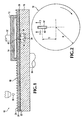
- a LAT 40 is formed in the overlying polishing pad 18 and aligned with the optical aperture 34 in the platen.
- the LAT 40 and aperture 34 can be positioned such that they have a view of the workpiece or substrate 14 held by the polishing head 12 during at least a portion of the platen's rotation, regardless of the translational position of the head 12.
- the light source 36 projects a light beam through the aperture 34 and the LAT 40 to impinge the surface of the overlying substrate 14 at least during a time when the LAT 40 is adjacent to the workpiece or substrate 14. Light reflected from the substrate forms a resultant beam that is detected by the detector 38.
- the light source and the detector are coupled to a computer (not shown) that receives the measured light intensity from the detector and uses it to determine the polishing endpoint, e.g., by detecting a sudden change in the reflectivity of the substrate that indicates the exposure of a new layer, by calculating the thickness removed from the outer layer (such as a transparent oxide layer) using interferometric principles, or by monitoring the signal for predetermined endpoint criteria.
- a computer not shown
- LAT delamination during polishing is LAT delamination during polishing.
- the lateral frictional force from the substrate during polishing can be greater than the forces holding the compression molding of the LAT to the sidewall of the opaque portion of the pad, thereby separating the LAT from the opaque portion.
- the present invention overcomes that problem by having a recessed LAT along with also having strong covalent bonding between the sidewalls of the LAT and the adjacent sidewalls of the opaque region of the pad.
- the LAT 40 is thin along the direction of the frictional force applied by the substrate during polishing (tangential to a radius in the case of a rotating a polishing pad) and wide in the direction perpendicular direction (along a radius in the case of a rotating a polishing pad).
- the LAT 40 can use an area about 0.5 inches wide and 2.0 inches long centered a distance D of about 7.5 inches (190.50 mm) from the center of the polishing pad 18 which has a radius of 15 inches.
- the LAT 40 can have an approximately rectangular shape with its longer dimension substantially parallel to the radius of the polishing pad that passes through the center of the LAT 40.
- the LAT 40 is surrounded by a plateau plane 42, e.g., the plateau plane is preferably about 5 to about 50 mils wide and surrounds the whole perimeter of the rectangular LAT.
- This plateau plane has several advantages associated with it in the present pad. These advantages include ease of manufacturing and improved slurry flow over the surface of the LAT.
- the plateau plane provides extra room to allow the support member to be removed from the cured LAT after the compression molding step.
- the LAT 40 is not as deep as the thickness of the polishing layer 20, so that the top surface 52 of the LAT 40 is not coplanar with the polishing surface 24 while the bottom surface 54 of the LAT is coplanar with a bottom surface 22 of the polishing layer.
- the straight sidewall perimeter of the LAT 40 can be secured, e.g., chemically bonded, to the inner sidewall edges of opaque portions 60 of the polishing layer 20.
- the planar plane 42 is shown on both sides of the top LAT surface 52.
- the polishing pad 40 is generally thin, e.g., less than 0.200 inches (200 mils or 5.08 mm), more preferably, from 0.050 to 0.150 inches (from 50 to 150 mils or from 1.27 mm to 3.81 mm).
- the total thickness of the polishing layer 20, adhesive 28 and liner 44 can be about 0.140 inches.
- the polishing layer 20 may be about 0.130 inches thick, with the adhesive 28 and the liner 44 providing the remaining 0.1 inches.
- the grooves 26 may preferably be about one fourth to one half the depth of the polishing pad, e.g., roughly 0.015 to 0.050 inches (15 mils to 50 mils of from 0.381 mm to 1.27 mm).
- the thickness of the LAT is generally equal to the thickness of the polishing pad minus the depth of the grooves. If the pad thickness is about 0.200 inches and the groove depth is 0.050 inches, then the LAT thickness is about 0.150 inches. If the pad thickness is about 0.050 inch and the groove depth is 0.015 inches, then the LAT thickness is about 0.035 inches. If the pad thickness is about 0.130 inches and the groove depth is 0.035 inches, then the LAT thickness is about 0.095 inches.
- the polishing pad 18 can also include a release liner 44 that spans the adhesive layer 28 on the opaque bottom surface 22 (shown in FIGS 3 and 5 ) and the LAT bottom surface 54 of the polishing pad.
- the liner is generally incompressible and also generally a fluid-impermeable layer, for example, polyethylene teraphthalate (PET), e.g., MylarTM PET film.
- PET polyethylene teraphthalate
- the release liner is manually peeled from the polishing pad, and the polishing layer backside 20 is applied to the platen with the pressure sensitive adhesive 28.
- the polishing layer 20 is formed and the bottom surface of the polishing layer 20 is then covered with the pressure sensitive adhesive 28 and a liner layer 44, as shown by FIG. 4 .
- Grooves 26 are formed in-situ in the polishing layer 20 as part of a pad compression molding process before attachment of the pressure sensitive adhesive 28 and a liner layer 44.
- the effective portion of the polishing pad 18 can include a polishing layer 20 with a polishing surface 24 to contact the substrate and bottom surfaces 22 and 54 to secure it to the platen 16 by an adhesive 28.
- the polishing pad 18 is made of at least one opaque region and at least one local area transparency region.
- the opaque portion of the present LAT pad may be made by reacting a mixture containing urethane prepolymer, porogen, and filler with a curative to form an opaque buff-colored thermoset polyurethane or polyurea having a substantially uniform microcellular, closed cell structure.
- This opaque pad portion is not made from a plurality of polymeric materials and a mixture of polymeric materials is not formed by the above reaction. Instead, this opaque pad portion is made from non-polymeric urethane precursor that forms a single type of polyurethane polymer.
- Suitable opacifying fillers in the opaque portion of the pad besides providing opacity to certain regions of the pad, may also provide improved lubricating behavior between the polishing pad and the workpiece being polished.
- Urethane prepolymers are a preferred reactive chemistry for reaction injection molding to form the polishing layer of the polishing pad of this invention.
- Prepolymers are intended to mean any precursor to the final polymerized product, including oligomers and monomers. Many such prepolymers are well known and commercially available. Urethane prepolymers generally comprise reactive moieties at the ends of the prepolymer chains.
- Commercially available isocyanate prepolymers include di-isocyanate prepolymers and tri-isocyanate prepolymers. Examples of di-isocyanate prepolymers include toluene diisocyanate and methylene-diphenyl diisocyanate.
- the isocyanate prepolymer comprises an average isocyanate functionality of at least two (i.e., at least two isocyanate reactive moieties in the prepolymer molecule).
- Average isocyanate functionality greater than 4 is generally not preferred, since processing of the resulting polymerized product can become difficult, depending upon the molding equipment and process used.
- Polyether prepolymers are particularly preferred.
- urethane and urea prepolymers useful in making the opaque portion of the pad include 80%-20% mixture of 2,4 and 2,6 isomers of toluene diisocyanate; 75%-25% mixture of 2,4 and 2,6 isomers of toluene diisocyanate; toluene diisocyanate polyfunctional isocyanates; methylene-diphenyl diisocyanate; polyether based toluene diisocyanate prepolymer; and polyether polytetramethylene glycol-toluene diisocyanate, as well as other prepolymers disclosed in US Published Patent Application No.2006/0276109 .
- porogens useful in making the opaque portion of the pad include polymeric microspheres such as inorganic salts, sugars and water-soluble particles.
- polymeric microspheres include polyvinyl alcohols, pectin, polyvinyl pyrrolidone, hydroxyethylcellulose, methylcellulose, hydropropylmethylcellulose, carboxymethylcellulose, hydroxypropylcellulose, polyacrylic acids, polyacrylamides, polyethylene glycols, polyhydroxyetheracrylites, starches, maleic acid copolymers, polyethylene oxide, polyurethanes, cyclodextrin and combinations thereof.
- gas-filled expanded hollow microspheres that has been used as a porogen in adding porosity to CMP pads is pre-expanded gas-filled EXPANCEL acrylonitrile vinylidiene chloride microspheres available from Akzo Nobel of Sundsvall, Sweden.
- the preferred range of expanded hollow-polymeric microspheres' average diameters is from about 12 to about 80 .mu.m (microns). Note the diameter of the microspheres may be varied and different sizes or mixtures of different microspheres may be employed in the polymeric material if desired.
- Other porogens are disclosed in US Patent No. 6,648,733 and in US Published Patent Application No. 2006/0276109 .
- Additional ingredients such as chain extenders, polyols, light stabilizers, thermal stabilizers and the like may also be used to make the opaque portion.
- the opaque pad portion of the pad contains opaque filler and a porogen whereas the transparent LAT portion does not require any opaque filler or porogen materials. Also, opaque pad portion of the pad will not have any water-soluble particles dispersed in the water-insoluble polymeric matrix opaque material.
- the opaque region is uniformly hydrophobic in nature. Upon conditioning, those conditioned portions will become more hydrophilic so as to be wettable.
- the average pore size will be from about 10 microns to about 100 microns, more preferably, from about 12 microns to about 90 microns.
- the local area transparency insert will be made by reacting a urethane prepolymer with a curative.
- Urethane prepolymer and curatives listed above for making the opaque portion of the pad may be useful for making the LAT. Since it is desirable that the covalent bonding between the sidewalls of the LAT and the adjacent sidewalls of the opaque portion be as strong as possible, the use of the same prepolymer for the LAT and opaque portions may be preferred in some instances.
- the transparent LAT portion is not made from a plurality of polymeric materials and a mixture of polymeric materials is not made by the above reaction.
- the present LAT insert pad portions are made from a non-polymeric urethane precursor that forms a single type of polyurethane or polyurea polymer.
- the resulting polymer for the present LAT is not a non-ambering urethane elastomer or does not have a refractive index intentionally designed to match the index of refraction of any slurry material to be used in a CMP process.
- the LAT portion of the present pad does not contain a clarifying material that causes the LAT to be more transparent.
- the LAT of the present invention will have a uniform single index of refraction throughout its volume.
- water-soluble particles are not dispersed in this water-insoluble polymeric matrix LAT material.
- the present LAT is not made of gas-permeable material or glass or crystalline material; silicone, poly(heptafluorobutacrylate) or poly(trifluorovinylacetate); or an acrylic-urethane oligomer or an acrylic-epoxy material.
- the present pad does not use any abrasive particles in either the LAT portion or the opaque portion.
- the LAT insert will have no pores and thus will have no intrinsic ability to absorb or transfer slurry particles.
- the opaque portion of the pad will have pores and thus will have the intrinsic ability to absorb or transfer slurry and slurry particles.
- Each pad will preferably have only one LAT; having more than one LAT in a pad is not preferred.
- a LAT that tilts from its top surface to its bottom surface i.e. does not have vertical side walls) is not contemplated.
- One preferred LAT is a 4-sided substantially rectangular cross-sectional shape (i.e. a 2 inch by 0.5 inch rectangle with radiused corners in the horizontal plane )(i.e. along the x,y-axis). However, other shapes may be contemplated in the future. In all vertical planes (i.e. along the z-axis), the LAT will have a vertical rectangular cross-sectional shape. In other words, each of the side walls of the LAT insert will be completely vertical. This facilitates the easy insertion of the LAT into the compression molding apparatus before molding. In contrast, the LAT inert will not be made of multiple sized sections such as a top hat design.
- the sidewall surfaces of the LAT in a pad are not contemplated to be an uneven side surface such as a serrated shape, a wavy shape and a toothed shape.
- a tilting LAT from its top surface to its bottom surface is not contemplated. Such shaped would complicate the insertion of the LAT in to the compression molding apparatus.
- LAT inserts are made by first adding the above-noted LAT insert prepolymer precursor ingredient (except for the curative) together in blend tank equipped with a mechanical stirrer, nitrogen gas head space a vacuum degassing system. The mixture after being thoroughly blended is transferred to a small mold via a mixing head where the curative is added to the mixture. A support member is then attached to the uncured LAT mixture. The transferred mixture is partially cured at a temperature for about 80 to 150 degrees C for 1 to 20 minutes in the small mold to make a non-liquid, non-fully cured transparent gel-like plug or article of the desired LAT insert shape supported on the support member. The insert is partially cured solely by thermal energy, and not by photocuring or other technique. As shown in FIG.
- a support member 62 that includes an epoxy holding block 46 with an adhesive layer on opposite ends (50 and 56) along with a polyimide film 48 attached to adhesive layer 50 are positioned in this small LAT mold before this partial curing step to support the LAT when it is placed in the larger pad mold.
- One surface of the polyimide film 48 becomes attached to the top surface 52 of the LAT during this partial curing step.
- the adhesive layer 56 on the other side of epoxy holding block is attached to a surface in the compression mold apparatus to hold the LAT/support member assembly in place during the molding operation.
- This gel-like LAT and support member insert is then placed in an area in the CMP LAT pad making apparatus (e.g. a compressive molding apparatus) that is designed to accept and position the LAT gel and support member.
- the CMP LAT pad making apparatus e.g. a compressive molding apparatus
- the process of the present invention does not contemplate using a polymeric sleeve to hold the gel insert in the mold.
- the LAT insert is positioned in the pad mold so that the top of the transparent LAT insert is below the top of the polishing surface (or top of the groove area) in the mold. It is not contemplated to have the opaque portion of the present pad extend over either the top or bottom surfaces of the present LAT insert.
- the LAT portion of the present pad is a non-compressible solid when fully cured.
- the gel-like LAT portion After being put in place and co-cured with the opaque portion, it is no longer a gel-like material that can be compressed nor is it an inorganic/organic hybrid sol-gel material.
- the relative wear rate of the LAT portion is immaterial because the location of the upper surface of the LAT is below the polishing surface and thus it is not subject to wear. Since the gel-like LAT and support member insert is made in a small mold and added to the pad mold a sufficient amount of time before the opaque liquid is added to the mold, the gel-like LAT and support member insert will cool below its quench temperature. In other words, it is not hot when added to the pad mold.
- the liquid opaque pad polymeric precursor mixture is separately made by blending the above-noted ingredients (except the curative) in a blend tank equipped with a mechanical stirrer and nitrogen gas head space. The mixture after being thoroughly mixed is transferred to a day tank. When ready for use, the mixture is transferred to the CMP LAT pad mold via a mixing head where the curative is added. The opaque precursor mix is added into the mold to fill up the rest of the mold and generally surround the LAT insert.
- One suitable mixing apparatus used in this operation is called a Baule mixing system.
- the compression mold Before adding the gel-like LAT and support member insert and the opaque portion, the compression mold is preheated to about 110 to 135 degrees C. After the insert is positioned in the mold and opaque portion fills the rest of the mold, the mold is closed and heated for about 8 to 15 minutes to partially cure the opaque material and further cure the transparent material.
- the compressive force in the compression molding apparatus may range from about 1000 pounds to 30000 pounds force or higher. Because the thermal mass of the top and bottom portions of the mold make it impractical to cycle the mold temperature during the production of the LAT pad, the inside of the mold stays at about the same processing temperature consistently while production is going on.
- LAT insert is made in a small mold and added to the pad mold a sufficient amount of time before the opaque liquid is added so that the LAT insert cools below its quench temperature.
- LAT/support member insert is not preheated up to the molding temperature prior to adding to the pad mold.
- the sidewalls of the LAT start to become covalently bonded to the adjacent sidewalls of the opaque portion of the pad, thus forming a strong pad where the LAT and opaque regions are strongly bound together.
- This covalent bonding is much stronger than either the bonding between previously cured LATs and uncured opaque area or previously cured opaque area with uncured LATs as suggested in the prior art references.
- the plateau sidewall and groove areas are also formed in-situ during this compression molding step.
- the plateau plane surrounding the top opening (and thus the top surface of the resulting LAT) has a width of about 5 mils to about 50 mils.
- Compression molding is a method of molding in which the molding material is placed in an open heated mold cavity. The mold is closed with a top force or plug member and pressure is applied to force the molding material into contact with all internal mold areas. Heat and pressure is maintained until the molding material has been sufficiently cured so that the resulting pad can be easily removed from the mold apparatus (i.e. demolded).
- the partially cured material which is a solid is "demolded" and removed from the mold.
- the support member is also removed from the top surface of the LAT.
- the plateau plane surrounding the top surface of the LAT allows for the easy removal of the support member from the LAT.
- the now exposed top surface of the LAT is a smooth surface positioned between the top polishing surface and the bottom surface of the polishing pad.
- the top surface of the LAT insert will not have a pattern or grooves designed into it. Only the top surface of the opaque portion of the pad will have the groove design in it.
- the LAT edges will not merge with sidewalls of the groove area, but will be positioned a short distance away from it.
- the polishing surface of the present pad is an opaque grooved polishing surface. Transparent grooves are not contemplated for this LAT pad.
- the solid partially cured pad is then preferably moved to a curing oven and heated for 8 to 24 hours at about 80 to 110 degrees C to complete the curing of both the LAT and opaque portions of the pad.
- This oven curing is not required if it is desired to complete the pad curing in the compression molding apparatus.
- the straight sidewalls of the LAT are chemically bonded directly by this thermal heating to the surrounding opaque area.
- the LAT will have a clear structurally distinct boundary with opaque portions of the pad, will be fixed in place in the pad and will not move independently of the opaque portion of the pad. No intermediate adhesive layer is needed between the LAT sidewalls and the surrounding opaque region.
- the resulting chemical bonding is stronger than when a completely cured LAT and uncured opaque material are heated together or when an uncured LAT and a completely cured opaque area are heated together.
- the present invention does not form a hole or aperture in cured opaque pad and then fill that hole or aperture with a transparent LAT insert. Instead, an opaque pad is molded around a preformed partially cured transparent gel-like article to form the LAT-containing polishing pad. Also, ultrasonic welding to attach the LAT to the opaque portion of the pad is not contemplated.
- the cured pad is removed from the oven and then the back side of the pad and the LAT insert is machined (the front or grooved side needed not be treated at all) so that the bottom surface of the opaque portion of the pad is flush with the bottom surface of the LAT. Also, the machining causes the desired pad thickness to be achieved.
- the smooth bottom surface of the LAT is modified by the machining so that the bottom surface of the cured thermoset polyurethane or polyurea local area transparency material is co-planar with the bottom surface of the opaque portions of the pad.
- the bottom surfaces of both the opaque portion and the LAT insert of the present pad do not have a designed pattern. Moreover, these bottom surfaces will have a uniform surface across the whole bottom of the LAT.
- the perimeter portion of the bottom surface will not be rougher than the center portion.
- the hardness of the opaque region of the pad is from about 25 to about 75 Shore D
- the hardness of the LAT is from about 25 to about75 Shore D
- the density of the opaque region of the pad is from about 0.6 to 1.2 grams per cubic centimeter
- the density of the LAT is from about 1 to about 1.2 grams per cubic centimeter.
- a “transfer adhesive film” is then placed over the bottom surface of the cured and machined pad.
- This "transfer adhesive film” is simply a roll of a pressure sensitive adhesive layer adhered to a release liner. It is unrolled and the adhesive layer is then adhered to the bottom surface of the LAT pad. The release liner is left in contact with that adhesive layer. Thus, a composite of the pad/adhesive layer/release layer is created.
- the transfer adhesive film is positioned and cut so that both the adhesive and the release liner cover the overall bottom surface of the pad.
- the release liner is preferably a layer of MYLAR polyethylene teraphthalate film that is preferably about 0.5 to 5 mils thick. Alternatively, paper release liner up to 10 mils thick may be used.
- the pressure sensitive adhesive positioned between the bottom surface of the polishing pad and the release liner is a releasable-bond type adhesive that is either an acrylic or rubber type having transparency properties suitable for this intended use.
- the bottom surface of the LAT will be flush with the bottom surface of the opaque pad material so that the PET film will form a flat sheet across the total bottom surface of the pad.
- the PET release liner will not have any holes or openings in it.
- This composite is then cleaned, inspected and packed for shipment to the end-user.
- the end-user when ready to use the pad, removes the release liner from the composite, exposing the adhesive layer. The end-user then positions the remainder of the composite against the CMP machine platen with the exposed adhesive layer adhering to the platen. The end-user disposes of the removed release liner after removal. A subpad is not contemplated being using below the release liner.
- the polishing pad of the invention is particularly suited for use in conjunction with a chemical-mechanical polishing (CMP) apparatus.
- the apparatus comprises a platen, which, when in use, is in motion and has a velocity that results from orbital, linear, or circular motion, a polishing pad of the invention in contact with the platen and moving with the platen when in motion, and a carrier that holds a workpiece to be polished by contacting and moving relative to the surface of the polishing pad.
- the polishing of the workpiece takes place by the workpiece being placed in contact with the polishing pad and then the polishing pad moving relative to the workpiece, typically with a polishing composition there between, so as to abrade at least a portion of the workpiece to polish the workpiece.
- the polishing composition typically comprises a liquid carrier (e.g., an aqueous carrier), a pH adjustor, and optionally an abrasive.
- the polishing composition optionally may further comprise oxidizing agents, organic acids, complexing agents, pH buffers, surfactants, corrosion inhibitors, anti-foaming agents, and the like.
- the CMP apparatus can be any suitable CMP apparatus, many of which are known in the art.
- the polishing pad of the invention also can be used with linear polishing tools.
- the CMP apparatus further comprises an in situ polishing endpoint detection system, many of which are known in the art.
- Techniques for inspecting and monitoring the polishing process by analyzing light or other radiation reflected from a surface of the workpiece are known in the art. Such methods are described, for example, in U.S. Pat. No. 5,196,353 , U.S. Pat. No. 5,433,651 , U.S. Pat. No. 5,609,511 , U.S. Pat. No. 5,643,046 , U.S. Pat. No. 5,658,183 , U.S. Pat. No. 5,730,642 , U.S. Pat. No. 5,838,447 , U.S. Pat. No.
- the inspection or monitoring of the progress of the polishing process with respect to a workpiece being polished enables the determination of the polishing end-point, i.e., the determination of when to terminate the polishing process with respect to a particular workpiece.
- the polishing pad of the invention is suitable for use in a method of polishing many types of workpieces (e.g., substrates or wafers) and workpiece materials.
- the polishing pads can be used to polish workpieces including memory storage devices, glass substrates, memory or rigid disks, metals (e.g., noble metals), magnetic heads, inter-layer dielectric (ILD) layers, polymeric films, low and high dielectric constant films, ferroelectrics, micro-electro-mechanical systems (MEMS), semiconductor wafers, field emission displays, and other microelectronic substrates, especially microelectronic substrates comprising insulating layers (e.g., metal oxide, silicon nitride, or low dielectric materials) and/or metal-containing layers (e.g., copper, tantalum, tungsten, aluminum, nickel, titanium, platinum, ruthenium, rhodium, iridium, alloys thereof, and mixtures thereof).
- insulating layers e.g., metal oxide, silicon
- memory or rigid disk refers to any magnetic disk, hard disk, rigid disk, or memory disk for retaining information in electromagnetic form.
- Memory or rigid disks typically have a surface that comprises nickel-phosphorus, but the surface can comprise any other suitable material.
- Suitable metal oxide insulating layers include, for example, alumina, silica, titania, ceria, zirconia, germania, magnesia, and combinations thereof.
- the workpiece can comprise, consist essentially of, or consist of any suitable metal composite.
- Suitable metal composites include, for example, metal nitrides (e.g., tantalum nitride, titanium nitride, and tungsten nitride), metal carbides (e.g., silicon carbide and tungsten carbide), nickel-phosphorus, alumino-borosilicate, borosilicate glass, phosphosilicate glass (PSG), borophosphosilicate glass (BPSG), silicon/germanium alloys, and silicon/germanium/carbon alloys.
- the workpiece also can comprise, consist essentially of, or consist of any suitable semiconductor base material. Suitable semiconductor base materials include single-crystal silicon, polycrystalline silicon, amorphous silicon, silicon-on-insulator, and gallium arsenide.
- the substrate can be, for example, a product substrate (e.g., which includes multiple memory or processor dies), a test substrate, a bare substrate, and a gating substrate.
- the substrate can be at various stages of integrated circuit fabrication, e.g., the substrate can be a bare wafer, or it can include one or more deposited and/or patterned layers.
- the term substrate can include circular disks and rectangular sheets.
- an anti-scattering layer positioned over the top or bottom surfaces of the present LAT is not contemplated.
- No electronic or mechanical sensing means or measuring devices located within either the LAT portion or the opaque portion of the pad are contemplated for the present polishing pad.
- the LAT in the present pad will not have an anti-fouling treatment on the top or bottom surfaces to prevent slurry material from sticking to those surfaces and hindering the endpoint detection.
- the top and bottom surfaces of the present LAT will not be treated with a corona treatment, flame treatment or fluorine gas treatment.
- the release liner will be attached to the LAT and opaque portions of the pad by a single adhesive layer.
- a combination of 2 different adhesives between that release liner and the present LAT pad or using no-adhesive means to adhere the release liner to the bottom pad surface is not contemplated. Also, using an epoxy resin adhesive to adhere the pad to the PET film is not contemplated.
- the present pad does not have an intermediate material between the LAT sidewalls and the adjacent opaque sidewalls and will not have any porous fibrous matrix in either the LAT insert portion or the opaque portion. Adding magnetic particles to the release liner of the present LAT pad is not contemplated. It is not contemplated to use laser ablation to remove surface roughness in the lower surface of the LAT insert and/or forming micro-lens by said laser ablation.
- the present co-curing does not employ a two-stage cooling process during pad molding to first allow a LAT region of the pad to form by fast cooling and then allow the opaque region to form by slow cooling.
Landscapes
- Engineering & Computer Science (AREA)
- Mechanical Engineering (AREA)
- Mechanical Treatment Of Semiconductor (AREA)
- Finish Polishing, Edge Sharpening, And Grinding By Specific Grinding Devices (AREA)
Applications Claiming Priority (2)
| Application Number | Priority Date | Filing Date | Title |
|---|---|---|---|
| US12/657,135 US9017140B2 (en) | 2010-01-13 | 2010-01-13 | CMP pad with local area transparency |
| PCT/US2011/020870 WO2011088057A1 (en) | 2010-01-13 | 2011-01-11 | Cmp pad with local area transparency |
Publications (2)
| Publication Number | Publication Date |
|---|---|
| EP2523777A1 EP2523777A1 (en) | 2012-11-21 |
| EP2523777B1 true EP2523777B1 (en) | 2015-12-02 |
Family
ID=43896755
Family Applications (1)
| Application Number | Title | Priority Date | Filing Date |
|---|---|---|---|
| EP11700493.7A Active EP2523777B1 (en) | 2010-01-13 | 2011-01-11 | Cmp pad with local area transparency |
Country Status (10)
Families Citing this family (62)
| Publication number | Priority date | Publication date | Assignee | Title |
|---|---|---|---|---|
| US9156124B2 (en) * | 2010-07-08 | 2015-10-13 | Nexplanar Corporation | Soft polishing pad for polishing a semiconductor substrate |
| US8628384B2 (en) * | 2010-09-30 | 2014-01-14 | Nexplanar Corporation | Polishing pad for eddy current end-point detection |
| US8657653B2 (en) | 2010-09-30 | 2014-02-25 | Nexplanar Corporation | Homogeneous polishing pad for eddy current end-point detection |
| US8535115B2 (en) * | 2011-01-28 | 2013-09-17 | Applied Materials, Inc. | Gathering spectra from multiple optical heads |
| US8920219B2 (en) * | 2011-07-15 | 2014-12-30 | Nexplanar Corporation | Polishing pad with alignment aperture |
| US20130205679A1 (en) * | 2012-02-14 | 2013-08-15 | Innopad, Inc. | Method of manufacturing a chemical mechanical planarization pad |
| US8986585B2 (en) * | 2012-03-22 | 2015-03-24 | Rohm And Haas Electronic Materials Cmp Holdings, Inc. | Method of manufacturing chemical mechanical polishing layers having a window |
| US9156125B2 (en) | 2012-04-11 | 2015-10-13 | Cabot Microelectronics Corporation | Polishing pad with light-stable light-transmitting region |
| US20140120802A1 (en) * | 2012-10-31 | 2014-05-01 | Wayne O. Duescher | Abrasive platen wafer surface optical monitoring system |
| US9649742B2 (en) | 2013-01-22 | 2017-05-16 | Nexplanar Corporation | Polishing pad having polishing surface with continuous protrusions |
| US10160092B2 (en) * | 2013-03-14 | 2018-12-25 | Cabot Microelectronics Corporation | Polishing pad having polishing surface with continuous protrusions having tapered sidewalls |
| US9259820B2 (en) * | 2014-03-28 | 2016-02-16 | Rohm And Haas Electronic Materials Cmp Holdings, Inc. | Chemical mechanical polishing pad with polishing layer and window |
| US9216489B2 (en) * | 2014-03-28 | 2015-12-22 | Rohm And Haas Electronic Materials Cmp Holdings, Inc. | Chemical mechanical polishing pad with endpoint detection window |
| US9238294B2 (en) * | 2014-06-18 | 2016-01-19 | Nexplanar Corporation | Polishing pad having porogens with liquid filler |
| US9873180B2 (en) | 2014-10-17 | 2018-01-23 | Applied Materials, Inc. | CMP pad construction with composite material properties using additive manufacturing processes |
| US10875145B2 (en) | 2014-10-17 | 2020-12-29 | Applied Materials, Inc. | Polishing pads produced by an additive manufacturing process |
| US10821573B2 (en) | 2014-10-17 | 2020-11-03 | Applied Materials, Inc. | Polishing pads produced by an additive manufacturing process |
| US9776361B2 (en) | 2014-10-17 | 2017-10-03 | Applied Materials, Inc. | Polishing articles and integrated system and methods for manufacturing chemical mechanical polishing articles |
| US11745302B2 (en) | 2014-10-17 | 2023-09-05 | Applied Materials, Inc. | Methods and precursor formulations for forming advanced polishing pads by use of an additive manufacturing process |
| KR102295988B1 (ko) | 2014-10-17 | 2021-09-01 | 어플라이드 머티어리얼스, 인코포레이티드 | 애디티브 제조 프로세스들을 이용한 복합 재료 특성들을 갖는 cmp 패드 구성 |
| US10875153B2 (en) | 2014-10-17 | 2020-12-29 | Applied Materials, Inc. | Advanced polishing pad materials and formulations |
| US10399201B2 (en) | 2014-10-17 | 2019-09-03 | Applied Materials, Inc. | Advanced polishing pads having compositional gradients by use of an additive manufacturing process |
| US20160144477A1 (en) * | 2014-11-21 | 2016-05-26 | Diane Scott | Coated compressive subpad for chemical mechanical polishing |
| US10946495B2 (en) * | 2015-01-30 | 2021-03-16 | Cmc Materials, Inc. | Low density polishing pad |
| US9475168B2 (en) * | 2015-03-26 | 2016-10-25 | Rohm And Haas Electronic Materials Cmp Holdings, Inc. | Polishing pad window |
| TWI695752B (zh) * | 2015-10-16 | 2020-06-11 | 美商應用材料股份有限公司 | 用於以積層製程形成先進拋光墊的配方 |
| KR20230169424A (ko) | 2015-10-30 | 2023-12-15 | 어플라이드 머티어리얼스, 인코포레이티드 | 원하는 제타 전위를 가진 연마 제품을 형성하는 장치 및 방법 |
| US10593574B2 (en) | 2015-11-06 | 2020-03-17 | Applied Materials, Inc. | Techniques for combining CMP process tracking data with 3D printed CMP consumables |
| US10391605B2 (en) | 2016-01-19 | 2019-08-27 | Applied Materials, Inc. | Method and apparatus for forming porous advanced polishing pads using an additive manufacturing process |
| CN113146464A (zh) | 2016-01-19 | 2021-07-23 | 应用材料公司 | 多孔化学机械抛光垫 |
| US10213894B2 (en) * | 2016-02-26 | 2019-02-26 | Applied Materials, Inc. | Method of placing window in thin polishing pad |
| TWI593511B (zh) | 2016-06-08 | 2017-08-01 | 智勝科技股份有限公司 | 研磨墊及研磨方法 |
| JP2019528187A (ja) | 2016-08-31 | 2019-10-10 | アプライド マテリアルズ インコーポレイテッドApplied Materials,Incorporated | 環状プラテン又は研磨パッドを有する研磨システム |
| US10786885B2 (en) * | 2017-01-20 | 2020-09-29 | Applied Materials, Inc. | Thin plastic polishing article for CMP applications |
| US20180265989A1 (en) * | 2017-03-17 | 2018-09-20 | Toshiba Memory Corporation | Substrate treatment apparatus and substrate treatment method |
| JP6360586B1 (ja) * | 2017-04-13 | 2018-07-18 | 三菱電線工業株式会社 | Cmp装置のウエハ保持用の弾性膜 |
| US20180304539A1 (en) | 2017-04-21 | 2018-10-25 | Applied Materials, Inc. | Energy delivery system with array of energy sources for an additive manufacturing apparatus |
| KR101966809B1 (ko) * | 2017-05-18 | 2019-08-13 | 세메스 주식회사 | 기판 연마 장치 및 기판 연마 방법 |
| KR20200014364A (ko) * | 2017-06-01 | 2020-02-10 | 도쿄엘렉트론가부시키가이샤 | 게터링층 형성 장치, 게터링층 형성 방법 및 컴퓨터 기억 매체 |
| US11471999B2 (en) | 2017-07-26 | 2022-10-18 | Applied Materials, Inc. | Integrated abrasive polishing pads and manufacturing methods |
| US11072050B2 (en) * | 2017-08-04 | 2021-07-27 | Applied Materials, Inc. | Polishing pad with window and manufacturing methods thereof |
| WO2019032286A1 (en) | 2017-08-07 | 2019-02-14 | Applied Materials, Inc. | ABRASIVE DISTRIBUTION POLISHING PADS AND METHODS OF MAKING SAME |
| JP6948878B2 (ja) * | 2017-08-22 | 2021-10-13 | ラピスセミコンダクタ株式会社 | 半導体製造装置及び半導体基板の研磨方法 |
| US10636761B2 (en) * | 2017-08-29 | 2020-04-28 | Electronics And Telecommunications Reearch Institute | Method of fabricating a semiconductor package |
| US11192215B2 (en) * | 2017-11-16 | 2021-12-07 | Rohm And Haas Electronic Materials Cmp Holdings, Inc. | Polishing pad with pad wear indicator |
| US10465097B2 (en) * | 2017-11-16 | 2019-11-05 | Rohm And Haas Electronic Materials Cmp Holdings, Inc. | Aliphatic UV cured polyurethane optical endpoint detection windows with high UV transparency for CMP polishing pads |
| US11325221B2 (en) * | 2017-11-16 | 2022-05-10 | Rohm And Haas Electronic Materials Cmp Holdings, Inc. | Polishing pad with multipurpose composite window |
| US11826876B2 (en) | 2018-05-07 | 2023-11-28 | Applied Materials, Inc. | Hydrophilic and zeta potential tunable chemical mechanical polishing pads |
| KR20210042171A (ko) | 2018-09-04 | 2021-04-16 | 어플라이드 머티어리얼스, 인코포레이티드 | 진보한 폴리싱 패드들을 위한 제형들 |
| US12138735B2 (en) * | 2018-11-28 | 2024-11-12 | Taiwan Semiconductor Manufacturing Co., Ltd. | Multi-layered windows for use in chemical-mechanical planarization systems |
| KR102674027B1 (ko) | 2019-01-29 | 2024-06-12 | 삼성전자주식회사 | 재생 연마패드 |
| US11851570B2 (en) | 2019-04-12 | 2023-12-26 | Applied Materials, Inc. | Anionic polishing pads formed by printing processes |
| US11813712B2 (en) | 2019-12-20 | 2023-11-14 | Applied Materials, Inc. | Polishing pads having selectively arranged porosity |
| KR102142236B1 (ko) * | 2020-01-10 | 2020-08-06 | (주)제이쓰리 | 초평탄화 형상제어 웨이퍼 가공장치 |
| TW202204461A (zh) * | 2020-03-31 | 2022-02-01 | 日商德山股份有限公司 | Cmp研磨墊用中空微球 |
| US11806829B2 (en) | 2020-06-19 | 2023-11-07 | Applied Materials, Inc. | Advanced polishing pads and related polishing pad manufacturing methods |
| EP4281249A4 (en) * | 2021-01-25 | 2024-12-25 | CMC Materials LLC | REGULAR TEXTURE SURFACE LIMIT POINT WINDOW |
| US11878389B2 (en) | 2021-02-10 | 2024-01-23 | Applied Materials, Inc. | Structures formed using an additive manufacturing process for regenerating surface texture in situ |
| KR20230152728A (ko) * | 2021-03-03 | 2023-11-03 | 어플라이드 머티어리얼스, 인코포레이티드 | 화학적 기계적 연마를 위한 음향 모니터링 및 센서들 |
| CN115122232B (zh) * | 2021-03-29 | 2024-08-20 | 万华化学集团电子材料有限公司 | 一种微孔聚氨酯抛光垫的制备方法、抛光垫及其应用 |
| KR102624629B1 (ko) * | 2021-11-19 | 2024-01-15 | 에스케이하이닉스 주식회사 | 윈도우 삽입형 연마패드 및 이의 제조방법 |
| JP7696822B2 (ja) * | 2021-12-28 | 2025-06-23 | 株式会社荏原製作所 | 研磨装置および研磨方法 |
Family Cites Families (139)
| Publication number | Priority date | Publication date | Assignee | Title |
|---|---|---|---|---|
| US5196353A (en) | 1992-01-03 | 1993-03-23 | Micron Technology, Inc. | Method for controlling a semiconductor (CMP) process by measuring a surface temperature and developing a thermal image of the wafer |
| US6614529B1 (en) | 1992-12-28 | 2003-09-02 | Applied Materials, Inc. | In-situ real-time monitoring technique and apparatus for endpoint detection of thin films during chemical/mechanical polishing planarization |
| US5658183A (en) | 1993-08-25 | 1997-08-19 | Micron Technology, Inc. | System for real-time control of semiconductor wafer polishing including optical monitoring |
| US5433651A (en) * | 1993-12-22 | 1995-07-18 | International Business Machines Corporation | In-situ endpoint detection and process monitoring method and apparatus for chemical-mechanical polishing |
| JP3270282B2 (ja) | 1994-02-21 | 2002-04-02 | 株式会社東芝 | 半導体製造装置及び半導体装置の製造方法 |
| JP3313505B2 (ja) | 1994-04-14 | 2002-08-12 | 株式会社日立製作所 | 研磨加工法 |
| US6876454B1 (en) | 1995-03-28 | 2005-04-05 | Applied Materials, Inc. | Apparatus and method for in-situ endpoint detection for chemical mechanical polishing operations |
| US6676717B1 (en) | 1995-03-28 | 2004-01-13 | Applied Materials Inc | Apparatus and method for in-situ endpoint detection for chemical mechanical polishing operations |
| US5893796A (en) | 1995-03-28 | 1999-04-13 | Applied Materials, Inc. | Forming a transparent window in a polishing pad for a chemical mechanical polishing apparatus |
| US6719818B1 (en) | 1995-03-28 | 2004-04-13 | Applied Materials, Inc. | Apparatus and method for in-situ endpoint detection for chemical mechanical polishing operations |
| US5964643A (en) | 1995-03-28 | 1999-10-12 | Applied Materials, Inc. | Apparatus and method for in-situ monitoring of chemical mechanical polishing operations |
| US6537133B1 (en) | 1995-03-28 | 2003-03-25 | Applied Materials, Inc. | Method for in-situ endpoint detection for chemical mechanical polishing operations |
| US5838447A (en) | 1995-07-20 | 1998-11-17 | Ebara Corporation | Polishing apparatus including thickness or flatness detector |
| US5605760A (en) | 1995-08-21 | 1997-02-25 | Rodel, Inc. | Polishing pads |
| US5738574A (en) | 1995-10-27 | 1998-04-14 | Applied Materials, Inc. | Continuous processing system for chemical mechanical polishing |
| US5609517A (en) | 1995-11-20 | 1997-03-11 | International Business Machines Corporation | Composite polishing pad |
| US5733176A (en) | 1996-05-24 | 1998-03-31 | Micron Technology, Inc. | Polishing pad and method of use |
| US5872633A (en) | 1996-07-26 | 1999-02-16 | Speedfam Corporation | Methods and apparatus for detecting removal of thin film layers during planarization |
| US6648733B2 (en) | 1997-04-04 | 2003-11-18 | Rodel Holdings, Inc. | Polishing pads and methods relating thereto |
| US6068539A (en) | 1998-03-10 | 2000-05-30 | Lam Research Corporation | Wafer polishing device with movable window |
| US20040082271A1 (en) | 1999-01-25 | 2004-04-29 | Wiswesser Andreas Norbert | Polishing pad with window |
| US6994607B2 (en) | 2001-12-28 | 2006-02-07 | Applied Materials, Inc. | Polishing pad with window |
| US6716085B2 (en) | 2001-12-28 | 2004-04-06 | Applied Materials Inc. | Polishing pad with transparent window |
| US6832950B2 (en) | 2002-10-28 | 2004-12-21 | Applied Materials, Inc. | Polishing pad with window |
| KR100435246B1 (ko) | 1999-03-31 | 2004-06-11 | 가부시키가이샤 니콘 | 연마체, 연마장치, 연마장치의 조정방법, 연마막 두께또는 연마종점의 측정방법, 및 반도체 디바이스의 제조방법 |
| US6146242A (en) | 1999-06-11 | 2000-11-14 | Strasbaugh, Inc. | Optical view port for chemical mechanical planarization endpoint detection |
| US6171181B1 (en) | 1999-08-17 | 2001-01-09 | Rodel Holdings, Inc. | Molded polishing pad having integral window |
| JP3867844B2 (ja) | 1999-08-27 | 2007-01-17 | 旭化成エレクトロニクス株式会社 | 研磨パッドおよび研磨装置 |
| US6454630B1 (en) | 1999-09-14 | 2002-09-24 | Applied Materials, Inc. | Rotatable platen having a transparent window for a chemical mechanical polishing apparatus and method of making the same |
| US6524164B1 (en) | 1999-09-14 | 2003-02-25 | Applied Materials, Inc. | Polishing pad with transparent window having reduced window leakage for a chemical mechanical polishing apparatus |
| WO2001023141A1 (en) | 1999-09-29 | 2001-04-05 | Rodel Holdings, Inc. | Polishing pad |
| US6726528B2 (en) | 2002-05-14 | 2004-04-27 | Strasbaugh | Polishing pad with optical sensor |
| JP2003524300A (ja) | 2000-02-25 | 2003-08-12 | ロデール ホールディングス インコーポレイテッド | 透明部分のある研磨パッド |
| KR100789663B1 (ko) | 2000-03-15 | 2007-12-31 | 롬 앤드 하스 일렉트로닉 머티리얼스 씨엠피 홀딩스 인코포레이티드 | 연마층에 투명 윈도우 부분을 갖는 연마 패드 |
| US8485862B2 (en) | 2000-05-19 | 2013-07-16 | Applied Materials, Inc. | Polishing pad for endpoint detection and related methods |
| US6685537B1 (en) | 2000-06-05 | 2004-02-03 | Speedfam-Ipec Corporation | Polishing pad window for a chemical mechanical polishing tool |
| US6612901B1 (en) | 2000-06-07 | 2003-09-02 | Micron Technology, Inc. | Apparatus for in-situ optical endpointing of web-format planarizing machines in mechanical or chemical-mechanical planarization of microelectronic-device substrate assemblies |
| US6485354B1 (en) | 2000-06-09 | 2002-11-26 | Strasbaugh | Polishing pad with built-in optical sensor |
| US6428386B1 (en) | 2000-06-16 | 2002-08-06 | Micron Technology, Inc. | Planarizing pads, planarizing machines, and methods for mechanical and/or chemical-mechanical planarization of microelectronic-device substrate assemblies |
| JP2002001647A (ja) * | 2000-06-19 | 2002-01-08 | Rodel Nitta Co | 研磨パッド |
| ATE496730T1 (de) | 2000-09-29 | 2011-02-15 | Strasbaugh Inc | Polierkissen mit eingebautem optischem sensor |
| JP2004511108A (ja) | 2000-10-06 | 2004-04-08 | キャボット マイクロエレクトロニクス コーポレイション | 充填材入り透光性領域を含む研磨パッド |
| US20020072296A1 (en) | 2000-11-29 | 2002-06-13 | Muilenburg Michael J. | Abrasive article having a window system for polishing wafers, and methods |
| US6623331B2 (en) | 2001-02-16 | 2003-09-23 | Cabot Microelectronics Corporation | Polishing disk with end-point detection port |
| US6840843B2 (en) | 2001-03-01 | 2005-01-11 | Cabot Microelectronics Corporation | Method for manufacturing a polishing pad having a compressed translucent region |
| US20020137431A1 (en) | 2001-03-23 | 2002-09-26 | Labunsky Michael A. | Methods and apparatus for polishing and planarization |
| US6641470B1 (en) | 2001-03-30 | 2003-11-04 | Lam Research Corporation | Apparatus for accurate endpoint detection in supported polishing pads |
| DE60228784D1 (de) | 2001-04-25 | 2008-10-23 | Jsr Corp | Lichtduchlässiges Polierkissen für eine Halbleiterschleife |
| JP4131632B2 (ja) | 2001-06-15 | 2008-08-13 | 株式会社荏原製作所 | ポリッシング装置及び研磨パッド |
| JP4570286B2 (ja) | 2001-07-03 | 2010-10-27 | ニッタ・ハース株式会社 | 研磨パッド |
| JP2003133270A (ja) | 2001-10-26 | 2003-05-09 | Jsr Corp | 化学機械研磨用窓材及び研磨パッド |
| US6722249B2 (en) | 2001-11-06 | 2004-04-20 | Rodel Holdings, Inc | Method of fabricating a polishing pad having an optical window |
| US6702866B2 (en) | 2002-01-10 | 2004-03-09 | Speedfam-Ipec Corporation | Homogeneous fixed abrasive polishing pad |
| US6884146B2 (en) | 2002-02-04 | 2005-04-26 | Kla-Tencor Technologies Corp. | Systems and methods for characterizing a polishing process |
| US7001242B2 (en) | 2002-02-06 | 2006-02-21 | Applied Materials, Inc. | Method and apparatus of eddy current monitoring for chemical mechanical polishing |
| US6875077B2 (en) | 2002-03-18 | 2005-04-05 | Raytech Innovative Solutions, Inc. | Polishing pad for use in chemical/mechanical planarization of semiconductor wafers having a transparent window for end-point determination and method of making |
| US6524176B1 (en) | 2002-03-25 | 2003-02-25 | Macronix International Co. Ltd. | Polishing pad |
| US20030207661A1 (en) * | 2002-05-01 | 2003-11-06 | Alexander Tregub | Annealing of CMP polishing pads |
| US6752690B1 (en) * | 2002-06-12 | 2004-06-22 | Clinton O. Fruitman | Method of making polishing pad for planarization of semiconductor wafers |
| KR20050059123A (ko) | 2002-08-30 | 2005-06-17 | 도레이 가부시끼가이샤 | 연마 패드, 정반 홀 커버 및 연마장치 및 연마방법 및 반도체 디바이스의 제조방법 |
| US20070010169A1 (en) | 2002-09-25 | 2007-01-11 | Ppg Industries Ohio, Inc. | Polishing pad with window for planarization |
| WO2004028744A1 (en) | 2002-09-25 | 2004-04-08 | Ppg Industries Ohio, Inc. | Polishing pad with window for planarization |
| US7435165B2 (en) | 2002-10-28 | 2008-10-14 | Cabot Microelectronics Corporation | Transparent microporous materials for CMP |
| US7267607B2 (en) | 2002-10-28 | 2007-09-11 | Cabot Microelectronics Corporation | Transparent microporous materials for CMP |
| TWI220405B (en) | 2002-11-19 | 2004-08-21 | Iv Technologies Co Ltd | Method of fabricating a polishing pad having a detection window thereon |
| KR101047933B1 (ko) | 2002-11-27 | 2011-07-11 | 도요 고무 고교 가부시키가이샤 | 연마 패드 및 반도체 장치의 제조 방법 |
| US6806100B1 (en) | 2002-12-24 | 2004-10-19 | Lam Research Corporation | Molded end point detection window for chemical mechanical planarization |
| US6676483B1 (en) | 2003-02-03 | 2004-01-13 | Rodel Holdings, Inc. | Anti-scattering layer for polishing pad windows |
| US6960120B2 (en) | 2003-02-10 | 2005-11-01 | Cabot Microelectronics Corporation | CMP pad with composite transparent window |
| US6832947B2 (en) * | 2003-02-10 | 2004-12-21 | Cabot Microelectronics Corporation | CMP pad with composite transparent window |
| TW200530378A (en) | 2003-03-11 | 2005-09-16 | Toyo Tire & Rubber Co | Polishing pad and semiconductor device manufacturing method |
| US7704125B2 (en) * | 2003-03-24 | 2010-04-27 | Nexplanar Corporation | Customized polishing pads for CMP and methods of fabrication and use thereof |
| US7377840B2 (en) | 2004-07-21 | 2008-05-27 | Neopad Technologies Corporation | Methods for producing in-situ grooves in chemical mechanical planarization (CMP) pads, and novel CMP pad designs |
| US8864859B2 (en) | 2003-03-25 | 2014-10-21 | Nexplanar Corporation | Customized polishing pads for CMP and methods of fabrication and use thereof |
| CA2519942A1 (en) | 2003-03-25 | 2004-10-14 | Neopad Technologies Corporation | Chip customized polish pads for chemical mechanical planarization (cmp) |
| EP1466699A1 (en) | 2003-04-09 | 2004-10-13 | JSR Corporation | Abrasive pad, method and metal mold for manufacturing the same, and semiconductor wafer polishing method |
| US7238097B2 (en) | 2003-04-11 | 2007-07-03 | Nihon Microcoating Co., Ltd. | Polishing pad and method of producing same |
| US20040209066A1 (en) | 2003-04-17 | 2004-10-21 | Swisher Robert G. | Polishing pad with window for planarization |
| US20040224611A1 (en) | 2003-04-22 | 2004-11-11 | Jsr Corporation | Polishing pad and method of polishing a semiconductor wafer |
| KR100532440B1 (ko) | 2003-06-05 | 2005-11-30 | 삼성전자주식회사 | 윈도로의 유체의 침투를 막는 실링 장벽부를 가지는 화학기계적 연마 장비에 사용되는 연마 패드 |
| KR100541545B1 (ko) | 2003-06-16 | 2006-01-11 | 삼성전자주식회사 | 화학기계적 연마 장비의 연마 테이블 |
| US6884156B2 (en) | 2003-06-17 | 2005-04-26 | Cabot Microelectronics Corporation | Multi-layer polishing pad material for CMP |
| US6997777B2 (en) | 2003-06-17 | 2006-02-14 | Cabot Microelectronics Corporation | Ultrasonic welding method for the manufacture of a polishing pad comprising an optically transmissive region |
| KR100526877B1 (ko) | 2003-06-23 | 2005-11-09 | 삼성전자주식회사 | 반도체 웨이퍼용 cmp 설비의 폴리싱 패드 |
| US7183213B2 (en) | 2003-07-17 | 2007-02-27 | Jsr Corporation | Chemical mechanical polishing pad and chemical mechanical polishing method |
| US7195539B2 (en) | 2003-09-19 | 2007-03-27 | Cabot Microelectronics Coporation | Polishing pad with recessed window |
| US7264536B2 (en) | 2003-09-23 | 2007-09-04 | Applied Materials, Inc. | Polishing pad with window |
| US20050173259A1 (en) | 2004-02-06 | 2005-08-11 | Applied Materials, Inc. | Endpoint system for electro-chemical mechanical polishing |
| US8066552B2 (en) | 2003-10-03 | 2011-11-29 | Applied Materials, Inc. | Multi-layer polishing pad for low-pressure polishing |
| US7258602B2 (en) | 2003-10-22 | 2007-08-21 | Iv Technologies Co., Ltd. | Polishing pad having grooved window therein and method of forming the same |
| KR101152747B1 (ko) | 2003-10-31 | 2012-06-18 | 어플라이드 머티어리얼스, 인코포레이티드 | 마찰 센서를 이용한 폴리싱 종료점 탐지 시스템 및 방법 |
| US6984163B2 (en) | 2003-11-25 | 2006-01-10 | Rohm And Haas Electronic Materials Cmp Holdings, Inc. | Polishing pad with high optical transmission window |
| US7132033B2 (en) | 2004-02-27 | 2006-11-07 | Rohm And Haas Electronic Materials Cmp Holdings, Inc. | Method of forming a layered polishing pad |
| USD559064S1 (en) | 2004-03-17 | 2008-01-08 | Jsr Corporation | Polishing pad |
| USD559063S1 (en) | 2004-03-17 | 2008-01-08 | Jsr Corporation | Polishing pad |
| US7204742B2 (en) | 2004-03-25 | 2007-04-17 | Cabot Microelectronics Corporation | Polishing pad comprising hydrophobic region and endpoint detection port |
| US6986705B2 (en) | 2004-04-05 | 2006-01-17 | Rimpad Tech Ltd. | Polishing pad and method of making same |
| CN2841246Y (zh) * | 2004-04-21 | 2006-11-29 | 应用材料股份有限公司 | 研磨垫 |
| CN100424830C (zh) | 2004-04-23 | 2008-10-08 | Jsr株式会社 | 用于抛光半导体晶片的抛光垫、层叠体和方法 |
| US20050245171A1 (en) | 2004-04-28 | 2005-11-03 | Jsr Corporation | Chemical mechanical polishing pad, manufacturing process thereof and chemical mechanical polishing method for semiconductor wafers |
| US7354334B1 (en) | 2004-05-07 | 2008-04-08 | Applied Materials, Inc. | Reducing polishing pad deformation |
| US7018581B2 (en) * | 2004-06-10 | 2006-03-28 | Rohm And Haas Electronic Materials Cmp Holdings, Inc. | Method of forming a polishing pad with reduced stress window |
| US7252871B2 (en) | 2004-06-16 | 2007-08-07 | Rohm And Haas Electronic Materials Cmp Holdings, Inc. | Polishing pad having a pressure relief channel |
| US7182670B2 (en) | 2004-09-22 | 2007-02-27 | Rohm And Haas Electronic Materials Cmp Holdings, Inc. | CMP pad having a streamlined windowpane |
| USD559648S1 (en) | 2004-10-05 | 2008-01-15 | Jsr Corporation | Polishing pad |
| USD560457S1 (en) | 2004-10-05 | 2008-01-29 | Jsr Corporation | Polishing pad |
| USD559065S1 (en) | 2004-10-05 | 2008-01-08 | Jsr Corporation | Polishing pad |
| US20060089094A1 (en) | 2004-10-27 | 2006-04-27 | Swisher Robert G | Polyurethane urea polishing pad |
| US20060089095A1 (en) | 2004-10-27 | 2006-04-27 | Swisher Robert G | Polyurethane urea polishing pad |
| KR100953928B1 (ko) | 2004-12-10 | 2010-04-23 | 도요 고무 고교 가부시키가이샤 | 연마 패드 및 연마 패드의 제조 방법 |
| TWI385050B (zh) | 2005-02-18 | 2013-02-11 | Nexplanar Corp | 用於cmp之特製拋光墊及其製造方法及其用途 |
| WO2006089293A1 (en) | 2005-02-18 | 2006-08-24 | Neopad Technologies Corporation | Customized polishing pads for cmp and methods of fabrication and use thereof |
| US7179159B2 (en) | 2005-05-02 | 2007-02-20 | Applied Materials, Inc. | Materials for chemical mechanical polishing |
| US20060291530A1 (en) | 2005-06-23 | 2006-12-28 | Alexander Tregub | Treatment of CMP pad window to improve transmittance |
| US20070049169A1 (en) | 2005-08-02 | 2007-03-01 | Vaidya Neha P | Nonwoven polishing pads for chemical mechanical polishing |
| US20070037487A1 (en) | 2005-08-10 | 2007-02-15 | Kuo Charles C | Polishing pad having a sealed pressure relief channel |
| US7169017B1 (en) | 2005-08-10 | 2007-01-30 | Rohm And Haas Electronic Materials Cmp Holdings, Inc. | Polishing pad having a window with reduced surface roughness |
| TW200709892A (en) | 2005-08-18 | 2007-03-16 | Rohm & Haas Elect Mat | Transparent polishing pad |
| US7764377B2 (en) | 2005-08-22 | 2010-07-27 | Applied Materials, Inc. | Spectrum based endpointing for chemical mechanical polishing |
| US7210980B2 (en) | 2005-08-26 | 2007-05-01 | Applied Materials, Inc. | Sealed polishing pad, system and methods |
| TWI288048B (en) | 2005-10-20 | 2007-10-11 | Iv Technologies Co Ltd | A polishing pad and producing method thereof |
| US20070197134A1 (en) | 2006-02-15 | 2007-08-23 | Applied Materials, Inc. | Polishing article with integrated window stripe |
| US7621798B1 (en) | 2006-03-07 | 2009-11-24 | Applied Materials, Inc. | Reducing polishing pad deformation |
| US7179151B1 (en) | 2006-03-27 | 2007-02-20 | Freescale Semiconductor, Inc. | Polishing pad, a polishing apparatus, and a process for using the polishing pad |
| US7497763B2 (en) | 2006-03-27 | 2009-03-03 | Freescale Semiconductor, Inc. | Polishing pad, a polishing apparatus, and a process for using the polishing pad |
| JP2007260827A (ja) * | 2006-03-28 | 2007-10-11 | Toyo Tire & Rubber Co Ltd | 研磨パッドの製造方法 |
| JP2007307639A (ja) * | 2006-05-17 | 2007-11-29 | Toyo Tire & Rubber Co Ltd | 研磨パッド |
| JP5110677B2 (ja) | 2006-05-17 | 2012-12-26 | 東洋ゴム工業株式会社 | 研磨パッド |
| US7942724B2 (en) * | 2006-07-03 | 2011-05-17 | Applied Materials, Inc. | Polishing pad with window having multiple portions |
| JP2008100331A (ja) * | 2006-10-20 | 2008-05-01 | Toyo Tire & Rubber Co Ltd | 長尺研磨パッドの製造方法 |
| JP2008226911A (ja) * | 2007-03-08 | 2008-09-25 | Jsr Corp | 化学機械研磨用パッド、化学機械研磨用積層体パッド、および化学機械研磨方法 |
| JP5363470B2 (ja) | 2007-06-08 | 2013-12-11 | アプライド マテリアルズ インコーポレイテッド | 窓付きの薄い研磨パッド及び成形プロセス |
| US7455571B1 (en) | 2007-06-20 | 2008-11-25 | Rohm And Haas Electronic Materials Cmp Holdings, Inc. | Window polishing pad |
| WO2009070352A1 (en) | 2007-11-30 | 2009-06-04 | Innopad, Inc. | Chemical-mechanical planarization pad having end point detection window |
| JP2009224384A (ja) | 2008-03-13 | 2009-10-01 | Toyo Tire & Rubber Co Ltd | 研磨パッド及び半導体デバイスの製造方法 |
| US9180570B2 (en) | 2008-03-14 | 2015-11-10 | Nexplanar Corporation | Grooved CMP pad |
| JP5385377B2 (ja) | 2008-05-15 | 2014-01-08 | スリーエム イノベイティブ プロパティズ カンパニー | 終点窓を持った研磨パッドおよびこれを用いたシステムおよび使用方法 |
| US20090305610A1 (en) | 2008-06-06 | 2009-12-10 | Applied Materials, Inc. | Multiple window pad assembly |
| US7967661B2 (en) | 2008-06-19 | 2011-06-28 | Micron Technology, Inc. | Systems and pads for planarizing microelectronic workpieces and associated methods of use and manufacture |
-
2010
- 2010-01-13 US US12/657,135 patent/US9017140B2/en active Active
-
2011
- 2011-01-11 SG SG10201408738RA patent/SG10201408738RA/en unknown
- 2011-01-11 EP EP11700493.7A patent/EP2523777B1/en active Active
- 2011-01-11 MY MYPI2012003162A patent/MY165538A/en unknown
- 2011-01-11 CN CN201180005898.6A patent/CN102770239B/zh active Active
- 2011-01-11 KR KR1020127019401A patent/KR101495145B1/ko active Active
- 2011-01-11 JP JP2012549005A patent/JP5503019B2/ja active Active
- 2011-01-11 SG SG2012049086A patent/SG182327A1/en unknown
- 2011-01-11 WO PCT/US2011/020870 patent/WO2011088057A1/en active Application Filing
- 2011-01-13 TW TW100101301A patent/TWI490083B/zh active
-
2012
- 2012-06-26 IL IL220649A patent/IL220649A/en active IP Right Grant
-
2013
- 2013-12-17 JP JP2013259788A patent/JP5820869B2/ja active Active
-
2015
- 2015-01-20 JP JP2015008413A patent/JP2015096293A/ja active Pending
Also Published As
| Publication number | Publication date |
|---|---|
| WO2011088057A1 (en) | 2011-07-21 |
| MY165538A (en) | 2018-04-03 |
| TWI490083B (zh) | 2015-07-01 |
| JP5503019B2 (ja) | 2014-05-28 |
| JP2013517146A (ja) | 2013-05-16 |
| CN102770239A (zh) | 2012-11-07 |
| EP2523777A1 (en) | 2012-11-21 |
| CN102770239B (zh) | 2016-04-20 |
| TW201143985A (en) | 2011-12-16 |
| KR20120135210A (ko) | 2012-12-12 |
| JP5820869B2 (ja) | 2015-11-24 |
| IL220649A0 (en) | 2012-08-30 |
| US9017140B2 (en) | 2015-04-28 |
| US20110171883A1 (en) | 2011-07-14 |
| IL220649A (en) | 2016-10-31 |
| SG10201408738RA (en) | 2015-02-27 |
| JP2014050959A (ja) | 2014-03-20 |
| KR101495145B1 (ko) | 2015-02-24 |
| JP2015096293A (ja) | 2015-05-21 |
| SG182327A1 (en) | 2012-08-30 |
Similar Documents
| Publication | Publication Date | Title |
|---|---|---|
| EP2523777B1 (en) | Cmp pad with local area transparency | |
| US9597769B2 (en) | Polishing pad with polishing surface layer having an aperture or opening above a transparent foundation layer | |
| US9931728B2 (en) | Polishing pad with foundation layer and polishing surface layer | |
| EP2785496B1 (en) | Polishing pad with foundation layer and polishing surface layer | |
| US9931729B2 (en) | Polishing pad with grooved foundation layer and polishing surface layer | |
| KR101633745B1 (ko) | 연마 패드 | |
| CN100349267C (zh) | 研磨垫及半导体器件的制造方法 | |
| JP4744087B2 (ja) | 研磨パッド及び半導体デバイスの製造方法 | |
| JP4890744B2 (ja) | 研磨パッドおよび半導体デバイスの製造方法 | |
| JP2006128563A (ja) | 半導体ウエハ研磨用研磨パッドおよび半導体デバイスの製造方法 | |
| JP2006187837A (ja) | 研磨パッド |
Legal Events
| Date | Code | Title | Description |
|---|---|---|---|
| PUAI | Public reference made under article 153(3) epc to a published international application that has entered the european phase |
Free format text: ORIGINAL CODE: 0009012 |
|
| 17P | Request for examination filed |
Effective date: 20120803 |
|
| AK | Designated contracting states |
Kind code of ref document: A1 Designated state(s): AL AT BE BG CH CY CZ DE DK EE ES FI FR GB GR HR HU IE IS IT LI LT LU LV MC MK MT NL NO PL PT RO RS SE SI SK SM TR |
|
| RIN1 | Information on inventor provided before grant (corrected) |
Inventor name: HUANG, PING Inventor name: SCOTT, DIANE Inventor name: FRENTZEL, RICHARD Inventor name: ALLISON, WILLIAM Inventor name: KERPRICH, ROBERT |
|
| DAX | Request for extension of the european patent (deleted) | ||
| 17Q | First examination report despatched |
Effective date: 20131218 |
|
| GRAP | Despatch of communication of intention to grant a patent |
Free format text: ORIGINAL CODE: EPIDOSNIGR1 |
|
| INTG | Intention to grant announced |
Effective date: 20150612 |
|
| RIN1 | Information on inventor provided before grant (corrected) |
Inventor name: SCOTT, DIANE Inventor name: KERPRICH, ROBERT Inventor name: ALLISON, WILLIAM Inventor name: HUANG, PING Inventor name: FRENTZEL, RICHARD |
|
| GRAS | Grant fee paid |
Free format text: ORIGINAL CODE: EPIDOSNIGR3 |
|
| GRAA | (expected) grant |
Free format text: ORIGINAL CODE: 0009210 |
|
| AK | Designated contracting states |
Kind code of ref document: B1 Designated state(s): AL AT BE BG CH CY CZ DE DK EE ES FI FR GB GR HR HU IE IS IT LI LT LU LV MC MK MT NL NO PL PT RO RS SE SI SK SM TR |
|
| REG | Reference to a national code |
Ref country code: GB Ref legal event code: FG4D |
|
| REG | Reference to a national code |
Ref country code: AT Ref legal event code: REF Ref document number: 763407 Country of ref document: AT Kind code of ref document: T Effective date: 20151215 Ref country code: CH Ref legal event code: EP |
|
| REG | Reference to a national code |
Ref country code: IE Ref legal event code: FG4D |
|
| REG | Reference to a national code |
Ref country code: DE Ref legal event code: R096 Ref document number: 602011021783 Country of ref document: DE |
|
| REG | Reference to a national code |
Ref country code: NL Ref legal event code: MP Effective date: 20160302 |
|
| REG | Reference to a national code |
Ref country code: LT Ref legal event code: MG4D |
|
| REG | Reference to a national code |
Ref country code: AT Ref legal event code: MK05 Ref document number: 763407 Country of ref document: AT Kind code of ref document: T Effective date: 20151202 |
|
| PG25 | Lapsed in a contracting state [announced via postgrant information from national office to epo] |
Ref country code: ES Free format text: LAPSE BECAUSE OF FAILURE TO SUBMIT A TRANSLATION OF THE DESCRIPTION OR TO PAY THE FEE WITHIN THE PRESCRIBED TIME-LIMIT Effective date: 20151202 Ref country code: LT Free format text: LAPSE BECAUSE OF FAILURE TO SUBMIT A TRANSLATION OF THE DESCRIPTION OR TO PAY THE FEE WITHIN THE PRESCRIBED TIME-LIMIT Effective date: 20151202 Ref country code: NO Free format text: LAPSE BECAUSE OF FAILURE TO SUBMIT A TRANSLATION OF THE DESCRIPTION OR TO PAY THE FEE WITHIN THE PRESCRIBED TIME-LIMIT Effective date: 20160302 |
|
| PG25 | Lapsed in a contracting state [announced via postgrant information from national office to epo] |
Ref country code: BE Free format text: LAPSE BECAUSE OF NON-PAYMENT OF DUE FEES Effective date: 20160131 Ref country code: FI Free format text: LAPSE BECAUSE OF FAILURE TO SUBMIT A TRANSLATION OF THE DESCRIPTION OR TO PAY THE FEE WITHIN THE PRESCRIBED TIME-LIMIT Effective date: 20151202 Ref country code: GR Free format text: LAPSE BECAUSE OF FAILURE TO SUBMIT A TRANSLATION OF THE DESCRIPTION OR TO PAY THE FEE WITHIN THE PRESCRIBED TIME-LIMIT Effective date: 20160303 Ref country code: PL Free format text: LAPSE BECAUSE OF FAILURE TO SUBMIT A TRANSLATION OF THE DESCRIPTION OR TO PAY THE FEE WITHIN THE PRESCRIBED TIME-LIMIT Effective date: 20151202 Ref country code: SE Free format text: LAPSE BECAUSE OF FAILURE TO SUBMIT A TRANSLATION OF THE DESCRIPTION OR TO PAY THE FEE WITHIN THE PRESCRIBED TIME-LIMIT Effective date: 20151202 Ref country code: RS Free format text: LAPSE BECAUSE OF FAILURE TO SUBMIT A TRANSLATION OF THE DESCRIPTION OR TO PAY THE FEE WITHIN THE PRESCRIBED TIME-LIMIT Effective date: 20151202 Ref country code: NL Free format text: LAPSE BECAUSE OF FAILURE TO SUBMIT A TRANSLATION OF THE DESCRIPTION OR TO PAY THE FEE WITHIN THE PRESCRIBED TIME-LIMIT Effective date: 20151202 Ref country code: LV Free format text: LAPSE BECAUSE OF FAILURE TO SUBMIT A TRANSLATION OF THE DESCRIPTION OR TO PAY THE FEE WITHIN THE PRESCRIBED TIME-LIMIT Effective date: 20151202 Ref country code: AT Free format text: LAPSE BECAUSE OF FAILURE TO SUBMIT A TRANSLATION OF THE DESCRIPTION OR TO PAY THE FEE WITHIN THE PRESCRIBED TIME-LIMIT Effective date: 20151202 |
|
| PG25 | Lapsed in a contracting state [announced via postgrant information from national office to epo] |
Ref country code: IS Free format text: LAPSE BECAUSE OF FAILURE TO SUBMIT A TRANSLATION OF THE DESCRIPTION OR TO PAY THE FEE WITHIN THE PRESCRIBED TIME-LIMIT Effective date: 20151202 |
|
| PG25 | Lapsed in a contracting state [announced via postgrant information from national office to epo] |
Ref country code: IT Free format text: LAPSE BECAUSE OF FAILURE TO SUBMIT A TRANSLATION OF THE DESCRIPTION OR TO PAY THE FEE WITHIN THE PRESCRIBED TIME-LIMIT Effective date: 20151202 Ref country code: CZ Free format text: LAPSE BECAUSE OF FAILURE TO SUBMIT A TRANSLATION OF THE DESCRIPTION OR TO PAY THE FEE WITHIN THE PRESCRIBED TIME-LIMIT Effective date: 20151202 |
|
| PG25 | Lapsed in a contracting state [announced via postgrant information from national office to epo] |
Ref country code: EE Free format text: LAPSE BECAUSE OF FAILURE TO SUBMIT A TRANSLATION OF THE DESCRIPTION OR TO PAY THE FEE WITHIN THE PRESCRIBED TIME-LIMIT Effective date: 20151202 Ref country code: SM Free format text: LAPSE BECAUSE OF FAILURE TO SUBMIT A TRANSLATION OF THE DESCRIPTION OR TO PAY THE FEE WITHIN THE PRESCRIBED TIME-LIMIT Effective date: 20151202 Ref country code: RO Free format text: LAPSE BECAUSE OF FAILURE TO SUBMIT A TRANSLATION OF THE DESCRIPTION OR TO PAY THE FEE WITHIN THE PRESCRIBED TIME-LIMIT Effective date: 20151202 Ref country code: IS Free format text: LAPSE BECAUSE OF FAILURE TO SUBMIT A TRANSLATION OF THE DESCRIPTION OR TO PAY THE FEE WITHIN THE PRESCRIBED TIME-LIMIT Effective date: 20160402 Ref country code: LU Free format text: LAPSE BECAUSE OF FAILURE TO SUBMIT A TRANSLATION OF THE DESCRIPTION OR TO PAY THE FEE WITHIN THE PRESCRIBED TIME-LIMIT Effective date: 20160111 Ref country code: PT Free format text: LAPSE BECAUSE OF FAILURE TO SUBMIT A TRANSLATION OF THE DESCRIPTION OR TO PAY THE FEE WITHIN THE PRESCRIBED TIME-LIMIT Effective date: 20160404 Ref country code: SK Free format text: LAPSE BECAUSE OF FAILURE TO SUBMIT A TRANSLATION OF THE DESCRIPTION OR TO PAY THE FEE WITHIN THE PRESCRIBED TIME-LIMIT Effective date: 20151202 |
|
| REG | Reference to a national code |
Ref country code: CH Ref legal event code: PL |
|
| REG | Reference to a national code |
Ref country code: DE Ref legal event code: R097 Ref document number: 602011021783 Country of ref document: DE |
|
| PG25 | Lapsed in a contracting state [announced via postgrant information from national office to epo] |
Ref country code: MC Free format text: LAPSE BECAUSE OF FAILURE TO SUBMIT A TRANSLATION OF THE DESCRIPTION OR TO PAY THE FEE WITHIN THE PRESCRIBED TIME-LIMIT Effective date: 20151202 |
|
| PLBE | No opposition filed within time limit |
Free format text: ORIGINAL CODE: 0009261 |
|
| STAA | Information on the status of an ep patent application or granted ep patent |
Free format text: STATUS: NO OPPOSITION FILED WITHIN TIME LIMIT |
|
| REG | Reference to a national code |
Ref country code: FR Ref legal event code: ST Effective date: 20160930 |
|
| PG25 | Lapsed in a contracting state [announced via postgrant information from national office to epo] |
Ref country code: CH Free format text: LAPSE BECAUSE OF NON-PAYMENT OF DUE FEES Effective date: 20160131 Ref country code: LI Free format text: LAPSE BECAUSE OF NON-PAYMENT OF DUE FEES Effective date: 20160131 Ref country code: DK Free format text: LAPSE BECAUSE OF FAILURE TO SUBMIT A TRANSLATION OF THE DESCRIPTION OR TO PAY THE FEE WITHIN THE PRESCRIBED TIME-LIMIT Effective date: 20151202 |
|
| 26N | No opposition filed |
Effective date: 20160905 |
|
| PG25 | Lapsed in a contracting state [announced via postgrant information from national office to epo] |
Ref country code: FR Free format text: LAPSE BECAUSE OF NON-PAYMENT OF DUE FEES Effective date: 20160202 Ref country code: SI Free format text: LAPSE BECAUSE OF FAILURE TO SUBMIT A TRANSLATION OF THE DESCRIPTION OR TO PAY THE FEE WITHIN THE PRESCRIBED TIME-LIMIT Effective date: 20151202 |
|
| PG25 | Lapsed in a contracting state [announced via postgrant information from national office to epo] |
Ref country code: BE Free format text: LAPSE BECAUSE OF FAILURE TO SUBMIT A TRANSLATION OF THE DESCRIPTION OR TO PAY THE FEE WITHIN THE PRESCRIBED TIME-LIMIT Effective date: 20151202 |
|
| PG25 | Lapsed in a contracting state [announced via postgrant information from national office to epo] |
Ref country code: MT Free format text: LAPSE BECAUSE OF FAILURE TO SUBMIT A TRANSLATION OF THE DESCRIPTION OR TO PAY THE FEE WITHIN THE PRESCRIBED TIME-LIMIT Effective date: 20151202 |
|
| REG | Reference to a national code |
Ref country code: DE Ref legal event code: R081 Ref document number: 602011021783 Country of ref document: DE Owner name: CMC MATERIALS, INC., AURORA, US Free format text: FORMER OWNER: NEXPLANAR CORP., HILLSBORO, OREG., US Ref country code: DE Ref legal event code: R082 Ref document number: 602011021783 Country of ref document: DE Representative=s name: LORENZ SEIDLER GOSSEL RECHTSANWAELTE PATENTANW, DE Ref country code: DE Ref legal event code: R081 Ref document number: 602011021783 Country of ref document: DE Owner name: CABOT MICROELECTRONICS CORP., AURORA, US Free format text: FORMER OWNER: NEXPLANAR CORP., HILLSBORO, OREG., US |
|
| REG | Reference to a national code |
Ref country code: GB Ref legal event code: 732E Free format text: REGISTERED BETWEEN 20171005 AND 20171011 |
|
| PG25 | Lapsed in a contracting state [announced via postgrant information from national office to epo] |
Ref country code: HU Free format text: LAPSE BECAUSE OF FAILURE TO SUBMIT A TRANSLATION OF THE DESCRIPTION OR TO PAY THE FEE WITHIN THE PRESCRIBED TIME-LIMIT; INVALID AB INITIO Effective date: 20110111 Ref country code: CY Free format text: LAPSE BECAUSE OF FAILURE TO SUBMIT A TRANSLATION OF THE DESCRIPTION OR TO PAY THE FEE WITHIN THE PRESCRIBED TIME-LIMIT Effective date: 20151202 |
|
| PG25 | Lapsed in a contracting state [announced via postgrant information from national office to epo] |
Ref country code: HR Free format text: LAPSE BECAUSE OF FAILURE TO SUBMIT A TRANSLATION OF THE DESCRIPTION OR TO PAY THE FEE WITHIN THE PRESCRIBED TIME-LIMIT Effective date: 20151202 Ref country code: MT Free format text: LAPSE BECAUSE OF FAILURE TO SUBMIT A TRANSLATION OF THE DESCRIPTION OR TO PAY THE FEE WITHIN THE PRESCRIBED TIME-LIMIT Effective date: 20160131 Ref country code: TR Free format text: LAPSE BECAUSE OF FAILURE TO SUBMIT A TRANSLATION OF THE DESCRIPTION OR TO PAY THE FEE WITHIN THE PRESCRIBED TIME-LIMIT Effective date: 20151202 Ref country code: MK Free format text: LAPSE BECAUSE OF FAILURE TO SUBMIT A TRANSLATION OF THE DESCRIPTION OR TO PAY THE FEE WITHIN THE PRESCRIBED TIME-LIMIT Effective date: 20151202 |
|
| PG25 | Lapsed in a contracting state [announced via postgrant information from national office to epo] |
Ref country code: BG Free format text: LAPSE BECAUSE OF FAILURE TO SUBMIT A TRANSLATION OF THE DESCRIPTION OR TO PAY THE FEE WITHIN THE PRESCRIBED TIME-LIMIT Effective date: 20151202 |
|
| PG25 | Lapsed in a contracting state [announced via postgrant information from national office to epo] |
Ref country code: AL Free format text: LAPSE BECAUSE OF FAILURE TO SUBMIT A TRANSLATION OF THE DESCRIPTION OR TO PAY THE FEE WITHIN THE PRESCRIBED TIME-LIMIT Effective date: 20151202 |
|
| REG | Reference to a national code |
Ref country code: DE Ref legal event code: R081 Ref document number: 602011021783 Country of ref document: DE Owner name: CMC MATERIALS, INC., AURORA, US Free format text: FORMER OWNER: CABOT MICROELECTRONICS CORP., AURORA, ILL., US Ref country code: DE Ref legal event code: R081 Ref document number: 602011021783 Country of ref document: DE Owner name: CMC MATERIALS LLC (N.D.GES.D.STAATES DELAWARE), US Free format text: FORMER OWNER: CABOT MICROELECTRONICS CORP., AURORA, ILL., US |
|
| P01 | Opt-out of the competence of the unified patent court (upc) registered |
Effective date: 20230530 |
|
| PGFP | Annual fee paid to national office [announced via postgrant information from national office to epo] |
Ref country code: GB Payment date: 20241219 Year of fee payment: 15 |
|
| PGFP | Annual fee paid to national office [announced via postgrant information from national office to epo] |
Ref country code: IE Payment date: 20241220 Year of fee payment: 15 |
|
| PGFP | Annual fee paid to national office [announced via postgrant information from national office to epo] |
Ref country code: DE Payment date: 20241218 Year of fee payment: 15 |
|
| REG | Reference to a national code |
Ref country code: DE Ref legal event code: R081 Ref document number: 602011021783 Country of ref document: DE Owner name: CMC MATERIALS LLC (N.D.GES.D.STAATES DELAWARE), US Free format text: FORMER OWNER: CMC MATERIALS, INC., AURORA, IL, US |