EP2519986B1 - Vergussmasse als diffusionsbarriere für wassermoleküle - Google Patents
Vergussmasse als diffusionsbarriere für wassermoleküle Download PDFInfo
- Publication number
- EP2519986B1 EP2519986B1 EP10784718.8A EP10784718A EP2519986B1 EP 2519986 B1 EP2519986 B1 EP 2519986B1 EP 10784718 A EP10784718 A EP 10784718A EP 2519986 B1 EP2519986 B1 EP 2519986B1
- Authority
- EP
- European Patent Office
- Prior art keywords
- glass
- particles
- silica particles
- epoxy resin
- silicone
- Prior art date
- Legal status (The legal status is an assumption and is not a legal conclusion. Google has not performed a legal analysis and makes no representation as to the accuracy of the status listed.)
- Not-in-force
Links
- 238000009792 diffusion process Methods 0.000 title claims description 20
- 230000004888 barrier function Effects 0.000 title claims description 18
- 150000001875 compounds Chemical class 0.000 title description 19
- 238000004382 potting Methods 0.000 title description 17
- XLYOFNOQVPJJNP-UHFFFAOYSA-N water Substances O XLYOFNOQVPJJNP-UHFFFAOYSA-N 0.000 title description 12
- 239000002245 particle Substances 0.000 claims description 50
- VYPSYNLAJGMNEJ-UHFFFAOYSA-N Silicium dioxide Chemical compound O=[Si]=O VYPSYNLAJGMNEJ-UHFFFAOYSA-N 0.000 claims description 48
- OAICVXFJPJFONN-UHFFFAOYSA-N Phosphorus Chemical compound [P] OAICVXFJPJFONN-UHFFFAOYSA-N 0.000 claims description 41
- 239000011521 glass Substances 0.000 claims description 38
- 229920000647 polyepoxide Polymers 0.000 claims description 29
- 229920002050 silicone resin Polymers 0.000 claims description 29
- 239000003822 epoxy resin Substances 0.000 claims description 26
- 239000000203 mixture Substances 0.000 claims description 26
- 239000011248 coating agent Substances 0.000 claims description 17
- 238000000576 coating method Methods 0.000 claims description 17
- 238000000034 method Methods 0.000 claims description 11
- 238000004519 manufacturing process Methods 0.000 claims description 9
- 229910052605 nesosilicate Inorganic materials 0.000 claims description 8
- 229910052688 Gadolinium Inorganic materials 0.000 claims description 6
- 229910052788 barium Inorganic materials 0.000 claims description 6
- 230000008569 process Effects 0.000 claims description 6
- 229910052712 strontium Inorganic materials 0.000 claims description 6
- 229910052684 Cerium Inorganic materials 0.000 claims description 5
- 150000004762 orthosilicates Chemical class 0.000 claims description 5
- 229910052765 Lutetium Inorganic materials 0.000 claims description 4
- 229910052771 Terbium Inorganic materials 0.000 claims description 4
- 229910052791 calcium Inorganic materials 0.000 claims description 4
- 229910052727 yttrium Inorganic materials 0.000 claims description 4
- 229910052782 aluminium Inorganic materials 0.000 claims description 3
- 150000003961 organosilicon compounds Chemical class 0.000 claims description 3
- 229910052693 Europium Inorganic materials 0.000 claims description 2
- 229910052772 Samarium Inorganic materials 0.000 claims description 2
- 239000012190 activator Substances 0.000 claims description 2
- 229910052804 chromium Inorganic materials 0.000 claims description 2
- 229910052733 gallium Inorganic materials 0.000 claims description 2
- 150000002500 ions Chemical class 0.000 claims description 2
- 229910052748 manganese Inorganic materials 0.000 claims description 2
- 238000002156 mixing Methods 0.000 claims description 2
- 150000004767 nitrides Chemical class 0.000 claims description 2
- 229910052706 scandium Inorganic materials 0.000 claims description 2
- LSGOVYNHVSXFFJ-UHFFFAOYSA-N vanadate(3-) Chemical class [O-][V]([O-])([O-])=O LSGOVYNHVSXFFJ-UHFFFAOYSA-N 0.000 claims description 2
- 229910052784 alkaline earth metal Inorganic materials 0.000 claims 3
- 239000005084 Strontium aluminate Substances 0.000 claims 2
- 229910052909 inorganic silicate Inorganic materials 0.000 claims 1
- 229920005989 resin Polymers 0.000 description 14
- 239000011347 resin Substances 0.000 description 14
- 239000000725 suspension Substances 0.000 description 12
- 239000011159 matrix material Substances 0.000 description 8
- 239000000377 silicon dioxide Substances 0.000 description 8
- 230000008878 coupling Effects 0.000 description 7
- 238000010168 coupling process Methods 0.000 description 7
- 238000005859 coupling reaction Methods 0.000 description 7
- 239000008367 deionised water Substances 0.000 description 6
- 238000001035 drying Methods 0.000 description 6
- 238000003756 stirring Methods 0.000 description 6
- 239000004593 Epoxy Substances 0.000 description 5
- BPQQTUXANYXVAA-UHFFFAOYSA-N Orthosilicate Chemical compound [O-][Si]([O-])([O-])[O-] BPQQTUXANYXVAA-UHFFFAOYSA-N 0.000 description 5
- -1 oxy- Chemical class 0.000 description 5
- 150000004756 silanes Chemical class 0.000 description 5
- 239000000463 material Substances 0.000 description 4
- 229920001296 polysiloxane Polymers 0.000 description 4
- 229910021641 deionized water Inorganic materials 0.000 description 3
- 230000004907 flux Effects 0.000 description 3
- 238000005259 measurement Methods 0.000 description 3
- 239000000843 powder Substances 0.000 description 3
- 150000003839 salts Chemical class 0.000 description 3
- 238000002444 silanisation Methods 0.000 description 3
- 239000000243 solution Substances 0.000 description 3
- 238000003860 storage Methods 0.000 description 3
- 239000000126 substance Substances 0.000 description 3
- 239000013008 thixotropic agent Substances 0.000 description 3
- XDLMVUHYZWKMMD-UHFFFAOYSA-N 3-trimethoxysilylpropyl 2-methylprop-2-enoate Chemical compound CO[Si](OC)(OC)CCCOC(=O)C(C)=C XDLMVUHYZWKMMD-UHFFFAOYSA-N 0.000 description 2
- 239000006057 Non-nutritive feed additive Substances 0.000 description 2
- XUIMIQQOPSSXEZ-UHFFFAOYSA-N Silicon Chemical compound [Si] XUIMIQQOPSSXEZ-UHFFFAOYSA-N 0.000 description 2
- 238000000354 decomposition reaction Methods 0.000 description 2
- 230000007423 decrease Effects 0.000 description 2
- 238000009826 distribution Methods 0.000 description 2
- 230000000694 effects Effects 0.000 description 2
- FWDBOZPQNFPOLF-UHFFFAOYSA-N ethenyl(triethoxy)silane Chemical compound CCO[Si](OCC)(OCC)C=C FWDBOZPQNFPOLF-UHFFFAOYSA-N 0.000 description 2
- 239000007788 liquid Substances 0.000 description 2
- 239000000049 pigment Substances 0.000 description 2
- 229920000642 polymer Polymers 0.000 description 2
- 239000007858 starting material Substances 0.000 description 2
- DQZNLOXENNXVAD-UHFFFAOYSA-N trimethoxy-[2-(7-oxabicyclo[4.1.0]heptan-4-yl)ethyl]silane Chemical compound C1C(CC[Si](OC)(OC)OC)CCC2OC21 DQZNLOXENNXVAD-UHFFFAOYSA-N 0.000 description 2
- 238000007740 vapor deposition Methods 0.000 description 2
- BVKZGUZCCUSVTD-UHFFFAOYSA-M Bicarbonate Chemical class OC([O-])=O BVKZGUZCCUSVTD-UHFFFAOYSA-M 0.000 description 1
- 229910004261 CaF 2 Inorganic materials 0.000 description 1
- VEXZGXHMUGYJMC-UHFFFAOYSA-M Chloride anion Chemical compound [Cl-] VEXZGXHMUGYJMC-UHFFFAOYSA-M 0.000 description 1
- 229910002601 GaN Inorganic materials 0.000 description 1
- JMASRVWKEDWRBT-UHFFFAOYSA-N Gallium nitride Chemical compound [Ga]#N JMASRVWKEDWRBT-UHFFFAOYSA-N 0.000 description 1
- 229910002651 NO3 Inorganic materials 0.000 description 1
- NHNBFGGVMKEFGY-UHFFFAOYSA-N Nitrate Chemical compound [O-][N+]([O-])=O NHNBFGGVMKEFGY-UHFFFAOYSA-N 0.000 description 1
- 229910019142 PO4 Inorganic materials 0.000 description 1
- ZLMJMSJWJFRBEC-UHFFFAOYSA-N Potassium Chemical compound [K] ZLMJMSJWJFRBEC-UHFFFAOYSA-N 0.000 description 1
- 229910004283 SiO 4 Inorganic materials 0.000 description 1
- 229910003668 SrAl Inorganic materials 0.000 description 1
- 150000001242 acetic acid derivatives Chemical class 0.000 description 1
- 239000002318 adhesion promoter Substances 0.000 description 1
- 230000002411 adverse Effects 0.000 description 1
- 238000005054 agglomeration Methods 0.000 description 1
- 230000002776 aggregation Effects 0.000 description 1
- 229910052783 alkali metal Inorganic materials 0.000 description 1
- AUCDRFABNLOFRE-UHFFFAOYSA-N alumane;indium Chemical compound [AlH3].[In] AUCDRFABNLOFRE-UHFFFAOYSA-N 0.000 description 1
- XAGFODPZIPBFFR-UHFFFAOYSA-N aluminium Chemical compound [Al] XAGFODPZIPBFFR-UHFFFAOYSA-N 0.000 description 1
- 238000000149 argon plasma sintering Methods 0.000 description 1
- DSAJWYNOEDNPEQ-UHFFFAOYSA-N barium atom Chemical compound [Ba] DSAJWYNOEDNPEQ-UHFFFAOYSA-N 0.000 description 1
- 239000002585 base Substances 0.000 description 1
- 230000000903 blocking effect Effects 0.000 description 1
- 239000007767 bonding agent Substances 0.000 description 1
- 150000004649 carbonic acid derivatives Chemical class 0.000 description 1
- 150000007942 carboxylates Chemical class 0.000 description 1
- 238000005266 casting Methods 0.000 description 1
- ZMIGMASIKSOYAM-UHFFFAOYSA-N cerium Chemical compound [Ce][Ce][Ce][Ce][Ce][Ce][Ce][Ce][Ce][Ce][Ce][Ce][Ce][Ce][Ce][Ce][Ce][Ce][Ce][Ce][Ce][Ce][Ce][Ce][Ce][Ce][Ce][Ce][Ce][Ce][Ce][Ce][Ce][Ce][Ce][Ce][Ce][Ce] ZMIGMASIKSOYAM-UHFFFAOYSA-N 0.000 description 1
- 239000003795 chemical substances by application Substances 0.000 description 1
- 238000010276 construction Methods 0.000 description 1
- 230000001419 dependent effect Effects 0.000 description 1
- 238000011161 development Methods 0.000 description 1
- 230000018109 developmental process Effects 0.000 description 1
- 239000002019 doping agent Substances 0.000 description 1
- LYCAIKOWRPUZTN-UHFFFAOYSA-N ethylene glycol Natural products OCCO LYCAIKOWRPUZTN-UHFFFAOYSA-N 0.000 description 1
- 238000009472 formulation Methods 0.000 description 1
- 229910021485 fumed silica Inorganic materials 0.000 description 1
- 125000000524 functional group Chemical group 0.000 description 1
- UIWYJDYFSGRHKR-UHFFFAOYSA-N gadolinium atom Chemical compound [Gd] UIWYJDYFSGRHKR-UHFFFAOYSA-N 0.000 description 1
- 150000004820 halides Chemical class 0.000 description 1
- 229910052736 halogen Inorganic materials 0.000 description 1
- 150000002367 halogens Chemical class 0.000 description 1
- 230000007062 hydrolysis Effects 0.000 description 1
- 238000006460 hydrolysis reaction Methods 0.000 description 1
- XLYOFNOQVPJJNP-UHFFFAOYSA-M hydroxide Chemical compound [OH-] XLYOFNOQVPJJNP-UHFFFAOYSA-M 0.000 description 1
- 150000004679 hydroxides Chemical class 0.000 description 1
- 125000002887 hydroxy group Chemical group [H]O* 0.000 description 1
- WGCNASOHLSPBMP-UHFFFAOYSA-N hydroxyacetaldehyde Natural products OCC=O WGCNASOHLSPBMP-UHFFFAOYSA-N 0.000 description 1
- 239000010954 inorganic particle Substances 0.000 description 1
- 229910052751 metal Inorganic materials 0.000 description 1
- 239000002184 metal Substances 0.000 description 1
- 150000002739 metals Chemical class 0.000 description 1
- 150000002823 nitrates Chemical class 0.000 description 1
- 230000003287 optical effect Effects 0.000 description 1
- 230000005693 optoelectronics Effects 0.000 description 1
- 150000002902 organometallic compounds Chemical class 0.000 description 1
- 150000003891 oxalate salts Chemical class 0.000 description 1
- 235000021317 phosphate Nutrition 0.000 description 1
- 150000003013 phosphoric acid derivatives Chemical class 0.000 description 1
- 229910052700 potassium Inorganic materials 0.000 description 1
- 239000011591 potassium Substances 0.000 description 1
- 238000002360 preparation method Methods 0.000 description 1
- 239000005871 repellent Substances 0.000 description 1
- 230000002940 repellent Effects 0.000 description 1
- 239000012266 salt solution Substances 0.000 description 1
- 238000004062 sedimentation Methods 0.000 description 1
- 239000004065 semiconductor Substances 0.000 description 1
- 150000003377 silicon compounds Chemical class 0.000 description 1
- 239000004447 silicone coating Substances 0.000 description 1
- NTHWMYGWWRZVTN-UHFFFAOYSA-N sodium silicate Chemical compound [Na+].[Na+].[O-][Si]([O-])=O NTHWMYGWWRZVTN-UHFFFAOYSA-N 0.000 description 1
- 230000003595 spectral effect Effects 0.000 description 1
- 238000006467 substitution reaction Methods 0.000 description 1
- 150000003467 sulfuric acid derivatives Chemical class 0.000 description 1
- 229910052723 transition metal Inorganic materials 0.000 description 1
- 150000003624 transition metals Chemical class 0.000 description 1
- UKRDPEFKFJNXQM-UHFFFAOYSA-N vinylsilane Chemical compound [SiH3]C=C UKRDPEFKFJNXQM-UHFFFAOYSA-N 0.000 description 1
- VWQVUPCCIRVNHF-UHFFFAOYSA-N yttrium atom Chemical compound [Y] VWQVUPCCIRVNHF-UHFFFAOYSA-N 0.000 description 1
Images


Classifications
-
- H—ELECTRICITY
- H10—SEMICONDUCTOR DEVICES; ELECTRIC SOLID-STATE DEVICES NOT OTHERWISE PROVIDED FOR
- H10H—INORGANIC LIGHT-EMITTING SEMICONDUCTOR DEVICES HAVING POTENTIAL BARRIERS
- H10H20/00—Individual inorganic light-emitting semiconductor devices having potential barriers, e.g. light-emitting diodes [LED]
- H10H20/80—Constructional details
- H10H20/85—Packages
- H10H20/852—Encapsulations
- H10H20/854—Encapsulations characterised by their material, e.g. epoxy or silicone resins
-
- H—ELECTRICITY
- H10—SEMICONDUCTOR DEVICES; ELECTRIC SOLID-STATE DEVICES NOT OTHERWISE PROVIDED FOR
- H10H—INORGANIC LIGHT-EMITTING SEMICONDUCTOR DEVICES HAVING POTENTIAL BARRIERS
- H10H20/00—Individual inorganic light-emitting semiconductor devices having potential barriers, e.g. light-emitting diodes [LED]
- H10H20/01—Manufacture or treatment
- H10H20/036—Manufacture or treatment of packages
- H10H20/0361—Manufacture or treatment of packages of wavelength conversion means
-
- H—ELECTRICITY
- H10—SEMICONDUCTOR DEVICES; ELECTRIC SOLID-STATE DEVICES NOT OTHERWISE PROVIDED FOR
- H10H—INORGANIC LIGHT-EMITTING SEMICONDUCTOR DEVICES HAVING POTENTIAL BARRIERS
- H10H20/00—Individual inorganic light-emitting semiconductor devices having potential barriers, e.g. light-emitting diodes [LED]
- H10H20/80—Constructional details
- H10H20/85—Packages
- H10H20/851—Wavelength conversion means
- H10H20/8511—Wavelength conversion means characterised by their material, e.g. binder
- H10H20/8512—Wavelength conversion materials
-
- H—ELECTRICITY
- H10—SEMICONDUCTOR DEVICES; ELECTRIC SOLID-STATE DEVICES NOT OTHERWISE PROVIDED FOR
- H10H—INORGANIC LIGHT-EMITTING SEMICONDUCTOR DEVICES HAVING POTENTIAL BARRIERS
- H10H20/00—Individual inorganic light-emitting semiconductor devices having potential barriers, e.g. light-emitting diodes [LED]
- H10H20/80—Constructional details
- H10H20/882—Scattering means
Definitions
- the invention relates to a potting compound based on a transparent epoxy or silicone resin for uses in an electroluminescent device, which preferably emits white light and a method for producing such potting compounds.
- the potting compound serves as a diffusion barrier for water molecules through the use of glass or silica platelets.
- Commercial white pc LEDs consist of a chip emitting in the blue spectral region and a coating of silicone or epoxy resin containing one or more phosphors.
- the phosphors are often based on silicate, sulfidic, nitridic or oxynitride materials. These materials have the property of decomposing in the presence of the slightest traces of moisture.
- a wavelength-converting potting compound which consists of epoxy resin and contains inorganic phosphor pigments.
- the phosphor pigments can be provided with a silicone coating.
- the object of the present invention is therefore to provide casting compounds which do not have one or more of the abovementioned disadvantages.
- the present invention thus relates to an electroluminescent component with a potting compound based on at least one transparent silicone or epoxy resin containing inorganic phosphor particles and platelet-shaped glass and / or silica particles, on a UV or blue light-emitting diode.
- the glass or silica particles and the phosphor particles are homogeneously distributed in the potting compound (see Fig. 1 A)
- the platelet-shaped glass or silica particles are dispersed in the potting compound and aligned plane-parallel and as a separate diffusion barrier layer directly on a additional potting compound, which contains only the phosphor particles, arranged (see Fig. 1B
- the glass and silica particles have a diameter of 5 to 20 ⁇ m and a thickness of 0.1 to 5 ⁇ m.
- the average particle diameter d 50 of the phosphor particles is preferably ⁇ 20 ⁇ m.
- the particles can be surface-coated.
- the platelet-shaped particles are then wet-chemically coated with silicones / silanes or by vapor deposition. These organosilicon compounds react with the surface OH groups of the platelet particles.
- the desired hydrophobicity of the particles, structure of the oligomer / polymer chains and the coupling (physical and / or chemical) to the resin are controlled.
- the phosphor particles consist of at least one of the following phosphor materials: (Y, Gd, Lu, Sc, Sm, Tb) 3 (Al, Ga) 5 O 12 : Ce (with or without Pr), (Ca, Sr, Ba) 2 SiO 4 : Eu, YSiO 2 N: Ce, Y 2 Si 3 O 3 N 4 : Ce, Gd 2 Si 3 O 3 N 4 : Ce, (Y, Gd, Tb, Lu) 3 Al 5-x Si x O 12-x N x : Ce, BaMgAl 10 O 17 : Eu, SrAl 2 O 4 : Eu, Sr 4 Al 14 O 25 : Eu, (Ca, Sr, Ba) Si 2 N 2 O 2 : Eu, SrSiAl 2 O 3 N 2 : Eu, (Ca, Sr, Ba) 2 Si 5 N 8 : Eu, CaAlSiN 3 : Eu, zinc-alkaline earth orthosilicates, copper-alkaline earth orthos
- Particularly preferred inorganic phosphor particles for producing white-luminescent optoelectronic components are ortho-silicates.
- the starting materials for the preparation of the phosphor particle consist of the base material (e.g., salt solutions of yttrium, aluminum, gadolinium, etc.) and at least one dopant (e.g., cerium).
- Suitable starting materials are inorganic and / or organic substances such as nitrates, halides, carbonates, bicarbonates, phosphates, carboxylates, alcoholates, acetates, oxalates, sulfates, organometallic compounds, hydroxides and / or oxides of metals, semimetals, transition metals and / or rare earths , which are dissolved and / or suspended in inorganic and / or organic liquids.
- Preferably mixed nitrate solutions, chloride or hydroxide solutions are used which contain the corresponding elements in the required stoichiometric ratio.
- the curing of the coating takes place at temperatures between 120 and 180 ° C, preferably at 150 ° C.
- the production of the glass and silica particles is carried out by conventional processes via a strip process from the corresponding alkali metal salts (eg for silica from a potassium or sodium water glass solution). The production process is described in detail in EP 763573 . EP 608388 and DE 19618564 described.
- the platelet-shaped glass or silica particles are surface-coated with organosilicon compounds (such as silicones or silanes) by wet-chemical means or by vapor deposition.
- organosilicon compounds such as silicones or silanes
- the potting compound may additionally be added light-scattering particles, so-called diffusers (such as CaF 2 ).
- diffusers such as CaF 2
- the potting compound may also contain adhesion promoters, water repellents, processing aids and / or thixotropic agents.
- a thixotropic agent for example, fumed silica can be used.
- the thixotropic agent serves to thicken the epoxy resin in order to reduce the sedimentation of the phosphor particles.
- processing aids are, for example, glycol ethers.
- bonding agent for example, functional alkoxysiloxane can be used, which improves the adhesion between phosphor particles and resin.
- liquid silicone wax which also serves to modify the phosphor particle surface, can be used as the hydrophobizing agent.
- silica or glass particles 100 g of the silica or glass particles are suspended in 1350 ml of deionized water while stirring vigorously.
- 4.0 g of a 1: 1 mixture of Silquest A-186 [beta- (3,4-epoxycyclohexyl) ethyltrimethoxysilane] and Silquest A-1310 [gamma-isocyanatopropyltriethoxysilane] added to the suspension within 60 minutes with moderate stirring. After the addition is then stirred for 15 min to complete the coupling of the silanes to the surface.
- the pH is corrected by means of 5 wt% H 2 SO 4 to 6.5.
- the suspension is then filtered off and washed free of salt with deionised water. Drying takes place at 130 ° C. for 20 hours.
- the powder thus obtained is then sieved by means of a sieve of 40 ⁇ m.
- silica or glass particles 100 g of the silica or glass particles are suspended in 1350 ml of deionized water while stirring vigorously.
- 6.0 g of a 1: 2 mixture of Silquest A-1110 [gamma-aminopropytrimethoxysilane] and Silquest A-1524 [gamma-ureapropyltrimethoxysilane] are metered into the suspension within 75 minutes with moderate stirring. After the addition is then stirred for 15 min to complete the coupling of the silanes to the surface.
- the pH is corrected by means of 5 wt% H 2 SO 4 to 6.5.
- the suspension is then filtered off and washed free of salt with deionised water.
- the drying takes place at 140 ° C. for 20 h.
- the powder thus obtained is then sieved by means of a sieve of 40 ⁇ m.
- the following mixtures are prepared in a Speedmixer® (speed 3000 rpm, duration: 5 min, room temperature): Each 50 ml of the two resin components JCR 6122 a and b 4% by weight of one of the green ortho-silicate phosphor and 2% of uncoated glass or silica particles or the compatibilized according to Example 1 A, B, or C platelet-shaped particles mixed.
- the platelet-shaped particles have an average diameter of 5 .mu.m to 20 .mu.m and a thickness distribution of 0.1 .mu.m to 5 .mu.m.
- the two resin mixtures are combined, stirred and degassed.
Landscapes
- Led Device Packages (AREA)
- Luminescent Compositions (AREA)
- Compositions Of Macromolecular Compounds (AREA)
- Electroluminescent Light Sources (AREA)
Description
- Die Erfindung betrifft eine Vergussmasse auf der Basis eines transparenten Epoxy- oder Siliconharzes für Verwendungen in einem elektrolumineszierenden Bauelement, welches vorzugsweise weißes Licht aussendet sowie ein Verfahren zur Herstellung derartiger Vergussmassen. Die Vergussmasse dient dabei durch den Einsatz von Glas- oder Silicaplättchen als Diffusionsbarriere für Wassermoleküle. Kommerzielle weiße pc-LEDs bestehen aus einem Chip, der im blauen Spektralbereich emittiert und einer Beschichtung bestehend aus Silicon- oder Epoxyharz, in der sich ein oder mehrere Leuchtstoffe befinden.
- Die Leuchtstoffe basieren häufig auf Silikatischen, Sulfidischen, Nitridischen oder Oxynitiridischen Materialien. Diese Materialien haben die Eigenschaft, dass sie sich in Gegenwart von geringsten Spuren von Feuchtigkeit zersetzen.
- Bei den ortho-Silikatleuchtstoffen trifft dies insbesondere auf die grünen, hohe Konzentrationen an Barium enthaltenden Leuchtstoffe zu. Die in der Luft enthaltene Feuchtigkeit diffundiert durch die Silicon- bzw. Epoxyharz-Matrix zu den Leuchtstoff-Partikeln. Dies hat zur Konsequenz, dass bedingt durch die Zersetzung des Leuchtstoffes dessen Helligkeit mit der Zeit abnimmt und degradiert. Damit einher geht die Abnahme der Performance der weißen pc-LED: Zum einen ändert sich der Farbpunkt der LED. Des Weiteren werden bei der LED der Chip, vorhandene Reflektoren und die elektrischen Anschlüsse durch die Hydrolyseprodukte von sulfidischen bzw. (oxy-)nitridischen Leuchtstoffen korrosiv zerstört.
- Die durch den notwendigen Austausch der LED entstehenden Kosten behindern die schnelle Substitution von uneffizienten und mit kurzer Lebensdauer behafteten Glühbirnen, Halogenlampen und Fluoreszenzlampen durch weiße LEDs.
- Aus
EP 862794 - Aufgabe der vorliegenden Erfindung ist es daher, Vergussmassen zur Verfügung zu stellen, die einen oder mehrere der oben genannten Nachteile nicht aufweisen.
- Überraschenderweise wurde jetzt gefunden, dass die, durch Spuren von diffundierendem Wasser verursachte, Zersetzung des Leuchtstoffes innerhalb der Vergussmasse aus einer Silicon- oder Epoxyharz-Matrix durch das Einbringen von plättchenförmigen anorganischen Partikeln in die Matrix verhindert werden kann. Die plättchenförmigen Partikel, die aus Glas oder Silica bestehen, wirken als effiziente Diffusionsbarriere für die Wassermoleküle. Des weiteren können die plättchenförmigen Partikel im Silicon- oder Epoxyharz dispergiert werden und als separate Diffusionssperrschicht direkt auf die Leuchtstoffbeschichtung der LED aufgebracht werden. (
Abbildung 1A bzw. 1B ) Die Erfindung wird in den unabhängigen Ansprüchen definiert. Vorteilhafte Weiterbildungen der Erfindung sind in den zugehörigen abhängigen Ansprüchen angegeben. - Gegenstand der vorliegenden Erfindung ist somit ein elektrolumineszierendes Bauelement mit einer Vergussmasse auf der Basis mindestens eines transparenten Silicon- oder Epoxyharzes enthaltend anorganische Leuchtstoffpartikel sowie plättchenförmige Glas- und/oder Silicapartikel, auf einer UV- oder blauen Leuchtdiode.
- In einer bevorzugten Ausführungsform sind die Glas- oder Silicapartikel und die Leuchtstoffpartikel in der Vergussmasse homogen verteilt (siehe
Abb. 1 A) - In einer weiteren bevorzugten Ausführungsform sind die plättchenförmigen Glas- oder Silicapartikel in der Vergussmasse dispergiert und planparallel ausgerichtet und als separate Diffusionssperrschicht direkt auf einer zusätzlichen Vergussmasse, welche ausschließlich die Leuchtstoffpartikel enthält, angeordnet.(siehe
Abb. 1B ) Erfindungsgemäß besitzen die Glas- und Silicapartikel einen Durchmesser von 5 bis 20 µm und eine Dicke von 0,1 bis 5 µm. - Vorzugsweise liegt der mittlere Korndurchmesser d50 der Leuchtstoffpartikel < 20µm.
- Der Effekt der plättchenförmigen Glas- und Silica-Partikel beruht darauf, dass der Diffusionsweg der Wassermoleküle in der Vergussmasse aus Silicon- oder Epoxyharz-Matrix blockiert wird. Dies geschieht durch planparallele Ausrichtung der Partikel in bestimmten Domänen sowie durch die versetzte Anordnung der Plättchen in vertikaler Richtung. (siehe
Abb. 2 ) Aufgrund der Tatsache, dass Glas- bzw. Silica-Partikel annähernd die Brechzahl der Silicon- bzw. Epoxyharz-Matrix im Bereich von n = 1,4 - 1,5 aufweisen, werden die optischen Eigenschaften der weißen LED nicht negativ beeinflusst. Durch die geringfügig streuenden Eigenschaften der plättchenförmigen Partikel (Effekt der Partikelkanten) verbessert sich die Homogenität der Helligkeit und Farbtemperatur über den Winkelbereich der weißen LED. - Zur Verbesserung der Dispergierbarkeit der plättchenförmigen Glas- und/oder Silica-Partikel innerhalb des Epoxy- bzw. Siliconharzes können die Partikel oberflächenbeschichtet werden. Die plättchenförmigen Partikel werden dann mit Siliconen/ Silanen nasschemisch oder durch Aufdampfen beschichtet. Diese Silicium-organischen Verbindungen reagieren mit den Oberflächen- OH-Gruppen der plättchenförmigen Partikel. Durch Modifizierung der organischen Ketten der Siliziumverbindungen wird die gewünschte Hydrophobie der Partikel, Struktur der Oligomer / Polymerketten und die Ankopplung (physikalisch und /oder chemisch) an das Harz gesteuert.
- Vorzugsweise bestehen die Leuchtstoffpartikel aus mindestens einem der folgenden Leuchtstoffmaterialien:
(Y, Gd, Lu, Sc, Sm, Tb)3 (AI, Ga)5O12:Ce (mit oder ohne Pr), (Ca, Sr, Ba)2SiO4:Eu, YSiO2N:Ce, Y2Si3O3N4:Ce, Gd2Si3O3N4:Ce, (Y,Gd,Tb,Lu)3Al5-xSixO12-xNx:Ce, BaMgAl10O17:Eu, SrAl2O4:Eu, Sr4Al14O25:Eu, (Ca,Sr,Ba)Si2N2O2:Eu, SrSiAl2O3N2:Eu, (Ca,Sr,Ba)2Si5N8:Eu, CaAlSiN3:Eu, Zink-Erdalkaliorthosilikate, Kupfer-Erdalkaliorthosilikate, Eisen-Erdalkaliorthosilikate, Molybdate, Wolframate, Vanadate, Gruppe-III Nitride, Oxide, jeweils einzeln oder Gemischen derselben mit einem oder mehreren Aktivatorionen wie Ce, Eu, Mn, Cr und/oder Bi. - Besonders bevorzugte anorganische Leuchtstoffpartikel zur Herstellung von weiß leuchtenden optoelektronischen Bauelementen sind ortho-Silikate.
- Die Edukte zur Herstellung des Leuchtstoffpartikel bestehen aus dem Basismaterial (z.B. Salzlösungen des Yttrium, Aluminiums, Gadoliniums etc.) sowie mindestens einem Dotierstoff (z.B. Cer). Als Edukte kommen anorganische und/oder organische Stoffe wie Nitrate, Halogenide, Carbonate, Hydrogencarbonate, Phosphate, Carboxylate, Alkoholate, Acetate, Oxalate, Sulfate, metallorganische Verbindungen, Hydroxide und/oder Oxide der Metalle, Halbmetalle, Übergangsmetalle und/oder Seltenerden in Frage, welche in anorganischen und/oder organischen Flüssigkeiten gelöst und/oder suspendiert sind. Vorzugsweise werden Mischnitratlösungen, Chlorid- oder Hydroxidlösungen eingesetzt, welche die entsprechenden Elemente im erforderlichen stöchiometrischen Verhältnis enthalten.
- Weiterhin wird die Aufgabe gemäß der Erfindung gelöst durch ein Verfahren zur Herstellung eines elektrolumineszierenden Bauelements mit einer Vergussmasse auf der Basis mindestens eines transparenten Silicon- oder Epoxyharzes enthaltend anorganische Leuchtstoffpartikel sowie Glas- und/oder Silicapartikel auf einer UV- oder blauen Leuchtdiode, gekennzeichnet durch die Verfahrensschritte:
- a) Homogenes Mischen anorganischer Leuchtstoffpartikel mit pulverförmigen Glas- und/oder Silicapartikeln
- b) Dispergieren der Mischung aus Leuchtstoffen und Glas- oder Silicapartikeln mit dem transparenten Silicon- oder Epoxyharz.
- c) Beschichten der blauen Leuchtdiode mit Silicon- oder Epoxyharz, welches den Leuchtstoff und die Glas- und/oder Silica-Partikel enthält.
- d) Aushärten der Beschichtung.
- Das Aushärten der Beschichtung erfolgt bei Temperaturen zwischen 120 und 180 °C, vorzugweise bei 150°C
Die Herstellung der Glas- und Silica-Partikel geschieht nach herkömmlichen Verfahren über einen Bandprozess aus den entsprechenden Alkalisalzen (z.B für Silica aus einer Kalium- oder Natronwasserglas-Lösung). Das Herstellverfahren ist ausführlich inEP 763573 EP 608388 DE 19618564 beschrieben. - Gegenstand der vorliegenden Erfindung ist weiterhin ein Verfahren zur Herstellung eines elektrolumineszierenden Bauelements mit einer Vergussmasse auf der Basis mindestens eines transparenten Silicon- oder Epoxyharzes enthaltend anorganische Leuchtstoffpartikel sowie Glas- und/oder Silicapartikel auf einer UV- oder blauen Leuchtdiode, gekennzeichnet durch die Verfahrensschritte:
- a) Dispergieren der anorganischen Leuchtstoffpartikel mit Silicon- oder Epoxyharz.
- b) Beschichten der Leuchtdiode mit der Mischung aus Leuchtstoffpartikel und Silicon- oder Epoxyharz.
- c) Aushärten der Beschichtung.
- d) Dispergieren der Glas- und/oder Silicapartikel in Silicon- oder Epoxyharz.
- e) Herstellen einer Diffusionssperrschicht durch Beschichten der ausgehärteten Leuchtstoffbeschichtung.
- f) Aushärten der Diffusionssperrschicht.
- Weiterhin bevorzugt ist es, wenn die plättchenförmigen Glas- oder Silicapartikel mit Silicium-organischen Verbindungen (wie Siliconen oder Silanen) nasschemisch oder durch Aufdampfen oberflächenbeschichtet werden. Wie schon erwähnt, wird durch diese Beschichtung die Ankopplung an das Epoxy- oder Siliconharz verbessert.
- Der Vergussmasse können zusätzlich lichtstreuende Partikel, sogenannte Diffusoren (wie z.B. CaF2) zugesetzt sein. Hierdurch lässt sich vorteilhafterweise der Farbeindruck und die Abstrahlcharakteristik des Halbleiterbauelements weiter optimieren.
- Zusätzlich kann die Vergussmasse noch Haftvermittler, Hydrophobiermittel, Verarbeitungshilfsmittel und/oder Thixotropiermittel enthalten. Als Thixotropiermittel kann z.B. pyrogene Kieselsäure verwendet werden. Das Thixotropiermittel dient zur Eindickung des Epoxyharzes, um die Sedimentation der Leuchtstoffpartikel zu vermindern. Als Verarbeitungshilfsmittel eignet sich z.B. Glykolether.
Als Haftvermittler kann z.B. funktionelles Alkoxysiloxan eingesetzt werden, welches die Haftung zwischen Leuchtstoffpartikeln und Harz verbessert. Als Hydrophobiermittel können z.B. flüssiges Silikonwachs eingesetzt werden, welches ebenfalls der Modifikation der Leuchtstoffpartikel-Oberfläche dient. - Bei der erfindungsgemäßen UV- oder blauen Leuchtdiode handelt es sich um eine Lichtquelle aus einem lumineszenten IndiumAluminiumGalliumNitrid, insbesondere der Formel IniGajAlkN, wobei 0 ≤ i, 0 ≤ j, 0 ≤ k, und i+j+k=1 ist.
- Dem Fachmann sind mögliche Formen von derartigen Lichtquellen bekannt. Es kann sich hierbei um lichtemittierende LED-Chips unterschiedlichen Aufbaus handeln.
- Die folgenden Beispiele sollen die vorliegende Erfindung verdeutlichen. Sie sind jedoch keinesfalls als limitierend zu betrachten. Alle Verbindungen oder Komponenten, die in den Zubereitungen verwendet werden können, sind entweder bekannt und käuflich erhältlich oder können nach bekannten Methoden synthetisiert werden. Die in den Beispielen angegebenen Temperaturen gelten immer in °C. Es versteht sich weiterhin von selbst, dass sich sowohl in der Beschreibung als auch in den Beispielen die zugegebenen Mengen der Komponenten in den Zusammensetzungen immer zu insgesamt 100% addieren. Gegebene Prozentangaben sind immer im gegebenen Zusammenhang zu sehen. Sie beziehen sich üblicherweise aber immer auf die Masse der angegebenen Teil- oder Gesamtmenge.
- 100 g der Silica- bzw. Glaspartikel werden in 1350 ml VE- Wasser unter intensivem Rühren suspendiert. Der pH-Wert der Suspension wird mit 5 wt % H2SO4 auf pH=6.5 eingestellt und die Suspension auf 75°C erhitzt. Anschließend werden 4,0 g eines 1:1-Gemisches von Silquest A-186 [beta-(3,4-Epoxy cyclohexyl)ethyltrimethoxysilan] und Silquest A-1310 [Gammaisocyanatopropyltriethoxysilan] innerhalb von 60 min bei moderatem Rühren zur Suspension dazudosiert. Nach erfolgter Zugabe wird anschließend 15 min gerührt, um die Ankopplung der Silane an die Oberfläche zu vervollständigen. Der pH-Wert wird mittels 5 wt % H2SO4 auf 6.5 korrigiert.
- Die Suspension wird anschließend abfiltriert und mit VE-Wasser salzfrei gewaschen. Die Trocknung erfolgt 20 h bei 130°C. Das so erhaltene Pulver wird dann mittels 40 µm Sieb gesiebt.
- 100 g der Silica- bzw. Glaspartikel werden in 1350 ml VE- Wasser unter intensivem Rühren suspendiert. Der pH-Wert der Suspension wird mit 5 wt % H2SO4 auf pH=6.5 eingestellt und die Suspension auf 75°C erhitzt. Anschließend werden 6,0 g eines 1:2-Gemisches von Silquest A-1110 [gamma-aminopropytrimethoxysilan] und Silquest A-1524 [Gamma-Harnstoffpropyltrimethoxysilan] innerhalb von 75 min bei moderatem Rühren zur Suspension dazudosiert. Nach erfolgter Zugabe wird anschließend 15 min gerührt, um die Ankopplung der Silane an die Oberfläche zu vervollständigen. Der pH-Wert wird mittels 5 wt % H2SO4 auf 6.5 korrigiert.
- Die Suspension wird anschließend abfiltriert und mit VE-Wasser salzfrei gewaschen. Die Trocknung erfolgt 20 h bei 140°C. Das so erhaltene Pulver wird dann mittels 40 µm Sieb gesiebt.
- 100 g der Silica- bzw. Glaspartikel werden in 1350 ml VE- Wasser unter intensivem Rühren suspendiert. Der pH-Wert der Suspension wird mit 5 wt % H2SO4 auf pH= 6.8 eingestellt und die Suspension auf 75°C erhitzt.
- Anschließend werden 6,0 g eines 1:2-Gemisches von Silquest A-174[Gamma-Methacryloxypropyltrimethoxysilan] und Silquest A-151[vinyltriethoxysilan] innerhalb von 90 min bei moderatem Rühren zur Suspension dazudosiert. Nach erfolgter Zugabe wird anschließend 15 min gerührt, um die Ankopplung der Silane an die Oberfläche zu vervollständigen. Der pH-Wert wird mittels 5 wt % H2SO4 auf 6.5 korrigiert. Die Suspension wird anschließend abfiltriert und mit VE-Wasser salzfrei gewaschen. Die Trocknung erfolgt 20 h bei 140°C.Das so erhaltene Pulver wird dann mittels 40 µm Sieb gesiebt.
- Es werden die folgenden Mischungen in einem Speedmixer ® (Drehzahl 3000 UpM, Zeitdauer: 5 min, Raumtemperatur) hergestellt:
Je 50 ml der beiden Harzkomponenten JCR 6122 a und b werden 4 Gew. % eines der grünen ortho-Silikatleuchtstoffes und 2 % unbeschichtete Glas- bzw. Silicapartikel bzw. die nach Beispiel 1 A, B, oder C kompatibilisierten plättchenförmigen Partikel zugemischt. Die plättchenförmigen Partikel weisen einen mittleren Durchmesser von 5 µm bis 20 µm und eine Dickenverteilung von 0,1 µm bis 5 µm auf. Die beiden Harzmischungen werden vereinigt, gerührt und entgast. Danach werden 10 ml in das Vorratsgefäß eines Jetdispensers oder Schraubendosierventildispensers gefüllt. Unter das Dispensventil werden gebondete COB (Chip on Board) Roh-LED packages platziert. Nun werden mit dem Dispenser glob tops aus der Harzmischung auf die Chips der Roh-LED packages getropft. Diese beschichteten LEDs werden im Trockenschrank bei 150°C über 1 Stunde temperiert. Dabei härtet das Harz (= Vergussmasse) aus. - Es werden die folgenden Mischungen in einem Speedmixer ® (Drehzahl 3000 UpM, Zeitdauer: 5 min, Raumtemperatur) hergestellt:
Je 50 ml der beiden Harzkomponenten JCR 6122 a und b werden 4 Gew. % eines grünen ortho-Silikatleuchtstoffes zugemischt. Die beiden Harzmischungen werden vereinigt, gerührt und entgast. Danach werden 10 ml in das Vorratsgefäß eines Jetdispensers oder Schraubendosierventildispensers gefüllt. Unter das Dispensventil werden gebondete COB (Chip on Board) Roh-LED packages platziert. Nun werden mit dem Dispenser glob tops aus der Harzmischung auf die Chips der Roh-LED packages getropft. Diese beschichteten LEDs werden im Trockenschrank bei 150°C über 1 Stunde temperiert. Dabei härtet das Harz (= Vergussmasse) aus. - Anschließend werden wiederum 50 ml der beiden Harzkomponenten JCR 6122 a und b mit 4 Gew. % der unbeschichteten Glas- bzw. Silicapartikel bzw. die nach Beispiel 1 A, B, oder C kompatibilisierten plättchenförmigen Glas- und/oder Silicapartikel gemischt. Die beiden Harzmischungen werden vereinigt, gerührt und entgast. Danach werden 10 ml in das Vorratsgefäß eines Jetdispensers oder Schraubendosierventildispensers gefüllt. Unter das Dispensventil werden die beschichteten LEDs platziert. Nun werden mit dem Dispenser die Diffusionssperrschichten bestehend aus der Harzmischung und den plättchenförmigen Partikeln auf die beschichteten LEDs gebracht. Diese beschichteten LEDs werden dann im Trockenschrank bei 150°C über 1 Stunde temperiert. Dabei härtet das Harz der Diffusionssperrschicht aus.
- Im folgenden soll die Erfindung anhand mehrerer Ausführungsbeispiele näher erläutert werden. Es zeigen:
-
Abb. 1 : Homogene Verteilung der Glas- bzw. Silica-Plättchen in der Silikon bzw. Epoxyharz-Matrix. 1: Silicon- / Epoxyharz, 2: Glas bzw. Silicaplättchen, 3: LED-Chip, 4: Leuchtstoffpartikel; B) Separate Diffusionssperrschicht; 5: Diffusionssperrschicht bestehend aus Silicon- / Epoxyharz-Matrix, die nur die plättchenförmigen Partikel beinhaltet; 6: eindiffundierendes Wasser. -
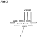
Abb. 2 :1 : Glas- oder Silicapartikel. Die plättchenförmigen Partikel sind parallel ausgerichtet und überlappen sich in vertikaler Richtung, so dass effektiv die Wasserdiffusion verhindert wird. -
Abb.3 :1 : Mittelwert der Messungen des Lichtstromes von 50 LEDs, welche eine separate Wasserdiffusions-Barriere-Schicht aufweisen.- 2: Mittelwert der Messungen des Lichtstromes von 50 LEDs, die eine Wasserdiffusions-Barriere aufweisen. Dabei wurde der grüne Orthosilikatleuchtstoff mit plättchenförmigen Partikeln gemischt.
- 3: Mittelwert der Messungen des Lichtstromes von 50 LEDs, die keine Wasserdiffusions-Barriere aufweisen.
Claims (9)
- Ein elektrolumineszierendes Bauelement mit einer Vergussmasse auf der Basis mindestens eines transparenten Silicon- oder Epoxyharzes enthaltend anorganische Leuchtstoffpartikel sowie Glas- und/oder Silicapartikel auf einer UV- oder blauen Leuchtdiode, dadurch gekennzeichnet, dass die Glas- und/oder Silicapartikel plättchenförmig sind und einen Durchmesser von 5 bis 20 µm und eine Dicke von 0,1 bis 5 µm besitzen.
- Ein elektrolumineszierendes Bauelement nach Anspruch 1, dadurch gekennzeichnet, dass die Glas- und/oder Silicapartikel und die Leuchtstoffpartikel in der Vergussmasse homogen verteilt sind.
- Ein elektrolumineszierendes Bauelement nach Anspruch 1, dadurch gekennzeichnet, dass die Glas- und/oder Silicapartikel in der Vergussmasse dispergiert und planparallel ausgerichtet sind und als separate Diffusionssperrschicht direkt auf einer zusätzlichen Vergussmasse, welche ausschließlich die Leuchtstoffpartikel enthält, angeordnet sind.
- Ein elektrolumineszierendes Bauelement nach einem oder mehreren der Ansprüche 1 bis 3, dadurch gekennzeichnet, dass der mittlere Korndurchmesser d50 der Leuchtstoffpartikel < 20 µm liegt.
- Ein elektrolumineszierendes Bauelement nach einem oder mehreren der Ansprüche 1 bis 4, dadurch gekennzeichnet, dass die anorganischen Leuchtstoffpartikel aus folgender Gruppe ausgewählt sind:
(Y, Gd, Lu, Sc, Sm, Tb)3 (AI, Ga)5O12:Ce (mit oder ohne Pr), (Ca, Sr, Ba)2SiO4:Eu, YSiO2N:Ce, Y2Si3O3N4:Ce, Gd2Si3O3N4:Ce, (Y,Gd,Tb,Lu)3Al5-xSixO12-xNx:Ce, BaMgAl10O17:Eu, SrAl2O4:Eu, Sr4Al14O25:Eu, (Ca,Sr,Ba)Si2N2O2:Eu, SrSiAl2O3N2:Eu, (Ca,Sr,Ba)2Si5N8:Eu, CaAlSiN3:Eu, Zink-Erdalkaliorthosilikate, Kupfer-Erdalkaliorthosilikate, Eisen-Erdalkaliorthosilikate, Molybdate, Wolframate, Vanadate, Gruppe-III Nitride, Oxide, jeweils einzeln oder Gemischen derselben mit einem oder mehreren Aktivatorionen wie Ce, Eu, Mn, Cr und/oder Bi - Ein elektrolumineszierendes Bauelement nach Anspruch 5, dadurch gekennzeichnet, dass die anorganischen Leuchtstoffpartikel ortho-Silikate sind.
- Verfahren zur Herstellung eines elektrolumineszierenden Bauelements nach einem oder mehreren der Ansprüche 1 bis 2 und 4 bis 6 mit einer Vergussmasse auf der Basis mindestens eines transparenten Silicon- oder Epoxyharzes enthaltend anorganische Leuchtstoffpartikel sowie Glas- und/oder Silicapartikel auf einer UV- oder blauen Leuchtdiode, gekennzeichnet durch die Verfahrensschritte:a) homogenes Mischen anorganischer Leuchtstoffpartikel mit pulverförmigen Glas- und/oder Silicapartikelnb) Dispergieren der Mischung aus Leuchtstoffen und Glas- und/oder Silicapartikeln mit dem transparenten Silicon- oder Epoxyharz.c) Beschichten der blauen Leuchtdiode mit Silicon- oder Epoxyharz, welches den Leuchtstoff und die Glas- und/oder Silicapartikel enthält.d) Aushärten der Beschichtung.
- Verfahren zur Herstellung eines elektrolumineszierenden Bauelements nach einem oder mehreren der Ansprüche 1 und 3 bis 6 mit einer Vergussmasse auf der Basis mindestens eines transparenten Silicon- oder Epoxyharzes enthaltend anorganische Leuchtstoffpartikel sowie Glas- und/oder Silicapartikel auf einer UV- oder blauen Leuchtdiode, gekennzeichnet durch die Verfahrensschritte:a) Dispergieren der anorganischen Leuchtstoffpartikel mit Silicon- oder Epoxyharz.b) Beschichten der Leuchtdiode mit der Mischung aus Leuchtstoffpartikel und Silicon- oder Epoxyharz.c) Aushärten der Beschichtungd) Dispergieren der Glas- oder Silicapartikel in Silicon- oder Epoxyharz.e) Herstellen einer Diffusionssperrschicht durch Beschichten der ausgehärteten Leuchtstoffbeschichtungf) Aushärten der Diffusionssperrschicht.
- Verfahren nach Anspruch 7 und/oder 8, dadurch gekennzeichnet, dass die Glas- und/oder Silicapartikel mit Silicium-organischen Verbindungen oberflächenbeschichtet werden.
Priority Applications (1)
| Application Number | Priority Date | Filing Date | Title |
|---|---|---|---|
| EP10784718.8A EP2519986B1 (de) | 2009-12-30 | 2010-12-01 | Vergussmasse als diffusionsbarriere für wassermoleküle |
Applications Claiming Priority (3)
| Application Number | Priority Date | Filing Date | Title |
|---|---|---|---|
| EP09016115 | 2009-12-30 | ||
| PCT/EP2010/007271 WO2011079900A1 (de) | 2009-12-30 | 2010-12-01 | Vergussmasse als diffusionsbarriere für wassermoleküle |
| EP10784718.8A EP2519986B1 (de) | 2009-12-30 | 2010-12-01 | Vergussmasse als diffusionsbarriere für wassermoleküle |
Publications (2)
| Publication Number | Publication Date |
|---|---|
| EP2519986A1 EP2519986A1 (de) | 2012-11-07 |
| EP2519986B1 true EP2519986B1 (de) | 2018-09-12 |
Family
ID=43467010
Family Applications (1)
| Application Number | Title | Priority Date | Filing Date |
|---|---|---|---|
| EP10784718.8A Not-in-force EP2519986B1 (de) | 2009-12-30 | 2010-12-01 | Vergussmasse als diffusionsbarriere für wassermoleküle |
Country Status (8)
| Country | Link |
|---|---|
| US (1) | US9093623B2 (de) |
| EP (1) | EP2519986B1 (de) |
| JP (1) | JP5767245B2 (de) |
| KR (1) | KR101795091B1 (de) |
| CN (1) | CN102714265A (de) |
| SG (1) | SG181935A1 (de) |
| TW (1) | TWI527847B (de) |
| WO (1) | WO2011079900A1 (de) |
Families Citing this family (16)
| Publication number | Priority date | Publication date | Assignee | Title |
|---|---|---|---|---|
| DE102011116229A1 (de) * | 2011-10-17 | 2013-04-18 | Osram Opto Semiconductors Gmbh | Keramisches Konversionselement, optoelektronisches Bauelement mit einem keramischen Konversionselement und Verfahren zur Herstellung eines keramischen Konversionselements |
| DE102011116230B4 (de) | 2011-10-17 | 2018-10-25 | Osram Opto Semiconductors Gmbh | Keramisches Konversionselement, optoelektronisches Halbleiterbauelement mit einem keramischen Konversionselement und Verfahren zur Herstellung eines keramischen Konversionselements |
| JP2015516691A (ja) | 2012-05-14 | 2015-06-11 | コーニンクレッカ フィリップス エヌ ヴェ | ナノ構造蛍光体を有する発光装置 |
| JP2014022508A (ja) * | 2012-07-17 | 2014-02-03 | Konica Minolta Inc | Led装置及びその製造方法 |
| DE102012108939A1 (de) * | 2012-09-21 | 2014-03-27 | Osram Opto Semiconductors Gmbh | Optoelektronisches Bauelement umfassend ein transparentes Auskoppelelement |
| DE102013210103A1 (de) * | 2013-05-29 | 2014-12-18 | Osram Opto Semiconductors Gmbh | Optoelektronisches Bauelement |
| CN103811634A (zh) * | 2014-01-26 | 2014-05-21 | 佛山市国星光电股份有限公司 | 封装胶体表面哑光的led器件及其封装方法及led显示屏 |
| KR102369932B1 (ko) | 2014-11-10 | 2022-03-04 | 삼성전자주식회사 | 불화물계 형광체, 발광장치, 불화물계 형광체 제조방법 및 발광장치 제조방법 |
| US9871176B2 (en) * | 2015-02-02 | 2018-01-16 | Ferro Corporation | Glass compositions and glass frit composites for use in optical applications |
| KR102432725B1 (ko) * | 2015-02-23 | 2022-08-17 | 코닌클리케 필립스 엔.브이. | 안정적인 유속 출력 대 온도를 갖는 백색 인광체 변환 led |
| JP6470157B2 (ja) * | 2015-09-30 | 2019-02-13 | 関西ペイント株式会社 | 発光素子封止用樹脂組成物 |
| JP6615557B2 (ja) * | 2015-09-30 | 2019-12-04 | 日亜化学工業株式会社 | 発光装置及びその製造方法 |
| JP6387954B2 (ja) * | 2015-12-24 | 2018-09-12 | 日亜化学工業株式会社 | 波長変換部材を用いた発光装置の製造方法 |
| JP2018056512A (ja) * | 2016-09-30 | 2018-04-05 | デクセリアルズ株式会社 | 発光装置、及び発光装置の製造方法 |
| JP7580206B2 (ja) * | 2020-05-25 | 2024-11-11 | スタンレー電気株式会社 | 半導体発光装置 |
| CN114695629A (zh) * | 2020-12-25 | 2022-07-01 | 惠州视维新技术有限公司 | 一种led封装用的封装材料及led |
Family Cites Families (28)
| Publication number | Priority date | Publication date | Assignee | Title |
|---|---|---|---|---|
| US5300558A (en) * | 1991-04-05 | 1994-04-05 | Mitsui Petrochemical Industries, Ltd. | Curable resin coating composition |
| US6630018B2 (en) | 1991-10-18 | 2003-10-07 | MERCK Patent Gesellschaft mit beschränkter Haftung | Colored and coated plateletlike pigments |
| JP3242561B2 (ja) | 1995-09-14 | 2001-12-25 | メルク・ジヤパン株式会社 | 薄片状酸化アルミニウム、真珠光沢顔料及びその製造方法 |
| DE19618564A1 (de) | 1996-05-09 | 1997-11-13 | Merck Patent Gmbh | Plättchenförmiges Titandioxidpigment |
| DE19638667C2 (de) | 1996-09-20 | 2001-05-17 | Osram Opto Semiconductors Gmbh | Mischfarbiges Licht abstrahlendes Halbleiterbauelement mit Lumineszenzkonversionselement |
| JP3417415B1 (ja) | 2001-01-24 | 2003-06-16 | 日亜化学工業株式会社 | エポキシ樹脂組成物、その製造方法、それを用いた光半導体素子 |
| US6833191B2 (en) * | 2001-11-20 | 2004-12-21 | Encap Technologies, Llc | Microencapsulated particles and process for manufacturing same |
| CN100556687C (zh) * | 2002-09-12 | 2009-11-04 | 日本板硝子株式会社 | 覆发光膜产品 |
| JP2004149782A (ja) * | 2002-10-09 | 2004-05-27 | Mitsubishi Chemicals Corp | 熱可塑性樹脂組成物及びそれを用いてなる成形体 |
| JP4288940B2 (ja) * | 2002-12-06 | 2009-07-01 | 日亜化学工業株式会社 | エポキシ樹脂組成物 |
| JP2004273798A (ja) * | 2003-03-10 | 2004-09-30 | Toyoda Gosei Co Ltd | 発光デバイス |
| US20070013057A1 (en) * | 2003-05-05 | 2007-01-18 | Joseph Mazzochette | Multicolor LED assembly with improved color mixing |
| US6841888B2 (en) * | 2003-06-04 | 2005-01-11 | Yazaki Corporation | Encapsulant for opto-electronic devices and method for making it |
| DE102004034166B4 (de) * | 2003-07-17 | 2015-08-20 | Toyoda Gosei Co., Ltd. | Lichtemittierende Vorrichtung |
| EP1770126B1 (de) * | 2004-07-20 | 2018-01-10 | Teijin Chemicals, Ltd. | Aromatisches polycarbonat enthaltende harzzusammensetzung und herstellungsverfahren dafür |
| US8324641B2 (en) * | 2007-06-29 | 2012-12-04 | Ledengin, Inc. | Matrix material including an embedded dispersion of beads for a light-emitting device |
| DE102006004397A1 (de) * | 2005-09-30 | 2007-04-05 | Osram Opto Semiconductors Gmbh | Elektromagnetische Strahlung emittierendes optoelektronisches Bauelement und Verfahren zur Herstellung eines optoelektronischen Bauelements |
| US20070125984A1 (en) * | 2005-12-01 | 2007-06-07 | Sarnoff Corporation | Phosphors protected against moisture and LED lighting devices |
| US20070241661A1 (en) * | 2006-04-12 | 2007-10-18 | Yin Chua B | High light output lamps having a phosphor embedded glass/ceramic layer |
| JP5090802B2 (ja) * | 2006-06-28 | 2012-12-05 | ソウル セミコンダクター カンパニー リミテッド | 蛍光体及びその製造方法並びに発光ダイオード |
| GB2442535B (en) * | 2006-10-05 | 2011-07-13 | Ngf Europ Ltd | Method and articles |
| TWI326923B (en) * | 2007-03-07 | 2010-07-01 | Lite On Technology Corp | White light emitting diode |
| US7999283B2 (en) * | 2007-06-14 | 2011-08-16 | Cree, Inc. | Encapsulant with scatterer to tailor spatial emission pattern and color uniformity in light emitting diodes |
| TW200921929A (en) * | 2007-11-02 | 2009-05-16 | Innolux Display Corp | Light emitting diode |
| JP2009120437A (ja) * | 2007-11-14 | 2009-06-04 | Niigata Univ | シロキサンをグラフト化したシリカ及び高透明シリコーン組成物並びに該組成物で封止した発光半導体装置 |
| US20090130471A1 (en) * | 2007-11-16 | 2009-05-21 | E.I. Du Pont De Nemours And Company | Thermally conductive plastic resin composition |
| US20090261708A1 (en) * | 2008-04-21 | 2009-10-22 | Motorola, Inc. | Glass-phosphor capping structure for leds |
| CN102376860A (zh) * | 2010-08-05 | 2012-03-14 | 夏普株式会社 | 发光装置及其制造方法 |
-
2010
- 2010-12-01 SG SG2012047171A patent/SG181935A1/en unknown
- 2010-12-01 WO PCT/EP2010/007271 patent/WO2011079900A1/de not_active Ceased
- 2010-12-01 JP JP2012546375A patent/JP5767245B2/ja not_active Expired - Fee Related
- 2010-12-01 CN CN2010800595375A patent/CN102714265A/zh active Pending
- 2010-12-01 KR KR1020127020097A patent/KR101795091B1/ko not_active Expired - Fee Related
- 2010-12-01 US US13/519,945 patent/US9093623B2/en not_active Expired - Fee Related
- 2010-12-01 EP EP10784718.8A patent/EP2519986B1/de not_active Not-in-force
- 2010-12-29 TW TW099146698A patent/TWI527847B/zh not_active IP Right Cessation
Non-Patent Citations (1)
| Title |
|---|
| None * |
Also Published As
| Publication number | Publication date |
|---|---|
| US9093623B2 (en) | 2015-07-28 |
| US20120329184A1 (en) | 2012-12-27 |
| JP2013516747A (ja) | 2013-05-13 |
| TW201136998A (en) | 2011-11-01 |
| CN102714265A (zh) | 2012-10-03 |
| JP5767245B2 (ja) | 2015-08-19 |
| EP2519986A1 (de) | 2012-11-07 |
| WO2011079900A1 (de) | 2011-07-07 |
| TWI527847B (zh) | 2016-04-01 |
| SG181935A1 (en) | 2012-08-30 |
| KR101795091B1 (ko) | 2017-11-07 |
| KR20120107127A (ko) | 2012-09-28 |
Similar Documents
| Publication | Publication Date | Title |
|---|---|---|
| EP2519986B1 (de) | Vergussmasse als diffusionsbarriere für wassermoleküle | |
| EP2209869B1 (de) | Oberflächenmodifizierte leuchstoffe | |
| EP2229424B1 (de) | Oberflächenmodifizierte konversionsleuchtstoffe | |
| EP2576725B1 (de) | Leuchtstoffe | |
| EP2207866B1 (de) | Beschichtete leuchtstoffpartikel mit brechungsindex-anpassung | |
| EP2212401B1 (de) | Verfahren zur herstellung von beschichteten leuchtstoffen | |
| EP2356195A1 (de) | Oberflächenmodifizierte silikat-leuchtstoffe | |
| DE102010045368A1 (de) | Silicophosphat-Leuchtstoffe | |
| DE102010031755A1 (de) | Aluminat-Leuchtstoffe | |
| EP2488602A1 (de) | Verfahren zur beschichtung eines silikat-leuchtstoffs | |
| JP5443662B2 (ja) | 耐湿性蛍光体粒子粉末の製造方法及び該製造方法により得られた耐湿性蛍光体粒子粉末を用いたled素子または分散型el素子 | |
| WO2012045393A1 (de) | Mn-aktivierte leuchtstoffe | |
| EP2596681B1 (de) | Carbodiimid-leuchtstoffe | |
| EP2683790A1 (de) | Carbodiimid-leuchtstoffe | |
| DE112017004937T5 (de) | Lichtemittierendes Gerät und Verfahren zum Herstellen desselben | |
| EP2619283B1 (de) | Silicat-leuchtstoffe | |
| DE112022002894T5 (de) | Fluoridleuchtstoff, verfahren zu seiner herstellung und lichtemissionsvorrichtung |
Legal Events
| Date | Code | Title | Description |
|---|---|---|---|
| PUAI | Public reference made under article 153(3) epc to a published international application that has entered the european phase |
Free format text: ORIGINAL CODE: 0009012 |
|
| 17P | Request for examination filed |
Effective date: 20120507 |
|
| AK | Designated contracting states |
Kind code of ref document: A1 Designated state(s): AL AT BE BG CH CY CZ DE DK EE ES FI FR GB GR HR HU IE IS IT LI LT LU LV MC MK MT NL NO PL PT RO RS SE SI SK SM TR |
|
| DAX | Request for extension of the european patent (deleted) | ||
| GRAP | Despatch of communication of intention to grant a patent |
Free format text: ORIGINAL CODE: EPIDOSNIGR1 |
|
| INTG | Intention to grant announced |
Effective date: 20180523 |
|
| GRAS | Grant fee paid |
Free format text: ORIGINAL CODE: EPIDOSNIGR3 |
|
| GRAA | (expected) grant |
Free format text: ORIGINAL CODE: 0009210 |
|
| AK | Designated contracting states |
Kind code of ref document: B1 Designated state(s): AL AT BE BG CH CY CZ DE DK EE ES FI FR GB GR HR HU IE IS IT LI LT LU LV MC MK MT NL NO PL PT RO RS SE SI SK SM TR |
|
| REG | Reference to a national code |
Ref country code: GB Ref legal event code: FG4D Free format text: NOT ENGLISH |
|
| REG | Reference to a national code |
Ref country code: CH Ref legal event code: EP |
|
| REG | Reference to a national code |
Ref country code: IE Ref legal event code: FG4D Free format text: LANGUAGE OF EP DOCUMENT: GERMAN |
|
| REG | Reference to a national code |
Ref country code: DE Ref legal event code: R096 Ref document number: 502010015368 Country of ref document: DE |
|
| REG | Reference to a national code |
Ref country code: AT Ref legal event code: REF Ref document number: 1041608 Country of ref document: AT Kind code of ref document: T Effective date: 20181015 |
|
| REG | Reference to a national code |
Ref country code: NL Ref legal event code: FP |
|
| PGFP | Annual fee paid to national office [announced via postgrant information from national office to epo] |
Ref country code: NL Payment date: 20181017 Year of fee payment: 9 |
|
| REG | Reference to a national code |
Ref country code: LT Ref legal event code: MG4D |
|
| PG25 | Lapsed in a contracting state [announced via postgrant information from national office to epo] |
Ref country code: SE Free format text: LAPSE BECAUSE OF FAILURE TO SUBMIT A TRANSLATION OF THE DESCRIPTION OR TO PAY THE FEE WITHIN THE PRESCRIBED TIME-LIMIT Effective date: 20180912 Ref country code: NO Free format text: LAPSE BECAUSE OF FAILURE TO SUBMIT A TRANSLATION OF THE DESCRIPTION OR TO PAY THE FEE WITHIN THE PRESCRIBED TIME-LIMIT Effective date: 20181212 Ref country code: GR Free format text: LAPSE BECAUSE OF FAILURE TO SUBMIT A TRANSLATION OF THE DESCRIPTION OR TO PAY THE FEE WITHIN THE PRESCRIBED TIME-LIMIT Effective date: 20181213 Ref country code: FI Free format text: LAPSE BECAUSE OF FAILURE TO SUBMIT A TRANSLATION OF THE DESCRIPTION OR TO PAY THE FEE WITHIN THE PRESCRIBED TIME-LIMIT Effective date: 20180912 Ref country code: RS Free format text: LAPSE BECAUSE OF FAILURE TO SUBMIT A TRANSLATION OF THE DESCRIPTION OR TO PAY THE FEE WITHIN THE PRESCRIBED TIME-LIMIT Effective date: 20180912 Ref country code: BG Free format text: LAPSE BECAUSE OF FAILURE TO SUBMIT A TRANSLATION OF THE DESCRIPTION OR TO PAY THE FEE WITHIN THE PRESCRIBED TIME-LIMIT Effective date: 20181212 Ref country code: LT Free format text: LAPSE BECAUSE OF FAILURE TO SUBMIT A TRANSLATION OF THE DESCRIPTION OR TO PAY THE FEE WITHIN THE PRESCRIBED TIME-LIMIT Effective date: 20180912 |
|
| PGFP | Annual fee paid to national office [announced via postgrant information from national office to epo] |
Ref country code: DE Payment date: 20181120 Year of fee payment: 9 |
|
| PG25 | Lapsed in a contracting state [announced via postgrant information from national office to epo] |
Ref country code: AL Free format text: LAPSE BECAUSE OF FAILURE TO SUBMIT A TRANSLATION OF THE DESCRIPTION OR TO PAY THE FEE WITHIN THE PRESCRIBED TIME-LIMIT Effective date: 20180912 Ref country code: LV Free format text: LAPSE BECAUSE OF FAILURE TO SUBMIT A TRANSLATION OF THE DESCRIPTION OR TO PAY THE FEE WITHIN THE PRESCRIBED TIME-LIMIT Effective date: 20180912 Ref country code: HR Free format text: LAPSE BECAUSE OF FAILURE TO SUBMIT A TRANSLATION OF THE DESCRIPTION OR TO PAY THE FEE WITHIN THE PRESCRIBED TIME-LIMIT Effective date: 20180912 |
|
| PGFP | Annual fee paid to national office [announced via postgrant information from national office to epo] |
Ref country code: GB Payment date: 20181128 Year of fee payment: 9 |
|
| PG25 | Lapsed in a contracting state [announced via postgrant information from national office to epo] |
Ref country code: EE Free format text: LAPSE BECAUSE OF FAILURE TO SUBMIT A TRANSLATION OF THE DESCRIPTION OR TO PAY THE FEE WITHIN THE PRESCRIBED TIME-LIMIT Effective date: 20180912 Ref country code: PL Free format text: LAPSE BECAUSE OF FAILURE TO SUBMIT A TRANSLATION OF THE DESCRIPTION OR TO PAY THE FEE WITHIN THE PRESCRIBED TIME-LIMIT Effective date: 20180912 Ref country code: ES Free format text: LAPSE BECAUSE OF FAILURE TO SUBMIT A TRANSLATION OF THE DESCRIPTION OR TO PAY THE FEE WITHIN THE PRESCRIBED TIME-LIMIT Effective date: 20180912 Ref country code: IS Free format text: LAPSE BECAUSE OF FAILURE TO SUBMIT A TRANSLATION OF THE DESCRIPTION OR TO PAY THE FEE WITHIN THE PRESCRIBED TIME-LIMIT Effective date: 20190112 Ref country code: CZ Free format text: LAPSE BECAUSE OF FAILURE TO SUBMIT A TRANSLATION OF THE DESCRIPTION OR TO PAY THE FEE WITHIN THE PRESCRIBED TIME-LIMIT Effective date: 20180912 Ref country code: RO Free format text: LAPSE BECAUSE OF FAILURE TO SUBMIT A TRANSLATION OF THE DESCRIPTION OR TO PAY THE FEE WITHIN THE PRESCRIBED TIME-LIMIT Effective date: 20180912 Ref country code: IT Free format text: LAPSE BECAUSE OF FAILURE TO SUBMIT A TRANSLATION OF THE DESCRIPTION OR TO PAY THE FEE WITHIN THE PRESCRIBED TIME-LIMIT Effective date: 20180912 |
|
| PG25 | Lapsed in a contracting state [announced via postgrant information from national office to epo] |
Ref country code: SK Free format text: LAPSE BECAUSE OF FAILURE TO SUBMIT A TRANSLATION OF THE DESCRIPTION OR TO PAY THE FEE WITHIN THE PRESCRIBED TIME-LIMIT Effective date: 20180912 Ref country code: SM Free format text: LAPSE BECAUSE OF FAILURE TO SUBMIT A TRANSLATION OF THE DESCRIPTION OR TO PAY THE FEE WITHIN THE PRESCRIBED TIME-LIMIT Effective date: 20180912 Ref country code: PT Free format text: LAPSE BECAUSE OF FAILURE TO SUBMIT A TRANSLATION OF THE DESCRIPTION OR TO PAY THE FEE WITHIN THE PRESCRIBED TIME-LIMIT Effective date: 20190112 |
|
| REG | Reference to a national code |
Ref country code: DE Ref legal event code: R097 Ref document number: 502010015368 Country of ref document: DE |
|
| PLBE | No opposition filed within time limit |
Free format text: ORIGINAL CODE: 0009261 |
|
| STAA | Information on the status of an ep patent application or granted ep patent |
Free format text: STATUS: NO OPPOSITION FILED WITHIN TIME LIMIT |
|
| PG25 | Lapsed in a contracting state [announced via postgrant information from national office to epo] |
Ref country code: DK Free format text: LAPSE BECAUSE OF FAILURE TO SUBMIT A TRANSLATION OF THE DESCRIPTION OR TO PAY THE FEE WITHIN THE PRESCRIBED TIME-LIMIT Effective date: 20180912 |
|
| REG | Reference to a national code |
Ref country code: CH Ref legal event code: PL |
|
| 26N | No opposition filed |
Effective date: 20190613 |
|
| PG25 | Lapsed in a contracting state [announced via postgrant information from national office to epo] |
Ref country code: MC Free format text: LAPSE BECAUSE OF FAILURE TO SUBMIT A TRANSLATION OF THE DESCRIPTION OR TO PAY THE FEE WITHIN THE PRESCRIBED TIME-LIMIT Effective date: 20180912 Ref country code: LU Free format text: LAPSE BECAUSE OF NON-PAYMENT OF DUE FEES Effective date: 20181201 Ref country code: SI Free format text: LAPSE BECAUSE OF FAILURE TO SUBMIT A TRANSLATION OF THE DESCRIPTION OR TO PAY THE FEE WITHIN THE PRESCRIBED TIME-LIMIT Effective date: 20180912 |
|
| REG | Reference to a national code |
Ref country code: IE Ref legal event code: MM4A |
|
| REG | Reference to a national code |
Ref country code: BE Ref legal event code: MM Effective date: 20181231 |
|
| PG25 | Lapsed in a contracting state [announced via postgrant information from national office to epo] |
Ref country code: IE Free format text: LAPSE BECAUSE OF NON-PAYMENT OF DUE FEES Effective date: 20181201 Ref country code: FR Free format text: LAPSE BECAUSE OF NON-PAYMENT OF DUE FEES Effective date: 20181231 |
|
| PG25 | Lapsed in a contracting state [announced via postgrant information from national office to epo] |
Ref country code: BE Free format text: LAPSE BECAUSE OF NON-PAYMENT OF DUE FEES Effective date: 20181231 |
|
| PG25 | Lapsed in a contracting state [announced via postgrant information from national office to epo] |
Ref country code: CH Free format text: LAPSE BECAUSE OF NON-PAYMENT OF DUE FEES Effective date: 20181231 Ref country code: LI Free format text: LAPSE BECAUSE OF NON-PAYMENT OF DUE FEES Effective date: 20181231 |
|
| PG25 | Lapsed in a contracting state [announced via postgrant information from national office to epo] |
Ref country code: MT Free format text: LAPSE BECAUSE OF FAILURE TO SUBMIT A TRANSLATION OF THE DESCRIPTION OR TO PAY THE FEE WITHIN THE PRESCRIBED TIME-LIMIT Effective date: 20180912 |
|
| REG | Reference to a national code |
Ref country code: AT Ref legal event code: MM01 Ref document number: 1041608 Country of ref document: AT Kind code of ref document: T Effective date: 20181201 |
|
| PG25 | Lapsed in a contracting state [announced via postgrant information from national office to epo] |
Ref country code: TR Free format text: LAPSE BECAUSE OF FAILURE TO SUBMIT A TRANSLATION OF THE DESCRIPTION OR TO PAY THE FEE WITHIN THE PRESCRIBED TIME-LIMIT Effective date: 20180912 |
|
| PG25 | Lapsed in a contracting state [announced via postgrant information from national office to epo] |
Ref country code: AT Free format text: LAPSE BECAUSE OF NON-PAYMENT OF DUE FEES Effective date: 20181201 |
|
| PG25 | Lapsed in a contracting state [announced via postgrant information from national office to epo] |
Ref country code: CY Free format text: LAPSE BECAUSE OF FAILURE TO SUBMIT A TRANSLATION OF THE DESCRIPTION OR TO PAY THE FEE WITHIN THE PRESCRIBED TIME-LIMIT Effective date: 20180912 Ref country code: HU Free format text: LAPSE BECAUSE OF FAILURE TO SUBMIT A TRANSLATION OF THE DESCRIPTION OR TO PAY THE FEE WITHIN THE PRESCRIBED TIME-LIMIT; INVALID AB INITIO Effective date: 20101201 Ref country code: MK Free format text: LAPSE BECAUSE OF NON-PAYMENT OF DUE FEES Effective date: 20180912 |
|
| REG | Reference to a national code |
Ref country code: DE Ref legal event code: R119 Ref document number: 502010015368 Country of ref document: DE |
|
| REG | Reference to a national code |
Ref country code: NL Ref legal event code: MM Effective date: 20200101 |
|
| GBPC | Gb: european patent ceased through non-payment of renewal fee |
Effective date: 20191201 |
|
| PG25 | Lapsed in a contracting state [announced via postgrant information from national office to epo] |
Ref country code: NL Free format text: LAPSE BECAUSE OF NON-PAYMENT OF DUE FEES Effective date: 20200101 |
|
| PG25 | Lapsed in a contracting state [announced via postgrant information from national office to epo] |
Ref country code: DE Free format text: LAPSE BECAUSE OF NON-PAYMENT OF DUE FEES Effective date: 20200701 Ref country code: GB Free format text: LAPSE BECAUSE OF NON-PAYMENT OF DUE FEES Effective date: 20191201 |