EP2519986B1 - Matériau d'enrobage en tant que barrière de diffusion envers des molécules d'eau - Google Patents
Matériau d'enrobage en tant que barrière de diffusion envers des molécules d'eau Download PDFInfo
- Publication number
- EP2519986B1 EP2519986B1 EP10784718.8A EP10784718A EP2519986B1 EP 2519986 B1 EP2519986 B1 EP 2519986B1 EP 10784718 A EP10784718 A EP 10784718A EP 2519986 B1 EP2519986 B1 EP 2519986B1
- Authority
- EP
- European Patent Office
- Prior art keywords
- glass
- particles
- silica particles
- epoxy resin
- silicone
- Prior art date
- Legal status (The legal status is an assumption and is not a legal conclusion. Google has not performed a legal analysis and makes no representation as to the accuracy of the status listed.)
- Not-in-force
Links
Images


Classifications
-
- H—ELECTRICITY
- H01—ELECTRIC ELEMENTS
- H01L—SEMICONDUCTOR DEVICES NOT COVERED BY CLASS H10
- H01L33/00—Semiconductor devices with at least one potential-jump barrier or surface barrier specially adapted for light emission; Processes or apparatus specially adapted for the manufacture or treatment thereof or of parts thereof; Details thereof
- H01L33/48—Semiconductor devices with at least one potential-jump barrier or surface barrier specially adapted for light emission; Processes or apparatus specially adapted for the manufacture or treatment thereof or of parts thereof; Details thereof characterised by the semiconductor body packages
- H01L33/52—Encapsulations
- H01L33/56—Materials, e.g. epoxy or silicone resin
-
- H—ELECTRICITY
- H01—ELECTRIC ELEMENTS
- H01L—SEMICONDUCTOR DEVICES NOT COVERED BY CLASS H10
- H01L33/00—Semiconductor devices with at least one potential-jump barrier or surface barrier specially adapted for light emission; Processes or apparatus specially adapted for the manufacture or treatment thereof or of parts thereof; Details thereof
- H01L33/48—Semiconductor devices with at least one potential-jump barrier or surface barrier specially adapted for light emission; Processes or apparatus specially adapted for the manufacture or treatment thereof or of parts thereof; Details thereof characterised by the semiconductor body packages
- H01L33/50—Wavelength conversion elements
- H01L33/501—Wavelength conversion elements characterised by the materials, e.g. binder
-
- H—ELECTRICITY
- H01—ELECTRIC ELEMENTS
- H01L—SEMICONDUCTOR DEVICES NOT COVERED BY CLASS H10
- H01L2933/00—Details relating to devices covered by the group H01L33/00 but not provided for in its subgroups
- H01L2933/0008—Processes
- H01L2933/0033—Processes relating to semiconductor body packages
- H01L2933/0041—Processes relating to semiconductor body packages relating to wavelength conversion elements
-
- H—ELECTRICITY
- H01—ELECTRIC ELEMENTS
- H01L—SEMICONDUCTOR DEVICES NOT COVERED BY CLASS H10
- H01L2933/00—Details relating to devices covered by the group H01L33/00 but not provided for in its subgroups
- H01L2933/0091—Scattering means in or on the semiconductor body or semiconductor body package
-
- H—ELECTRICITY
- H01—ELECTRIC ELEMENTS
- H01L—SEMICONDUCTOR DEVICES NOT COVERED BY CLASS H10
- H01L33/00—Semiconductor devices with at least one potential-jump barrier or surface barrier specially adapted for light emission; Processes or apparatus specially adapted for the manufacture or treatment thereof or of parts thereof; Details thereof
- H01L33/48—Semiconductor devices with at least one potential-jump barrier or surface barrier specially adapted for light emission; Processes or apparatus specially adapted for the manufacture or treatment thereof or of parts thereof; Details thereof characterised by the semiconductor body packages
- H01L33/50—Wavelength conversion elements
- H01L33/501—Wavelength conversion elements characterised by the materials, e.g. binder
- H01L33/502—Wavelength conversion materials
Definitions
- the invention relates to a potting compound based on a transparent epoxy or silicone resin for uses in an electroluminescent device, which preferably emits white light and a method for producing such potting compounds.
- the potting compound serves as a diffusion barrier for water molecules through the use of glass or silica platelets.
- Commercial white pc LEDs consist of a chip emitting in the blue spectral region and a coating of silicone or epoxy resin containing one or more phosphors.
- the phosphors are often based on silicate, sulfidic, nitridic or oxynitride materials. These materials have the property of decomposing in the presence of the slightest traces of moisture.
- a wavelength-converting potting compound which consists of epoxy resin and contains inorganic phosphor pigments.
- the phosphor pigments can be provided with a silicone coating.
- the object of the present invention is therefore to provide casting compounds which do not have one or more of the abovementioned disadvantages.
- the present invention thus relates to an electroluminescent component with a potting compound based on at least one transparent silicone or epoxy resin containing inorganic phosphor particles and platelet-shaped glass and / or silica particles, on a UV or blue light-emitting diode.
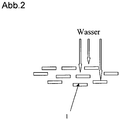
- the glass or silica particles and the phosphor particles are homogeneously distributed in the potting compound (see Fig. 1 A)
- the platelet-shaped glass or silica particles are dispersed in the potting compound and aligned plane-parallel and as a separate diffusion barrier layer directly on a additional potting compound, which contains only the phosphor particles, arranged (see Fig. 1B
- the glass and silica particles have a diameter of 5 to 20 ⁇ m and a thickness of 0.1 to 5 ⁇ m.
- the average particle diameter d 50 of the phosphor particles is preferably ⁇ 20 ⁇ m.
- the particles can be surface-coated.
- the platelet-shaped particles are then wet-chemically coated with silicones / silanes or by vapor deposition. These organosilicon compounds react with the surface OH groups of the platelet particles.
- the desired hydrophobicity of the particles, structure of the oligomer / polymer chains and the coupling (physical and / or chemical) to the resin are controlled.
- the phosphor particles consist of at least one of the following phosphor materials: (Y, Gd, Lu, Sc, Sm, Tb) 3 (Al, Ga) 5 O 12 : Ce (with or without Pr), (Ca, Sr, Ba) 2 SiO 4 : Eu, YSiO 2 N: Ce, Y 2 Si 3 O 3 N 4 : Ce, Gd 2 Si 3 O 3 N 4 : Ce, (Y, Gd, Tb, Lu) 3 Al 5-x Si x O 12-x N x : Ce, BaMgAl 10 O 17 : Eu, SrAl 2 O 4 : Eu, Sr 4 Al 14 O 25 : Eu, (Ca, Sr, Ba) Si 2 N 2 O 2 : Eu, SrSiAl 2 O 3 N 2 : Eu, (Ca, Sr, Ba) 2 Si 5 N 8 : Eu, CaAlSiN 3 : Eu, zinc-alkaline earth orthosilicates, copper-alkaline earth orthos
- Particularly preferred inorganic phosphor particles for producing white-luminescent optoelectronic components are ortho-silicates.
- the starting materials for the preparation of the phosphor particle consist of the base material (e.g., salt solutions of yttrium, aluminum, gadolinium, etc.) and at least one dopant (e.g., cerium).
- Suitable starting materials are inorganic and / or organic substances such as nitrates, halides, carbonates, bicarbonates, phosphates, carboxylates, alcoholates, acetates, oxalates, sulfates, organometallic compounds, hydroxides and / or oxides of metals, semimetals, transition metals and / or rare earths , which are dissolved and / or suspended in inorganic and / or organic liquids.
- Preferably mixed nitrate solutions, chloride or hydroxide solutions are used which contain the corresponding elements in the required stoichiometric ratio.
- the curing of the coating takes place at temperatures between 120 and 180 ° C, preferably at 150 ° C.
- the production of the glass and silica particles is carried out by conventional processes via a strip process from the corresponding alkali metal salts (eg for silica from a potassium or sodium water glass solution). The production process is described in detail in EP 763573 . EP 608388 and DE 19618564 described.
- the platelet-shaped glass or silica particles are surface-coated with organosilicon compounds (such as silicones or silanes) by wet-chemical means or by vapor deposition.
- organosilicon compounds such as silicones or silanes
- the potting compound may additionally be added light-scattering particles, so-called diffusers (such as CaF 2 ).
- diffusers such as CaF 2
- the potting compound may also contain adhesion promoters, water repellents, processing aids and / or thixotropic agents.
- a thixotropic agent for example, fumed silica can be used.
- the thixotropic agent serves to thicken the epoxy resin in order to reduce the sedimentation of the phosphor particles.
- processing aids are, for example, glycol ethers.
- bonding agent for example, functional alkoxysiloxane can be used, which improves the adhesion between phosphor particles and resin.
- liquid silicone wax which also serves to modify the phosphor particle surface, can be used as the hydrophobizing agent.
- silica or glass particles 100 g of the silica or glass particles are suspended in 1350 ml of deionized water while stirring vigorously.
- 4.0 g of a 1: 1 mixture of Silquest A-186 [beta- (3,4-epoxycyclohexyl) ethyltrimethoxysilane] and Silquest A-1310 [gamma-isocyanatopropyltriethoxysilane] added to the suspension within 60 minutes with moderate stirring. After the addition is then stirred for 15 min to complete the coupling of the silanes to the surface.
- the pH is corrected by means of 5 wt% H 2 SO 4 to 6.5.
- the suspension is then filtered off and washed free of salt with deionised water. Drying takes place at 130 ° C. for 20 hours.
- the powder thus obtained is then sieved by means of a sieve of 40 ⁇ m.
- silica or glass particles 100 g of the silica or glass particles are suspended in 1350 ml of deionized water while stirring vigorously.
- 6.0 g of a 1: 2 mixture of Silquest A-1110 [gamma-aminopropytrimethoxysilane] and Silquest A-1524 [gamma-ureapropyltrimethoxysilane] are metered into the suspension within 75 minutes with moderate stirring. After the addition is then stirred for 15 min to complete the coupling of the silanes to the surface.
- the pH is corrected by means of 5 wt% H 2 SO 4 to 6.5.
- the suspension is then filtered off and washed free of salt with deionised water.
- the drying takes place at 140 ° C. for 20 h.
- the powder thus obtained is then sieved by means of a sieve of 40 ⁇ m.
- the following mixtures are prepared in a Speedmixer® (speed 3000 rpm, duration: 5 min, room temperature): Each 50 ml of the two resin components JCR 6122 a and b 4% by weight of one of the green ortho-silicate phosphor and 2% of uncoated glass or silica particles or the compatibilized according to Example 1 A, B, or C platelet-shaped particles mixed.
- the platelet-shaped particles have an average diameter of 5 .mu.m to 20 .mu.m and a thickness distribution of 0.1 .mu.m to 5 .mu.m.
- the two resin mixtures are combined, stirred and degassed.
Landscapes
- Engineering & Computer Science (AREA)
- Microelectronics & Electronic Packaging (AREA)
- Manufacturing & Machinery (AREA)
- Computer Hardware Design (AREA)
- Power Engineering (AREA)
- Led Device Packages (AREA)
- Luminescent Compositions (AREA)
- Compositions Of Macromolecular Compounds (AREA)
- Electroluminescent Light Sources (AREA)
Claims (9)
- Composant électroluminescent avec une composition d'encapsulage qui est basée sur au moins une résine silicone ou époxy transparente qui comprend des particules de phosphore inorganiques et des particules de verre et/ou de silice sur une diode émettrice de lumière UV ou de lumière bleue, caractérisé en ce que les particules de verre et/ou de silice sont sous la forme de flocons et elles présentent un diamètre de 5 à 20 µm et une épaisseur de 0,1 à 5 µm.
- Composant électroluminescent selon la revendication 1, caractérisé en ce que les particules de verre et/ou de silice et les particules de phosphore sont distribuées de façon homogène dans la composition d'encapsulage.
- Composant électroluminescent selon la revendication 1, caractérisé en ce que les particules de verre et/ou de silice sont dispersées et alignées d'une manière à plans parallèles dans la composition d'encapsulage et sont agencées en tant que couche de barrière de diffusion séparée directement sur une composition d'encapsulage additionnelle qui comprend de façon exclusive les particules de phosphore.
- Composant électroluminescent selon une ou plusieurs des revendications 1 à 3, caractérisé en ce que le diamètre de particule moyen d50 des particules de phosphore est < 20 µm.
- Composant électroluminescent selon une ou plusieurs des revendications 1 à 4, caractérisé en ce que les particules de phosphore inorganiques sont sélectionnées parmi le groupe qui suit :
(Y, Gd, Lu, Sc, Sm, Tb)3 (Al, Ga)5O12:Ce (avec ou sans Pr), (Ca, Sr Ba)2SiO4:Eu, YSiO2N:Ce, Y2Si3O3N4:Ce, Gd2Si3O3N4:Ce, (Y,Gd,Tb,Lu)3Al5-xSixO12-xNx:Ce, BaMgAl10O17:Eu, SrAl2O4:Eu, Sr4Al14O25:Eu, (Ca,Sr,Ba)Si2N2O2:Eu, SrSiAl2O3N2:Eu, (Ca,Sr,Ba)2Si5N8:Eu, CaAlSiN3:Eu, les orthosilicates de zinc-alcalino-terreux, les orthosilicates de cuivre-alcalino-terreux, les orthosilicates de fer-alcalino-terreux, les molybdates, les tungstates, les vanadates, les nitrures du groupe III, les oxydes, dans chaque cas de façon individuelle ou selon des mélanges afférents avec un ou plusieurs ion(s) activateur(s), tels que Ce, Eu, Mn, Cr et/ou Bi. - Composant électroluminescent selon la revendication 5, caractérisé en ce que les particules de phosphore inorganiques sont des orthosilicates.
- Procédé pour la production d'un composant électroluminescent selon une ou plusieurs des revendications 1 et 2 et 4 à 6 avec une composition d'encapsulage qui est basée sur au moins une résine silicone ou époxy transparente qui comprend des particules de phosphore inorganiques et des particules de verre et/ou de silice sur une diode émettrice de lumière UV ou de lumière bleue, caractérisé par les étapes de procédé qui sont constituées par :a) le mélange homogène de particules de phosphore inorganiques avec des particules de verre et/ou de silice pulvérulentes ;b) la dispersion du mélange de particules de phosphore et de particules de verre et/ou de silice avec la résine silicone ou époxy transparente ;c) le revêtement de la diode émettrice de lumière bleue avec la résine silicone ou époxy qui comprend les particules de phosphore et les particules de verre et/ou de silice ; etd) le durcissement du revêtement.
- Procédé pour la production d'un composant électroluminescent selon une ou plusieurs des revendications 1 et 3 à 6 avec une composition d'encapsulage qui est basée sur au moins une résine silicone ou époxy transparente qui comprend des particules de phosphore inorganiques et des particules de verre et/ou de silice sur une diode émettrice de lumière UV ou de lumière bleue, caractérisé par les étapes de procédé qui sont constituées par :a) la dispersion des particules de phosphore inorganiques avec une résine silicone ou époxy ;b) le revêtement de la diode émettrice de lumière avec le mélange de particules de phosphore et de résine silicone ou époxy ;c) le durcissement du revêtement ;d) la dispersion des particules de verre ou de silice dans la résine silicone ou époxy ;e) la production d'une couche de barrière de diffusion par dépôt du revêtement de phosphore durci ; etf) le durcissement de la couche de barrière de diffusion.
- Procédé selon la revendication 7 et/ou 8, caractérisé en ce que les particules de verre et/ou de silice sont revêtues sur la surface avec des composés d'organosilicium.
Priority Applications (1)
| Application Number | Priority Date | Filing Date | Title |
|---|---|---|---|
| EP10784718.8A EP2519986B1 (fr) | 2009-12-30 | 2010-12-01 | Matériau d'enrobage en tant que barrière de diffusion envers des molécules d'eau |
Applications Claiming Priority (3)
| Application Number | Priority Date | Filing Date | Title |
|---|---|---|---|
| EP09016115 | 2009-12-30 | ||
| EP10784718.8A EP2519986B1 (fr) | 2009-12-30 | 2010-12-01 | Matériau d'enrobage en tant que barrière de diffusion envers des molécules d'eau |
| PCT/EP2010/007271 WO2011079900A1 (fr) | 2009-12-30 | 2010-12-01 | Matériau d'enrobage en tant que barrière de diffusion envers des molécules d'eau |
Publications (2)
| Publication Number | Publication Date |
|---|---|
| EP2519986A1 EP2519986A1 (fr) | 2012-11-07 |
| EP2519986B1 true EP2519986B1 (fr) | 2018-09-12 |
Family
ID=43467010
Family Applications (1)
| Application Number | Title | Priority Date | Filing Date |
|---|---|---|---|
| EP10784718.8A Not-in-force EP2519986B1 (fr) | 2009-12-30 | 2010-12-01 | Matériau d'enrobage en tant que barrière de diffusion envers des molécules d'eau |
Country Status (8)
| Country | Link |
|---|---|
| US (1) | US9093623B2 (fr) |
| EP (1) | EP2519986B1 (fr) |
| JP (1) | JP5767245B2 (fr) |
| KR (1) | KR101795091B1 (fr) |
| CN (1) | CN102714265A (fr) |
| SG (1) | SG181935A1 (fr) |
| TW (1) | TWI527847B (fr) |
| WO (1) | WO2011079900A1 (fr) |
Families Citing this family (14)
| Publication number | Priority date | Publication date | Assignee | Title |
|---|---|---|---|---|
| DE102011116229A1 (de) | 2011-10-17 | 2013-04-18 | Osram Opto Semiconductors Gmbh | Keramisches Konversionselement, optoelektronisches Bauelement mit einem keramischen Konversionselement und Verfahren zur Herstellung eines keramischen Konversionselements |
| DE102011116230B4 (de) | 2011-10-17 | 2018-10-25 | Osram Opto Semiconductors Gmbh | Keramisches Konversionselement, optoelektronisches Halbleiterbauelement mit einem keramischen Konversionselement und Verfahren zur Herstellung eines keramischen Konversionselements |
| JP2015516691A (ja) | 2012-05-14 | 2015-06-11 | コーニンクレッカ フィリップス エヌ ヴェ | ナノ構造蛍光体を有する発光装置 |
| JP2014022508A (ja) * | 2012-07-17 | 2014-02-03 | Konica Minolta Inc | Led装置及びその製造方法 |
| DE102012108939A1 (de) * | 2012-09-21 | 2014-03-27 | Osram Opto Semiconductors Gmbh | Optoelektronisches Bauelement umfassend ein transparentes Auskoppelelement |
| DE102013210103A1 (de) * | 2013-05-29 | 2014-12-18 | Osram Opto Semiconductors Gmbh | Optoelektronisches Bauelement |
| CN103811634A (zh) * | 2014-01-26 | 2014-05-21 | 佛山市国星光电股份有限公司 | 封装胶体表面哑光的led器件及其封装方法及led显示屏 |
| KR102369932B1 (ko) | 2014-11-10 | 2022-03-04 | 삼성전자주식회사 | 불화물계 형광체, 발광장치, 불화물계 형광체 제조방법 및 발광장치 제조방법 |
| US9871176B2 (en) * | 2015-02-02 | 2018-01-16 | Ferro Corporation | Glass compositions and glass frit composites for use in optical applications |
| CN107251244B (zh) * | 2015-02-23 | 2019-12-03 | 亮锐控股有限公司 | 具有相对于温度稳定的通量输出的白色磷光体转换led |
| JP6470157B2 (ja) * | 2015-09-30 | 2019-02-13 | 関西ペイント株式会社 | 発光素子封止用樹脂組成物 |
| JP6615557B2 (ja) * | 2015-09-30 | 2019-12-04 | 日亜化学工業株式会社 | 発光装置及びその製造方法 |
| JP6387954B2 (ja) * | 2015-12-24 | 2018-09-12 | 日亜化学工業株式会社 | 波長変換部材を用いた発光装置の製造方法 |
| JP2018056512A (ja) * | 2016-09-30 | 2018-04-05 | デクセリアルズ株式会社 | 発光装置、及び発光装置の製造方法 |
Family Cites Families (28)
| Publication number | Priority date | Publication date | Assignee | Title |
|---|---|---|---|---|
| CA2065092A1 (fr) * | 1991-04-05 | 1992-10-06 | Masayoshi Kurisu | Resine de revetement thermodurcissable et support d'enregistrement d'informations utilisant cette resine |
| KR100253774B1 (ko) | 1991-10-18 | 2000-05-01 | 플레믹 크리스티안 | 착색 및 피복된 판상 안료 |
| JP3242561B2 (ja) | 1995-09-14 | 2001-12-25 | メルク・ジヤパン株式会社 | 薄片状酸化アルミニウム、真珠光沢顔料及びその製造方法 |
| DE19618564A1 (de) | 1996-05-09 | 1997-11-13 | Merck Patent Gmbh | Plättchenförmiges Titandioxidpigment |
| DE19638667C2 (de) | 1996-09-20 | 2001-05-17 | Osram Opto Semiconductors Gmbh | Mischfarbiges Licht abstrahlendes Halbleiterbauelement mit Lumineszenzkonversionselement |
| JP3417415B1 (ja) * | 2001-01-24 | 2003-06-16 | 日亜化学工業株式会社 | エポキシ樹脂組成物、その製造方法、それを用いた光半導体素子 |
| US6833191B2 (en) * | 2001-11-20 | 2004-12-21 | Encap Technologies, Llc | Microencapsulated particles and process for manufacturing same |
| CN100556687C (zh) * | 2002-09-12 | 2009-11-04 | 日本板硝子株式会社 | 覆发光膜产品 |
| JP2004149782A (ja) * | 2002-10-09 | 2004-05-27 | Mitsubishi Chemicals Corp | 熱可塑性樹脂組成物及びそれを用いてなる成形体 |
| JP4288940B2 (ja) * | 2002-12-06 | 2009-07-01 | 日亜化学工業株式会社 | エポキシ樹脂組成物 |
| JP2004273798A (ja) * | 2003-03-10 | 2004-09-30 | Toyoda Gosei Co Ltd | 発光デバイス |
| US20070013057A1 (en) * | 2003-05-05 | 2007-01-18 | Joseph Mazzochette | Multicolor LED assembly with improved color mixing |
| US6841888B2 (en) * | 2003-06-04 | 2005-01-11 | Yazaki Corporation | Encapsulant for opto-electronic devices and method for making it |
| US7391153B2 (en) * | 2003-07-17 | 2008-06-24 | Toyoda Gosei Co., Ltd. | Light emitting device provided with a submount assembly for improved thermal dissipation |
| US8110622B2 (en) * | 2004-07-20 | 2012-02-07 | Teijin Chemicals Ltd. | Aromatic polycarbonate resin composition and manufacturing process thereof |
| US8324641B2 (en) * | 2007-06-29 | 2012-12-04 | Ledengin, Inc. | Matrix material including an embedded dispersion of beads for a light-emitting device |
| DE102006004397A1 (de) * | 2005-09-30 | 2007-04-05 | Osram Opto Semiconductors Gmbh | Elektromagnetische Strahlung emittierendes optoelektronisches Bauelement und Verfahren zur Herstellung eines optoelektronischen Bauelements |
| US20070125984A1 (en) * | 2005-12-01 | 2007-06-07 | Sarnoff Corporation | Phosphors protected against moisture and LED lighting devices |
| US20070241661A1 (en) * | 2006-04-12 | 2007-10-18 | Yin Chua B | High light output lamps having a phosphor embedded glass/ceramic layer |
| JP5090802B2 (ja) * | 2006-06-28 | 2012-12-05 | ソウル セミコンダクター カンパニー リミテッド | 蛍光体及びその製造方法並びに発光ダイオード |
| GB2442535B (en) * | 2006-10-05 | 2011-07-13 | Ngf Europ Ltd | Method and articles |
| TWI326923B (en) * | 2007-03-07 | 2010-07-01 | Lite On Technology Corp | White light emitting diode |
| US7999283B2 (en) * | 2007-06-14 | 2011-08-16 | Cree, Inc. | Encapsulant with scatterer to tailor spatial emission pattern and color uniformity in light emitting diodes |
| TW200921929A (en) * | 2007-11-02 | 2009-05-16 | Innolux Display Corp | Light emitting diode |
| JP2009120437A (ja) * | 2007-11-14 | 2009-06-04 | Niigata Univ | シロキサンをグラフト化したシリカ及び高透明シリコーン組成物並びに該組成物で封止した発光半導体装置 |
| US20090130471A1 (en) * | 2007-11-16 | 2009-05-21 | E.I. Du Pont De Nemours And Company | Thermally conductive plastic resin composition |
| US20090261708A1 (en) * | 2008-04-21 | 2009-10-22 | Motorola, Inc. | Glass-phosphor capping structure for leds |
| CN102376860A (zh) * | 2010-08-05 | 2012-03-14 | 夏普株式会社 | 发光装置及其制造方法 |
-
2010
- 2010-12-01 EP EP10784718.8A patent/EP2519986B1/fr not_active Not-in-force
- 2010-12-01 CN CN2010800595375A patent/CN102714265A/zh active Pending
- 2010-12-01 JP JP2012546375A patent/JP5767245B2/ja not_active Expired - Fee Related
- 2010-12-01 US US13/519,945 patent/US9093623B2/en not_active Expired - Fee Related
- 2010-12-01 KR KR1020127020097A patent/KR101795091B1/ko active IP Right Grant
- 2010-12-01 WO PCT/EP2010/007271 patent/WO2011079900A1/fr active Application Filing
- 2010-12-01 SG SG2012047171A patent/SG181935A1/en unknown
- 2010-12-29 TW TW099146698A patent/TWI527847B/zh not_active IP Right Cessation
Non-Patent Citations (1)
| Title |
|---|
| None * |
Also Published As
| Publication number | Publication date |
|---|---|
| WO2011079900A1 (fr) | 2011-07-07 |
| CN102714265A (zh) | 2012-10-03 |
| KR20120107127A (ko) | 2012-09-28 |
| JP5767245B2 (ja) | 2015-08-19 |
| TW201136998A (en) | 2011-11-01 |
| KR101795091B1 (ko) | 2017-11-07 |
| EP2519986A1 (fr) | 2012-11-07 |
| SG181935A1 (en) | 2012-08-30 |
| US9093623B2 (en) | 2015-07-28 |
| TWI527847B (zh) | 2016-04-01 |
| US20120329184A1 (en) | 2012-12-27 |
| JP2013516747A (ja) | 2013-05-13 |
Similar Documents
| Publication | Publication Date | Title |
|---|---|---|
| EP2519986B1 (fr) | Matériau d'enrobage en tant que barrière de diffusion envers des molécules d'eau | |
| EP2209869B1 (fr) | Substances luminescentes à surface modifiée | |
| EP2229424B1 (fr) | Substances luminescentes de conversion à surface modifiée | |
| EP2576725B1 (fr) | Substances luminescentes | |
| EP1897152B1 (fr) | Materiau convertisseur de longueur d'onde, composant optique electroluminescent et son procede de production | |
| EP2212401B1 (fr) | Procédé de fabrication de substances lumineuses revêtues | |
| JP5443662B2 (ja) | 耐湿性蛍光体粒子粉末の製造方法及び該製造方法により得られた耐湿性蛍光体粒子粉末を用いたled素子または分散型el素子 | |
| WO2010075908A1 (fr) | Substances luminescentes à surface modifiée à base de silicate | |
| EP2324096B1 (fr) | Nitrures 1-1-2 co-dopés | |
| EP2488602A1 (fr) | Procédé d'enrobage d'un luminophore de silicate | |
| EP2625247A1 (fr) | Luminophores activés par mn | |
| EP2596681B1 (fr) | Substances luminescentes de type carbodiimide | |
| WO2012119689A1 (fr) | Substances luminophores contenant des carbodiimides | |
| DE112017004937T5 (de) | Lichtemittierendes Gerät und Verfahren zum Herstellen desselben | |
| EP2619283B1 (fr) | Substances fluorescentes à base de silicate | |
| DE112022002894T5 (de) | Fluoridleuchtstoff, verfahren zu seiner herstellung und lichtemissionsvorrichtung |
Legal Events
| Date | Code | Title | Description |
|---|---|---|---|
| PUAI | Public reference made under article 153(3) epc to a published international application that has entered the european phase |
Free format text: ORIGINAL CODE: 0009012 |
|
| 17P | Request for examination filed |
Effective date: 20120507 |
|
| AK | Designated contracting states |
Kind code of ref document: A1 Designated state(s): AL AT BE BG CH CY CZ DE DK EE ES FI FR GB GR HR HU IE IS IT LI LT LU LV MC MK MT NL NO PL PT RO RS SE SI SK SM TR |
|
| DAX | Request for extension of the european patent (deleted) | ||
| GRAP | Despatch of communication of intention to grant a patent |
Free format text: ORIGINAL CODE: EPIDOSNIGR1 |
|
| INTG | Intention to grant announced |
Effective date: 20180523 |
|
| GRAS | Grant fee paid |
Free format text: ORIGINAL CODE: EPIDOSNIGR3 |
|
| GRAA | (expected) grant |
Free format text: ORIGINAL CODE: 0009210 |
|
| AK | Designated contracting states |
Kind code of ref document: B1 Designated state(s): AL AT BE BG CH CY CZ DE DK EE ES FI FR GB GR HR HU IE IS IT LI LT LU LV MC MK MT NL NO PL PT RO RS SE SI SK SM TR |
|
| REG | Reference to a national code |
Ref country code: GB Ref legal event code: FG4D Free format text: NOT ENGLISH |
|
| REG | Reference to a national code |
Ref country code: CH Ref legal event code: EP |
|
| REG | Reference to a national code |
Ref country code: IE Ref legal event code: FG4D Free format text: LANGUAGE OF EP DOCUMENT: GERMAN |
|
| REG | Reference to a national code |
Ref country code: DE Ref legal event code: R096 Ref document number: 502010015368 Country of ref document: DE |
|
| REG | Reference to a national code |
Ref country code: AT Ref legal event code: REF Ref document number: 1041608 Country of ref document: AT Kind code of ref document: T Effective date: 20181015 |
|
| REG | Reference to a national code |
Ref country code: NL Ref legal event code: FP |
|
| PGFP | Annual fee paid to national office [announced via postgrant information from national office to epo] |
Ref country code: NL Payment date: 20181017 Year of fee payment: 9 |
|
| REG | Reference to a national code |
Ref country code: LT Ref legal event code: MG4D |
|
| PG25 | Lapsed in a contracting state [announced via postgrant information from national office to epo] |
Ref country code: SE Free format text: LAPSE BECAUSE OF FAILURE TO SUBMIT A TRANSLATION OF THE DESCRIPTION OR TO PAY THE FEE WITHIN THE PRESCRIBED TIME-LIMIT Effective date: 20180912 Ref country code: NO Free format text: LAPSE BECAUSE OF FAILURE TO SUBMIT A TRANSLATION OF THE DESCRIPTION OR TO PAY THE FEE WITHIN THE PRESCRIBED TIME-LIMIT Effective date: 20181212 Ref country code: GR Free format text: LAPSE BECAUSE OF FAILURE TO SUBMIT A TRANSLATION OF THE DESCRIPTION OR TO PAY THE FEE WITHIN THE PRESCRIBED TIME-LIMIT Effective date: 20181213 Ref country code: FI Free format text: LAPSE BECAUSE OF FAILURE TO SUBMIT A TRANSLATION OF THE DESCRIPTION OR TO PAY THE FEE WITHIN THE PRESCRIBED TIME-LIMIT Effective date: 20180912 Ref country code: RS Free format text: LAPSE BECAUSE OF FAILURE TO SUBMIT A TRANSLATION OF THE DESCRIPTION OR TO PAY THE FEE WITHIN THE PRESCRIBED TIME-LIMIT Effective date: 20180912 Ref country code: BG Free format text: LAPSE BECAUSE OF FAILURE TO SUBMIT A TRANSLATION OF THE DESCRIPTION OR TO PAY THE FEE WITHIN THE PRESCRIBED TIME-LIMIT Effective date: 20181212 Ref country code: LT Free format text: LAPSE BECAUSE OF FAILURE TO SUBMIT A TRANSLATION OF THE DESCRIPTION OR TO PAY THE FEE WITHIN THE PRESCRIBED TIME-LIMIT Effective date: 20180912 |
|
| PGFP | Annual fee paid to national office [announced via postgrant information from national office to epo] |
Ref country code: DE Payment date: 20181120 Year of fee payment: 9 |
|
| PG25 | Lapsed in a contracting state [announced via postgrant information from national office to epo] |
Ref country code: AL Free format text: LAPSE BECAUSE OF FAILURE TO SUBMIT A TRANSLATION OF THE DESCRIPTION OR TO PAY THE FEE WITHIN THE PRESCRIBED TIME-LIMIT Effective date: 20180912 Ref country code: LV Free format text: LAPSE BECAUSE OF FAILURE TO SUBMIT A TRANSLATION OF THE DESCRIPTION OR TO PAY THE FEE WITHIN THE PRESCRIBED TIME-LIMIT Effective date: 20180912 Ref country code: HR Free format text: LAPSE BECAUSE OF FAILURE TO SUBMIT A TRANSLATION OF THE DESCRIPTION OR TO PAY THE FEE WITHIN THE PRESCRIBED TIME-LIMIT Effective date: 20180912 |
|
| PGFP | Annual fee paid to national office [announced via postgrant information from national office to epo] |
Ref country code: GB Payment date: 20181128 Year of fee payment: 9 |
|
| PG25 | Lapsed in a contracting state [announced via postgrant information from national office to epo] |
Ref country code: EE Free format text: LAPSE BECAUSE OF FAILURE TO SUBMIT A TRANSLATION OF THE DESCRIPTION OR TO PAY THE FEE WITHIN THE PRESCRIBED TIME-LIMIT Effective date: 20180912 Ref country code: PL Free format text: LAPSE BECAUSE OF FAILURE TO SUBMIT A TRANSLATION OF THE DESCRIPTION OR TO PAY THE FEE WITHIN THE PRESCRIBED TIME-LIMIT Effective date: 20180912 Ref country code: ES Free format text: LAPSE BECAUSE OF FAILURE TO SUBMIT A TRANSLATION OF THE DESCRIPTION OR TO PAY THE FEE WITHIN THE PRESCRIBED TIME-LIMIT Effective date: 20180912 Ref country code: IS Free format text: LAPSE BECAUSE OF FAILURE TO SUBMIT A TRANSLATION OF THE DESCRIPTION OR TO PAY THE FEE WITHIN THE PRESCRIBED TIME-LIMIT Effective date: 20190112 Ref country code: CZ Free format text: LAPSE BECAUSE OF FAILURE TO SUBMIT A TRANSLATION OF THE DESCRIPTION OR TO PAY THE FEE WITHIN THE PRESCRIBED TIME-LIMIT Effective date: 20180912 Ref country code: RO Free format text: LAPSE BECAUSE OF FAILURE TO SUBMIT A TRANSLATION OF THE DESCRIPTION OR TO PAY THE FEE WITHIN THE PRESCRIBED TIME-LIMIT Effective date: 20180912 Ref country code: IT Free format text: LAPSE BECAUSE OF FAILURE TO SUBMIT A TRANSLATION OF THE DESCRIPTION OR TO PAY THE FEE WITHIN THE PRESCRIBED TIME-LIMIT Effective date: 20180912 |
|
| PG25 | Lapsed in a contracting state [announced via postgrant information from national office to epo] |
Ref country code: SK Free format text: LAPSE BECAUSE OF FAILURE TO SUBMIT A TRANSLATION OF THE DESCRIPTION OR TO PAY THE FEE WITHIN THE PRESCRIBED TIME-LIMIT Effective date: 20180912 Ref country code: SM Free format text: LAPSE BECAUSE OF FAILURE TO SUBMIT A TRANSLATION OF THE DESCRIPTION OR TO PAY THE FEE WITHIN THE PRESCRIBED TIME-LIMIT Effective date: 20180912 Ref country code: PT Free format text: LAPSE BECAUSE OF FAILURE TO SUBMIT A TRANSLATION OF THE DESCRIPTION OR TO PAY THE FEE WITHIN THE PRESCRIBED TIME-LIMIT Effective date: 20190112 |
|
| REG | Reference to a national code |
Ref country code: DE Ref legal event code: R097 Ref document number: 502010015368 Country of ref document: DE |
|
| PLBE | No opposition filed within time limit |
Free format text: ORIGINAL CODE: 0009261 |
|
| STAA | Information on the status of an ep patent application or granted ep patent |
Free format text: STATUS: NO OPPOSITION FILED WITHIN TIME LIMIT |
|
| PG25 | Lapsed in a contracting state [announced via postgrant information from national office to epo] |
Ref country code: DK Free format text: LAPSE BECAUSE OF FAILURE TO SUBMIT A TRANSLATION OF THE DESCRIPTION OR TO PAY THE FEE WITHIN THE PRESCRIBED TIME-LIMIT Effective date: 20180912 |
|
| REG | Reference to a national code |
Ref country code: CH Ref legal event code: PL |
|
| 26N | No opposition filed |
Effective date: 20190613 |
|
| PG25 | Lapsed in a contracting state [announced via postgrant information from national office to epo] |
Ref country code: MC Free format text: LAPSE BECAUSE OF FAILURE TO SUBMIT A TRANSLATION OF THE DESCRIPTION OR TO PAY THE FEE WITHIN THE PRESCRIBED TIME-LIMIT Effective date: 20180912 Ref country code: LU Free format text: LAPSE BECAUSE OF NON-PAYMENT OF DUE FEES Effective date: 20181201 Ref country code: SI Free format text: LAPSE BECAUSE OF FAILURE TO SUBMIT A TRANSLATION OF THE DESCRIPTION OR TO PAY THE FEE WITHIN THE PRESCRIBED TIME-LIMIT Effective date: 20180912 |
|
| REG | Reference to a national code |
Ref country code: IE Ref legal event code: MM4A |
|
| REG | Reference to a national code |
Ref country code: BE Ref legal event code: MM Effective date: 20181231 |
|
| PG25 | Lapsed in a contracting state [announced via postgrant information from national office to epo] |
Ref country code: IE Free format text: LAPSE BECAUSE OF NON-PAYMENT OF DUE FEES Effective date: 20181201 Ref country code: FR Free format text: LAPSE BECAUSE OF NON-PAYMENT OF DUE FEES Effective date: 20181231 |
|
| PG25 | Lapsed in a contracting state [announced via postgrant information from national office to epo] |
Ref country code: BE Free format text: LAPSE BECAUSE OF NON-PAYMENT OF DUE FEES Effective date: 20181231 |
|
| PG25 | Lapsed in a contracting state [announced via postgrant information from national office to epo] |
Ref country code: CH Free format text: LAPSE BECAUSE OF NON-PAYMENT OF DUE FEES Effective date: 20181231 Ref country code: LI Free format text: LAPSE BECAUSE OF NON-PAYMENT OF DUE FEES Effective date: 20181231 |
|
| PG25 | Lapsed in a contracting state [announced via postgrant information from national office to epo] |
Ref country code: MT Free format text: LAPSE BECAUSE OF FAILURE TO SUBMIT A TRANSLATION OF THE DESCRIPTION OR TO PAY THE FEE WITHIN THE PRESCRIBED TIME-LIMIT Effective date: 20180912 |
|
| REG | Reference to a national code |
Ref country code: AT Ref legal event code: MM01 Ref document number: 1041608 Country of ref document: AT Kind code of ref document: T Effective date: 20181201 |
|
| PG25 | Lapsed in a contracting state [announced via postgrant information from national office to epo] |
Ref country code: TR Free format text: LAPSE BECAUSE OF FAILURE TO SUBMIT A TRANSLATION OF THE DESCRIPTION OR TO PAY THE FEE WITHIN THE PRESCRIBED TIME-LIMIT Effective date: 20180912 |
|
| PG25 | Lapsed in a contracting state [announced via postgrant information from national office to epo] |
Ref country code: AT Free format text: LAPSE BECAUSE OF NON-PAYMENT OF DUE FEES Effective date: 20181201 |
|
| PG25 | Lapsed in a contracting state [announced via postgrant information from national office to epo] |
Ref country code: CY Free format text: LAPSE BECAUSE OF FAILURE TO SUBMIT A TRANSLATION OF THE DESCRIPTION OR TO PAY THE FEE WITHIN THE PRESCRIBED TIME-LIMIT Effective date: 20180912 Ref country code: HU Free format text: LAPSE BECAUSE OF FAILURE TO SUBMIT A TRANSLATION OF THE DESCRIPTION OR TO PAY THE FEE WITHIN THE PRESCRIBED TIME-LIMIT; INVALID AB INITIO Effective date: 20101201 Ref country code: MK Free format text: LAPSE BECAUSE OF NON-PAYMENT OF DUE FEES Effective date: 20180912 |
|
| REG | Reference to a national code |
Ref country code: DE Ref legal event code: R119 Ref document number: 502010015368 Country of ref document: DE |
|
| REG | Reference to a national code |
Ref country code: NL Ref legal event code: MM Effective date: 20200101 |
|
| GBPC | Gb: european patent ceased through non-payment of renewal fee |
Effective date: 20191201 |
|
| PG25 | Lapsed in a contracting state [announced via postgrant information from national office to epo] |
Ref country code: NL Free format text: LAPSE BECAUSE OF NON-PAYMENT OF DUE FEES Effective date: 20200101 |
|
| PG25 | Lapsed in a contracting state [announced via postgrant information from national office to epo] |
Ref country code: DE Free format text: LAPSE BECAUSE OF NON-PAYMENT OF DUE FEES Effective date: 20200701 Ref country code: GB Free format text: LAPSE BECAUSE OF NON-PAYMENT OF DUE FEES Effective date: 20191201 |