EP2465174B1 - Réduction de distorsion harmonique pour des charges de del - Google Patents
Réduction de distorsion harmonique pour des charges de del Download PDFInfo
- Publication number
- EP2465174B1 EP2465174B1 EP10808816.2A EP10808816A EP2465174B1 EP 2465174 B1 EP2465174 B1 EP 2465174B1 EP 10808816 A EP10808816 A EP 10808816A EP 2465174 B1 EP2465174 B1 EP 2465174B1
- Authority
- EP
- European Patent Office
- Prior art keywords
- current
- network
- voltage
- led
- leds
- Prior art date
- Legal status (The legal status is an assumption and is not a legal conclusion. Google has not performed a legal analysis and makes no representation as to the accuracy of the status listed.)
- Active
Links
- 230000009467 reduction Effects 0.000 title description 12
- 230000005284 excitation Effects 0.000 claims description 182
- 230000004044 response Effects 0.000 claims description 45
- 238000000034 method Methods 0.000 claims description 39
- 230000001965 increasing effect Effects 0.000 claims description 28
- 230000003750 conditioning effect Effects 0.000 claims description 7
- 230000000737 periodic effect Effects 0.000 claims description 7
- 230000007704 transition Effects 0.000 description 25
- 238000005259 measurement Methods 0.000 description 24
- 230000006872 improvement Effects 0.000 description 18
- 238000005286 illumination Methods 0.000 description 15
- 230000000694 effects Effects 0.000 description 9
- 238000012360 testing method Methods 0.000 description 8
- 238000005516 engineering process Methods 0.000 description 7
- 239000004065 semiconductor Substances 0.000 description 7
- 230000008901 benefit Effects 0.000 description 6
- 238000004519 manufacturing process Methods 0.000 description 6
- 239000003086 colorant Substances 0.000 description 4
- 238000002474 experimental method Methods 0.000 description 4
- 239000000463 material Substances 0.000 description 4
- 230000001105 regulatory effect Effects 0.000 description 4
- 230000000630 rising effect Effects 0.000 description 4
- 239000007787 solid Substances 0.000 description 4
- 239000002131 composite material Substances 0.000 description 3
- 238000004590 computer program Methods 0.000 description 3
- 244000144972 livestock Species 0.000 description 3
- PICXIOQBANWBIZ-UHFFFAOYSA-N zinc;1-oxidopyridine-2-thione Chemical class [Zn+2].[O-]N1C=CC=CC1=S.[O-]N1C=CC=CC1=S PICXIOQBANWBIZ-UHFFFAOYSA-N 0.000 description 3
- 241001465754 Metazoa Species 0.000 description 2
- 230000032683 aging Effects 0.000 description 2
- 238000004364 calculation method Methods 0.000 description 2
- 230000015556 catabolic process Effects 0.000 description 2
- 238000006243 chemical reaction Methods 0.000 description 2
- 238000004891 communication Methods 0.000 description 2
- 238000013461 design Methods 0.000 description 2
- 238000011161 development Methods 0.000 description 2
- 230000018109 developmental process Effects 0.000 description 2
- 238000010586 diagram Methods 0.000 description 2
- 230000003028 elevating effect Effects 0.000 description 2
- 230000005669 field effect Effects 0.000 description 2
- 239000011159 matrix material Substances 0.000 description 2
- 238000004806 packaging method and process Methods 0.000 description 2
- 230000008569 process Effects 0.000 description 2
- 238000012545 processing Methods 0.000 description 2
- 238000001228 spectrum Methods 0.000 description 2
- 238000003860 storage Methods 0.000 description 2
- 239000000758 substrate Substances 0.000 description 2
- 238000012546 transfer Methods 0.000 description 2
- XLYOFNOQVPJJNP-UHFFFAOYSA-N water Substances O XLYOFNOQVPJJNP-UHFFFAOYSA-N 0.000 description 2
- 235000014676 Phragmites communis Nutrition 0.000 description 1
- 238000010521 absorption reaction Methods 0.000 description 1
- 229910052782 aluminium Inorganic materials 0.000 description 1
- XAGFODPZIPBFFR-UHFFFAOYSA-N aluminium Chemical compound [Al] XAGFODPZIPBFFR-UHFFFAOYSA-N 0.000 description 1
- 238000000429 assembly Methods 0.000 description 1
- 230000000712 assembly Effects 0.000 description 1
- 230000003190 augmentative effect Effects 0.000 description 1
- 239000003990 capacitor Substances 0.000 description 1
- 238000004140 cleaning Methods 0.000 description 1
- 238000013500 data storage Methods 0.000 description 1
- 238000006731 degradation reaction Methods 0.000 description 1
- 230000001419 dependent effect Effects 0.000 description 1
- 230000005684 electric field Effects 0.000 description 1
- 238000001914 filtration Methods 0.000 description 1
- 229910052736 halogen Inorganic materials 0.000 description 1
- 150000002367 halogens Chemical class 0.000 description 1
- 239000000383 hazardous chemical Substances 0.000 description 1
- 238000009434 installation Methods 0.000 description 1
- 230000010354 integration Effects 0.000 description 1
- 238000007726 management method Methods 0.000 description 1
- 238000010297 mechanical methods and process Methods 0.000 description 1
- QSHDDOUJBYECFT-UHFFFAOYSA-N mercury Chemical compound [Hg] QSHDDOUJBYECFT-UHFFFAOYSA-N 0.000 description 1
- 229910052753 mercury Inorganic materials 0.000 description 1
- 229910044991 metal oxide Inorganic materials 0.000 description 1
- 150000004706 metal oxides Chemical class 0.000 description 1
- 238000012986 modification Methods 0.000 description 1
- 230000004048 modification Effects 0.000 description 1
- 230000003287 optical effect Effects 0.000 description 1
- 229920000747 poly(lactic acid) Polymers 0.000 description 1
- 238000004549 pulsed laser deposition Methods 0.000 description 1
- 238000012552 review Methods 0.000 description 1
- 229920006395 saturated elastomer Polymers 0.000 description 1
- 230000003595 spectral effect Effects 0.000 description 1
- 239000007921 spray Substances 0.000 description 1
- 230000035882 stress Effects 0.000 description 1
- 238000010998 test method Methods 0.000 description 1
- 210000003813 thumb Anatomy 0.000 description 1
Images


Classifications
-
- H—ELECTRICITY
- H05—ELECTRIC TECHNIQUES NOT OTHERWISE PROVIDED FOR
- H05B—ELECTRIC HEATING; ELECTRIC LIGHT SOURCES NOT OTHERWISE PROVIDED FOR; CIRCUIT ARRANGEMENTS FOR ELECTRIC LIGHT SOURCES, IN GENERAL
- H05B45/00—Circuit arrangements for operating light-emitting diodes [LED]
- H05B45/40—Details of LED load circuits
-
- H—ELECTRICITY
- H05—ELECTRIC TECHNIQUES NOT OTHERWISE PROVIDED FOR
- H05B—ELECTRIC HEATING; ELECTRIC LIGHT SOURCES NOT OTHERWISE PROVIDED FOR; CIRCUIT ARRANGEMENTS FOR ELECTRIC LIGHT SOURCES, IN GENERAL
- H05B45/00—Circuit arrangements for operating light-emitting diodes [LED]
- H05B45/30—Driver circuits
- H05B45/37—Converter circuits
-
- H—ELECTRICITY
- H05—ELECTRIC TECHNIQUES NOT OTHERWISE PROVIDED FOR
- H05B—ELECTRIC HEATING; ELECTRIC LIGHT SOURCES NOT OTHERWISE PROVIDED FOR; CIRCUIT ARRANGEMENTS FOR ELECTRIC LIGHT SOURCES, IN GENERAL
- H05B45/00—Circuit arrangements for operating light-emitting diodes [LED]
- H05B45/20—Controlling the colour of the light
-
- H—ELECTRICITY
- H05—ELECTRIC TECHNIQUES NOT OTHERWISE PROVIDED FOR
- H05B—ELECTRIC HEATING; ELECTRIC LIGHT SOURCES NOT OTHERWISE PROVIDED FOR; CIRCUIT ARRANGEMENTS FOR ELECTRIC LIGHT SOURCES, IN GENERAL
- H05B45/00—Circuit arrangements for operating light-emitting diodes [LED]
- H05B45/30—Driver circuits
- H05B45/31—Phase-control circuits
-
- H—ELECTRICITY
- H05—ELECTRIC TECHNIQUES NOT OTHERWISE PROVIDED FOR
- H05B—ELECTRIC HEATING; ELECTRIC LIGHT SOURCES NOT OTHERWISE PROVIDED FOR; CIRCUIT ARRANGEMENTS FOR ELECTRIC LIGHT SOURCES, IN GENERAL
- H05B45/00—Circuit arrangements for operating light-emitting diodes [LED]
- H05B45/30—Driver circuits
- H05B45/35—Balancing circuits
-
- H—ELECTRICITY
- H05—ELECTRIC TECHNIQUES NOT OTHERWISE PROVIDED FOR
- H05B—ELECTRIC HEATING; ELECTRIC LIGHT SOURCES NOT OTHERWISE PROVIDED FOR; CIRCUIT ARRANGEMENTS FOR ELECTRIC LIGHT SOURCES, IN GENERAL
- H05B45/00—Circuit arrangements for operating light-emitting diodes [LED]
- H05B45/40—Details of LED load circuits
- H05B45/44—Details of LED load circuits with an active control inside an LED matrix
- H05B45/48—Details of LED load circuits with an active control inside an LED matrix having LEDs organised in strings and incorporating parallel shunting devices
-
- H—ELECTRICITY
- H01—ELECTRIC ELEMENTS
- H01L—SEMICONDUCTOR DEVICES NOT COVERED BY CLASS H10
- H01L2924/00—Indexing scheme for arrangements or methods for connecting or disconnecting semiconductor or solid-state bodies as covered by H01L24/00
-
- H—ELECTRICITY
- H01—ELECTRIC ELEMENTS
- H01L—SEMICONDUCTOR DEVICES NOT COVERED BY CLASS H10
- H01L2924/00—Indexing scheme for arrangements or methods for connecting or disconnecting semiconductor or solid-state bodies as covered by H01L24/00
- H01L2924/30—Technical effects
- H01L2924/301—Electrical effects
- H01L2924/3011—Impedance
-
- H—ELECTRICITY
- H05—ELECTRIC TECHNIQUES NOT OTHERWISE PROVIDED FOR
- H05B—ELECTRIC HEATING; ELECTRIC LIGHT SOURCES NOT OTHERWISE PROVIDED FOR; CIRCUIT ARRANGEMENTS FOR ELECTRIC LIGHT SOURCES, IN GENERAL
- H05B45/00—Circuit arrangements for operating light-emitting diodes [LED]
- H05B45/30—Driver circuits
- H05B45/36—Circuits for reducing or suppressing harmonics, ripples or electromagnetic interferences [EMI]
-
- H—ELECTRICITY
- H05—ELECTRIC TECHNIQUES NOT OTHERWISE PROVIDED FOR
- H05B—ELECTRIC HEATING; ELECTRIC LIGHT SOURCES NOT OTHERWISE PROVIDED FOR; CIRCUIT ARRANGEMENTS FOR ELECTRIC LIGHT SOURCES, IN GENERAL
- H05B45/00—Circuit arrangements for operating light-emitting diodes [LED]
- H05B45/30—Driver circuits
- H05B45/37—Converter circuits
- H05B45/3725—Switched mode power supply [SMPS]
-
- H—ELECTRICITY
- H05—ELECTRIC TECHNIQUES NOT OTHERWISE PROVIDED FOR
- H05B—ELECTRIC HEATING; ELECTRIC LIGHT SOURCES NOT OTHERWISE PROVIDED FOR; CIRCUIT ARRANGEMENTS FOR ELECTRIC LIGHT SOURCES, IN GENERAL
- H05B45/00—Circuit arrangements for operating light-emitting diodes [LED]
- H05B45/40—Details of LED load circuits
- H05B45/42—Antiparallel configurations
Definitions
- LEDs light emitting diodes
- Power factor is important to utilities who deliver electrical power to customers. For two loads that require the same level of real power, the load with the better power factor actually demands less current from the utility. A load with a 1.0 power factor requires the minimum amount of current from the utility. Utilities may offer a reduced rate to customers with high power factor loads.
- a poor power factor may be due to a phase difference between voltage and current. Power factor can also be degraded by distortion and harmonic content of the current. In some cases, distorted current waveforms tend to increase the harmonic energy content, and reduce the energy at the fundamental frequency. For a sinusoidal voltage waveform, only the energy at the fundamental frequency may transfer real power to a load. Distorted current waveforms can result from non-linear loads such as rectifier loads. Rectifier loads may include, for example, diodes such as LEDs, for example.
- LEDs are widely used device capable of illumination when supplied with current. For example, a single red LED may provide a visible indication of operating state (e.g., on or off) to an equipment operator. As another example, LEDs can be used to display information in some electronics-based devices, such as handheld calculators. LEDs have also been used, for example, in lighting systems, data communications and motor controls.
- an LED is formed as a semiconductor diode having an anode and a cathode.
- an ideal diode will only conduct current in one direction.
- forward bias voltage is applied between the anode and cathode, conventional current flows through the diode. Forward current flow through an LED may cause photons to recombine with holes to release energy in the form of light.
- the emitted light from some LEDs is in the visible wavelength spectrum.
- individual LEDs can be constructed to emit certain colors (e.g., wavelength), such as red, blue, or green, for example.
- an LED may be created on a conventional semiconductor die.
- An individual LED may be integrated with other circuitry on the same die, or packaged as a discrete single component.
- the package that contains the LED semiconductor element will include a transparent window to permit the light to escape from the package.
- US 5 661 645 A discloses an apparatus for supplying regulated voltage d.c. electrical power to an LED array which includes a rectifier responsive to a.c. power for generating rectified d.c. power and a power factor correcting and voltage regulating buck/boost switchmode converter responsive to the rectified d.c. power for generating regulated voltage d.c. power to illuminate the LED array.
- US 6 150 771 A discloses a circuit for interfacing between a conventional traffic signal's control monitor and a plurality of light emitting diodes (LEDs) replacing an incandescent lamp of the traffic signal.
- the interface circuit includes a current source for driving the LEDs with a regulated power factor corrected current.
- the problem relates to improving the power factor for an array of LED loads.
- This problem is solved by a method and a light engine having the features disclosed in the independent claims. Preferred embodiments are defined in the dependent claims.
- Apparatus and associated methods reduce harmonic distortion of an excitation current by diverting the excitation current substantially away from at least one of a number of LEDs arranged in a series circuit until the current or its associated periodic excitation voltage reaches a predetermined threshold level, and ceasing the current diversion while the excitation current or voltage is substantially above the predetermined threshold level.
- a rectifier receives an AC (e.g., sinusoidal) voltage and deliver unidirectional current to a string of series-connected LEDs.
- An effective turn-on threshold voltage of the diode string is reduced by diverting current around at least one of the diodes in the string while the AC voltage is below a predetermined level. Selective current diversion within the LED string extends the input current conduction angle and thereby substantially reduce harmonic distortion for AC LED lighting systems.
- some embodiments may substantially reduce harmonic distortion on the AC input current waveform using, for example, very simple, low cost, and low power circuitry.
- the additional circuitry to achieve substantially reduced harmonic distortion may include a single transistor, or may further include a second transistor and a current sense element.
- a current sensor may be a resistive element through which a portion of an LED current flows.
- significant size and manufacturing cost reductions may be achieved by integrating the harmonic improvement circuitry on a die with one or more LEDs controlled by harmonic improvement circuitry.
- harmonic improvement circuitry may be integrated with corresponding controlled LEDs on a common die without increasing the number of process steps required to manufacture the LEDs alone.
- harmonic distortion of AC input current may be substantially improved for AC-driven LED loads, for example, using either half-wave or full-wave rectification.
- Some implementations may require as few as two transistors and two resistors to provide a controlled bypass path to condition the input current for improved power quality in an AC LED light engine.
- this document describes exemplary apparatus and methods useful for calibrating or testing power factor improvements in embodiments of the lighting apparatus.
- this disclosure turns to a review of experimental data and a discussion of two AC LED light engine topologies. One topology is reviewed with reference to Figures 21-25 . A second topology in three different embodiments (e.g., three different component selections) is reviewed with reference to Figures 26-37 .
- the document introduces a number of different topologies, with reference to Figures 38-43 , for AC LED light engine that incorporate selective current diversion to condition the input current waveform.
- the document discusses further embodiments, exemplary applications and aspects relating to improved power quality for AC LED lighting applications.
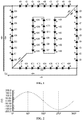
- FIG. 1 depicts a schematic representation of an example AC LED circuit with LEDs configured as a full-wave rectifier and a string of LEDs configured to receive unidirectional current from the rectifier.
- the depicted AC LED is one example of a self rectified LED circuit.
- the rectifier LEDs (depicted on the four sides) conduct current only in two out of four AC quadrants (Q1, Q2, Q3, Q4).
- Load LEDs (depicted diagonally within the rectifier) conduct current in all four quadrants. For example, in Q1 and Q2 when voltage is positive and rising or falling respectively, current is conducted through rectifier LEDs (+D1 to +Dn) and through load LEDs ( ⁇ D1 to ⁇ Dn).
- Q3 and Q4 when voltage is negative and falling or rising respectively, current is conducted through rectifier LEDs (-D1 to -Dn) and through load LEDs ( ⁇ D1 to ⁇ Dn).
- input voltage may have to reach a predetermined conduction angle voltage in order for LEDs to start conducting significant currents.
- Figure 2 depicts a sinusoidal voltage, with one period of excitation spanning four quadrants.
- Q1 spans 0 to 90 degrees (electrical)
- Q2 spans 90 to 180 degrees (electrical)
- Q3 spans 180 to 270 degrees (electrical)
- Q4 spans 270 to 360 (or 0) degrees (electrical).
- Figure 3 depicts an exemplary characteristic curve for an LED.
- the current is depicted as substantially negligible below a threshold voltage of approximately 2.8 volts.
- this particular characteristic is for one LED and may be different for other suitable LEDs, and therefore this specific Figure is not intended to be limiting. This characteristic may vary as a function of temperature.
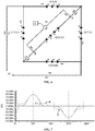
- Figure 4 depicts an illustrative current waveform for the sinusoidal voltage of Figure 2 applied to the circuit of Figure 1 .
- the conduction angle begins at about 30 degrees, as shown, and extends to about 150 degrees electrical.
- the conduction angle extends from about 210 degrees (electrical) to about 330 degrees (electrical). Each half cycle is depicted as conducting current for about only 120 degrees.
- Figure 5 depicts representative variations in the current waveform, for example, in different circuit configurations.
- increased conduction angle (as indicated by curve “a") may be obtained by reducing the number of series LEDs, which may lead to excessive peak currents.
- harmonic reduction (as indicated by curve "b") may be attempted by introducing extra series resistance, which may increase power dissipation and/or reduce light output.
- Method and apparatus described next herein include selective current diversion circuitry, which may advantageously increase conduction angle of the AC LED, and/or improve power factor. Some implementations may further advantageously be arranged to substantially improve a balance of current loading among the load LEDs.
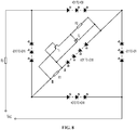
- FIG. 6 depicts a first exemplary embodiment of the full-wave rectifier lighting system with selective current diversion for improved power factor capability.
- the bypass circuit includes a switch SW1 and a sensing circuit SC1.
- the bypass circuit is activated when the SW1 closes to divert current around at least some of the load LEDs.
- the switch SW1 is controlled by the sensing circuit SC1, which selects when to activate the bypass circuit.
- the SC1 operates by sensing input voltage. For example, when the sensed input voltage is below a threshold value, the bypass circuit may be activated to advance the conduction of current in Q1 or Q3, and then to maintain current conduction in Q2 or Q4.
- the SC1 may operate by sensing a current. For example, when the sensed LED current is below a threshold value, the bypass circuit is activated to advance the conduction of current in Q1 or Q3, and then to maintain current conduction in Q2 or Q4.
- the SC1 operates by sensing a voltage derived from the rectified voltage. For example, voltage sensing may be performed using a resistive divider.
- a threshold voltage may be determined by a high value resistor coupled to drive current through an LED of an opto-coupler that controls the state of the SW1.
- the SW1 may be controlled based on a predetermined time delay relative to a specified point in the voltage waveform (e.g., zero crossing or a voltage peak). In such cases the timing may be determined to minimize harmonic distortion of the current waveform supplied from the AC supply to the light apparatus.
- the bypass switch SW1 may be arranged to activate primarily in response to a voltage signal that exceeds a threshold.
- the voltage sensing circuitry may be equipped to switch with a predetermined amount of hysteresis to control dithering near the predetermined threshold.
- some embodiments may further include auxiliary current and/or timing-based switching. For example, if the current exceeds some predetermined threshold value and/or the timing in the cycle is beyond a predetermined threshold, and no signal has yet been received from the voltage sensing circuit, then the bypass circuit may be activated to continue to achieve reduced harmonic distortion.
- the circuit SC1 may be configured to sense input voltage VAC. Output of the SC1 is high (true) when the input voltage is under a certain or predetermined value VSET. The switch SW1 is closed (conducting) if SC1 is high (true). Similarly, the output of the SC1 is low (false) when the voltage is over a certain or predetermined value VSET. The switch SW1 is open (non conducting) if SC1 is low (false). VSET is set to value representing total forward voltage of rectifier LED (+D1 to +Dn) at a set current.
- the sensing circuit SC1 functions similarly on both positive and negative half-cycles in that it may control an impedance state of the SW1 in response to an absolute value of VSET. Accordingly, substantially the same operation occurs in both half-cycles (e.g., Q1-Q2, or Q3-Q4) except load current will be flowing through rectifier LEDs (-D1 to -Dn) during the Q3-Q4.
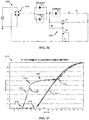
- Figure 7 depicts representative current waveforms with and without use of the bypass circuit path to perform selective current diversion for the circuit of Figure 6 .
- An exemplary characteristic waveform for the input current with the selective current diversion is shown in curves (a) and (b).
- a curve (c) represents an exemplary characteristic waveform for the input current with the selective current diversion disabled (e.g., high impedance in the bypass path).
- a conduction angle for the waveform of curves (a,b) is shown as extending from about 10 - 15 degrees (electrical) to about 165 - 170 degrees (electrical) in Q1, Q2 and about 190 - 195 degrees (electrical) to about 345 - 350 degrees (electrical) in Q3, Q4, respectively.
- the SC1 may operate in response to a sensed current.
- the SC1 may sense current flowing through the rectifier LEDs (+D1 to +Dn) or (-D1 to -Dn), respectively.
- Output of the SC1 is high (true) when the forward current is under a certain preset or predetermined value ISET.
- the switch SW1 is closed (conducting) if SC1 is high (true).
- the output of the SC1 is low (false) when the forward current is over a certain or predetermined value ISET.
- the switch SW1 is open (non conducting) if SC1 is low (false).
- ISET may be set to a value, for example, representing current at a nominal forward voltage of rectifier LEDs (+D1 to +Dn).
- FIG. 8 shows an exemplary embodiment that operates the bypass circuit in response to a bypass circuit responsive to an input current supplied by the excitation source (VAC) through a series resistor R3.
- a resistor R1 is introduced at a first node in series with the load LED string ( ⁇ D1 to ⁇ D18).
- R1 is connected in parallel with a base and emitter of a bipolar junction transistor (BJT) T1, the collector of which is connected to a gate of an N-channel field effect transistor (FET) T2 and a pull-up resistor R2.
- BJT bipolar junction transistor
- FET N-channel field effect transistor
- R2 is connected at its opposite end to a second node on the LED string.
- the drain and source of the transistor T2 are coupled to the first and second nodes of the LED string, respectively.
- the sensing circuit is self biased and there is no need for an external power supply.
- a gate of the transistor T2 may become forward biased and fed through resistor R2, which value may be set to several hundred k ⁇ . Switch T1 will be fully closed (activated) after input voltage reaches approximately 3V. Now current flows through rectifier LEDs (+D1 to +Dn), switch T2 and Resistor R1 (bypass circuit).
- the transistor T1 will tend to reduce a gate-source voltage for the transistor T2, which will tend to raise an impedance of the bypass path.
- the current will transition from the transistor T2 to the load LEDs ( ⁇ D1 to ⁇ Dn) as the input current amplitude increases.
- a similar situation will repeat in a negative half-cycle, except current will flow through rectifier LEDs (-D1 to -Dn) instead.
- load balancing may advantageously reduce the asymmetric duty cycles or substantially equalize duty cycles as between the rectifier LEDs and the load LEDs (e.g., those that carry the unidirectional current in all four quadrants). In some examples, such load balancing may further advantageously substantially reduce flickering effect which is generally lower at LEDs with higher duty cycle.
- Bypass circuit embodiments may include more than one bypass circuit. For example, further improvement of the power factor may be achieved when two or more bypass circuits are used to bypass selected LEDs.
- FIG. 9 shows two bypass circuits.
- SC1 and SC2 may have different thresholds and may be effective in further improving the input current waveform so as to achieve even higher conduction angles.
- the number of bypass circuits for an individual AC LED circuit may, for example, be 1, 2, 3, 4, 5, 6, 7, 8, 9, 10, 11, 12, 13, 14, or more, such as 15, about 18, 20, 22, 24, 26, 28, or at least 30, but may include as many permutations as practicable to improve power quality.
- a bypass circuit may be configured to divert current away from a single LED, or any number of series-, parallel- or series/parallel-connected LEDs as a group, in response to circuit conditions.
- Bypass circuits may be applied to LEDs in the load LEDs, as shown in the example embodiments in Figures 6 , 8 and 10 .
- one or more bypass circuits may be applied to selectively divert current around one or more LEDs in the full-wave rectifier stage.
- bypass circuit can be implemented with a few discrete components.
- a bypass circuit may be manufactured on a single die with the LEDs.
- the bypass circuit may be implemented in whole or in part using discrete components, and/or integrated with one or more LEDs associated with a group of bypassed LEDs or the entire AC LED circuit.
- Figure 10 depicts an example AC LED lighting apparatus that includes two strings of LEDs configured as a half-wave rectifier in which each LED string conducts and illuminates on alternating half cycles.
- a positive group (+D1 to +Dn) conducts current in Q1 and Q2
- a negative group (-D1 to -Dn) conducts current in Q3 and Q4.
- the AC input voltage may have to reach a threshold excitation voltage corresponding to a corresponding conduction angle in order for LEDs to start conducting significant currents, as discussed with reference to Figure 4 .
- Figure 11 depicts a typical sinusoidal excitation voltage Vac waveform for exciting the AC LED lighting apparatus of Figure 10 .
- This waveform is substantially similar to that described with reference to Figure 2 .
- Some of the exemplary methods and apparatus described herein may significantly improve a conduction angle of the AC LED with at least one polarity of a periodically alternating polarity (e.g., sinusoidal AC, triangular wave, square wave) excitation voltage.
- the excitation voltage may be modified by leading and/or trailing phase modulation, pulse width modulation, for example.
- Some examples may achieve advantageous performance improvements with substantially balanced current to the load LEDs.
- the circuit of Figure 10 is modified to include two bypass circuits added across at least some of the load LEDs.
- a first bypass circuit includes a switch SW1 controlled by a sensing circuit SC1.
- a second bypass circuit includes a switch SW2 controlled by a sensing circuit SC2.
- Each bypass circuit provides a bypass path which may be activated and deactivated by switch SW1 or SW2, respectively.
- an exemplary light engine may include 39 LEDs in series for conduction during respective positive and negative half-cycles. It should be understood that any suitable combination of the LEDs in serial and parallel can by used. In various implementations, the number and arrangement of LEDs selected may be a function of the light output, current, and voltage specifications, for example. In some regions the rms line voltage may be about 100V, 120, 200, 220, or 240 Volts.
- the bypass switches are activated in response to input voltage.
- the SC1 may sense input voltage. Output of the SC1 is high (true) when the voltage is under a certain or predetermined value VSET. The SW1 is closed (conducting) if SC1 is high (true). Similarly, the output of the SC1 is low (false) when the voltage is over a certain value or a predetermined threshold VSET. The switch SW1 is open (non conducting) if SC1 is low (false).
- VSET is set, for example, to a value representing total forward voltage, at a set current, of all LEDs outside of the LEDs bypassed by the bypass circuit.
- the same process will repeat when input voltage is negative except load will be flowing through the negative LED group (-D1 to -D30) substantially as described with reference to the positive LED group.
- the sensing circuit SC2 and switch SW2 may be activated or deactivated accordingly as the input voltage reach a negative value of VSET.
- Figure 13 depicts representative current waveforms with and without use of the bypass circuit path to perform selective current diversion for the circuit of Figure 12 .
- An exemplary characteristic waveform for the input current with the selective current diversion is shown in curves (a) and (b).
- a curve (c) represents an exemplary characteristic waveform for the input current with the selective current diversion disabled (e.g., high impedance in the bypass paths).
- the selective current diversion technology of this example may significantly increase a conduction angle, substantially as described with reference to Figure 7 . By bypassing LEDs (+D10 to +D29) and (-D10 to -D29) respectively, conduction angle may be significantly improved.
- the bypass switches SW1, SW2 may be activated in response to input voltage sense signals.
- the SC1, SC2 senses current flowing through LEDs (+D1 to +D9) and (+D30 to +D39) respectively.
- Output of the SC1 is high (true) when the forward current is under a certain value or predetermined threshold ISET.
- the switch SW1 is closed (conducting) if SC1 is high (true).
- the output of the SC1 is low (false) when the forward current exceeds ISET.
- the switch SW1 may transition to an open (non conducting) state while SC1 is low (false).
- ISET may, for example, be set to a value approximately representing current at nominal forward voltage of sum of LED (+D1 to +D9) and (+D30 to +D39).
- load balancing may advantageously reduce flickering effect, if any. Where applicable, flickering effects may be generally reduced by increasing duty cycle and/or conduction angle for the LEDs.
- Bypass circuitry operable to condition current using selective current diversion technology is not limited to embodiments with only one bypass circuit.
- some examples may include an increased number of the bypass circuits and arrange the LEDs into a number of subgroups. Exemplary embodiments with more than one bypass circuit are described with reference at least to Figures 9 , 12 , 20 , 39 , or 42-43 , for example.
- some bypass circuit embodiments can be manufactured on a single die with one or more LEDs in an AC LED light engine.
- Figure 14 depicts an exemplary AC LED topology which includes a conventional diode rectifier feeding a string of LEDs.
- This exemplary topology includes a full bridge rectifier and load LEDs (+D1 to +D39) as shown in Figure 14 .
- Figure 15 shows a sinusoidal voltage after being processed by a full bridge rectifier. Voltage across LEDs (+D1 to +D39) is substantially always uni-directional (e.g., positive) in polarity.
- Figure 16 illustrates a current waveform that illustrates operation of the AC LED circuit of Figure 14 .
- the input voltage has to reach a predetermined conduction angle voltage in order for LEDs to start conducting higher currents.
- This waveform is substantially similar to that described with reference to Figure 4 .
- Figures 17-19 disclose exemplary embodiments that illustrate selective current diversion applied to the AC LED topology of Figure 14 .
- Figure 17 shows a schematic of the AC LED topology of Figure 14 that further includes a bypass circuit applied to a portion of the LEDs in the load.
- Method and apparatus described herein may significantly improve a conduction angle of an AC LED.
- FIG 17 there is an additional exemplary bypass circuit added across the load LEDs.
- the bypass circuit is activated and deactivated by the switch (SW1).
- the switch SW1 is controlled by the sensing circuit SC1.
- the SC1 controls the bypass switch in response to input voltage.
- SC1 may sense input voltage at a node A (see Figure 17 ).
- Output of the SC1 is high (true) when the voltage is under a certain or predetermined value VSET.
- the switch SW1 is closed (conducting) if SC1 is high (true).
- the output of the SC1 is low (false) when the voltage is over a certain or predetermined value VSET.
- the switch SW1 is open (non conducting) if SC1 is low (false).
- VSET is set to a value approximately representing total forward voltage sum of LEDs (+D1 to +D9) and (+D30 to +D39) at a set current.
- Figure 18 shows exemplary effects on the input current. By bypassing group of LEDs (+D11 to +D29), conduction angle may be significantly improved.
- the SC1 controls the bypass switch in response to current sense.
- SC1 is sensing current flowing through LED (+D1 to +D9) and (+D30 to +D39) respectively.
- Output of the SC1 is high (true) when the forward current is under certain or predetermined value ISET.
- Switch SW1 is closed (conducting) if SC1 is high (true).
- the output of the SC1 is low (false) when the forward current is over certain or predetermined value ISET.
- Switch SW1 is open (non conducting) if SC1 is low (false).
- ISET is set to a value representing current at a nominal forward voltage of sum of the LEDs (+D1 to +D9) and (+D30 to +D39).
- Various embodiments may advantageously provide, for a full-wave rectified AC LED light engine, a reduction in flickering effect which may be generally lower for LEDs operated with higher duty cycle.
- Some embodiments may include more than one bypass circuit arranged to divert current around a group of LEDs.
- two or more bypass circuits may be employed.
- two or more bypass circuits may be arranged to divide a group of bypass LEDs into subgroups.
- a light engine embodiment may include at least two bypass circuits arranged to selectively divert current around two separate groups of LEDs (see, e.g., Figures 9 , 26 ).
- Figure 12 shows an example light engine that includes two bypass circuits. Further embodiments of light engine circuits with more than one bypass path are described at least with reference to Figures 42-43 , for example.
- FIG 19 shows an exemplary implementation of a bypass circuit for an LED light engine.
- a bypass circuit 1900 for selectively bypassing a group of LEDs includes a transistor T2 (e.g., n-channel MOSFET) connected in parallel with the LEDs to be bypassed.
- a gate of the transistor T2 is controlled by a pull-up resistor R2 and a bipolar junction transistor T1.
- the transistor T1 is responsive to a voltage across the sense resistor R1, which carries the sum of the instantaneous currents through the transistor T2 and the LEDs.
- Various embodiments may operate light engine by modulating impedance of the transistor T2 at an integral (e.g., 1, 2, 3) multiple of line frequency (e.g., about 50 or 60 Hz).
- the impedance modulation may involve operating the transistor T2 in the bypass path in a linear (e.g., continuous or analog) manner by exercising its saturated, linear, and cut-off regions, for example, over corresponding ranges of circuit conditions (e.g., voltage, current).
- the operating mode of the transistor may be a function of the level of instantaneous input current. Examples of such function will be described with reference to at least Figures 22 , 27 or 32 , for example.
- Figure 20 shows a block diagram of an exemplary apparatus for calibrating or testing power factor improvements in embodiments of the lighting apparatus.
- the apparatus provides capabilities to test the harmonic content of the current, measure power factor for a large number of configurations of bypass switches at independently controlled voltage or current thresholds.
- an automated test procedure for example, may be able to rapidly determine an optimal configuration for one or more bypass switches for any lighting apparatus.
- the resulting optimal configuration may be stored in a database, and/or downloaded to a data store device associated with the lighting apparatus under test.
- the depicted apparatus 2000 includes a rectifier 2005 (which may include LEDs, diodes, or both) in series with a load that includes an auxiliary module of components and a string of LEDs for illumination.
- the apparatus further includes an analog switch matrix 2010 that can connect any node in the diode string to the terminals of any of a number of bypass switches.
- a test pin fixture may be used to make contact with the nodes of the lighting apparatus under test.
- the apparatus further includes a light sensor 2020, which may be configured to monitor the intensity and/or color temperature output by the lighting apparatus.
- the apparatus further includes a controller 2025 that receives power factor (e.g., harmonic distortion) data from a power analyzer 2030, and information from the light sensor 2020, and is programmed to generate control commands to configure the bypass switches.
- power factor e.g., harmonic distortion
- the controller sends a command to connect selected nodes of the lighting apparatus to one or more of the bypass switches.
- the bypass switches may be implemented as relays, reed switches, IGBTs, or other controllable switch element.
- the analog switch matrix 2010 provides for flexible connections from available nodes of the LED string to a number of available bypass switches.
- the controller also sets the threshold conditions at which each of the bypass switches may open or close.
- the controller 2025 may access a program 2040 of executable instructions that, when executed, cause the controller to operate a number of bypass switches to provide a number of combinations of bypass switch arrangements.
- the controller 2025 may execute the program of instructions to receive a predetermined threshold voltage level in association with any or all of the bypass switches.
- the controller 2025 may operate to cause a selected one of the bypass switches to transition between a low impedance state and a dynamic impedance state. In some examples, the controller 2025 may cause a transition when an applied excitation voltage crosses a predetermined threshold voltage. In some examples, the controller 2025 may cause a transition when an input current crosses a predetermined threshold current, and/or satisfies one or more time-based conditions.
- specifications may include power factor, total harmonic distortion, efficiency, light intensity and/or color temperature.
- one or more cost values may be determined (e.g., based on component cost, manufactured cost).
- a lowest cost or optimal output configuration may be identified in a configuration that includes two bypass paths, a set of LEDs to be bypassed by each bypass circuit, and two bypass circuits. Each path may be characterized with a specified impedance characteristic in each bypass circuit.
- Experimental results are described with reference to Figures 21-37 .
- Experimental measurements were collected for a number of illustrative embodiments that included selective current diversion to condition current for an LED light engine.
- the applied excitation voltage was set to a 60 Hz sinusoidal voltage source at 120 Vrms (unless otherwise indicated) using an Agilent 6812B AC Power Source/Analyzer.
- Waveform plots and calculated power quality parameters for the input excitation voltage and current were captured using a Tektronix DP03014 Digital Phospor oscilloscope with a DP03PWR module.
- the experimental excitation voltage amplitude, waveform, and frequency are exemplary, and not to be understood as necessarily limiting.
- FIG 21 shows a schematic of an exemplary circuit for an LED light engine with improved harmonic factor and/or power factor performance.
- a light engine circuit 2100 includes a full wave rectifier 2105 that receives electrical excitation from a periodic voltage source 2110.
- the rectifier 2105 supplies substantially unidirectional output current to a load circuit.
- the load circuit includes a current limiting resistor Rin, a current sense resistor Rsense, a bypass switch 2115 connected to a network of five LED groups (LED Group 1- LED Group 5).
- LED Group 1 and LED Group 2 are two LED networks connected in in a first parallel network.
- LED Group 4 and LED Group 5 are two LED networks connected in a second parallel network.
- LED Group 3 is an LED network connected in series with and between the first and second parallel networks.
- the bypass switch 2115 is connected in parallel with with the LED Group 3.
- a control circuit to operate the bypass switch is not shown, but suitable embodiments will be described in further detail, for example, with reference at least to Figures 6-8 , 19 , or 26-27 .
- the bypass switch 2115 is in a low impedance state at the beginning and end of each period while the AC input excitation current is below a predetermined threshold. While the bypass switch 2115 is in the low impedance state, the input current that flows through the LED Groups 1, 2 is diverted along a path through the bypass switch 2115 that is in parallel to the third group of LEDs. Accordingly, light emitted by the light engine 2100 while the AC input excitation 2110 is below the predetermined threshold is substantially only provided by the LED Groups 1, 2, 4, 5. Engaging the bypass switch 2115 to divert current around the LED Group 3 at low excitation levels may effectively lower the forward threshold voltage needed to begin drawing input current. Accordingly, this substantially increases the conduction angle relative to the same circuit without the bypass switch 2115.
- the bypass switch may exhibit a substantially linearly transition to a high impedance state as the AC input excitation current rises above the predetermined threshold (e.g., the forward threshold voltage of LED Group 3).
- the predetermined threshold e.g., the forward threshold voltage of LED Group 3
- the input current that flows through the first and second groups of LEDs also begins to transition from flowing through the bypass switch 2115 to flowing through the LED Group 3. Accordingly, light emitted by the light engine while the AC input excitation is above the predetermined threshold is substantially a combination of light provided by the LED Groups 1-5.
- the LED Groups 1, 2, 4, 5 may each include about 16 LEDs in series.
- the LED Group 3 may include about 23 LEDs in series.
- the LED Groups 1, 2, 4, 5 may include LEDs that emit a first color output, and the LED Group 3 may include LEDs that emit at least a second color output when driven by a substantial current.
- the number, color, and/or type of LED may be different in and among the various groups of LEDs.
- the first color may be substantially a warm color (e.g., blue or green) with a color temperature of about 2700-3000 K.
- the second color may be substantially a cool color (e.g., white) with a color temperature of about 5000-6000 K.
- Some embodiments may advantageously smoothly transition an exemplary light fixture having an output color from a cool (second) color to a warm (first) color as the AC excitation supplied to the light engine is reduced, for example, by lowering a position of the user input element on the dimmer control. Examples of circuits for providing a color shift are described, for example, with reference to Figures 20A-20C in U.S. Provisional Patent Application serial number 61/234,094 , entitled "Color Temperature Shift Control for Dimmable AC LED Lighting,” filed by Grajcar on 8/14/2009, the entire contents of which are incorporated by reference.
- the LED Groups 1, 2, 4, 5 may each include about eight, nine, or ten LEDs in series, and the LED Group 3 may include about 23, 22, 21, or 20 LEDs, respectively.
- Various embodiments may be arranged with the appropriate resistance and number of series connected diodes to provide, for example, a desired output illumination using an acceptable peak current (e.g., at a peak AC input voltage excitation).
- the LEDs in the LED Groups 1-3 may be implemented as a package or in a single module, or arranged as individual and/or groups of multiple-LED packages.
- the individual LEDs may output all the same color spectrum in some examples. In other examples, one or more of the LEDs may output substantially different colors than the remaining LEDs.
- a parallel arrangement of the LED groups 1, 2, 4, 5 may advantageously substantially reduce an imbalance with respect to aging of the LED Group 3 relative to aging of the LED Groups 1, 2, 4, 5.
- Such an imbalance may arise, for example, where the conduction angle of current through the bypassed LEDs may be substantially less than the conduction angle of current through the first and second groups of LEDs.
- the LED Groups 1, 2, 4, 5 conduct current substantially whenever AC excitation input current is flowing.
- the LED Group 3 only conducts forward current when the bypass bypass switch 2115 is not diverting at least a portion of the input current through a path that is in parallel with the LED Group 3.
- the rectifier bridge 2105 is depicted as a full bridge to rectify single phase AC excitation supplied from the voltage source 2110.
- the rectifier bridge 2105 rectifies both the positive and negative half-cycles of the AC input excitation to produce unidirectional voltage waveform with a fundamental frequency that is twice the input line excitation frequency. Accordingly, some implementations may reduce perceivable flicker, if any, by increasing the frequency at which the LED output illumination pulses.
- half or full wave rectification may be used. In some examples, rectification may operate from more than a single phase source, such as a 3, 4, 5, 6, 9, 12, 15 or more phase source.
- FIGs 22-25 depict experimental results collected by operation of an exemplary LED light engine circuit substantially as shown and described with reference to Figure 21 .
- the LEDs were model CL-L233-MC13L1, commercially available for example from Citizen Electronics Co., Ltd. of Japan.
- the tested LED Groups 1, 2, 4, 5 each included eight diodes in a series string, and LED Group 3 included twenty three diodes in a series string.
- the tested component values were specified as Rin at 500 Ohms and Rsense at 23.2 Ohms.
- Figure 22 shows a graph of normalized input current as a function of excitation voltage for the light engine circuit of Figure 21 .
- a graph 2200 includes a plot 2205 for input current with selective current diversion to condition the current, and a plot 2210 for input current with selective current diversion disabled.
- the plot 2210 may be referred to herein as being associated with resistive conditioning.
- the experimental data shows that, for similar peak current, the effective forward threshold voltage at which substantial conduction begins was reduced from about 85 V (resistive conditioning) at point 2215 to about 40 V (selective current diversion) at a point 2220. This represents a reduction in threshold voltage of over 50%. When applied to both the rising and falling quadrants of each cycle, this corresponds to a substantial expansion of the conduction angle.
- the plot 2205 shows a first inflection point 2220 that, in some examples, may be a function of the LED Groups 1, 2, 4, 5.
- the voltage at the inflection point 2220 may be determined based on the forward threshold voltage of the LED Groups 1, 2, 4, 5, and may further be a function of a forward threshold voltage of the operating branches of the bridge rectifier 2105.
- the plot 2205 further includes a second inflection point 2225.
- the second inflection point 2225 may correspond to a current threshold associated with the bypass control circuit.
- the current threshold may be determined based on, for example, the input current.
- a slope 2230 of the plot 2205 between the points 2220, 2225 indicates, in its reciprocal, that the light engine circuit 2100 with selective current diversion exhibits an impedance in this range that is substantially lower than any impedance exhibited by the plot 2210.
- this reduced impedance effect may advantageously promote enhanced light output by relatively rapidly elevating current at low excitation voltages, where LED current is roughly proportional to light output.
- the plot 2205 further includes a third inflection point 2240.
- the point 2240 may correspond to a threshold above which the current through the bypass switch path is substantially near zero.
- the bypass switch 2115 diverts at least a portion of the input current around the LED Group 3.
- a variable slope shown in a range 2250 of the plot 2205 between the points 2225, 2240 indicates, in its reciprocal, that the bypass switch exhibits in this range a smoothly and continuously increasing impedance in response to increasing excitation voltage.
- this dynamic impedance effect may advantageously promote a smooth, substantially linear (e.g., low harmonic distortion) transition from the current flowing substantially only through the bypass switch 2115 to flowing substantially only in the LED Group 3.
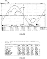
- Figure 23 depicts oscilloscope measurements of voltage and current waveforms for an embodiment of the circuit of Figure 21 .
- a plot 2300 depicts a sinusoidal voltage waveform 2305 and a current waveform 2310.
- the current waveform 2310 exhibits a head-and-shoulders shape.
- a shoulder 2315 corresponds to current that flows through the bypass switch within a range of lower AC input excitation levels. Over a second intermediate range of AC input excitation levels, an impedance of the bypass current increases. As the excitation voltage continues to rise substantially smoothly and continuously within a third range that overlaps with the second range, a voltage across the bypass switch increases beyond an effective forward threshold voltage of the LED Group 3, and the input current transitions in a substantially smooth and continuous manner from flowing in the bypass switch 2115 to flowing through the LED Group 3. At higher AC input excitation levels, the current flows substantially only through the LED Group 3 instead of the bypass switch 2115.
- the first range may have a lower limit that is a function of an effective forward threshold voltage of the network formed by the LED Groups 1, 2, 4, 5.
- the second range may have a lower limit defined by a predetermined threshold voltage.
- the lower limit of the second range may correspond substantially to a predetermined threshold current.
- the predetermined threshold current may be a function of a junction temperature (e.g., a base-emitter junction forward threshold voltage).
- a lower limit of the third range may be a function of an effective forward threshold voltage of the LED Group 3.
- an upper limit of the third range may correspond to the input current flowing substantially primarily (e.g., at least about 90%, 91%, 92%, 93%, 94%, 95%, 96%, 97%, 98%, 99%, or at least about 99.5% of the instantaneous input current to the load) through the LED Group 3.
- the upper limit of the third range may be a function of the current flow through the bypass switch 2115 being substantially near zero (e.g., less than 0.5%, 1%, 2%, 3%, 4%, 5%, 6%, 7%, 8%, 9%, or less than about 10% of the instantaneous input current to the load).
- Figure 24 depicts power quality measurements for the voltage and current waveforms of Figure 23 .
- the measurements indicate that the power factor was measured to be about 0.987 (e.g., 98.7%).
- Figure 25 depicts a harmonic profile for the voltage and current waveforms of Figure 23 .
- the measured total harmonic distortion was measured at about 16.1%.
- embodiments of an LED light engine with selective diversion circuitry may advantageously operate with a power factor substantially above 90%, 92.5%, 95%, 97.5%, or at least above about 98%, for example, and simultaneously achieve a THD substantially below 25%, 22.5%, 20%, or about 18%, for example, at the rated excitation voltage.
- Some embodiments of the AC LED light engine may further be substantially smoothly and continuously dimmable over a full range (e.g., 0-100%) of the applied excitation voltage under amplitude modulation and/or phase controlled modulation.
- Figure 26 shows a schematic of an exemplary circuit for an LED light engine with improved harmonic factor and/or power factor performance.
- Various embodiments may advantageously yield improved power factor and/or a reduced harmonic distortion for a given peak illumination output from the LEDs.
- the light engine circuit 2600 includes a bridge rectifier 2605 and two parallel-connected groups of LEDs: LED Group 1 and LED Group 2, each containing multiple LEDs, and each connected between a node A and a node C.
- the circuit 2600 further includes an LED Group 3 connected between the node C and a node B.
- each of the LED Groups 1, 2, 3 may have an effective forward voltage that is a substantial fraction of the applied peak excitation voltage. Their combined forward voltage in combination with a current limiting element may control the peak forward current.
- the current limiting element is depicted as a resistor R1.
- the current limiting element may include, for example, one or more elements in a combination, the elements being selected from among a fixed resistor, current controlled semiconductor, and a temperature-sensitive resistor.
- the light engine circuit 2600 further includes a bypass circuit 2610 that operates to reduce the effective forward turn-on voltage of the circuit 2600.
- the bypass circuit 2610 may contribute to expanding the conduction angle at low AC input excitation levels, which may tend to benefit power factor and/or harmonic factor, e.g., by constructing a more sinusoidally-shaped current waveform.
- the bypass circuit 2610 includes a bypass transistor Q1 (e.g., metal oxide semiconductor (MOS) field effect transistor (FET), IGBT (insulated gate bipolar transistor), bipolar junction transistor (BJT), or the like) with its channel connected to divert current from the node C and around the LED Group 3 and the series resistor R1.
- MOS metal oxide semiconductor
- FET field effect transistor
- IGBT insulated gate bipolar transistor
- BJT bipolar junction transistor
- the conductivity of the channel is modulated by a control terminal (e.g., gate of the MOSFET).
- the gate of the n-channel MOSFET Q1 is pulled up in voltage through a resistor R2 to the node C. In some other embodiments, the resistor may be pulled up to the node A.
- the gate voltage can be reduced by a pull down transistor Q2 (e.g., MOSFET, IGBT, junction FET (JFET), bipolar junction transistor (BJT), or the like) to a voltage near a voltage of the source of the transistor Q1.
- a pull down transistor Q2 e.g., MOSFET, IGBT, junction FET (JFET), bipolar junction transistor (BJT), or the like
- a collector of the transistor Q2 NPN bipolar junction transistor (BJT)
- a sense resistor R3 is connected across the base-emitter of the transistor Q2.
- the voltage on the gate of the transistor Q1 may be substantially smoothly and continuously varied in response to corresponding smooth and continuous variations in the input current magnitude.
- FIGS 27-29 and 36-37 depict experimental results collected by operation of an exemplary LED light engine circuit substantially as shown and described with reference to Figure 26 .
- the LED Groups 1, 2 were model EHP_A21_GT46H (white), commercially available for example from Everlight Electronics Co., LTD. of Taiwan.
- the LED Group 3 included model EHP_A21_UB 01H (blue), also commercially available for example from Everlight Electronics Co., LTD. of Taiwan.
- the tested LED Groups 1, 2 each included twenty-four diodes in a series string, and the LED Group 3 included twenty-one diodes in a series string.
- the tested component values were specified as R1 at 13.4 Ohms, R2 at 4.2 Ohms, and R3 at 806 kOhms.
- Figure 27 shows a graph of normalized input current as a function of excitation voltage for the light engine circuit of Figure 26 .
- a graph 2700 includes a plot 2705 for input current with selective current diversion to condition the current, and a plot 2710 for input current with selective current diversion disabled.
- the plot 2710 may be referred to herein as being associated with resistive conditioning.
- the experimental data shows that, for a similar peak current, the effective forward threshold voltage at which substantial conduction begins was reduced from about 85 V (resistive conditioning) at point 2715 to about 45 V (selective current diversion) at a point 2720. This represents a reduction in threshold voltage of about 45%. When applied to both the rising and falling quadrants of each rectified sinusoid cycle, this corresponds to a substantial expansion of the conduction angle.
- the plot 2705 shows the first inflection point 2720 that, in some examples, may be a function of the LED Groups 1, 2.
- the voltage at the inflection point 2720 may be determined based on the forward threshold voltage of the LED Groups 1, 2, and may further be a function of a forward threshold voltage of the operating branches of the bridge rectifier 2605.
- the plot 2705 further includes a second inflection point 2725.
- the second inflection point 2725 may correspond to a current threshold associated with the bypass circuit 2610.
- the current threshold may be determined based on, for example, the input current, base-emitter junction voltage, temperature, current gain, and/or the transfer characteristics for the transistor Q1.
- a slope 2730 of the plot 2705 between the points 2720, 2725 indicates, in its reciprocal, that the light engine circuit 2600 with selective current diversion exhibits an impedance in this range that is substantially lower than any impedance exhibited by the plot 2710.
- this reduced impedance effect may advantageously promote, for example, enhanced light output by relatively rapidly elevating current at low excitation voltages, where LED current is roughly proportional to light output.
- the plot 2705 further includes a third inflection point 2740.
- the point 2740 may correspond to a threshold above which the current through the transistor Q1 is substantially near zero. Below the point 2740, the transistor Q1 diverts at least a portion of the input current around the LED Group 3.
- a variable slope shown in a range 2750 of the plot 2705 between the points 2725, 2740 indicates, in its reciprocal, that the transistor Q1 exhibits in this range a smoothly and continuously increasing impedance in response to increasing excitation voltage.
- this dynamic impedance effect may advantageously promote a smooth, substantially linear (e.g., low harmonic distortion) transition from the current flowing substantially only through the transistor Q1 to flowing substantially only in the LED Group 3.
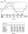
- Figure 28 depicts oscilloscope measurements of voltage and current waveforms for an embodiment of the circuit of Figure 26 .
- a plot 2800 depicts a sinusoidal voltage waveform 2805 and a current waveform 2810.
- the current waveform 2810 exhibits a head-and-shoulders shape.
- shoulders 2815 correspond to current that flows through the transistor Q1 within a range of lower AC input excitation levels.
- an impedance of the transistor Q1 increases.
- a voltage across the transistor Q1 increases beyond an effective forward threshold voltage of the LED Group 3, and the input current transitions in a substantially smooth and continuous manner from flowing in the transistor Q1 to flowing through the LED Group 3.
- the current flows substantially only through the LED Group 3 instead of the transistor Q1.
- the first range may have a lower limit that is a function of an effective forward threshold voltage of the network formed by the LED Groups 1, 2.
- the second range may have a lower limit defined by a predetermined threshold voltage.
- the lower limit of the second range may correspond substantially to a predetermined threshold current.
- the predetermined threshold current may be a function of a junction temperature (e.g., a base-emitter junction forward threshold voltage).
- a lower limit of the third range may be a function of an effective forward threshold voltage of the LED Group 3.
- an upper limit of the third range may correspond to the input current flowing substantially primarily (e.g., at least about 95%, 96%, 97%, 98%, 99%, or at least about 99.5% of the instantaneous input current to the load) through the LED Group 3.
- the upper limit of the third range may be a function of the current flow through the transistor Q1 being substantially near zero (e.g., less than 0.5%, 1%, 2%, 3%, 4%, or less than about 5% of the instantaneous input current to the load).
- Figure 29 depicts power quality measurements for the voltage and current waveforms of Figure 28 .
- the measurements indicate that the power factor was measured to be about 0.967 (e.g., 96.7%).
- FIGs 30-31 depict experimental results collected by operation of an exemplary LED light engine circuit substantially as shown and described with reference to Figure 26 .
- the LED Groups 1, 2, 3 included model SLHNNWW629T0, commercially available for example from Samsung LED Co, LTD. of Korea.
- the LED Group 3 further included model AV02-0232EN, commercially available for example from Avago Technologies of California.
- the tested LED Groups 1, 2 each included twenty-four diodes in a series string, and the LED Group 3 included eighteen diodes in a series string.
- the tested component values were specified as R1 at 47 Ohms, R2 at 3.32 Ohms, and R3 at 806 kOhms.
- Figure 30 depicts oscilloscope measurements of voltage and current waveforms for another embodiment of the circuit of Figure 26 .
- a plot 3000 depicts a sinusoidal excitation voltage waveform 3005 and a plot of an input current waveform 3010.
- the current waveform 3010 exhibits a head-and-shoulders shape, substantially as described with reference to Figure 28 , with modified characteristic thresholds, inflection points, or slopes.
- Figure 31 depicts power quality measurements for the voltage and current waveforms of Figure 30 .
- the measurements indicate that the power factor was measured to be about 0.978 (e.g., 97.8%).
- Figures 32-35 depict experimental results collected by operation of an exemplary LED light engine circuit substantially as shown and described with reference to Figure 26 .
- the LED Groups 1, 2 included model SLHNNWW629T0 (white), commercially available for example from Samsung LED Co, LTD. of Korea, and model AV02-0232EN (red), commercially available for example from Avago Technologies of California.
- the LED Group 3 included model CL-824-U1D (white), commercially available for example from Citizen Electronics Co., Ltd. of Japan.
- the tested LED Groups 1, 2 each included twenty-four diodes in a series string, and the LED Group 3 included twenty diodes in a series string.
- the tested component values were specified as R1 at 715 Ohms, R2 at 23.2 Ohms, and R3 at 806 kOhms.
- Figure 32 show oscilloscope measurements of voltage and current waveforms for the embodiment of the circuit of Figure 26 as described with reference to Figures 27-29 .
- a graph 3200 includes sinusoidal excitation voltage waveform 3205, an total input current waveform 3210, a waveform 3215 for current through the transistor Q1, and a waveform 3220 for current through the LED Group 3.
- the experimental data suggests that for excitation voltages within between the first inflection point 2720 and the second inflection point 2725, the total input current waveform 3210 substantially matches the waveform 3215.
- the input current and current through the transistor Q1 remain substantially equal over a range of excitations above the second inflection point 2725.
- the waveform 3215 begins to decrease at a rate that is substantially offset by a corresponding increase in the waveform 3220.
- the waveforms 3215, 3220 appear to have equal and opposite, approximately constant (e.g., linear) slope as the excitation voltage rises voltage corresponding to the inflection point 3225 to the voltage corresponding to the inflection point 2740.
- the waveform 3220 for current through the LED Group 3 substantially equals the input current waveform 3210.
- Figure 33 depicts power quality measurements for the voltage and current waveforms of Figure 32 .
- the measurements indicate that the power factor was measured to be about 0.979 (e.g., 97.9%).
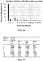
- Figure 34 depicts a harmonic components for the waveforms of Figure 32 .
- the harmonic magnitudes were measured substantially only as odd harmonics, the strongest being a 7th harmonic at less than 20% of the fundamental.
- Figure 35 depicts a harmonic profile for the voltage and current waveforms of Figure 32 .
- the measured total harmonic distortion was measured at about 20.9%.
- embodiments of an AC LED light engine with selective diversion circuitry may advantageously operate with less than 30%, 29%, 28%, 27%, 26%, 25%, 24%, 23%, 22%, or less than about 21% THD, and where the magnitudes of the harmonics at frequencies above one kHz, for example, are substantially less than about 5% of the amplitude of the fundamental frequency.
- Figures 36-37 shows a plot and data for experimental measurements of light output for a light engine as described with reference to Figure 27 .
- the light output was measured to exhibit about a 20% optical loss associated with a lens and a white-colored (e.g., substantially parabolic) reflector.
- the measured input power was 14.41 Watts.
- embodiments of an AC LED light engine with selective diversion circuitry may advantageously operate with at least about 42, 44, 46, 48, 50, or about 51 lumens per watt, and with a power factor of at least 90%, 91%, 92%, 93%, 94%, 95%, or at least 96% when supplied with about 120 Vrms sinusoidal excitation.
- Some embodiments of the AC LED light engine may further be substantially smoothly and continuously dimmable over a full range (e.g., 0-100%) of the applied excitation voltage under amplitude modulation and/or phase controlled modulation.
- Figure 36 shows a graph of calculated components of the light output, and the combined total output calculation, at a range of dimming levels.
- the graph indicates that the selective diversion circuitry in this implementation provides a smoothly dimmable light output over a substantial voltage range.
- the light output was smoothly (e.g., continuous, monotonic variation) reduced from 100% at full rated excitation (e.g., 120 V in this example) to 0% at about 37% of rated excitation (e.g., 45 V in this example).
- a usable control range for smooth dimming using amplitude modulation of some implementation of an AC LED light engine with selective current diversion to condition the current may be at least 60% or at least about 63% of the rated excitation voltage.
- Figure 37 shows experimental data for the calculated components of the light output, and the combined total output calculation, at a range of dimming levels.
- the LED Groups 1, 2 output light of at least 5 lumens down to below 50 Volts, and the LED Group 3 output light of at least 5 lumens down to about 90 Volts.
- Figure 38 shows a schematic of an exemplary circuit for an LED light engine with selective current diversion to bypass a group of LEDs while AC input excitation is below a predetermined level.
- Various embodiments may advantageously yield improved power factor and/or a reduced harmonic distortion for a given peak illumination output from the LEDs.
- the light engine circuit 3800 includes a bridge rectifier 3805 and two series-connected groups of LEDs: LED Group 1 and LED Group 2, each containing multiple LEDs.
- each of the LED Group 1, 2 may have an effective forward voltage that is a substantial fraction of the applied peak excitation voltage. Their combined forward voltage in combination with a current limiting element may control the peak forward current.
- the current limiting element is depicted as resistor R1.
- the current limiting element may include, for example, one or more elements in a combination, the elements being selected from among a fixed resistor, current controlled semiconductor, and a temperature-sensitive resistor.
- the light engine circuit 3800 further includes a bypass circuit 3810 that operates to reduce the effective forward turn-on voltage of the circuit 3800.
- the bypass circuit 3810 may contribute to expanding the conduction angle at low AC input excitation levels, which may tend to benefit power factor and/or harmonic factor, e.g., by constructing a more sinusoidally-shaped current waveform.
- the bypass circuit 3810 includes a bypass transistor Q1 (e.g., MOSFET, IGBT, bipolar, or the like) with its channel connected in parallel with the LED Group 2.
- the conductivity of the channel is modulated by a control terminal (e.g., gate of the MOSFET).
- the gate is pulled up in voltage through a resistor R2 to a positive output terminal (node A) of the rectifier, but can be pulled down to a voltage near a voltage of the source of the transistor Q1 by a collector of an NPN transistor Q2.
- the voltage on the gate of the transistor Q1 may be substantially smoothly and continuously varied in response to corresponding smooth and continuous variations in the input current magnitude, which flows through sense resistor R3.
- the NPN transistor Q2 may pull down the gate voltage of the transistor Q1 when a base-emitter of the NPN transistor Q2 is forward biased by sufficient LED current through a sense resistor R3.
- the depicted example further includes an exemplary protection element to limit the gate-to-source voltage of the MOSFET.
- a zener diode 3815 e.g., 14V breakdown voltage
- Figure 39 depicts a schematic of an exemplary circuit for an LED light engine with selective current diversion to bypass two groups of LEDs while AC input excitation is below two corresponding predetermined levels.
- a light engine circuit 3900 includes an additional group of LEDs and a corresponding additional bypass circuit in a series arrangement with the light engine circuit of Figure 38 .
- the light engine circuit 3900 includes an LED Group 1 connected between a node A and a node C, an LED Group 2 connected between the node C and a node D, and an LED Group 3 connected between the node D and a node B in series with LED Groups 1,2.
- the bypass circuits 3905, 3910 include pull-up resistors R2, R4 connected to pull their respective gate voltages up to the nodes C, D, respectively.
- the pull-up resistors R2, R4 may be connected to pull up their respective gate voltages to the nodes A, C, respectively.
- setting appropriate current and voltage thresholds for each of the bypass circuits 3905, 3910 may yield improved performance in terms of at least THD and power factor, taken separately or in combination, in an AC LED light engine such as the light engine 3900.
- one of the bypass circuits may transition from low to high impedance over a first range of excitation, and the other bypass circuit may transition from low to high impedance over a second range of excitation.
- the respective voltage and current thresholds for each of the respective bypass circuits may be set so that the first and second ranges of excitation at least partially overlap. Such overlapping ranges of excitation may be arranged by appropriate selection of current and voltage thresholds to yield, for example an optimal THD performance with improved power factor.
- the first and second ranges of excitation may have substantially no overlap, which may advantageously promote a wider conduction angle, for example, to achieve near unity (e.g., about 97%, 98%, 98.5%, 99%, 99.25%, 99.5%, or about 99.75%) power factor, for example.
- Various embodiments may advantageously provide for two, three, or more bypass circuits, for example, to permit additional degrees of freedom in constructing a more sinusoidally-shaped current waveform, and/or expanding the conduction angle closer to 180 degrees per half-cycle. Additional circuits may introduce additional degrees of freedom, which in turn may yield further improvements to power factor and further reductions in harmonic distortion for a given peak illumination output from the LEDs.
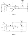
- Figure 40 shows a schematic of an exemplary circuit for an LED light engine with selective current diversion to bypass a group of LEDs while AC input excitation is below a predetermined level.
- the schematic depicted in Figure 40 includes one embodiment of a bridge rectifier 4005, a current limiting resistor R1, and two parallel LED paths, one of which is interruptible by a bypass circuit 4010.
- the light engine circuit 4000 includes the bridge rectifier 4005, which supplies a unidirectional load current through a resistor R1.
- the load current flows through a sense resistor R2 to two parallel groups of LEDs: LED Group 1 and LED Group 2, each formed of multiple LEDs (e.g., arranged in series, parallel, or combined series-parallel network).
- the load current also supplies to the bypass circuit 4010 a bias current that may flow around the LED Groups 1, 2.
- the bypass circuit 4010 includes a P-channel MOSFET transistor Q1 in series with the current path through the LED Group 2.
- the transistor Q1 is connected so that a drain current flows from the resistor R2 to the LED Group 2.
- a voltage of a gate of the transistor Q1 is controlled by a PNP bipolar junction transistor Q2 with it's base-emitter voltage controlled in response to the load current to the LED Groups 1,2 through the sense resistor R2.
- a collector current flowing in response to the load current through the resistor R2 results in a collector current through the transistor Q2 and a bias resistor R3.
- the gate voltage is a function of the voltage across the resistor R3. As the collector current increases, for example, the gate voltage rises.
- the gate voltage increases correspond to a smooth transition in the transistor Q1 from a substantially low impedance state (e.g., less than 100, 50, 30, 20, 10, 5. 1, 0.5, 0.1, 0.05 Ohms), to an increasing impedance state (e.g., equivalent circuit of a substantially constant current source in parallel with a resistance), to a high impedance state (e.g., substantially open circuit).
- Each of the LED Groups 1, 2 may have an effective forward voltage that is a fraction of the applied peak excitation voltage, and substantially all the load current may be divided among the LED Groups 1, 2.
- the applied excitation voltage is sufficient to overcome the effective forward threshold voltage of the LED Group 1, then the load current through the resistor R2 will increase in response to the current flow through the LED Group 1.
- the current flow through the LED Group 2 may decrease substantially smoothly and continuously in response to the current through the sense resistor substantially smoothly and continuously increasing within a range. In some implementations, this range may correspond to an excitation voltage substantially above the effective forward threshold voltage of the LED Group 1.
- the LED Group 2 may have a substantially lower effective forward threshold voltage than the LED Group 1.
- the load current may flow first through LED Group 1.
- the load current flows through both LED Groups 1, 2.
- the current through the LED Group 2 may smoothly and continuously transition toward zero as the bypass circuit 4010 increases an impedance of the channel of the transistor Q1.
- the load current flows substantially only through the LED Group 1, with a small fraction of the load current supplying the bias current to the transistor Q2 in the bypass circuit 4010.
- the light engine circuit 4000 thus includes a bypass circuit 4010 that operates to reduce the effective forward turn-on voltage of the circuit 4000.
- the bypass circuit 4010 may contribute to expanding the conduction angle at low AC input excitation levels, which may tend to benefit power factor and/or harmonic factor, e.g., by constructing a more sinusoidally-shaped current waveform.
- Figure 41 shows a schematic of an exemplary circuit for the LED light engine of Figure 40 with an additional LED group in a series arrangement.
- the light engine circuit 4000 is modified to include an LED Group 3 connected in series with the series resistor R1.
- the LED Group 3 may increase the effective forward threshold voltage requirement for the LED Groups 1, 2.
- some embodiments may provide that the LED Group 3 is illuminating when the LED Group 1 is illuminating at low excitation levels, when the LED Groups 1, 2 are illuminating at intermediate excitation levels, and when the LED Group 2 is illuminating and the LED Group 1 is not illuminating at higher excitation levels.
- some embodiments may use different colors in the LED Group 1 and LED Group 2 to provide substantially different composite color temperatures as a function of excitation level (e.g., color shifts in response to dimming level within a range of 0-100% of rated voltage). Some embodiments may achieve a desired color shift capability by appropriate selection of spectral output for each of the LED Groups 1, 2, and 3.
- Figure 42 shows a schematic of another exemplary circuit for an LED light engine with selective current diversion to bypass a group of LEDs while AC input excitation is below a predetermined level.
- the schematic depicted in Figure 42 includes one embodiment of a light engine circuit that includes a bridge rectifier 4205, current limiting resistor R1, and three parallel LED paths, two of which are interruptible by independent bypass circuits, substantially as described above with reference to Figure 40 .
- the schematic of Figure 42 includes the elements of the light engine circuit 4000 of Figure 40 , and further includes a third parallel path that includes an LED Group 3 that is interruptible by a bypass circuit 4210.
- the bypass circuits 4010, 4210 include a p-channel MOSFET Q1, Q2, respectively, as the bypass transistor.
- a gate of each of the the bypass transistors Q1, Q2 is controlled by a PNP type bipolar junction transistor Q3, Q4.
- the PNP transistors Q3, Q4 are arranged to respond to current through two current sense resistors R2, R3.
- the bypass circuit 4210 for the LED Group 3 turns off at a lower excitation threshold than the corresponding threshold at which the LEDs2 turns off.
- Figure 43 show a schematic of a further exemplary circuit for an LED light engine with selective current diversion to bypass a group of LEDs while AC input excitation is below a predetermined level.
- the schematic depicted in Figure 43 includes one embodiment of a light engine circuit substantially as described above with reference to Figure 42 , and further includes an additional LED group substantially as described with reference to Figure 41 .
- Figure 43 shows a schematic of an exemplary circuit for the LED light engine of Figure 42 with an additional LED group in a series arrangement.
- the light engine circuit 4200 is modified to include an LED Group 4 connected in series with the series resistor R1.
- the LED Group 4 may increase the effective forward threshold voltage requirement for the LED Groups 1, 2, and 3.
- bypass circuits implementations may be controlled in response to signals from analog or digital components, which may be discrete, integrated, or a combination of each.
- Some embodiments may include programmed and/or programmable devices (e.g., PLAs, PLDs, ASICs, microcontroller, microprocessor), and may include one or more data stores (e.g., cell, register, block, page) that provide single or multi-level digital data storage capability, and which may be volatile and/or non-volatile.
- Some control functions may be implemented in hardware, software, firmware, or a combination of any of them.
- Computer program products may contain a set of instructions that, when executed by a processor device, cause the processor to perform prescribed functions. These functions may be performed in conjunction with controlled devices in operable communication with the processor.
- Computer program products which may include software, may be stored in a data store tangibly embedded on a storage medium, such as an electronic, magnetic, or rotating storage device, and may be fixed or removable (e.g., hard disk, floppy disk, thumb drive, CD, DVD).
- the number of LEDs in each of the various embodiments is exemplary, and is not meant as limiting.
- the number of LEDs may be designed according to the forward voltage drop of the selected LEDs and the applied excitation amplitude supplied from the source. With reference to Figure 26 , for example, the number of LEDs in the LED Groups 1, 2 between nodes A, C may be reduced to achieve an improved power factor.
- the LEDs between nodes A, C may be advantageously placed in parallel to substantially balance the loading of the two sets of LEDs according to their relative duty cycle, for example, with respect to the loading of the LED Group 3.
- current may flow from node A to C whenever input current is being drawn from the source, while the current between nodes C and B may flow substantially only around peak excitation.
- apparatus and methods may advantageously improve power factor without introducing substantial resistive dissipation in series with the LED string.
- one or more of the LEDs in the lighting apparatus may have different colors and/or electrical characteristics.
- the rectifier LEDs (which carry current only during alternating half cycles) of the embodiment of Figure 6 may have a different color temperature than the load LEDs that carry the current during all four quadrants.
- additional components may be included, for example, to reduce reverse leakage current through the diodes.
- a low reverse leakage rectifier that is not an LED may be included in series with both branches of the rectifier to minimize reverse leakage in the positive and negative current paths in the rectifier.
- AC input to the rectifier may be modified by other power processing circuitry.
- a dimmer module that uses phase-control to delay turn on and/or interrupt current flow at selected points in each half cycle may be used.
- harmonic improvement may still advantageously be achieved even when current is distorted by the dimmer module.
- Improved power factor may also be achieved where the rectified sinusoidal voltage waveform is amplitude modulated by a dimmer module, variable transformer, or rheostat, for example.
- the excitation voltage may have a substantially sinusoidal waveform, such as line voltage at about 120VAC at 50 or 60 Hz.
- the excitation voltage may be a substantially sinusoidal waveform that has been processed by a dimming circuit, such as a phase-controlled switch that operates to delay turn on or to interrupt turn off at a selected phase in each half cycle.
- the dimmer may modulate the amplitude of the AC sinusoidal voltage (e.g., AC-to-AC converter), or modulate the rectified sinusoidal waveform (e.g., DC-to-DC converter).
- Line frequencies may include about 50, about 60, about 100, or about 400 Hz, for example.
- the fundamental operating frequency may be substantially below 1 kHz, which may advantageously reduce problems with exceeding permissible radio frequency emissions which may be associated with harmonic currents.
- the substantially smooth linear waveforms during operation may advantageously yield substantially negligible harmonic levels.
- Some examples may emit conducted or radiated emissions at such low levels and at such low frequencies that they may be considered to be substantially negligible in the audio or RF range.
- Some embodiments may require substantially no filtering components to meet widely applicable standards that may typically govern conducted or radiated electromagnetic emissions, such as those that may apply to residential or commercial lighting products.
- various embodiments may advantageously operate in residential or commercial applications without filter components, such as capacitors (e.g., aluminum electrolytic), inductors, chokes, or magnetic or electric field absorption or shielding materials. Accordingly, such embodiments may advantageously provide high efficiency, dimmable lighting without the cost, weight, packaging, hazardous substances, and volume associated with such filter components.
- bypass circuitry may be manufactured on a single die integrated with some or all of the illuminating LED.
- an AC LED module may include a die that includes one or more of the LEDs in the group that is to be bypassed, and may further include some or all of the bypass circuit components and interconnections.
- Such implementations may substantially further reduce assembly and component cost by reducing or substantially eliminating placement and wiring associated with embodiments of the bypass circuit.
- integration of the bypass circuitry with the LEDs on the same die or hybrid circuit assembly may eliminate at least one wire or one interface electrical connection.
- the electrical interface between the bypass circuit and the LED on separate substrates may involve a wire or other interconnect (e.g., board-to-board header) to permit current diversion to the bypass circuit and away from the LEDs to be bypassed.
- a wire or other interconnect e.g., board-to-board header
- the space for component placement and/or interconnect routing for the bypass path may be substantially reduced or eliminated, further fostering cost reductions and miniaturization of a complete AC LED light engine.
- conduction angle refers to the portion (as measured in degrees) of a (180 degrees for a half-cycle) of a rectified sinusoidal waveform during which substantial excitation input current flows into one or more of the LEDs in the load to cause the LEDs to emit light.
- a resistive load may have a 180 degree conduction angle.
- a typical LED load may exhibit a conduction angle less than 180 degrees due to the forward turn-on voltage of each diode.
- the AC input may be excited with, for example, a nominally 120 Volt sinusoidal voltage at 60 Hz, but it is not limited to this particular voltage, waveform, or frequency.
- some implementations may operate with AC input excitation of 115 Volts square wave at 400 Hz.
- the excitation may be substantially unipolar (rectified) sinusoidal, rectangular, triangular or trapezoidal periodic waveforms, for example.
- the peak voltage of the AC excitation may be about 46, 50, 55, 60, 65, 70, 80, 90, 100, 110, 115, 120, 125, 130, 140, 150, 160, 170, 180, 190, 200, 210, 220, 230, 240, 260, 280, 300, 350, 400, 500, 600, 800, 1000, 1100, 1300, or at least about 1500 Volts.
- An exemplary dimmer module may operate in response to user input via a sliding control, which may be coupled to a potentiometer.
- the user control input may be augmented or replaced with one or more other inputs.
- the AC excitation supplied to the light engine may be modulated in response to automatically generated analog and/or digital inputs, alone or in combination with input from a user.
- a programmable controller may supply a control signal to establish an operating point for the dimmer control module.
- An exemplary dimmer module may include a phase control module to control what portion of the AC excitation waveform is substantially blocked from supply to terminals of an exemplary light engine circuit.
- the AC excitation may be modulated using one or more other techniques, either alone or in combination. For example, pulse-width modulation, alone or in combination with phase control, may be used to module the AC excitation at modulation frequency that is substantially higher than the fundamental AC excitation frequency.
- modulation of the AC excitation signal may involve a deenergized mode in which substantially no excitation is applied to the light engine.
- some implementations may include a disconnect switch (e.g., solid state or mechanical relay) in combination with the excitation modulation control (e.g., phase control module).
- the disconnect switch may be arranged in series to interrupt the supply connection of AC excitation to the light engine.
- a disconnect switch may be provided on a circuit breaker panel that receives AC input from an electrical utility source and distributes the AC excitation to the dimmer module.
- the disconnect switch may be arranged at a different node in the circuit than the node in the circuit breaker panel.
- Some examples may include the disconnect switch arranged to respond to an automated input signal (e.g., from a programmable controller) and/or to a user input element being placed into a predetermined position (e.g., moved to an end of travel position, pushed in to engage a switch, or the like).
- an automated input signal e.g., from a programmable controller
- a user input element being placed into a predetermined position (e.g., moved to an end of travel position, pushed in to engage a switch, or the like).
- Some embodiments may provide a desired intensity and one or more corresponding color shift characteristics. Some embodiments may substantially reduce cost, size, component count, weight, reliability, and efficiency of a dimmable LED light source.
- the selective current diversion circuitry may operate with reduced harmonic distortion and/or power factor on the AC input current waveform using, for example, very simple, low cost, and low power circuitry. Accordingly, some embodiments may reduce energy requirements for illumination, provide desired illumination intensity and color over a biological cycle using a simple dimmer control, and avoid illumination with undesired wavelengths. Some embodiments may advantageously be enclosed in a water-resistant housing to permit cleaning using pressurized cold water sprays.
- the housing may be ruggedized, require low cost for materials and assembly, and provide substantial heat sinking to the LED light engine during operation.
- Various examples may include a lens to supply a substantially uniform and/or directed illumination pattern.
- Some embodiments may provide simple and low cost installation configurations that may include simple connection to a drop cord.
- the additional circuitry to achieve substantially reduced harmonic distortion may include a single transistor, or may further include a second transistor and a current sense element.
- a current sensor may include a resistive element through which a portion of an LED current flows.
- significant size and manufacturing cost reductions may be achieved by integrating the harmonic improvement circuitry on a die with one or more LEDs controlled by harmonic improvement circuitry.
- harmonic improvement circuitry may be integrated with corresponding controlled LEDs on a common die without increasing the number of process steps required to manufacture the LEDs alone.
- harmonic distortion of AC input current may be substantially improved for AC-driven LED loads, for example, using either half-wave or full-wave rectification.
- a screw type socket which may sometimes be referred to as an "Edison-screw” style socket
- other types of sockets may be used.
- Some implementations may use bayonet style interface, which may feature one or more conductive radially-oriented pins that engage a corresponding slot in the socket and make electrical and mechanically-supportive connection when the LED lamp assembly is rotated into position.
- Some LED lamp assemblies may use, for example, two or more contact pins that can engage a corresponding socket, for example, using a twisting motion to engage, both electrically and mechanically, the pins into the socket.
- the electrical interface may use a two pin arrangement as in commercially available GU-10 style lamps, for example.
- a computer program product may contain instructions that, when executed by a processor, cause the processor to adjust the color temperature and/or intensity of lighting, which may include LED lighting.
- Color temperature may be manipulated by a composite light apparatus that combines one or more LEDs of one or more color temperatures with one or more non-LED light sources, each having a unique color temperature and/or light output characteristic.
- multiple color temperature LEDs may be combined with one or more fluorescent, incandescent, halogen, and/or mercury lights sources to provide a desired color temperature characteristic over a range of excitation conditions.
- some embodiments may advantageously smoothly transition the light fixture output color from a cool color to a warm color as the AC excitation supplied to the light engine is reduced, other implementations are possible.
- reducing AC input excitation may shift color temperature of an LED fixture from a relatively warm color to a relatively cool color, for example.
- materials selection and processing may be controlled to manipulate the LED color temperature and other light output parameters (e.g., intensity, direction) so as to provide LEDs that will produce a desired composite characteristic.
- Appropriate selection of LEDs to provide a desired color temperature, in combination with appropriate application and threshold determination for the bypass circuit, can advantageously permit tailoring of color temperature variation over a range of input excitation.
- the amplitude of the excitation voltage may be modulated, for example, by controlled switching of transformer taps.
- some combinations of taps may be associated with a number of different turns ratios.
- solid state or mechanical relays may be used to select from among a number of available taps on the primary and/or secondary of a transformer so as to provide a turns ratio nearest to a desired AC excitation voltage.
- AC excitation amplitude may be dynamically adjusted by a variable transformer (e.g., variac) that can provide a smooth continuous adjustment of AC excitation voltage over an operating range.
- AC excitation may be generated by a variable speed/voltage electro-mechanical generator (e.g., diesel powered).
- a generator may be operated with controlled speed and/or current parameters to supply a desired AC excitation to an LED-based light engine.
- AC excitation to the light engine may be provided using well-known solid state and/or electro-mechanical methods that may combine AC-DC rectification, DC-DC conversion (e.g., buck-boost, boost, buck, flyback), DC-AC inversion (e.g., half- or full-bridge, transformer coupled), and/or direct AC-AC conversion.
- Solid state switching techniques may use, for example, resonant (e.g., quasi-resonant, resonant), zero-cross (e.g., zero-current, zero-voltage) switching techniques, alone or in combination with appropriate modulation strategies (e.g., pulse density, pulse width, pulse-skipping, demand, or the like).
- a rectifier may receive an AC (e.g., sinusoidal) voltage and deliver substantially unidirectional current to LED modules arranged in series.
- An effective turn-on voltage of the LED load may be reduced by diverting current around at least one of the diodes in the string while the AC input voltage is below a predetermined level.
- selective current diversion within the LED string may extend the input current conduction angle and thereby substantially reduce harmonic distortion for AC LED lighting systems.
- apparatus and methods may advantageously improve a power factor without introducing substantial resistive dissipation in series with the LED string. For example, by controlled modulation of one or more current paths through selected LEDs at predetermined threshold values of AC excitation, an LED load may provide increased effective turn on forward voltage levels for increased levels of AC excitation. For a given conduction angle, an effective current limiting resistance value to maintain a desired peak input excitation current may be accordingly reduced.
- Various embodiments may provide reduced perceptible flicker to humans or animals by operating the LEDs to carry unidirectional current at twice the AC input excitation frequency.
- a full-wave rectifier may supply 100 or 120 Hz load current (rectified sine wave), respectively, in response to 50 or 60 Hz sinusoidal input voltage excitation.
- the increased load frequency produces a corresponding increase in the flicker frequency of the illumination, which tends to push the flicker energy toward or beyond the level at which it can be perceived by humans or some animals. This may advantageously reduce stress related to flickering light.
- Exemplary apparatus and associated methods may involve a bypass module for modulating conductivity of one or more current paths to provide a first set of LEDs that are conducting near minimum output illumination and having a larger conduction angle than that of a second set of LEDs that conduct at a maximum output illumination.
- the conductivity of a bypass path in parallel with a portion of the second set of LEDs may be reduced while the AC input excitation is above a predetermined threshold voltage or current.
- the bypass path may be operated to provide a reduced effective turn-on voltage while the input excitation is below the predetermined threshold.
- the bypass module may control current through selected LEDs to construct an input current waveform with substantially improved power factor and reduced harmonic distortion.
- the current modulation may extend an effective conduction angle of an input excitation current drawn from an electrical source.
- the modulation may draw an input excitation current constructed to substantially approximate a waveform and phase of a fundamental frequency of the input excitation voltage, which may result in an improved harmonic distortion and/or power factor.
- a turn-on voltage of an LED load may be reduced until the excitation input current or its associated periodic excitation voltage reaches a predetermined threshold level, and ceasing the turn-on voltage reduction while the excitation current or voltage is substantially above the predetermined threshold level.
- Various embodiments may achieve one or more advantages. For example, some embodiments may be readily incorporated to provide improved electrical characteristics and/or dimming performance without redesigning existing LED modules. For examples, some embodiments can be readily implemented using a small number of discrete components in combination with existing LED modules. Some implementations may substantially reduce harmonic distortion on the AC input current waveform using, for example, very simple, low cost, and low power circuitry.
- the additional circuitry to achieve substantially reduced harmonic distortion may include a single transistor, or may further include a second transistor and a current sense element.
- a current sensor may be a resistive element through which a portion of an LED current flows.
- harmonic improvement circuitry may be integrated with corresponding controlled LEDs on a common die without increasing the number of process steps required to manufacture the LEDs alone.
- harmonic distortion of AC input current may be substantially improved for AC-driven LED loads, for example, using either half-wave or full-wave rectification.
- Some embodiments may provide a number of parallel LED paths for LED groups to balance current loading among each path across all groups in approximate proportion to the root mean square of the current carried in that path at, for example, rated excitation. Such balancing may advantageously achieve substantially balanced degradation of the dies over the service lifetime of the AC LED light engine.
- implementations may be integrated with other elements, such as packaging and/or thermal management hardware.
- other elements such as packaging and/or thermal management hardware. Examples of thermal or other elements that may be advantageously integrated with the embodiments described herein are described with reference, for example, to Figure 15 in U.S. Publ. Application 2009/0185373 A1, filed by Z. Grajcar on November 19, 2008 , the entire contents of which are incorporated herein by reference.
- LED lamp assembly Examples of a LED lamp assembly are described with reference, for example, to the various figures of U.S. Design Patent Application entitled “LED Downlight Assembly,” serial number 29/345,833, which was filed by Z. Grajcar on October 22, 2009 , the entire contents of which are incorporated herein by reference.
- Various embodiments may incorporate one or more electrical interfaces for making electrical connection from the lighting apparatus to an excitation source.
- An example of an electrical interface that may be used in some embodiments of a downlight is disclosed in further detail with reference, for example, at least to Figures 1-3 , or 5 of U.S. Design Patent Application entitled “Lamp Assembly,” serial number 29/342,578, which was filed by Z. Grajcar on October 27, 2009 , the entire contents of which are incorporated herein by reference.
- LED light engines are described with reference, for example, at least to Figures 1, 2 , 5A-5B , 7A-7B , and 10A-10B of U.S. Provisional Patent Application entitled "Architecture for High Power Factor and Low Harmonic Distortion LED Lighting,” serial number 61/255,491, which was filed by Z. Grajcar on October 28, 2009 , the entire contents of which are incorporated herein by reference.
- Various embodiments may relate to dimmable lighting applications for livestock. Examples of such apparatus and methods are described with reference, for example, at least to Figures 3 , 5A-6C of U.S. Provisional Patent Application entitled “LED Lighting for Livestock Development,” serial number 61/255,855, which was filed by Z. Grajcar on October 29, 2009 , the entire contents of which are incorporated herein by reference.
- Some implementations may involve mounting an AC LED light engine to a circuit substrate using LEDs with compliant pins, some of which may provide substantial heat sink capability. Examples of such apparatus and methods are described with reference, for example, at least to Figures 11-12 of U.S. Patent Application entitled “Light Emitting Diode Assembly and Methods," serial number 12/705,408, which was filed by Z. Grajcar on February 12, 2010 , the entire contents of which are incorporated herein by reference.
- a method of conditioning current in a light engine includes a step of providing a pair of input terminals adapted to receive an alternating polarity excitation voltage. The current flowing into each one of the pair of terminals is equal in magnitude and opposite in polarity.
- the method further includes providing a plurality of light emitting diodes (LEDs) arranged in a first network. The first network is arranged to conduct said current in response to the excitation voltage exceeding at least a forward threshold voltage associated with the first network.
- the method further includes providing a plurality of LEDs arranged in a second network in series relationship with said first network.
- the exemplary current conditioning method further includes a step of providing a bypass path in parallel with said second network and in series relationship with said first network.
- Another step is dynamically increasing an impedance of the bypass path as a substantially smooth and continuous function of said current amplitude in response to said current amplitude increasing in a range above a threshold current value; and, permitting said current to flow through said first network and substantially diverting said current away from said second network while a voltage drop across the bypass path is substantially below a forward threshold voltage associated with the second network.
- the method may include transitioning said current from said bypass path to second network in a substantially linear manner in response to the voltage drop across the bypass path increasing above the forward voltage of the second network.
- the step of selectively bypassing may further include permitting said current to flow through said first and second networks while the excitation voltage is above the second threshold.
- the step of selectively bypassing may further include substantially smoothly and continuously reducing current flow being diverted away from said second network in response to a substantially smooth and continuous increase in the excitation voltage magnitude above the second threshold.
- the step of selectively bypassing may also include receiving a control input signal indicative of a magnitude of said current.
- the step may include varying an impedance of a path in parallel with the second network, wherein the impedance monotonically increases as the excitation voltage increases in at least a portion of a range between the first threshold and the second threshold.
- This step may further involve providing a low impedance path in parallel with the second network while the excitation voltage magnitude is at the first threshold or in at least a portion of a range between the first threshold and the second threshold.
- the step of selectively bypassing may include providing a substantially high impedance path in parallel with the second network while the excitation voltage is substantially above the second threshold.
- the method may include rectifying the excitation voltage received at the input terminals to a substantially unipolar voltage excitation to drive said current.
- the method may further include selective bypassing said current at a fundamental frequency that is an integer multiple of a frequency of the excitation voltage.
- the integer multiple may be at least three.
- a light engine may include a pair of input terminals adapted to receive an alternating polarity excitation voltage. The current flowing into each one of the pair of terminals is equal in magnitude and opposite in polarity.
- the light engine includes a plurality of light emitting diodes (LEDs) arranged in a first network, said first network being arranged to conduct said current in response to the excitation voltage exceeding a first threshold of at least a forward threshold voltage magnitude associated with the first network.
- the light engine also includes a plurality of LEDs arranged in a second network in series with said first network.
- the second network is arranged to conduct said current in response to the excitation voltage exceeding a second threshold of at least the sum of the forward voltage magnitude associated with the first network and a forward voltage magnitude associated with the second network. It further includes means for selectively bypassing the second network by permitting the current to flow through the first network and substantially diverting the current away from the second network while the excitation voltage is below the second threshold.
- the selective bypassing means may further permit the current to flow through the first network and substantially divert the current away from the second network while the excitation voltage is within at least a portion of a range between the first threshold and the second threshold.
- the selective bypassing means may also permit current to flow through said first and second networks while the excitation voltage is above the second threshold.
- the selective bypassing means may further operate to substantially smoothly and continuously reduce current flow through the bypassing means in response to a substantially smooth and continuous increase in the excitation voltage magnitude above the second threshold.
- the selective bypassing means may include a control input responsive to a magnitude of the current.
- the selective bypassing means may be operable to present a variable impedance path in parallel with the second network such that the variable impedance monotonically increases as the excitation voltage increases in at least a portion of a range between the first threshold and the second threshold.
- the selective bypassing means may be operable to present a low impedance path in parallel with the second network while the excitation voltage magnitude is in at least a portion of a range between the first threshold and the second threshold.
- the selective bypassing means may be operable to present a substantially high impedance path in parallel with the second network while the excitation voltage is substantially above the second threshold.
- the light engine may further include a rectifier module to convert the excitation voltage received at the input terminals to a substantially unipolar voltage excitation to drive said current.
Landscapes
- Circuit Arrangement For Electric Light Sources In General (AREA)
- Led Devices (AREA)
Claims (15)
- Procédé de conditionnement de courant dans un moteur d'éclairage, le procédé comportant :la fourniture d'une paire de bornes d'entrée adaptées pour recevoir une tension d'excitation périodique ; la réception d'un courant de magnitude égale et de polarité opposée dans chacune des paires de bornes, ledit courant circulant en réponse à la tension d'excitation ;la fourniture d'une pluralité de diodes électroluminescentes (DEL) disposées dans un premier réseau, ledit premier réseau étant disposé pour conduire ledit courant en réponse au fait que la tension d'excitation dépasse au moins une tension directe de seuil associée au premier réseau ;la fourniture d'une pluralité de DEL disposées dans un deuxième réseau en relation de série avec ledit premier réseau ;la fourniture d'un parcours de dérivation en parallèle avec ledit deuxième réseau et en relation de série avec ledit premier réseau ;l'augmentation dynamique d'une impédance du parcours de dérivation en tant que fonction uniforme et continue de ladite amplitude de courant en réponse au fait que ladite amplitude de courant augmente dans une plage au-dessus d'une valeur de courant seuil ;la permission, pour ledit courant, de circuler à travers ledit premier réseau et le détournement dudit courant pour l'éloigner dudit deuxième réseau tandis qu'une chute de tension sur le parcours de dérivation est inférieure à une tension directe de seuil associée au deuxième réseau ; et la transition uniforme et continue de l'ensemble dudit courant, dudit parcours de dérivation vers ledit deuxième réseau en réponse au fait que ledit courant augmente de manière uniforme et continue tandis que la chute de tension sur le parcours de dérivation dépasse une tension directe de seuil associée au deuxième réseau.
- Procédé selon la revendication 1, comportant en outre la réduction uniforme et continue de la circulation de courant à travers le parcours de dérivation en réponse à une augmentation uniforme et continue de la chute de tension sur le parcours de dérivation dans une plage au-dessus de la tension directe de seuil associée au deuxième réseau.
- Procédé selon la revendication 1, comportant en outre l'actionnement du parcours de dérivation afin de fournir un parcours à faible impédance en parallèle avec le deuxième réseau en réponse au fait que ladite amplitude de courant est dans une plage en-dessous de la valeur de courant seuil.
- Procédé selon la revendication 1, dans lequel ladite tension d'excitation comporte une forme d'onde périodique ayant des tensions de polarité alternée dans chaque période.
- Procédé selon la revendication 1,
comportant en outre le redressement de la tension d'excitation reçue au niveau des bornes d'entrée afin de former une tension d'excitation sensiblement unipolaire pour attaquer ledit courant ou
comportant en outre la modulation de l'impédance du parcours de dérivation à deux moments d'une fréquence fondamentale de la forme d'onde de tension d'excitation ou
comportant en outre la modulation de l'impédance du parcours de dérivation à une fréquence fondamentale d'une forme d'onde de tension d'excitation unipolaire ou
comportant en outre l'agencement dudit premier réseau, dudit deuxième réseau, de ladite fonction sensiblement uniforme et continue dudit courant et de ladite valeur de courant seuil, de sorte que ledit courant présente moins de 30 % de distorsion harmonique totale en réponse au fait que la tension d'excitation a une forme d'onde sensiblement sinusoïdale. - Procédé selon la revendication 1, comportant en outre la modulation de la tension d'excitation.
- Procédé selon la revendication 6, dans lequel la modulation de la tension d'excitation comporte la régulation d'une amplitude de la tension d'excitation.
- Procédé selon la revendication 6, dans lequel la modulation de la tension d'excitation comporte la réception d'un signal de régulation et, en réponse aux informations contenues dans le signal de régulation, l'application de la tension d'excitation aux bornes d'entrée uniquement pendant une portion de la période de la forme d'onde de tension d'excitation qui correspond aux informations dans le signal de régulation.
- Procédé selon la revendication 8, dans lequel l'application de la tension d'excitation aux bornes d'entrée uniquement pendant une portion de la période de la forme d'onde de tension d'excitation qui correspond aux informations contenues dans le signal de régulation comporte le retardement de l'application de la tension d'excitation aux bornes d'entrée pendant au moins l'une des périodes, dans lequel une longueur du retard réagit aux informations contenues dans le signal de régulation.
- Procédé selon la revendication 8, dans lequel l'application de la tension d'excitation aux bornes d'entrée uniquement pendant une portion de la période de la forme d'onde de tension d'excitation qui correspond aux informations contenues dans le signal de régulation comporte l'avancement du retrait de la tension d'excitation des bornes d'entrée pendant au moins l'une des périodes, dans lequel une longueur de l'avancement réagit aux informations contenues dans le signal de régulation.
- Moteur d'éclairage comportant :une paire de bornes d'entrée adaptées pour recevoir une tension d'excitation périodique et recevoir un courant de magnitude égale et de polarité opposée dans chacune des paires de bornes, ledit courant circulant en réponse à la tension d'excitation ;une pluralité de diodes électroluminescentes (DEL) disposées dans un premier réseau, ledit premier réseau étant disposé pour conduire ledit courant en réponse au fait que la tension d'excitation dépasse au moins une tension directe de seuil associée au premier réseau ;une pluralité de DEL disposées dans un deuxième réseau en relation de série avec ledit premier réseau ;un parcours de dérivation en parallèle avec ledit deuxième réseau et en relation de série avec ledit premier réseau ;un élément d'impédance pouvant être régulé dans le parcours de dérivation ; etun module de régulation d'impédance dynamique accouplé à l'élément d'impédance pouvant être régulé, ledit module de régulation d'impédance dynamique étant adapté pour actionner dynamiquement l'élément d'impédance pouvant être régulé afin d'augmenter une impédance du parcours de dérivation en tant que fonction uniforme et continue de ladite amplitude de courant en réponse au fait que ladite amplitude de courant augmente au-dessus d'une valeur de courant seuil et de permettre audit courant de circuler à travers ledit premier réseau et détourner l'ensemble dudit courant pour l'éloigner dudit deuxième réseau tandis qu'une chute de tension sur le parcours de dérivation est inférieure à une tension directe de seuil associée au deuxième réseau et en faisant passer de façon uniforme et continue l'ensemble dudit courant, dudit parcours de dérivation audit deuxième réseau, à mesure que ledit courant augmente de manière uniforme et continue tandis que la chute de tension sur le parcours de dérivation dépasse une tension directe de seuil associée au deuxième réseau.
- Moteur d'éclairage selon la revendication 11, le module d'impédance dynamique étant en outre adapté pour actionner dynamiquement l'élément d'impédance pouvant être régulé afin de réduire de façon uniforme et continue la circulation de courant à travers le parcours de dérivation en réponse à une augmentation uniforme et continue de la chute de tension sur le parcours de dérivation dans une plage au-dessus de la tension directe de seuil associée au deuxième réseau.
- Moteur d'éclairage selon la revendication 11, le module d'impédance dynamique étant en outre adapté pour actionner dynamiquement l'élément d'impédance pouvant être régulé afin de maintenir l'impédance du parcours de dérivation en tant que parcours à faible impédance en parallèle avec le deuxième réseau en réponse au fait que ladite amplitude de courant est dans une plage en-dessous de la valeur de courant seuil.
- Moteur d'éclairage selon la revendication 11, comportant en outre
un redresseur configuré pour redresser la tension d'excitation reçue au niveau des bornes d'entrée afin de former une tension d'excitation unipolaire pour attaquer ledit courant et/ou comportant en outre
une pluralité de DEL disposées dans un troisième réseau en relation de série avec ledit premier réseau et en relation de série avec ledit deuxième réseau. - Moteur d'éclairage selon la revendication 11, comportant en outre :une pluralité de DEL disposées dans un troisième réseau en relation de série avec ledit premier réseau ;un second parcours de dérivation en parallèle avec ledit troisième réseau et en relation de série avec ledit premier réseau ;un second élément d'impédance pouvant être régulé dans le second parcours de dérivation ; etun second module de régulation d'impédance dynamique accouplé au second élément d'impédance pouvant être régulé, ledit second module de régulation d'impédance dynamique étant adapté pour actionner dynamiquement le second élément d'impédance pouvant être régulé afin d'augmenter une impédance du second parcours de dérivation en tant que seconde fonction uniforme et continue de ladite amplitude de courant en réponse au fait que ladite amplitude de courant augmente au-dessus d'une seconde valeur de courant seuil et permettre audit courant de circuler à travers ledit premier réseau et détourner l'ensemble dudit courant pour l'éloigner dudit troisième réseau tandis qu'une chute de tension sur le second parcours de dérivation est inférieure à une tension directe de seuil associée au troisième réseau et faisant passer de façon uniforme et continue l'ensemble dudit courant, dudit second parcours de dérivation audit troisième réseau en réponse au fait que ledit courant augmente de manière uniforme et continue tandis que la chute de tension sur le second parcours de dérivation dépasse la tension directe de seuil associée au troisième réseau.
Applications Claiming Priority (5)
| Application Number | Priority Date | Filing Date | Title |
|---|---|---|---|
| US23409409P | 2009-08-14 | 2009-08-14 | |
| US23382909P | 2009-08-14 | 2009-08-14 | |
| US12/785,498 US8373363B2 (en) | 2009-08-14 | 2010-05-24 | Reduction of harmonic distortion for LED loads |
| US12/824,215 US8643308B2 (en) | 2009-08-14 | 2010-06-27 | Spectral shift control for dimmable AC LED lighting |
| PCT/US2010/045457 WO2011020007A1 (fr) | 2009-08-14 | 2010-08-13 | Réduction de distorsion harmonique pour des charges de del |
Publications (3)
| Publication Number | Publication Date |
|---|---|
| EP2465174A1 EP2465174A1 (fr) | 2012-06-20 |
| EP2465174A4 EP2465174A4 (fr) | 2016-03-23 |
| EP2465174B1 true EP2465174B1 (fr) | 2019-01-09 |
Family
ID=46052336
Family Applications (2)
| Application Number | Title | Priority Date | Filing Date |
|---|---|---|---|
| EP10808822.0A Active EP2465329B1 (fr) | 2009-08-14 | 2010-08-13 | Commande par décalage spectral pour un éclairage à del ca à intensité réglable |
| EP10808816.2A Active EP2465174B1 (fr) | 2009-08-14 | 2010-08-13 | Réduction de distorsion harmonique pour des charges de del |
Family Applications Before (1)
| Application Number | Title | Priority Date | Filing Date |
|---|---|---|---|
| EP10808822.0A Active EP2465329B1 (fr) | 2009-08-14 | 2010-08-13 | Commande par décalage spectral pour un éclairage à del ca à intensité réglable |
Country Status (13)
| Country | Link |
|---|---|
| US (1) | US20140197751A1 (fr) |
| EP (2) | EP2465329B1 (fr) |
| JP (4) | JP5676611B2 (fr) |
| KR (2) | KR20120079069A (fr) |
| CN (4) | CN104717803B (fr) |
| BR (2) | BR112012003317A2 (fr) |
| DK (1) | DK2465329T3 (fr) |
| HU (1) | HUE047273T2 (fr) |
| IL (2) | IL218062A0 (fr) |
| PL (1) | PL2465329T3 (fr) |
| PT (1) | PT2465329T (fr) |
| RU (2) | RU2012109542A (fr) |
| WO (2) | WO2011020016A1 (fr) |
Families Citing this family (45)
| Publication number | Priority date | Publication date | Assignee | Title |
|---|---|---|---|---|
| US9232590B2 (en) | 2009-08-14 | 2016-01-05 | Once Innovations, Inc. | Driving circuitry for LED lighting with reduced total harmonic distortion |
| US9433046B2 (en) | 2011-01-21 | 2016-08-30 | Once Innovations, Inc. | Driving circuitry for LED lighting with reduced total harmonic distortion |
| US8373363B2 (en) | 2009-08-14 | 2013-02-12 | Once Innovations, Inc. | Reduction of harmonic distortion for LED loads |
| US9380665B2 (en) | 2009-08-14 | 2016-06-28 | Once Innovations, Inc. | Spectral shift control for dimmable AC LED lighting |
| US9482397B2 (en) | 2010-03-17 | 2016-11-01 | Once Innovations, Inc. | Light sources adapted to spectral sensitivity of diurnal avians and humans |
| JP5545866B2 (ja) * | 2010-11-01 | 2014-07-09 | シチズン電子株式会社 | 半導体発光装置 |
| JP5644420B2 (ja) * | 2010-11-24 | 2014-12-24 | 日亜化学工業株式会社 | 発光ダイオード駆動装置 |
| US9313848B2 (en) * | 2011-03-18 | 2016-04-12 | Koninklijke Philips N.V. | Method and device for lighting a space using an LED string |
| EP2523531A1 (fr) * | 2011-05-09 | 2012-11-14 | Alder Optomechanical Corp. | Procédé et dispositif de commande de diode électroluminescente |
| US9485830B2 (en) | 2011-07-15 | 2016-11-01 | Citizen Holdings Co., Ltd. | LED lighting apparatus |
| WO2013031695A1 (fr) | 2011-08-26 | 2013-03-07 | シチズンホールディングス株式会社 | Dispositif d'éclairage à diodes électroluminescentes |
| JP6077204B2 (ja) * | 2011-09-09 | 2017-02-08 | シチズン時計株式会社 | Led駆動回路 |
| CN103858521B (zh) | 2011-10-04 | 2015-04-15 | 西铁城控股株式会社 | Led照明装置 |
| AU2012244104B2 (en) * | 2011-10-07 | 2014-05-29 | Schneider Electric South East Asia (Hq) Pte Ltd | Dimmable light emitting diode load driver with bypass current |
| WO2013090708A1 (fr) | 2011-12-14 | 2013-06-20 | Once Innovations Inc | Système électroluminescent comprenant équivalence ajustable en watts |
| US8779687B2 (en) * | 2012-02-13 | 2014-07-15 | Xicato, Inc. | Current routing to multiple LED circuits |
| EP2827386B1 (fr) | 2012-03-16 | 2017-10-25 | Citizen Watch Co., Ltd. | Circuit d'excitation de diode électroluminescente |
| JP5858852B2 (ja) * | 2012-04-09 | 2016-02-10 | シチズンホールディングス株式会社 | Ledモジュール |
| JP5858854B2 (ja) * | 2012-04-16 | 2016-02-10 | シチズンホールディングス株式会社 | Ledモジュール |
| CN102638926A (zh) * | 2012-04-25 | 2012-08-15 | 刘晓博 | 一种基于全桥拓扑封装结构的高压交流led灯 |
| CN103687142A (zh) * | 2012-09-11 | 2014-03-26 | 北京吉乐电子集团有限公司 | 交流直接驱动的发光二极管灯具的设计方法 |
| US9255674B2 (en) | 2012-10-04 | 2016-02-09 | Once Innovations, Inc. | Method of manufacturing a light emitting diode lighting assembly |
| WO2014126258A1 (fr) | 2013-02-18 | 2014-08-21 | シチズンホールディングス株式会社 | Circuit d'attaque de del |
| KR101301087B1 (ko) * | 2013-03-06 | 2013-08-28 | (주) 알에프세미 | 발광 다이오드 구동 장치 |
| US8896229B2 (en) * | 2013-03-13 | 2014-11-25 | Cree, Inc. | Lighting apparatus and methods using switched energy storage |
| US9345098B2 (en) * | 2013-05-31 | 2016-05-17 | Stack Labs, Inc. | Systems and methods for providing a self-adjusting light source |
| CN105493634B (zh) | 2013-08-02 | 2019-02-01 | 万斯创新公司 | 对家畜进行照明的系统和方法 |
| CN107911906B (zh) * | 2013-09-11 | 2019-12-03 | 万斯创新公司 | Dc led无驱动照明组件 |
| WO2015075764A1 (fr) | 2013-11-25 | 2015-05-28 | Panasonic Corporation | Dispositif d'éclairage et procédé permettant d'actionner un dispositif d'éclairage |
| US10206378B2 (en) | 2014-01-07 | 2019-02-19 | Once Innovations, Inc. | System and method of enhancing swine reproduction |
| JP6259998B2 (ja) * | 2014-01-27 | 2018-01-17 | パナソニックIpマネジメント株式会社 | 光源装置及びそれを用いた投写型映像表示装置 |
| US9247603B2 (en) | 2014-02-11 | 2016-01-26 | Once Innovations, Inc. | Shunt regulator for spectral shift controlled light source |
| JP6436972B2 (ja) * | 2014-03-17 | 2018-12-12 | シチズン時計株式会社 | Led照明装置 |
| KR102322319B1 (ko) | 2014-07-09 | 2021-11-08 | 주식회사 엘엑스세미콘 | 조명 장치 |
| US10299324B2 (en) | 2014-07-09 | 2019-05-21 | Silicon Works Co., Ltd. | LED lighting apparatus |
| CN104159372A (zh) * | 2014-08-12 | 2014-11-19 | 无锡中科新能源股份有限公司 | 一种高压led光引擎 |
| JP6403494B2 (ja) * | 2014-08-26 | 2018-10-10 | シチズン時計株式会社 | Led駆動回路 |
| US10182486B2 (en) | 2014-09-08 | 2019-01-15 | Citizen Watch Co., Ltd. | LED drive circuit |
| CN107079564B (zh) | 2014-09-12 | 2019-09-06 | 西铁城电子株式会社 | Led驱动电路 |
| US11190015B2 (en) | 2015-03-30 | 2021-11-30 | Breville Pty Limited | Control of heating elements |
| US10772172B2 (en) | 2016-03-29 | 2020-09-08 | Signify North America Corporation | System and method of illuminating livestock |
| US10314125B2 (en) | 2016-09-30 | 2019-06-04 | Once Innovations, Inc. | Dimmable analog AC circuit |
| KR102678905B1 (ko) * | 2017-02-10 | 2024-06-26 | 삼성전자주식회사 | Led 조명 장치 |
| US10667358B1 (en) | 2018-03-13 | 2020-05-26 | Keith Bernard Marx | Load control using AC signalling with unique signatures |
| WO2022056180A1 (fr) | 2020-09-09 | 2022-03-17 | DMF, Inc. | Appareil et procédés de communication d'informations et de puissance par l'intermédiaire de formes d'onde ca à coupure de phase |
Family Cites Families (38)
| Publication number | Priority date | Publication date | Assignee | Title |
|---|---|---|---|---|
| US5602709A (en) * | 1992-07-10 | 1997-02-11 | Technisearch Limited | High impedance fault detector |
| US20030052658A1 (en) * | 1995-01-11 | 2003-03-20 | Baretich David F. | Method and apparatus for electronic power control |
| US5661645A (en) * | 1996-06-27 | 1997-08-26 | Hochstein; Peter A. | Power supply for light emitting diode array |
| US6150771A (en) * | 1997-06-11 | 2000-11-21 | Precision Solar Controls Inc. | Circuit for interfacing between a conventional traffic signal conflict monitor and light emitting diodes replacing a conventional incandescent bulb in the signal |
| US6134130A (en) * | 1999-07-19 | 2000-10-17 | Motorola, Inc. | Power reception circuits for a device receiving an AC power signal |
| CN2479351Y (zh) * | 2001-02-09 | 2002-02-27 | 深圳市金悦亮光源技术开发有限公司 | 发光二极管七色灯 |
| US7213942B2 (en) * | 2002-10-24 | 2007-05-08 | Ac Led Lighting, L.L.C. | Light emitting diodes for high AC voltage operation and general lighting |
| JP2004248333A (ja) * | 2002-12-17 | 2004-09-02 | Rcs:Kk | 小容量電源装置 |
| JP4228277B2 (ja) * | 2003-01-31 | 2009-02-25 | 富士フイルム株式会社 | Led照明装置 |
| JP4015965B2 (ja) * | 2003-04-01 | 2007-11-28 | 株式会社Hdt | Led駆動装置及びled駆動方法 |
| EP1564821A4 (fr) * | 2003-04-01 | 2006-01-11 | Hunet Inc | Dispositif et procede d'excitation de diodes electroluminescentes |
| JP4569245B2 (ja) * | 2003-09-30 | 2010-10-27 | 東芝ライテック株式会社 | Led照明装置及び照明システム |
| JP5122141B2 (ja) * | 2003-11-13 | 2013-01-16 | コーニンクレッカ フィリップス エレクトロニクス エヌ ヴィ | 輝度および色調の調整を伴う共振型パワーled制御回路 |
| CN1943276B (zh) * | 2004-02-25 | 2012-05-23 | 迈克尔·米斯金 | Ac发光二极管以及ac led驱动方法和装置 |
| US7081722B1 (en) * | 2005-02-04 | 2006-07-25 | Kimlong Huynh | Light emitting diode multiphase driver circuit and method |
| JP4588494B2 (ja) * | 2005-03-03 | 2010-12-01 | 株式会社ジャムコ | 照明用発光ダイオード駆動回路 |
| US7378805B2 (en) * | 2005-03-22 | 2008-05-27 | Fairchild Semiconductor Corporation | Single-stage digital power converter for driving LEDs |
| CN200976692Y (zh) * | 2005-04-29 | 2007-11-14 | 美国凹凸微系有限公司 | Led串的串行供电电路 |
| KR101171355B1 (ko) * | 2005-06-28 | 2012-08-10 | 서울옵토디바이스주식회사 | 발광 장치 |
| CN101865438B (zh) * | 2005-06-28 | 2014-10-22 | 首尔伟傲世有限公司 | 用于交流电力操作的发光装置 |
| JP5188690B2 (ja) * | 2006-08-29 | 2013-04-24 | アバゴ・テクノロジーズ・イーシービーユー・アイピー(シンガポール)プライベート・リミテッド | Ledを駆動するための装置及び方法 |
| CN101548583A (zh) * | 2006-09-20 | 2009-09-30 | Tir科技公司 | 发光元件控制系统及包含该系统的照明系统 |
| CN101162847B (zh) * | 2006-10-10 | 2011-08-03 | 伍占禧 | 一种串联蓄电池组充电的自动均衡充电装置 |
| JP4430084B2 (ja) * | 2007-02-28 | 2010-03-10 | シャープ株式会社 | Led発光装置及びled発光装置を用いた機器及び灯具 |
| US7288902B1 (en) * | 2007-03-12 | 2007-10-30 | Cirrus Logic, Inc. | Color variations in a dimmable lighting device with stable color temperature light sources |
| JP2009026544A (ja) * | 2007-07-18 | 2009-02-05 | Showa Denko Kk | Led用調光装置及びled照明装置 |
| CN101359457A (zh) * | 2007-08-01 | 2009-02-04 | 奇美电子股份有限公司 | 旁路线路以及应用此旁路线路的电子装置与显示面板 |
| JP2009035673A (ja) * | 2007-08-03 | 2009-02-19 | Toshiba Corp | 蛍光体および発光装置 |
| TWI331397B (en) * | 2007-09-03 | 2010-10-01 | Ledtech Electronics Corp | Array type light-emitting device with high color rendering index |
| US8390207B2 (en) * | 2007-10-09 | 2013-03-05 | Koninklijke Philipe Electronics N.V. | Integrated LED-based luminare for general lighting |
| JP4143679B1 (ja) * | 2007-11-01 | 2008-09-03 | 日本光機工業株式会社 | 飛行場灯火用定電流発生器 |
| JP5116089B2 (ja) * | 2007-11-13 | 2013-01-09 | 神保電器株式会社 | Led発光方法とled照明装置 |
| JP2009134933A (ja) * | 2007-11-29 | 2009-06-18 | Mitsubishi Electric Corp | Led点灯装置および車両用前照灯 |
| US8598799B2 (en) * | 2007-12-19 | 2013-12-03 | Epistar Corporation | Alternating current light emitting device |
| TWI401990B (zh) * | 2008-12-31 | 2013-07-11 | Genesis Photonics Inc | Electronic device, constant current unit and stable current method |
| US8324840B2 (en) * | 2009-06-04 | 2012-12-04 | Point Somee Limited Liability Company | Apparatus, method and system for providing AC line power to lighting devices |
| JP5471330B2 (ja) * | 2009-07-14 | 2014-04-16 | 日亜化学工業株式会社 | 発光ダイオード駆動回路及び発光ダイオードの点灯制御方法 |
| IN2012DN05033A (fr) * | 2009-12-14 | 2015-10-02 | Nippon Steel Sumitomo Metal Corp |
-
2010
- 2010-08-13 DK DK10808822.0T patent/DK2465329T3/da active
- 2010-08-13 CN CN201510072474.1A patent/CN104717803B/zh active Active
- 2010-08-13 BR BR112012003317A patent/BR112012003317A2/pt not_active Application Discontinuation
- 2010-08-13 EP EP10808822.0A patent/EP2465329B1/fr active Active
- 2010-08-13 JP JP2012524899A patent/JP5676611B2/ja active Active
- 2010-08-13 JP JP2012524901A patent/JP5819830B2/ja active Active
- 2010-08-13 RU RU2012109542/07A patent/RU2012109542A/ru not_active Application Discontinuation
- 2010-08-13 BR BR112012003331A patent/BR112012003331A2/pt not_active IP Right Cessation
- 2010-08-13 CN CN201080046791.1A patent/CN102612862B/zh active Active
- 2010-08-13 WO PCT/US2010/045467 patent/WO2011020016A1/fr active Application Filing
- 2010-08-13 PT PT108088220T patent/PT2465329T/pt unknown
- 2010-08-13 EP EP10808816.2A patent/EP2465174B1/fr active Active
- 2010-08-13 CN CN201510214363.XA patent/CN104869703B/zh active Active
- 2010-08-13 RU RU2012106216/07A patent/RU2012106216A/ru not_active Application Discontinuation
- 2010-08-13 CN CN201080046880.6A patent/CN102612791B/zh active Active
- 2010-08-13 PL PL10808822T patent/PL2465329T3/pl unknown
- 2010-08-13 HU HUE10808822A patent/HUE047273T2/hu unknown
- 2010-08-13 KR KR1020127006707A patent/KR20120079069A/ko not_active Application Discontinuation
- 2010-08-13 WO PCT/US2010/045457 patent/WO2011020007A1/fr active Application Filing
- 2010-08-13 KR KR1020127006708A patent/KR101711901B1/ko active IP Right Grant
-
2012
- 2012-02-12 IL IL218062A patent/IL218062A0/en unknown
- 2012-02-12 IL IL218054A patent/IL218054A0/en unknown
-
2014
- 2014-01-22 US US14/160,721 patent/US20140197751A1/en not_active Abandoned
- 2014-12-25 JP JP2014261766A patent/JP5986622B2/ja active Active
-
2015
- 2015-10-01 JP JP2015195838A patent/JP6118868B2/ja active Active
Non-Patent Citations (1)
| Title |
|---|
| None * |
Also Published As
Similar Documents
| Publication | Publication Date | Title |
|---|---|---|
| US9867243B2 (en) | Reduction of harmonic distortion for LED loads | |
| EP2465174B1 (fr) | Réduction de distorsion harmonique pour des charges de del | |
| US8643308B2 (en) | Spectral shift control for dimmable AC LED lighting | |
| US9775212B2 (en) | Spectral shift control for dimmable AC LED lighting | |
| US9232590B2 (en) | Driving circuitry for LED lighting with reduced total harmonic distortion | |
| US8531136B2 (en) | Architecture for high power factor and low harmonic distortion LED lighting | |
| US20140159584A1 (en) | Spectral shift control and methods for dimmable ac led lighting | |
| WO2015002665A1 (fr) | Commande de décalage spectral pour éclairage à del à courant alternatif (ca) à intensité variable |
Legal Events
| Date | Code | Title | Description |
|---|---|---|---|
| PUAI | Public reference made under article 153(3) epc to a published international application that has entered the european phase |
Free format text: ORIGINAL CODE: 0009012 |
|
| 17P | Request for examination filed |
Effective date: 20120312 |
|
| AK | Designated contracting states |
Kind code of ref document: A1 Designated state(s): AL AT BE BG CH CY CZ DE DK EE ES FI FR GB GR HR HU IE IS IT LI LT LU LV MC MK MT NL NO PL PT RO SE SI SK SM TR |
|
| DAX | Request for extension of the european patent (deleted) | ||
| RA4 | Supplementary search report drawn up and despatched (corrected) |
Effective date: 20160218 |
|
| RIC1 | Information provided on ipc code assigned before grant |
Ipc: H05B 33/08 20060101ALI20160212BHEP Ipc: H05B 41/00 20060101AFI20160212BHEP |
|
| REG | Reference to a national code |
Ref country code: DE Ref legal event code: R079 Ref document number: 602010056474 Country of ref document: DE Free format text: PREVIOUS MAIN CLASS: H02H0007125000 Ipc: H05B0041000000 |
|
| GRAP | Despatch of communication of intention to grant a patent |
Free format text: ORIGINAL CODE: EPIDOSNIGR1 |
|
| STAA | Information on the status of an ep patent application or granted ep patent |
Free format text: STATUS: GRANT OF PATENT IS INTENDED |
|
| RIC1 | Information provided on ipc code assigned before grant |
Ipc: H05B 41/00 20060101AFI20180628BHEP Ipc: H05B 33/08 20060101ALI20180628BHEP |
|
| INTG | Intention to grant announced |
Effective date: 20180713 |
|
| GRAS | Grant fee paid |
Free format text: ORIGINAL CODE: EPIDOSNIGR3 |
|
| GRAA | (expected) grant |
Free format text: ORIGINAL CODE: 0009210 |
|
| STAA | Information on the status of an ep patent application or granted ep patent |
Free format text: STATUS: THE PATENT HAS BEEN GRANTED |
|
| AK | Designated contracting states |
Kind code of ref document: B1 Designated state(s): AL AT BE BG CH CY CZ DE DK EE ES FI FR GB GR HR HU IE IS IT LI LT LU LV MC MK MT NL NO PL PT RO SE SI SK SM TR |
|
| RAP1 | Party data changed (applicant data changed or rights of an application transferred) |
Owner name: ONCE INNOVATIONS, INC. |
|
| REG | Reference to a national code |
Ref country code: GB Ref legal event code: FG4D |
|
| REG | Reference to a national code |
Ref country code: AT Ref legal event code: REF Ref document number: 1088968 Country of ref document: AT Kind code of ref document: T Effective date: 20190115 Ref country code: CH Ref legal event code: EP |
|
| REG | Reference to a national code |
Ref country code: DE Ref legal event code: R096 Ref document number: 602010056474 Country of ref document: DE |
|
| REG | Reference to a national code |
Ref country code: IE Ref legal event code: FG4D |
|
| REG | Reference to a national code |
Ref country code: NL Ref legal event code: FP |
|
| REG | Reference to a national code |
Ref country code: LT Ref legal event code: MG4D |
|
| REG | Reference to a national code |
Ref country code: AT Ref legal event code: MK05 Ref document number: 1088968 Country of ref document: AT Kind code of ref document: T Effective date: 20190109 |
|
| PG25 | Lapsed in a contracting state [announced via postgrant information from national office to epo] |
Ref country code: FI Free format text: LAPSE BECAUSE OF FAILURE TO SUBMIT A TRANSLATION OF THE DESCRIPTION OR TO PAY THE FEE WITHIN THE PRESCRIBED TIME-LIMIT Effective date: 20190109 Ref country code: PT Free format text: LAPSE BECAUSE OF FAILURE TO SUBMIT A TRANSLATION OF THE DESCRIPTION OR TO PAY THE FEE WITHIN THE PRESCRIBED TIME-LIMIT Effective date: 20190509 Ref country code: NO Free format text: LAPSE BECAUSE OF FAILURE TO SUBMIT A TRANSLATION OF THE DESCRIPTION OR TO PAY THE FEE WITHIN THE PRESCRIBED TIME-LIMIT Effective date: 20190409 Ref country code: PL Free format text: LAPSE BECAUSE OF FAILURE TO SUBMIT A TRANSLATION OF THE DESCRIPTION OR TO PAY THE FEE WITHIN THE PRESCRIBED TIME-LIMIT Effective date: 20190109 Ref country code: ES Free format text: LAPSE BECAUSE OF FAILURE TO SUBMIT A TRANSLATION OF THE DESCRIPTION OR TO PAY THE FEE WITHIN THE PRESCRIBED TIME-LIMIT Effective date: 20190109 Ref country code: LT Free format text: LAPSE BECAUSE OF FAILURE TO SUBMIT A TRANSLATION OF THE DESCRIPTION OR TO PAY THE FEE WITHIN THE PRESCRIBED TIME-LIMIT Effective date: 20190109 Ref country code: SE Free format text: LAPSE BECAUSE OF FAILURE TO SUBMIT A TRANSLATION OF THE DESCRIPTION OR TO PAY THE FEE WITHIN THE PRESCRIBED TIME-LIMIT Effective date: 20190109 |
|
| PG25 | Lapsed in a contracting state [announced via postgrant information from national office to epo] |
Ref country code: LV Free format text: LAPSE BECAUSE OF FAILURE TO SUBMIT A TRANSLATION OF THE DESCRIPTION OR TO PAY THE FEE WITHIN THE PRESCRIBED TIME-LIMIT Effective date: 20190109 Ref country code: HR Free format text: LAPSE BECAUSE OF FAILURE TO SUBMIT A TRANSLATION OF THE DESCRIPTION OR TO PAY THE FEE WITHIN THE PRESCRIBED TIME-LIMIT Effective date: 20190109 Ref country code: GR Free format text: LAPSE BECAUSE OF FAILURE TO SUBMIT A TRANSLATION OF THE DESCRIPTION OR TO PAY THE FEE WITHIN THE PRESCRIBED TIME-LIMIT Effective date: 20190410 Ref country code: BG Free format text: LAPSE BECAUSE OF FAILURE TO SUBMIT A TRANSLATION OF THE DESCRIPTION OR TO PAY THE FEE WITHIN THE PRESCRIBED TIME-LIMIT Effective date: 20190409 Ref country code: IS Free format text: LAPSE BECAUSE OF FAILURE TO SUBMIT A TRANSLATION OF THE DESCRIPTION OR TO PAY THE FEE WITHIN THE PRESCRIBED TIME-LIMIT Effective date: 20190509 |
|
| REG | Reference to a national code |
Ref country code: DE Ref legal event code: R097 Ref document number: 602010056474 Country of ref document: DE |
|
| PG25 | Lapsed in a contracting state [announced via postgrant information from national office to epo] |
Ref country code: RO Free format text: LAPSE BECAUSE OF FAILURE TO SUBMIT A TRANSLATION OF THE DESCRIPTION OR TO PAY THE FEE WITHIN THE PRESCRIBED TIME-LIMIT Effective date: 20190109 Ref country code: AT Free format text: LAPSE BECAUSE OF FAILURE TO SUBMIT A TRANSLATION OF THE DESCRIPTION OR TO PAY THE FEE WITHIN THE PRESCRIBED TIME-LIMIT Effective date: 20190109 Ref country code: EE Free format text: LAPSE BECAUSE OF FAILURE TO SUBMIT A TRANSLATION OF THE DESCRIPTION OR TO PAY THE FEE WITHIN THE PRESCRIBED TIME-LIMIT Effective date: 20190109 Ref country code: DK Free format text: LAPSE BECAUSE OF FAILURE TO SUBMIT A TRANSLATION OF THE DESCRIPTION OR TO PAY THE FEE WITHIN THE PRESCRIBED TIME-LIMIT Effective date: 20190109 Ref country code: AL Free format text: LAPSE BECAUSE OF FAILURE TO SUBMIT A TRANSLATION OF THE DESCRIPTION OR TO PAY THE FEE WITHIN THE PRESCRIBED TIME-LIMIT Effective date: 20190109 Ref country code: SK Free format text: LAPSE BECAUSE OF FAILURE TO SUBMIT A TRANSLATION OF THE DESCRIPTION OR TO PAY THE FEE WITHIN THE PRESCRIBED TIME-LIMIT Effective date: 20190109 Ref country code: CZ Free format text: LAPSE BECAUSE OF FAILURE TO SUBMIT A TRANSLATION OF THE DESCRIPTION OR TO PAY THE FEE WITHIN THE PRESCRIBED TIME-LIMIT Effective date: 20190109 |
|
| PLBE | No opposition filed within time limit |
Free format text: ORIGINAL CODE: 0009261 |
|
| STAA | Information on the status of an ep patent application or granted ep patent |
Free format text: STATUS: NO OPPOSITION FILED WITHIN TIME LIMIT |
|
| PG25 | Lapsed in a contracting state [announced via postgrant information from national office to epo] |
Ref country code: SM Free format text: LAPSE BECAUSE OF FAILURE TO SUBMIT A TRANSLATION OF THE DESCRIPTION OR TO PAY THE FEE WITHIN THE PRESCRIBED TIME-LIMIT Effective date: 20190109 |
|
| 26N | No opposition filed |
Effective date: 20191010 |
|
| PG25 | Lapsed in a contracting state [announced via postgrant information from national office to epo] |
Ref country code: SI Free format text: LAPSE BECAUSE OF FAILURE TO SUBMIT A TRANSLATION OF THE DESCRIPTION OR TO PAY THE FEE WITHIN THE PRESCRIBED TIME-LIMIT Effective date: 20190109 |
|
| PG25 | Lapsed in a contracting state [announced via postgrant information from national office to epo] |
Ref country code: TR Free format text: LAPSE BECAUSE OF FAILURE TO SUBMIT A TRANSLATION OF THE DESCRIPTION OR TO PAY THE FEE WITHIN THE PRESCRIBED TIME-LIMIT Effective date: 20190109 |
|
| PG25 | Lapsed in a contracting state [announced via postgrant information from national office to epo] |
Ref country code: LU Free format text: LAPSE BECAUSE OF NON-PAYMENT OF DUE FEES Effective date: 20190813 Ref country code: MC Free format text: LAPSE BECAUSE OF FAILURE TO SUBMIT A TRANSLATION OF THE DESCRIPTION OR TO PAY THE FEE WITHIN THE PRESCRIBED TIME-LIMIT Effective date: 20190109 |
|
| REG | Reference to a national code |
Ref country code: BE Ref legal event code: PD Owner name: SIGNIFY NORTH AMERICA CORPORATION; US Free format text: DETAILS ASSIGNMENT: CHANGE OF OWNER(S), CESSION; FORMER OWNER NAME: ONCE INNOVATIONS, INC. Effective date: 20200508 |
|
| REG | Reference to a national code |
Ref country code: DE Ref legal event code: R082 Ref document number: 602010056474 Country of ref document: DE Ref country code: DE Ref legal event code: R081 Ref document number: 602010056474 Country of ref document: DE Owner name: SIGNIFY NORTH AMERICA CORP., SOMERSET, US Free format text: FORMER OWNER: ONCE INNOVATIONS INC., PLYMOUTH, MINN., US |
|
| REG | Reference to a national code |
Ref country code: NL Ref legal event code: PD Owner name: SIGNIFY NORTH AMERICA CORPORATION; US Free format text: DETAILS ASSIGNMENT: CHANGE OF OWNER(S), ASSIGNMENT; FORMER OWNER NAME: ONCE INNOVATIONS, INC. Effective date: 20210316 |
|
| PG25 | Lapsed in a contracting state [announced via postgrant information from national office to epo] |
Ref country code: CY Free format text: LAPSE BECAUSE OF FAILURE TO SUBMIT A TRANSLATION OF THE DESCRIPTION OR TO PAY THE FEE WITHIN THE PRESCRIBED TIME-LIMIT Effective date: 20190109 |
|
| PG25 | Lapsed in a contracting state [announced via postgrant information from national office to epo] |
Ref country code: MT Free format text: LAPSE BECAUSE OF FAILURE TO SUBMIT A TRANSLATION OF THE DESCRIPTION OR TO PAY THE FEE WITHIN THE PRESCRIBED TIME-LIMIT Effective date: 20190109 Ref country code: HU Free format text: LAPSE BECAUSE OF FAILURE TO SUBMIT A TRANSLATION OF THE DESCRIPTION OR TO PAY THE FEE WITHIN THE PRESCRIBED TIME-LIMIT; INVALID AB INITIO Effective date: 20100813 |
|
| PG25 | Lapsed in a contracting state [announced via postgrant information from national office to epo] |
Ref country code: MK Free format text: LAPSE BECAUSE OF FAILURE TO SUBMIT A TRANSLATION OF THE DESCRIPTION OR TO PAY THE FEE WITHIN THE PRESCRIBED TIME-LIMIT Effective date: 20190109 |
|
| REG | Reference to a national code |
Ref country code: GB Ref legal event code: 732E Free format text: REGISTERED BETWEEN 20220616 AND 20220622 |
|
| P01 | Opt-out of the competence of the unified patent court (upc) registered |
Effective date: 20230421 |
|
| PGFP | Annual fee paid to national office [announced via postgrant information from national office to epo] |
Ref country code: NL Payment date: 20230825 Year of fee payment: 14 |
|
| PGFP | Annual fee paid to national office [announced via postgrant information from national office to epo] |
Ref country code: IT Payment date: 20230822 Year of fee payment: 14 Ref country code: IE Payment date: 20230818 Year of fee payment: 14 Ref country code: GB Payment date: 20230822 Year of fee payment: 14 Ref country code: CH Payment date: 20230902 Year of fee payment: 14 |
|
| PGFP | Annual fee paid to national office [announced via postgrant information from national office to epo] |
Ref country code: FR Payment date: 20230824 Year of fee payment: 14 Ref country code: BE Payment date: 20230825 Year of fee payment: 14 |
|
| PGFP | Annual fee paid to national office [announced via postgrant information from national office to epo] |
Ref country code: DE Payment date: 20231027 Year of fee payment: 14 |