EP2452215B1 - Zusammensetzung zur herstellung eines filtermaterials für strahlung, verfahren zur herstellung einer zusammensetzung für ein filtermaterial, material zur filterung von strahlung und ein optoelektronisches bauelement umfassend das material - Google Patents
Zusammensetzung zur herstellung eines filtermaterials für strahlung, verfahren zur herstellung einer zusammensetzung für ein filtermaterial, material zur filterung von strahlung und ein optoelektronisches bauelement umfassend das material Download PDFInfo
- Publication number
- EP2452215B1 EP2452215B1 EP10726980.5A EP10726980A EP2452215B1 EP 2452215 B1 EP2452215 B1 EP 2452215B1 EP 10726980 A EP10726980 A EP 10726980A EP 2452215 B1 EP2452215 B1 EP 2452215B1
- Authority
- EP
- European Patent Office
- Prior art keywords
- solvent
- composition
- silicone
- radiation
- optoelectronic device
- Prior art date
- Legal status (The legal status is an assumption and is not a legal conclusion. Google has not performed a legal analysis and makes no representation as to the accuracy of the status listed.)
- Active
Links
Images
Classifications
-
- G—PHYSICS
- G02—OPTICS
- G02B—OPTICAL ELEMENTS, SYSTEMS OR APPARATUS
- G02B5/00—Optical elements other than lenses
- G02B5/20—Filters
- G02B5/208—Filters for use with infrared or ultraviolet radiation, e.g. for separating visible light from infrared and/or ultraviolet radiation
-
- C—CHEMISTRY; METALLURGY
- C08—ORGANIC MACROMOLECULAR COMPOUNDS; THEIR PREPARATION OR CHEMICAL WORKING-UP; COMPOSITIONS BASED THEREON
- C08K—Use of inorganic or non-macromolecular organic substances as compounding ingredients
- C08K13/00—Use of mixtures of ingredients not covered by one single of the preceding main groups, each of these compounds being essential
- C08K13/02—Organic and inorganic ingredients
-
- C—CHEMISTRY; METALLURGY
- C09—DYES; PAINTS; POLISHES; NATURAL RESINS; ADHESIVES; COMPOSITIONS NOT OTHERWISE PROVIDED FOR; APPLICATIONS OF MATERIALS NOT OTHERWISE PROVIDED FOR
- C09D—COATING COMPOSITIONS, e.g. PAINTS, VARNISHES OR LACQUERS; FILLING PASTES; CHEMICAL PAINT OR INK REMOVERS; INKS; CORRECTING FLUIDS; WOODSTAINS; PASTES OR SOLIDS FOR COLOURING OR PRINTING; USE OF MATERIALS THEREFOR
- C09D183/00—Coating compositions based on macromolecular compounds obtained by reactions forming in the main chain of the macromolecule a linkage containing silicon, with or without sulfur, nitrogen, oxygen, or carbon only; Coating compositions based on derivatives of such polymers
- C09D183/04—Polysiloxanes
-
- G—PHYSICS
- G02—OPTICS
- G02B—OPTICAL ELEMENTS, SYSTEMS OR APPARATUS
- G02B5/00—Optical elements other than lenses
- G02B5/20—Filters
- G02B5/204—Filters in which spectral selection is performed by means of a conductive grid or array, e.g. frequency selective surfaces
-
- G—PHYSICS
- G02—OPTICS
- G02B—OPTICAL ELEMENTS, SYSTEMS OR APPARATUS
- G02B5/00—Optical elements other than lenses
- G02B5/20—Filters
- G02B5/207—Filters comprising semiconducting materials
-
- G—PHYSICS
- G02—OPTICS
- G02B—OPTICAL ELEMENTS, SYSTEMS OR APPARATUS
- G02B5/00—Optical elements other than lenses
- G02B5/20—Filters
- G02B5/22—Absorbing filters
- G02B5/223—Absorbing filters containing organic substances, e.g. dyes, inks or pigments
-
- H—ELECTRICITY
- H10—SEMICONDUCTOR DEVICES; ELECTRIC SOLID-STATE DEVICES NOT OTHERWISE PROVIDED FOR
- H10F—INORGANIC SEMICONDUCTOR DEVICES SENSITIVE TO INFRARED RADIATION, LIGHT, ELECTROMAGNETIC RADIATION OF SHORTER WAVELENGTH OR CORPUSCULAR RADIATION
- H10F30/00—Individual radiation-sensitive semiconductor devices in which radiation controls the flow of current through the devices, e.g. photodetectors
- H10F30/20—Individual radiation-sensitive semiconductor devices in which radiation controls the flow of current through the devices, e.g. photodetectors the devices having potential barriers, e.g. phototransistors
- H10F30/21—Individual radiation-sensitive semiconductor devices in which radiation controls the flow of current through the devices, e.g. photodetectors the devices having potential barriers, e.g. phototransistors the devices being sensitive to infrared, visible or ultraviolet radiation
- H10F30/22—Individual radiation-sensitive semiconductor devices in which radiation controls the flow of current through the devices, e.g. photodetectors the devices having potential barriers, e.g. phototransistors the devices being sensitive to infrared, visible or ultraviolet radiation the devices having only one potential barrier, e.g. photodiodes
- H10F30/221—Individual radiation-sensitive semiconductor devices in which radiation controls the flow of current through the devices, e.g. photodetectors the devices having potential barriers, e.g. phototransistors the devices being sensitive to infrared, visible or ultraviolet radiation the devices having only one potential barrier, e.g. photodiodes the potential barrier being a PN homojunction
-
- H—ELECTRICITY
- H10—SEMICONDUCTOR DEVICES; ELECTRIC SOLID-STATE DEVICES NOT OTHERWISE PROVIDED FOR
- H10F—INORGANIC SEMICONDUCTOR DEVICES SENSITIVE TO INFRARED RADIATION, LIGHT, ELECTROMAGNETIC RADIATION OF SHORTER WAVELENGTH OR CORPUSCULAR RADIATION
- H10F77/00—Constructional details of devices covered by this subclass
- H10F77/30—Coatings
- H10F77/306—Coatings for devices having potential barriers
- H10F77/331—Coatings for devices having potential barriers for filtering or shielding light, e.g. multicolour filters for photodetectors
-
- H—ELECTRICITY
- H10—SEMICONDUCTOR DEVICES; ELECTRIC SOLID-STATE DEVICES NOT OTHERWISE PROVIDED FOR
- H10F—INORGANIC SEMICONDUCTOR DEVICES SENSITIVE TO INFRARED RADIATION, LIGHT, ELECTROMAGNETIC RADIATION OF SHORTER WAVELENGTH OR CORPUSCULAR RADIATION
- H10F77/00—Constructional details of devices covered by this subclass
- H10F77/40—Optical elements or arrangements
Definitions
- An object of embodiments of the invention is to reduce or completely avoid these disturbances.
- an optoelectronic component having a composition according to claim 1.
- Further embodiments of the optoelectronic component, as well as a method for producing a composition for a filter material in an optoelectronic component are the subject of further claims.
- the relative transmission here refers to the maximum transmission value (100%), which is achieved in the wavelength range from 700 nm to 1100 nm.
- silicone has some technical advantages over epoxy resins.
- silicones having a high transparency can be produced for radiation from the infrared spectrum, 780-1400 nm, ie the wavelength range in which the data transmission takes place.
- silicones having a higher optical stability especially with respect to UV light.
- the silicones have a significantly lower tendency towards aging compared to epoxy resins.
- the use of soft silicones reduces the thermo-mechanical stress on the device on which the silicone is applied, thereby reducing the degeneration and aging of the device.
- Another advantage of silicones is that they cover a wide range of continuous temperature applications.
- silicones in the range of -40 to +150 ° C, but can be extended by the use of special silicone, for example, -70 to +200 ° C.
- special silicones can be purified, for example by distillation, whereby the proportion of volatile silicones to, for example, less than 2% by weight.
- the temperature application range can, however, also be increased, for example, by the addition of stabilizers or by fluorination of the side groups.
- silicones are less sensitive to moisture during processing or hardening. This allows, for example, a simpler processing of the silicone. Silicones have a more favorable, lower moisture absorption behavior compared to epoxides.
- the composition has a transmission of over 50% for a wavelength range between 850 nm and 1025 nm.
- the relative transmission values here refer to the maximum transmission value (100%) which the composition has in a wavelength range from 700 nm to 1100 nm.
- detectors which are to detect electromagnetic radiation from the wavelength range between 850 nm and 1025 nm, for example by coating the radiation entrance window with the composition from interfering radiation, such as daylight, are protected.
- the dye is dispersed in the silicone before. So it does not have to be dissolved in the silicone, preferably it is undissolved in the silicone. It can be present for example as a dye particle in the silicone. As a result, the dye has a diffuser effect in the composition. Due to the fact that the dye is undissolved in the silicone, very thin layers ( ⁇ 0.1 ⁇ m) of the composition have only a slight filter effect.
- the dye is homogeneously distributed in the silicone.
- the homogeneous, uniform distribution of the dye in the silicone provides for a uniform visual impression of the composition, but is also a prerequisite for a layer which is formed from the composition, over its entire surface has a uniform absorption characteristic.
- the homogeneous distribution is therefore also a prerequisite for the reproducibility in the production of such a layer of the composition.
- homogeneous particle distribution does not mean that the composition must imperatively be agglomerate and aggregate-free.
- Homogeneous in the context of this invention means that the dye particles can be single particles and agglomerates, or mixtures of both. These are so evenly distributed in a sufficiently large volume element that the viewer perceives a visual and microscopic color homogeneity. Due to reflected or transmitted light no inhomogeneities may be detected.
- the dye particle content, as well as the size, shape and distribution of the particles have a direct influence on the near and far field behavior of optoelectronic transmission elements or on their detector sensitivity.
- the homogeneity of the particle distribution and the particle size can be determined by means of a light microscope.
- the composition can for example be applied to a glass plate, and covered with a further glass plate.
- the dye is partially dissolved. This would be the case, for example, if the dye has siloxane-containing side chains. Through this, the dye can interact with the silicone, so that there is a solution of the dye in the silicone.
- the dye is dispersed in the silicone as particles having a size of less than 200 microns before.
- particles or individual particle agglomerates are to be understood as particles. These should be less than 200 microns, which are meant for spherical, spherical particles or irregularly shaped so-called flakes or platelets of the maximum diameter and no mean sizes of distribution curves. Needle-shaped particles should be corresponding to the maximum needle length. Since these are not medium-sized particles are determined under the microscope.
- the particles are present in a size of less than 50 microns in the composition.
- the use of small particles allows a wider and more uniform distribution of the dye in the silicone. This leads to a more uniform visual impression as well as to a more constant absorption characteristic of a layer which has been formed from the composition.
- dyes are used which absorb radiation in the wavelength range from 400 nm to 700 nm without emitting radiation in the longer wavelength, visible range.
- the composition comprises at least one dye selected from Solvent Yellow 179, Solvent Yellow 93, Solvent Yellow 114, Solvent Orange 60, Solvent Orange 107, Solvent Red 179, Solvent Red 135, Solvent Red 111, Solvent Red 195 , Solvent Red 52, Solvent Violet 36, Solvent Violet 13, Solvent Blue 97, Solvent Blue 104, Solvent Green 3, Solvent Green 28.
- the transmission behavior of the composition with respect to the radiation propagating through the composition should preferably increase abruptly, ie as steeply as possible, in a wavelength range of preferably not more than 50 nm, particularly preferably not more than 20 nm.
- the relative transmission should multiply in this range, for example doubling preferably tripling.
- the combination can achieve good absorption over the entire filter range.
- Separate Dyes often have only good absorption for a small wavelength range, whereas a very good filtering effect can be achieved by combining several dyes for a range of, for example, 400 nm to 700 nm.
- the relative transmission through the proper choice of dyes for such a large wavelength range can be consistently kept below 10%.
- it comprises more than three of the dyes listed above in Groups I to III.
- the wavelength range in which the radiation is absorbed, or the slope of the absorption edge even better adjusted, and thus better matched to their intended use.
- the composition may also include inorganic dyes such as colored transition metal complexes such as Berlin Blue, phthalocyanines with Cu, Zn, Co, Mg, Fe and metal-doped or coated (Mn, Eu or nano-Al, -Au, - Ag, -TiN) silicates, aluminates, fluorides, oxides and glasses.
- inorganic dyes such as colored transition metal complexes such as Berlin Blue, phthalocyanines with Cu, Zn, Co, Mg, Fe and metal-doped or coated (Mn, Eu or nano-Al, -Au, - Ag, -TiN) silicates, aluminates, fluorides, oxides and glasses.
- the dyes are free of Pb and Cd.
- the dyes are organometallic compounds such as Zn or Cu phthalocyanines.
- the composition comprises a dye concentration which is less than 2% by weight.
- a higher concentration could reduce the transmissivity of the electromagnetic radiation in the range of greater than 700 nm and thus impair the optical function and required sensitivity in the transmitter or receiver area. Furthermore, a higher concentration could affect the uniform dye particle distribution in the composition for a longer shelf life.
- the silicone is thermally curable in a range of 60 ° C to 180 ° C.
- the silicone is thermally curable in a range of 100 ° C to 150 ° C.
- the dye particles can be incorporated into a first silicone component and then thermally cured together with a second silicone component.
- the silicone has a viscosity at room temperature in the range of 100 mPas to 100,000 mPas.
- the silicone has a viscosity at room temperature in the range of 1,000 mPas to 40,000 mPas.
- Silicone of this viscosity has the advantage that it has a high storage stability, that is to say that the dye particles distributed in the silicone still have the same spatial distribution in the silicone even after a relatively long storage time, and for example drop considerably less and become less pronounced collect at the bottom of the storage vessel, which would be the case with a silicone which has too low a viscosity.
- a silicone of higher viscosity problems could result from the increased toughness during processing, for example in an injection molding process.
- the composition comprises a dialkyl silicone and / or an aromatic silicone.
- the silicone may thus be a one-component silicone, ie a pure silicone, as well as a two-component silicone. Embodiments are also conceivable in which the silicone comprises more than two components. By adding aromatic silicones, for example, the refractive index of the silicone mixture and thus the refractive index of the composition can be increased.
- the dye particles can first be incorporated into the first component before it is then mixed with the second one.
- the dye particles can also be incorporated into both components.
- the refractive index can be varied. Furthermore, the solvent resistance and the permeation behavior, as well as the adhesion resistance be improved. It can also be the hardness and modulus increased.
- the hydride and C-C double bond function to be crosslinked can be located, for example, at the respective chain ends or in the side groups.
- the composition has a refractive index in the range of 1.4 to 1.48.
- the composition has a refractive index of greater than 1.50, thereby minimizing coupling losses as the electromagnetic radiation transits at the interface of the silicon to the chip.
- the composition has a refractive index in the range of 1.50 to 1.57.
- the composition comprises addition-crosslinking silicones.
- This may be, for example, two components, one of which has a C-C double bond and the other a hydride. Thus, a hydrosilylation can take place between these two components.
- the advantage here is that no addition by-products occur in the cross-linking.
- the composition is solvent free.
- the dye can be dispersed directly in the silicone, can here on the addition of solvents be waived. This makes it possible to choose the silicones regardless of whether they could be attacked by a solvent which would have been used to solubilize the dye. Likewise, attention must be paid to the compatibility between a solvent and the substrate during further use of the composition, for example when applying the composition to a transparent substrate.
- this does not include epoxide.
- the composition does not have the disadvantages discussed above in the comparison of silicone and epoxy.
- the composition does not comprise any other polymeric components except silicones.
- the composition may additionally comprise a diffuser.
- the diffuser material may, for example, be selected from CaF 2 , SiO 2 , BaSO 4 , CaCO 3 , Al 2 O 3 , TiO 2 , ZrO 2 , ZnO.
- the diffuser has a scattering effect with respect to the electromagnetic radiation in the composition and thus can enhance the scattering of these in the composition.
- the composition may additionally comprise a thickener, such as, for example, fumed silica.
- a thickener such as, for example, fumed silica.
- the thickening agent for example, the Adjusted viscosity of the composition, the sedimentation and agglomeration behavior of the absorbent layer minimized and the desired filtering effect in the optical field made more homogeneous and optimized by scattering effects.
- the composition may in this case be cured, for example, to form a component or a layer on, for example, a transparent substrate.
- the layer thickness is in a range from 1 ⁇ m to 2 mm, preferably in a range from 10 ⁇ m to 1 mm. If the layer thickness is chosen to be too thin, then still a high proportion of the radiation that is to be filtered out through the layer can pass through the layer. If the layer thickness is chosen to be too thick, this can mean, for example, that too great a proportion of the electromagnetic radiation is absorbed by the layer which is not to be filtered out by the layer.
- the layer may also have pattern structures such as pixel dots or stripes. It can also be formed surfaces with different layer thickness.
- the shaped layer can also serve, for example, for the protection of photosensitive components, such as chip elements or array arrangements.
- the method comprises the method steps: presentation or provision of a silicone as process step A), heating of the silicone as process step B), displacement of the silicone from B) with a dye, so that a dispersion is formed as Process step C), mixing the dispersion of C) to give a mixture as process step D), heating the mixture to a temperature between 60 ° C. and 80 ° C.
- composition for a filter material is formed as process step F), wherein the composition for radiation of wavelength between 400 nm and 700 nm has a relative transmission of less than 20%, and for radiation of wavelength between 850 nm and 1025 nm, a relative transmission of over 50%.
- the dyes can be presented in process step A), for example, as a powder, pigment or granules.
- the starting materials are preferably introduced into a vessel which is free of S- and N-containing surface contaminants.
- the silicone in process step B) is preferably heated to a temperature in the range of 35 ° C to 40 ° C. This allows for easier incorporation of the dye.
- the dispersion in process step D) can, for example, with stirring devices, three-roll mills or preferably with Dissolver discs at 200 to 800 rpm at a temperature of 20 ° C to 80 ° C within 1 to 8 hours or overnight.
- the mixture can also be mixed with a dissolver disc at 300 to 600 rpm or a Pendraulik stirrer. This can happen, for example, over a period of one hour.
- process step E) can be heated, for example, to a temperature between 60 ° C and 80 ° C in an oven. It can be heated, for example, over a period of two hours.
- the dispersion in process step F) can be carried out, for example, over a period of two hours.
- the composition can be mixed in a blender at 1600 to 2000 rpm.
- a SpeedMixer ® can be used here.
- it can be mixed in two steps of two minutes each.
- it can also be homogenized by a treatment with a three-roll mill.
- a filter medium may be used which does not release substances to the composition which would impair or inhibit the curing of the filter mass.
- a filter may be used which filters out any dye agglomerates larger than 50 ⁇ m.
- the maximum size of the particles or of the dye agglomerates in the composition should not exceed 200 ⁇ m, preferably 50 ⁇ m, particularly preferably 20 ⁇ m.
- the dispersion in process step D for example, by a stirring or dispersing method, preferably by bead mills, Hoch Anthonysdissolver example Speedmixer ®) are mixed (Ultra-Turrax), rolling method or mixer (wherein the mixer should reach a speed of 2000 rpm.
- the speed of the corresponding devices is preferably chosen so that the silicone or the silicones are changed or damaged as little as possible in the molecular structure by chain degradation reactions by the mechanical shear forces introduced in the mixing or dispersing steps.
- the mixing in process step D) is preferably carried out at a temperature in the range between 20 ° C and 80 ° C.
- the mixing temperature preferably does not exceed 40 ° C.
- composition of F) is applied to a surface, so that a layer is formed. This happens in the additional process step G).
- the layer may have lateral patterns as well as a locally selective filtering action.
- the layer formed here preferably has a layer thickness of 10 ⁇ m to 2 mm, particularly preferably of 100 ⁇ m to 1 mm. With such a layer thickness, sufficient absorption is achieved without absorbing too much of the electromagnetic radiation which is to pass through the layer.
- the composition in process step F) can be applied in process step G), for example, from the liquid phase with a dispenser or by jetting. But it can also be used techniques such as screen printing, pad printing, spin coating, stamping technique, dipping or rolling. With the screen printing or jet technology also specific geometric structures (points, lines, surfaces) can be produced. Thus, for example, only specific subregions of a substrate can be coated.
- the hardening of the applied layer can take place, for example, at a temperature of 60 ° C to 180 ° C, preferably at a temperature of 100 ° C to 150 ° C. This can be done, for example, in an in-line process in which the layer is first cured for 15 minutes at 150 ° C and then post-cured in a post-curing in a separate oven at 150 ° C for more than one hour, or in one stage (Batch process), for example, over one hour at 150 ° C.
- the layer has the same absorption characteristic over its entire surface on. This can be achieved by a uniform distribution of the dye in the silicone.
- the uniform distribution of the dye can be achieved by one of the mixing techniques described above.
- an optoelectronic component comprising such a material is also claimed.
- An embodiment of the invention relates to an optoelectronic component which emits or absorbs electromagnetic radiation of a wavelength from the wavelength range from 850 nm to 1025 nm.
- the component here comprises in the beam path a layer or a component which comprises a material which is obtainable by curing the composition.
- the electromagnetic radiation of the wavelength between 500 nm and 700 nm can be largely filtered out by the layer or the component, without a large part of the electromagnetic radiation of the wavelength which emits or absorbs the optoelectronic component being filtered out through the filter.
- the optoelectronic component is a detector
- the interfering radiation from the wavelength range from 400 nm to 700 nm can be filtered out, so that no unwanted signal is generated by this radiation in the detector.
- the layer or the component is a daylight filter.
- the emitting or absorbing optical element are protected from disturbing light.
- the particles function in an optoelectronic component, for example, as scattering particles and thus enhance, for example, obtained by light absorption protection against interference from the ambient radiation by reflection effects, so that the background noise and the signal-to-noise ratio and thus the detector quality is further improved. Accordingly, the near and far field is optimized by particle scattering on the transmitter side depending on the dye addition and the particle shape.
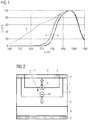
- the FIG. 1 shows in a diagram three transmission spectra a to c, in each of which the relative transmission (S rel ) in percent over a wavelength ( ⁇ ) of 400 nm to 1100 nm was plotted.
- the 100 percent represent the highest transmission achieved in this wavelength range, which was achieved for the respective curve.
- a calibrated monochromator from Bentem was used as the radiation source for the measurements.
- a chip with a known photosensitivity was cast in a housing.
- the potting material used was the material to be measured.
- the curve a shows the course of the relative transmission for the pure silicone to which no dye was added.
- the curve a rises steadily in the wavelength range from 400 nm to about 950 nm and approximately linear, ie with the same slope.
- the curve drops steeply parabolic in the further course, until it reaches a value for the relative transmission of almost 20% at a wavelength range of 1100 nm.
- the curve b shows the course of the relative transmission for a composition Z b .
- the composition Z b hereby comprises a two-component silicone system (Shin Etsu KJR 9022 E1) in an amount of 98.4% by mass, an orange dye in an amount of 0.08% by mass, a violet dye in an amount of 0.53% by mass first green dye at a mass fraction of 0.20 mass percent, and a second green dye at a fraction of 0.19 mass percent.
- the curve b increases steeply parabolic and reaches its maximum relative transmission at a wavelength of about 950 nm. After passing through the maximum The curve drops steeply like the curve a in a parabolic shape.
- the curve c shows the relative transmission of the composition Z c .
- the composition Z c comprises a two-component silicone system (Shin Etsu KJR 9022 E1) in an amount of 98.2 percent by mass, an orange dye in an amount of 0.17 mass percent, a violet dye in a proportion of 1.06 mass percent, a first green dye at a level of 0.40 mass% and a second green colorant at 0.37 mass%.
- the curve c likewise has virtually no relative transmission from the wavelength range from 400 nm to 700 nm. In the wavelength range of 750 to 900 nm, the curve c has a similar steep rise as the curve b, however, the curve of the curve c is slightly shifted to higher wavelengths. The curve c also reaches its maximum relative transmission at a wavelength of 950 nm and drops steeply parabolically after this as well as the other two curves.
- FIG. 1 It can be seen that by the addition of a suitable combination of dyes in the wavelength range of 400 to 700 nm, a very good filter function can be achieved, which is not the case with a pure silicone, as shown in curve a.
- Both the composition Z b and the composition Z c have a steep absorption edge, which can be seen in the steep rise of the two curves in the range from about 750 nm to 900 nm.
- the compositions Z b and Z c are very suitable as, for example, daylight filters. You can, for example be used for optoelectronic components, which work with electromagnetic radiation from the wavelength range of, for example, 900 to 1000 nm.
- FIG. 2 shows a schematic side view of an embodiment of an optoelectronic component, which is formed as a photodiode.
- This photodiode comprises a daylight filter 1, which is made of a material as described in the application.
- the daylight filter 1 and the first electrical contact 2 are arranged on a heavily p-doped zone 7.
- the heavily p-doped zone 7 is surrounded at its side surfaces, as well as from the bottom of a p-doped zone 6.
- this is followed by an n-doped zone 5 toward the side surfaces as well as toward the underside.
- the n-doped zone 5 is placed on a heavily n-doped zone 4, which in turn is arranged on a second electrical contact 3.
- the edge regions of the upper side are provided with a dielectric 8.
- the electromagnetic radiation here shown for example as photon 9
- the energy of the photon 9 for charge separation can lead to an electron 10 and a hole 11.
- the electron 10 or hole 11 can then migrate to the second electronic contact or first electronic contact of the component.
- the migration of the charge carriers leads to a current flow in the component.
- the daylight filter 1 can now prevent the incidence of electromagnetic radiation from the wavelength range of daylight photons in the interior of the Arrive photodiode and there trigger an unwanted current flow and thus a non-desired background signal in the photodiode by charge separation.
Landscapes
- Physics & Mathematics (AREA)
- Chemical & Material Sciences (AREA)
- General Physics & Mathematics (AREA)
- Optics & Photonics (AREA)
- Organic Chemistry (AREA)
- Health & Medical Sciences (AREA)
- Chemical Kinetics & Catalysis (AREA)
- Life Sciences & Earth Sciences (AREA)
- Toxicology (AREA)
- Engineering & Computer Science (AREA)
- Materials Engineering (AREA)
- Wood Science & Technology (AREA)
- Polymers & Plastics (AREA)
- Medicinal Chemistry (AREA)
- Spectroscopy & Molecular Physics (AREA)
- Optical Filters (AREA)
- Compositions Of Macromolecular Compounds (AREA)
- Solid State Image Pick-Up Elements (AREA)
Applications Claiming Priority (2)
| Application Number | Priority Date | Filing Date | Title |
|---|---|---|---|
| DE102009031915A DE102009031915A1 (de) | 2009-07-06 | 2009-07-06 | Zusammensetzung zur Herstellung eines Filtermaterials für Strahlung, Verfahren zur Herstellung einer Zusammensetzung für ein Filtermaterial, Material zur Filterung von Strahlung und ein optoelektronisches Bauelement umfassend das Material |
| PCT/EP2010/059288 WO2011003788A1 (de) | 2009-07-06 | 2010-06-30 | Zusammensetzung zur herstellung eines filtermaterials für strahlung, verfahren zur herstellung einer zusammensetzung für ein filtermaterial, material zur filterung von strahlung und ein optoelektronisches bauelement umfassend das material |
Publications (2)
| Publication Number | Publication Date |
|---|---|
| EP2452215A1 EP2452215A1 (de) | 2012-05-16 |
| EP2452215B1 true EP2452215B1 (de) | 2017-08-09 |
Family
ID=42350117
Family Applications (1)
| Application Number | Title | Priority Date | Filing Date |
|---|---|---|---|
| EP10726980.5A Active EP2452215B1 (de) | 2009-07-06 | 2010-06-30 | Zusammensetzung zur herstellung eines filtermaterials für strahlung, verfahren zur herstellung einer zusammensetzung für ein filtermaterial, material zur filterung von strahlung und ein optoelektronisches bauelement umfassend das material |
Country Status (7)
| Country | Link |
|---|---|
| US (1) | US9310538B2 (enExample) |
| EP (1) | EP2452215B1 (enExample) |
| JP (2) | JP2012532353A (enExample) |
| KR (1) | KR101700469B1 (enExample) |
| CN (1) | CN102483478B (enExample) |
| DE (1) | DE102009031915A1 (enExample) |
| WO (1) | WO2011003788A1 (enExample) |
Families Citing this family (5)
| Publication number | Priority date | Publication date | Assignee | Title |
|---|---|---|---|---|
| CN103665778B (zh) | 2012-08-30 | 2016-05-04 | 普立万聚合体(上海)有限公司 | 保护β-胡萝卜素的组合物 |
| CN103275515B (zh) * | 2013-06-18 | 2014-10-29 | 海宁市现代化工有限公司 | 一种橙色萘环酮染料及其制备方法 |
| DE102014206995A1 (de) * | 2014-04-11 | 2015-10-15 | Osram Opto Semiconductors Gmbh | Optoelektronisches Halbleiterelement, optoelektronisches Halbleiterbauteil und Verfahren zur Herstellung einer Mehrzahl von optoelektronischen Halbleiterelementen |
| US10363710B2 (en) * | 2016-01-22 | 2019-07-30 | Indizen Optical Technologies of America, LLC | Creating homogeneous optical elements by additive manufacturing |
| DE102023134624A1 (de) * | 2023-12-11 | 2025-06-12 | Ams-Osram International Gmbh | Filterelement, optoelektronisches bauelement, verfahren zur herstellung eines filterelements und verfahren zur herstellung eines optoelektronischen bauelements |
Citations (1)
| Publication number | Priority date | Publication date | Assignee | Title |
|---|---|---|---|---|
| WO2008035554A1 (en) * | 2006-09-20 | 2008-03-27 | Konica Minolta Holdings, Inc. | Novel squarylium metal complex compound, dye, and composition, color toner, ink, optical recording medium, color filter and front filter for display containing the same |
Family Cites Families (14)
| Publication number | Priority date | Publication date | Assignee | Title |
|---|---|---|---|---|
| US3620888A (en) | 1966-09-02 | 1971-11-16 | Polaroid Corp | Transparent laminate having at least one layer of a cellulose derivative matrix containing infrared absorber |
| GB1201066A (en) * | 1966-09-02 | 1970-08-05 | Polaroid Corp | Plastics optical elements |
| US4039467A (en) * | 1975-06-16 | 1977-08-02 | American Cyanamid Company | Visibly opaque infrared transmitting optical filter containing a combination of copper and vanadyl phthalocyanine sulfonamides |
| US5596025A (en) * | 1994-06-30 | 1997-01-21 | Minnesota Mining And Manufacturing Company | Dental impression material with cure-indicating dye |
| JPH09132718A (ja) | 1995-11-08 | 1997-05-20 | Toray Dow Corning Silicone Co Ltd | 二液型硬化性液状シリコーン組成物 |
| US6399190B1 (en) | 1996-07-25 | 2002-06-04 | Raytheon Company | Infrared-transparent structure including an adherent, infrared-transparent polymer layer |
| JP4105440B2 (ja) | 2002-01-30 | 2008-06-25 | 浜松ホトニクス株式会社 | 半導体光検出装置 |
| JP2003262701A (ja) | 2002-03-08 | 2003-09-19 | Kanegafuchi Chem Ind Co Ltd | 光学材料用組成物、光学材料、それを用いた液晶表示装置、発光ダイオードおよびそれらの製造方法 |
| JP4426793B2 (ja) | 2003-08-21 | 2010-03-03 | 株式会社朝日ラバー | 樹脂複合体及びその製造方法 |
| CN101472738B (zh) * | 2006-06-16 | 2013-11-06 | 阿基里斯株式会社 | 在近红外线区域具有光反射性能的深色片状物 |
| US7727418B2 (en) * | 2006-06-19 | 2010-06-01 | Sabic Innovative Plastics Ip B.V. | Infrared transmissive thermoplastic composition, and articles formed therefrom |
| JP4653028B2 (ja) | 2006-06-30 | 2011-03-16 | 三菱エンジニアリングプラスチックス株式会社 | ポリカーボネート樹脂組成物及び赤外線レーザー用フィルター |
| US20080103267A1 (en) * | 2006-10-31 | 2008-05-01 | General Electric Company | Infrared transmissive thermoplastic composition |
| US20080285165A1 (en) * | 2007-05-14 | 2008-11-20 | Wu Kuohua Angus | Thin film filter system and method |
-
2009
- 2009-07-06 DE DE102009031915A patent/DE102009031915A1/de not_active Withdrawn
-
2010
- 2010-06-30 CN CN201080030806.5A patent/CN102483478B/zh active Active
- 2010-06-30 US US13/379,257 patent/US9310538B2/en active Active
- 2010-06-30 EP EP10726980.5A patent/EP2452215B1/de active Active
- 2010-06-30 WO PCT/EP2010/059288 patent/WO2011003788A1/de not_active Ceased
- 2010-06-30 JP JP2012518898A patent/JP2012532353A/ja active Pending
- 2010-06-30 KR KR1020127001086A patent/KR101700469B1/ko active Active
-
2014
- 2014-10-07 JP JP2014206491A patent/JP5933663B2/ja not_active Expired - Fee Related
Patent Citations (1)
| Publication number | Priority date | Publication date | Assignee | Title |
|---|---|---|---|---|
| WO2008035554A1 (en) * | 2006-09-20 | 2008-03-27 | Konica Minolta Holdings, Inc. | Novel squarylium metal complex compound, dye, and composition, color toner, ink, optical recording medium, color filter and front filter for display containing the same |
Also Published As
| Publication number | Publication date |
|---|---|
| JP2012532353A (ja) | 2012-12-13 |
| US20120104291A1 (en) | 2012-05-03 |
| KR101700469B1 (ko) | 2017-01-26 |
| JP5933663B2 (ja) | 2016-06-15 |
| EP2452215A1 (de) | 2012-05-16 |
| DE102009031915A1 (de) | 2011-01-13 |
| JP2015072476A (ja) | 2015-04-16 |
| WO2011003788A1 (de) | 2011-01-13 |
| CN102483478A (zh) | 2012-05-30 |
| CN102483478B (zh) | 2014-09-24 |
| KR20120107913A (ko) | 2012-10-04 |
| US9310538B2 (en) | 2016-04-12 |
Similar Documents
| Publication | Publication Date | Title |
|---|---|---|
| DE69425998T2 (de) | Polymerdispergierte Flüssigkristallanzeige-Vorrichtung und Verfahren zu ihrer Herstellung | |
| DE69610193T2 (de) | Verfahren zur herstellung eines schaltbaren cholesterischen filters, sowie auch einer beleuchtungsanlage mit solchen filtern | |
| DE69215769T2 (de) | Flüssigkristallanzeigeelement | |
| EP2452215B1 (de) | Zusammensetzung zur herstellung eines filtermaterials für strahlung, verfahren zur herstellung einer zusammensetzung für ein filtermaterial, material zur filterung von strahlung und ein optoelektronisches bauelement umfassend das material | |
| DE69031240T2 (de) | Durchsichtige, optisch veränderliche Anordnung | |
| DE60108913T2 (de) | Dispergierte Nanoteilchen-enthaltende Struktur und diese Strukturen enthaltende Laminate | |
| DE19826008B4 (de) | Mehrbereichs-Flüssigkristallanzeigepaneel und Herstellungsverfahren für ein Mehrbereichs-Flüssigkristallanzeigepaneel | |
| DE69734431T2 (de) | Transparante leitfolie, schwach reflektierende transparante leitfolie, und anzeige | |
| DE69824062T2 (de) | Flüssigkristallanzeigevorrichtung und Herstellungsverfahren der Flüssigkristallanzeigevorrichtung | |
| US10308823B2 (en) | Near-infrared absorbing fine particle dispersion liquid and method for producing the same | |
| DE69518313T2 (de) | Flüssigkristallcomposit und verfahren zu dessen herstellung | |
| EP3252116B1 (en) | Near-infrared ray absorbing microparticle dispersion solution and production method thereof | |
| DE69524287T2 (de) | Polymerzusammensetzungen mit geringer Ausdehnung | |
| DE112004000337T5 (de) | Eingekapselte Nanopartikel zur Absorption von elektromagnetischer Energie | |
| DE69837961T2 (de) | Bestrahlungsvorrichtung für eine Orientierungsschicht für Flüssigkristallanzeigen | |
| DE69815560T2 (de) | Reflektive Flüssigkristallanzeigevorrichtung und Verfahren zu ihrer Herstellung | |
| DE102008060281B4 (de) | Reflektierender Flächenlichtmodulator | |
| DE69518658T2 (de) | Verfahren zur tränkung einer komponente in einem flüssigkristall-kompositmaterial und vorrichtungen, die dieses material verwenden | |
| DE4430859C2 (de) | Antireflexionsfilm | |
| DE112010003375T5 (de) | Acrylharzzusammensetzung, Verfahren zu deren Herstellung und Baumaterial, Modeaccessoire und optisches Material, gebildet unter deren Verwendung | |
| DE112018001039T5 (de) | Verfahren zur Herstellung eines Schichtkörpers und lichthärtbare Harzzusammensetzung | |
| WO2014019988A1 (de) | Optoelektronisches halbleiterbauelement und verfahren zur seiner herstellung | |
| DE102016105039B4 (de) | Touchfähiges Glas- oder Glaskeramikelement mit verminderter Lichtstreuung und/oder Lichtablenkung sowie Verfahren zu dessen Herstellung | |
| DE112020006175T5 (de) | Halbleiter-Nanoteilchenaggregat, Halbleiter-Nanoteilchenaggregat-Dispersionsflüssigkeit, Halbleiter-Nanoteilchenaggregat-Zusammensetzung und ausgehärteten Halbleiter-Nanoteilchenaggregat-Film | |
| DE102007058649A1 (de) | Auslesen von Informationen auf Halbleiter-Substraten |
Legal Events
| Date | Code | Title | Description |
|---|---|---|---|
| PUAI | Public reference made under article 153(3) epc to a published international application that has entered the european phase |
Free format text: ORIGINAL CODE: 0009012 |
|
| 17P | Request for examination filed |
Effective date: 20120102 |
|
| AK | Designated contracting states |
Kind code of ref document: A1 Designated state(s): AL AT BE BG CH CY CZ DE DK EE ES FI FR GB GR HR HU IE IS IT LI LT LU LV MC MK MT NL NO PL PT RO SE SI SK SM TR |
|
| DAX | Request for extension of the european patent (deleted) | ||
| 17Q | First examination report despatched |
Effective date: 20140311 |
|
| REG | Reference to a national code |
Ref country code: DE Ref legal event code: R079 Ref document number: 502010013981 Country of ref document: DE Free format text: PREVIOUS MAIN CLASS: G02B0005200000 Ipc: C09D0183040000 |
|
| GRAP | Despatch of communication of intention to grant a patent |
Free format text: ORIGINAL CODE: EPIDOSNIGR1 |
|
| RIC1 | Information provided on ipc code assigned before grant |
Ipc: H01L 31/0232 20140101ALI20170112BHEP Ipc: C08K 13/02 20060101ALI20170112BHEP Ipc: G02B 5/20 20060101ALI20170112BHEP Ipc: G02B 5/22 20060101ALI20170112BHEP Ipc: C08L 83/04 20060101ALI20170112BHEP Ipc: C09D 183/04 20060101AFI20170112BHEP |
|
| INTG | Intention to grant announced |
Effective date: 20170201 |
|
| GRAS | Grant fee paid |
Free format text: ORIGINAL CODE: EPIDOSNIGR3 |
|
| GRAA | (expected) grant |
Free format text: ORIGINAL CODE: 0009210 |
|
| AK | Designated contracting states |
Kind code of ref document: B1 Designated state(s): AL AT BE BG CH CY CZ DE DK EE ES FI FR GB GR HR HU IE IS IT LI LT LU LV MC MK MT NL NO PL PT RO SE SI SK SM TR |
|
| REG | Reference to a national code |
Ref country code: GB Ref legal event code: FG4D Free format text: NOT ENGLISH |
|
| REG | Reference to a national code |
Ref country code: CH Ref legal event code: EP Ref country code: AT Ref legal event code: REF Ref document number: 916808 Country of ref document: AT Kind code of ref document: T Effective date: 20170815 |
|
| REG | Reference to a national code |
Ref country code: IE Ref legal event code: FG4D Free format text: LANGUAGE OF EP DOCUMENT: GERMAN |
|
| REG | Reference to a national code |
Ref country code: DE Ref legal event code: R096 Ref document number: 502010013981 Country of ref document: DE |
|
| REG | Reference to a national code |
Ref country code: NL Ref legal event code: MP Effective date: 20170809 |
|
| REG | Reference to a national code |
Ref country code: LT Ref legal event code: MG4D |
|
| PG25 | Lapsed in a contracting state [announced via postgrant information from national office to epo] |
Ref country code: LT Free format text: LAPSE BECAUSE OF FAILURE TO SUBMIT A TRANSLATION OF THE DESCRIPTION OR TO PAY THE FEE WITHIN THE PRESCRIBED TIME-LIMIT Effective date: 20170809 Ref country code: NL Free format text: LAPSE BECAUSE OF FAILURE TO SUBMIT A TRANSLATION OF THE DESCRIPTION OR TO PAY THE FEE WITHIN THE PRESCRIBED TIME-LIMIT Effective date: 20170809 Ref country code: FI Free format text: LAPSE BECAUSE OF FAILURE TO SUBMIT A TRANSLATION OF THE DESCRIPTION OR TO PAY THE FEE WITHIN THE PRESCRIBED TIME-LIMIT Effective date: 20170809 Ref country code: HR Free format text: LAPSE BECAUSE OF FAILURE TO SUBMIT A TRANSLATION OF THE DESCRIPTION OR TO PAY THE FEE WITHIN THE PRESCRIBED TIME-LIMIT Effective date: 20170809 Ref country code: SE Free format text: LAPSE BECAUSE OF FAILURE TO SUBMIT A TRANSLATION OF THE DESCRIPTION OR TO PAY THE FEE WITHIN THE PRESCRIBED TIME-LIMIT Effective date: 20170809 Ref country code: NO Free format text: LAPSE BECAUSE OF FAILURE TO SUBMIT A TRANSLATION OF THE DESCRIPTION OR TO PAY THE FEE WITHIN THE PRESCRIBED TIME-LIMIT Effective date: 20171109 |
|
| PG25 | Lapsed in a contracting state [announced via postgrant information from national office to epo] |
Ref country code: BG Free format text: LAPSE BECAUSE OF FAILURE TO SUBMIT A TRANSLATION OF THE DESCRIPTION OR TO PAY THE FEE WITHIN THE PRESCRIBED TIME-LIMIT Effective date: 20171109 Ref country code: GR Free format text: LAPSE BECAUSE OF FAILURE TO SUBMIT A TRANSLATION OF THE DESCRIPTION OR TO PAY THE FEE WITHIN THE PRESCRIBED TIME-LIMIT Effective date: 20171110 Ref country code: PL Free format text: LAPSE BECAUSE OF FAILURE TO SUBMIT A TRANSLATION OF THE DESCRIPTION OR TO PAY THE FEE WITHIN THE PRESCRIBED TIME-LIMIT Effective date: 20170809 Ref country code: IS Free format text: LAPSE BECAUSE OF FAILURE TO SUBMIT A TRANSLATION OF THE DESCRIPTION OR TO PAY THE FEE WITHIN THE PRESCRIBED TIME-LIMIT Effective date: 20171209 Ref country code: LV Free format text: LAPSE BECAUSE OF FAILURE TO SUBMIT A TRANSLATION OF THE DESCRIPTION OR TO PAY THE FEE WITHIN THE PRESCRIBED TIME-LIMIT Effective date: 20170809 Ref country code: ES Free format text: LAPSE BECAUSE OF FAILURE TO SUBMIT A TRANSLATION OF THE DESCRIPTION OR TO PAY THE FEE WITHIN THE PRESCRIBED TIME-LIMIT Effective date: 20170809 |
|
| PG25 | Lapsed in a contracting state [announced via postgrant information from national office to epo] |
Ref country code: DK Free format text: LAPSE BECAUSE OF FAILURE TO SUBMIT A TRANSLATION OF THE DESCRIPTION OR TO PAY THE FEE WITHIN THE PRESCRIBED TIME-LIMIT Effective date: 20170809 Ref country code: RO Free format text: LAPSE BECAUSE OF FAILURE TO SUBMIT A TRANSLATION OF THE DESCRIPTION OR TO PAY THE FEE WITHIN THE PRESCRIBED TIME-LIMIT Effective date: 20170809 Ref country code: CZ Free format text: LAPSE BECAUSE OF FAILURE TO SUBMIT A TRANSLATION OF THE DESCRIPTION OR TO PAY THE FEE WITHIN THE PRESCRIBED TIME-LIMIT Effective date: 20170809 |
|
| REG | Reference to a national code |
Ref country code: DE Ref legal event code: R097 Ref document number: 502010013981 Country of ref document: DE |
|
| PG25 | Lapsed in a contracting state [announced via postgrant information from national office to epo] |
Ref country code: IT Free format text: LAPSE BECAUSE OF FAILURE TO SUBMIT A TRANSLATION OF THE DESCRIPTION OR TO PAY THE FEE WITHIN THE PRESCRIBED TIME-LIMIT Effective date: 20170809 Ref country code: SM Free format text: LAPSE BECAUSE OF FAILURE TO SUBMIT A TRANSLATION OF THE DESCRIPTION OR TO PAY THE FEE WITHIN THE PRESCRIBED TIME-LIMIT Effective date: 20170809 Ref country code: EE Free format text: LAPSE BECAUSE OF FAILURE TO SUBMIT A TRANSLATION OF THE DESCRIPTION OR TO PAY THE FEE WITHIN THE PRESCRIBED TIME-LIMIT Effective date: 20170809 Ref country code: SK Free format text: LAPSE BECAUSE OF FAILURE TO SUBMIT A TRANSLATION OF THE DESCRIPTION OR TO PAY THE FEE WITHIN THE PRESCRIBED TIME-LIMIT Effective date: 20170809 |
|
| PLBE | No opposition filed within time limit |
Free format text: ORIGINAL CODE: 0009261 |
|
| STAA | Information on the status of an ep patent application or granted ep patent |
Free format text: STATUS: NO OPPOSITION FILED WITHIN TIME LIMIT |
|
| 26N | No opposition filed |
Effective date: 20180511 |
|
| PG25 | Lapsed in a contracting state [announced via postgrant information from national office to epo] |
Ref country code: SI Free format text: LAPSE BECAUSE OF FAILURE TO SUBMIT A TRANSLATION OF THE DESCRIPTION OR TO PAY THE FEE WITHIN THE PRESCRIBED TIME-LIMIT Effective date: 20170809 |
|
| PG25 | Lapsed in a contracting state [announced via postgrant information from national office to epo] |
Ref country code: MT Free format text: LAPSE BECAUSE OF FAILURE TO SUBMIT A TRANSLATION OF THE DESCRIPTION OR TO PAY THE FEE WITHIN THE PRESCRIBED TIME-LIMIT Effective date: 20170809 |
|
| REG | Reference to a national code |
Ref country code: CH Ref legal event code: PL |
|
| GBPC | Gb: european patent ceased through non-payment of renewal fee |
Effective date: 20180630 |
|
| REG | Reference to a national code |
Ref country code: BE Ref legal event code: MM Effective date: 20180630 |
|
| PG25 | Lapsed in a contracting state [announced via postgrant information from national office to epo] |
Ref country code: LU Free format text: LAPSE BECAUSE OF NON-PAYMENT OF DUE FEES Effective date: 20180630 Ref country code: MC Free format text: LAPSE BECAUSE OF FAILURE TO SUBMIT A TRANSLATION OF THE DESCRIPTION OR TO PAY THE FEE WITHIN THE PRESCRIBED TIME-LIMIT Effective date: 20170809 |
|
| REG | Reference to a national code |
Ref country code: IE Ref legal event code: MM4A |
|
| PG25 | Lapsed in a contracting state [announced via postgrant information from national office to epo] |
Ref country code: CH Free format text: LAPSE BECAUSE OF NON-PAYMENT OF DUE FEES Effective date: 20180630 Ref country code: LI Free format text: LAPSE BECAUSE OF NON-PAYMENT OF DUE FEES Effective date: 20180630 Ref country code: FR Free format text: LAPSE BECAUSE OF NON-PAYMENT OF DUE FEES Effective date: 20180630 Ref country code: IE Free format text: LAPSE BECAUSE OF NON-PAYMENT OF DUE FEES Effective date: 20180630 Ref country code: GB Free format text: LAPSE BECAUSE OF NON-PAYMENT OF DUE FEES Effective date: 20180630 |
|
| PG25 | Lapsed in a contracting state [announced via postgrant information from national office to epo] |
Ref country code: BE Free format text: LAPSE BECAUSE OF NON-PAYMENT OF DUE FEES Effective date: 20180630 |
|
| REG | Reference to a national code |
Ref country code: AT Ref legal event code: MM01 Ref document number: 916808 Country of ref document: AT Kind code of ref document: T Effective date: 20180630 |
|
| PG25 | Lapsed in a contracting state [announced via postgrant information from national office to epo] |
Ref country code: AT Free format text: LAPSE BECAUSE OF NON-PAYMENT OF DUE FEES Effective date: 20180630 |
|
| PG25 | Lapsed in a contracting state [announced via postgrant information from national office to epo] |
Ref country code: TR Free format text: LAPSE BECAUSE OF FAILURE TO SUBMIT A TRANSLATION OF THE DESCRIPTION OR TO PAY THE FEE WITHIN THE PRESCRIBED TIME-LIMIT Effective date: 20170809 |
|
| PG25 | Lapsed in a contracting state [announced via postgrant information from national office to epo] |
Ref country code: PT Free format text: LAPSE BECAUSE OF FAILURE TO SUBMIT A TRANSLATION OF THE DESCRIPTION OR TO PAY THE FEE WITHIN THE PRESCRIBED TIME-LIMIT Effective date: 20170809 Ref country code: HU Free format text: LAPSE BECAUSE OF FAILURE TO SUBMIT A TRANSLATION OF THE DESCRIPTION OR TO PAY THE FEE WITHIN THE PRESCRIBED TIME-LIMIT; INVALID AB INITIO Effective date: 20100630 |
|
| PG25 | Lapsed in a contracting state [announced via postgrant information from national office to epo] |
Ref country code: CY Free format text: LAPSE BECAUSE OF FAILURE TO SUBMIT A TRANSLATION OF THE DESCRIPTION OR TO PAY THE FEE WITHIN THE PRESCRIBED TIME-LIMIT Effective date: 20170809 Ref country code: MK Free format text: LAPSE BECAUSE OF NON-PAYMENT OF DUE FEES Effective date: 20170809 |
|
| PG25 | Lapsed in a contracting state [announced via postgrant information from national office to epo] |
Ref country code: AL Free format text: LAPSE BECAUSE OF FAILURE TO SUBMIT A TRANSLATION OF THE DESCRIPTION OR TO PAY THE FEE WITHIN THE PRESCRIBED TIME-LIMIT Effective date: 20170809 |
|
| P01 | Opt-out of the competence of the unified patent court (upc) registered |
Effective date: 20230825 |
|
| PGFP | Annual fee paid to national office [announced via postgrant information from national office to epo] |
Ref country code: DE Payment date: 20250618 Year of fee payment: 16 |