EP2446067B1 - Verfahren zur nassätzung eines selbstanordnenden einschichtigen strukturierten substrats und metallstrukturierte artikel - Google Patents
Verfahren zur nassätzung eines selbstanordnenden einschichtigen strukturierten substrats und metallstrukturierte artikel Download PDFInfo
- Publication number
- EP2446067B1 EP2446067B1 EP10728512.4A EP10728512A EP2446067B1 EP 2446067 B1 EP2446067 B1 EP 2446067B1 EP 10728512 A EP10728512 A EP 10728512A EP 2446067 B1 EP2446067 B1 EP 2446067B1
- Authority
- EP
- European Patent Office
- Prior art keywords
- metal
- pattern
- substrate
- patterned
- region
- Prior art date
- Legal status (The legal status is an assumption and is not a legal conclusion. Google has not performed a legal analysis and makes no representation as to the accuracy of the status listed.)
- Active
Links
Images
Classifications
-
- C—CHEMISTRY; METALLURGY
- C23—COATING METALLIC MATERIAL; COATING MATERIAL WITH METALLIC MATERIAL; CHEMICAL SURFACE TREATMENT; DIFFUSION TREATMENT OF METALLIC MATERIAL; COATING BY VACUUM EVAPORATION, BY SPUTTERING, BY ION IMPLANTATION OR BY CHEMICAL VAPOUR DEPOSITION, IN GENERAL; INHIBITING CORROSION OF METALLIC MATERIAL OR INCRUSTATION IN GENERAL
- C23F—NON-MECHANICAL REMOVAL OF METALLIC MATERIAL FROM SURFACE; INHIBITING CORROSION OF METALLIC MATERIAL OR INCRUSTATION IN GENERAL; MULTI-STEP PROCESSES FOR SURFACE TREATMENT OF METALLIC MATERIAL INVOLVING AT LEAST ONE PROCESS PROVIDED FOR IN CLASS C23 AND AT LEAST ONE PROCESS COVERED BY SUBCLASS C21D OR C22F OR CLASS C25
- C23F1/00—Etching metallic material by chemical means
- C23F1/02—Local etching
-
- C—CHEMISTRY; METALLURGY
- C23—COATING METALLIC MATERIAL; COATING MATERIAL WITH METALLIC MATERIAL; CHEMICAL SURFACE TREATMENT; DIFFUSION TREATMENT OF METALLIC MATERIAL; COATING BY VACUUM EVAPORATION, BY SPUTTERING, BY ION IMPLANTATION OR BY CHEMICAL VAPOUR DEPOSITION, IN GENERAL; INHIBITING CORROSION OF METALLIC MATERIAL OR INCRUSTATION IN GENERAL
- C23F—NON-MECHANICAL REMOVAL OF METALLIC MATERIAL FROM SURFACE; INHIBITING CORROSION OF METALLIC MATERIAL OR INCRUSTATION IN GENERAL; MULTI-STEP PROCESSES FOR SURFACE TREATMENT OF METALLIC MATERIAL INVOLVING AT LEAST ONE PROCESS PROVIDED FOR IN CLASS C23 AND AT LEAST ONE PROCESS COVERED BY SUBCLASS C21D OR C22F OR CLASS C25
- C23F1/00—Etching metallic material by chemical means
- C23F1/08—Apparatus, e.g. for photomechanical printing surfaces
-
- H—ELECTRICITY
- H05—ELECTRIC TECHNIQUES NOT OTHERWISE PROVIDED FOR
- H05K—PRINTED CIRCUITS; CASINGS OR CONSTRUCTIONAL DETAILS OF ELECTRIC APPARATUS; MANUFACTURE OF ASSEMBLAGES OF ELECTRICAL COMPONENTS
- H05K3/00—Apparatus or processes for manufacturing printed circuits
- H05K3/02—Apparatus or processes for manufacturing printed circuits in which the conductive material is applied to the surface of the insulating support and is thereafter removed from such areas of the surface which are not intended for current conducting or shielding
- H05K3/06—Apparatus or processes for manufacturing printed circuits in which the conductive material is applied to the surface of the insulating support and is thereafter removed from such areas of the surface which are not intended for current conducting or shielding the conductive material being removed chemically or electrolytically, e.g. by photo-etch process
- H05K3/061—Etching masks
-
- G—PHYSICS
- G03—PHOTOGRAPHY; CINEMATOGRAPHY; ANALOGOUS TECHNIQUES USING WAVES OTHER THAN OPTICAL WAVES; ELECTROGRAPHY; HOLOGRAPHY
- G03F—PHOTOMECHANICAL PRODUCTION OF TEXTURED OR PATTERNED SURFACES, e.g. FOR PRINTING, FOR PROCESSING OF SEMICONDUCTOR DEVICES; MATERIALS THEREFOR; ORIGINALS THEREFOR; APPARATUS SPECIALLY ADAPTED THEREFOR
- G03F7/00—Photomechanical, e.g. photolithographic, production of textured or patterned surfaces, e.g. printing surfaces; Materials therefor, e.g. comprising photoresists; Apparatus specially adapted therefor
- G03F7/26—Processing photosensitive materials; Apparatus therefor
- G03F7/40—Treatment after imagewise removal, e.g. baking
-
- H—ELECTRICITY
- H05—ELECTRIC TECHNIQUES NOT OTHERWISE PROVIDED FOR
- H05K—PRINTED CIRCUITS; CASINGS OR CONSTRUCTIONAL DETAILS OF ELECTRIC APPARATUS; MANUFACTURE OF ASSEMBLAGES OF ELECTRICAL COMPONENTS
- H05K2203/00—Indexing scheme relating to apparatus or processes for manufacturing printed circuits covered by H05K3/00
- H05K2203/08—Treatments involving gases
- H05K2203/086—Using an inert gas
-
- H—ELECTRICITY
- H05—ELECTRIC TECHNIQUES NOT OTHERWISE PROVIDED FOR
- H05K—PRINTED CIRCUITS; CASINGS OR CONSTRUCTIONAL DETAILS OF ELECTRIC APPARATUS; MANUFACTURE OF ASSEMBLAGES OF ELECTRICAL COMPONENTS
- H05K2203/00—Indexing scheme relating to apparatus or processes for manufacturing printed circuits covered by H05K3/00
- H05K2203/12—Using specific substances
- H05K2203/122—Organic non-polymeric compounds, e.g. oil, wax, thiol
-
- H—ELECTRICITY
- H05—ELECTRIC TECHNIQUES NOT OTHERWISE PROVIDED FOR
- H05K—PRINTED CIRCUITS; CASINGS OR CONSTRUCTIONAL DETAILS OF ELECTRIC APPARATUS; MANUFACTURE OF ASSEMBLAGES OF ELECTRICAL COMPONENTS
- H05K3/00—Apparatus or processes for manufacturing printed circuits
- H05K3/02—Apparatus or processes for manufacturing printed circuits in which the conductive material is applied to the surface of the insulating support and is thereafter removed from such areas of the surface which are not intended for current conducting or shielding
- H05K3/06—Apparatus or processes for manufacturing printed circuits in which the conductive material is applied to the surface of the insulating support and is thereafter removed from such areas of the surface which are not intended for current conducting or shielding the conductive material being removed chemically or electrolytically, e.g. by photo-etch process
- H05K3/068—Apparatus for etching printed circuits
-
- Y—GENERAL TAGGING OF NEW TECHNOLOGICAL DEVELOPMENTS; GENERAL TAGGING OF CROSS-SECTIONAL TECHNOLOGIES SPANNING OVER SEVERAL SECTIONS OF THE IPC; TECHNICAL SUBJECTS COVERED BY FORMER USPC CROSS-REFERENCE ART COLLECTIONS [XRACs] AND DIGESTS
- Y10—TECHNICAL SUBJECTS COVERED BY FORMER USPC
- Y10T—TECHNICAL SUBJECTS COVERED BY FORMER US CLASSIFICATION
- Y10T428/00—Stock material or miscellaneous articles
- Y10T428/24—Structurally defined web or sheet [e.g., overall dimension, etc.]
- Y10T428/24802—Discontinuous or differential coating, impregnation or bond [e.g., artwork, printing, retouched photograph, etc.]
Definitions
- Microcontact printing uses micropatterned elastomeric stamps, typically made from polydimethyl siloxane (PDMS) that are inked and placed onto a substrate to localize a chemical reaction between molecules of the ink that are able to form a self-assembled monolayer (SAM) and the substrate.
- PDMS polydimethyl siloxane
- SAM self-assembled monolayer
- Kumar et al. "Patterning Self-Assembled Monolayers: Applications in Material Science", Langmuir, Amercian Chemical Society, vol. 10, no. 5, 1994-05-01, pages 1498-1511 discloses a technique based on stamping or contact printing to pattern the adsorption of alkanethiolates on surfaces of gold.
- US 3 565 707 A describes a process for dissolving certain metals which are not etched by persulfate solutions alone.
- the method comprises providing a substrate comprising a metalized surface having a self-assembled monolayer patterned region and unpatterned region; and wet etching the substrate at a rate of at least 300 nm/minute to remove metal from the unpatterned regions thereby forming a metal pattern, wherein the wet etching comprises immersing the metallized surface comprising the self-assembled monolayer patterned region in a liquid etchant agitated with bubbling gas.
- the self-assembled monolayer patterned region is typically microcontact printed onto the metalized surface.
- Bubbles are emitted from a bubble generating surface and they move through the liquid etchant in a direction substantially normal to the metalized surface.
- the bubbles impinge upon the metalized surface comprising the patterned self-assembled monolayer.
- the metalized surface comprising the self-assembled monolayer patterned region is positioned substantially parallel to a bubble generating surface that emits bubbles.
- the metalized surface is positioned at a distance of at least 30 millimeters from the bubble generating surface.
- the bubble generating surface typically has surface area of at least about one third of that of the self-assembled monolayer pattern.
- the bubbles emitted from the bubble generating surface have a velocity of at least 10 cm/min. Further, the bubbles have a diameter of at least 2 millimeters at the metalized surface.
- the metal patterned article comprises a substrate and an etched microcontact printed metal pattern disposed on the substrate wherein the pattern has a thickness of at least 100 nanometers and a pattern feature uniformity of at least 75%, or 90% throughout an area of at least 25 cm 2 .
- the pattern comprises silver or gold having a thickness of at least 250 nanometers.
- the present disclosure relates to a method of wet etching the metal of a substrate comprising a metalized surface having unpatterned regions and a patterned self-assembled monolayer (SAM).
- SAM self-assembled monolayer
- metal and metalized refers to an elemental metal or alloy that is suitably conductive for the intended purpose.
- the metalized substrate is typically a metal-coated visible light transparent substrate.
- visible light transparent refers to the level of transmission of unmetalized regions of the substrate being typically at least 80% transmissive to at least one polarization state of visible light, where the % transmission is normalized to the intensity of the incident, optionally polarized light.
- the regions of the substrate that comprise the (e.g. microcontact printed) metal pattern typically have a lower transmission.
- the average transmittance of the substrate with an etched microcontact printed metal pattern thereon, including both the patterned (i.e. metalized) and unpatterned (i.e,. unmetalized) regions is at least 60%.
- a polymeric "film” substrate is a polymer material in the form of a flat sheet that is sufficiently flexible and strong to be processed in a roll-to-roll fashion.
- roll-to-roll what is meant is a process where material is wound onto or unwound from a support, as well as further processed in some way. Examples of further processes include coating, slitting, blanking, and exposing to radiation, or the like.
- Polymeric films can be manufactured in a variety of thickness, ranging in general from about 5 ⁇ m to 1000 ⁇ m. In many embodiments, polymeric film thicknesses range from about 25 ⁇ m to about 500 ⁇ m, or from about 50 ⁇ m to about 250 ⁇ m, or from about 75 ⁇ m to about 200 ⁇ m.
- Roll-to-roll polymeric films may have a width of at least 30.5 cm (12 inches), 61 cm (24 inches), 91.5 cm (36 inches), or 122 cm (48 inches).
- thermoplastic and thermoset polymeric films include thermoplastic and thermoset polymeric films.
- thermoplastics include polyolefins, polyacrylates, polyamides, polyimides, polycarbonates, and polyesters.
- thermoplastics include polyethylene, polypropylene, poly(methylmethacrylate), polycarbonate of bisphenol A, poly(vinyl chloride), polyethylene terephthalate, and poly(vinylidene fluoride).
- the (e.g. polymeric film) substrate has a metallic coating disposed on at least one major surface.
- the surface of a substrate with a metallic coating disposed thereon is described herein as a metalized surface of a substrate.
- the metallic coating is typically a continuous metal coating that is then SAM patterned metal regions are retained on the substrate and the metal of the unpatterned regions is removed by wet etching, thereby forming a metal pattern.
- the metallic coating can be deposited using any convenient method, for example sputtering, evaporation, chemical vapor deposition, or chemical solution deposition (including electroless plating).
- the metallic coating comprises elemental metal, metal alloys, intermetallic compounds, metal oxides, metal sulfides, metal carbides, metal nitrides, or combinations thereof.
- Exemplary metals include gold, silver, palladium, platinum, rhodium, copper, nickel, iron, indium, tin, tantalum, as well as mixtures, alloys, and compounds of these elements.
- the metallic coatings can be various thicknesses. However, the thickness of the resulting conductive pattern is generally equal to the thickness of the metallic coating.
- the method of the present invention can also be used for relatively thin patterns, ranging in thickness from about 5 nanometers to about 50 nanometers, the method described herein is amenable to articles having increased metal pattern thicknesses, of at least 100 nm.
- the thickness of the (e.g. conductive) metal pattern is at least 250 nm.
- the silver micropatterns have thicknesses of at least 300 nm, 400 nm, 500 nm, 600 nm, 700 nm, 800 nm, 900 nm, and even 1000 nm or greater.
- the gold micropatterns have thicknesses of at least 300 nm, 350 nm, 400 nm, or greater.
- the metalized substrate surfaces can be treated by any of a number of different processes prior to application of the ink.
- optional treatment processes include ultraviolet light-ozone cleaning, oxygen plasma cleaning, solvent degreasing, high-pressure washing, and detergent-based cleaning.
- Patterning functionalizing molecules to generate a self-assembled monolayer pattern can be achieved using a number of different techniques, including microcontact printing, dip-pen nanolithography, photolithography, and ink-jet printing.
- a self-assembled monolayer patterned region is a portion of a metalized surface where a self-assembled monolayer exists (e.g. as applied by microcontact printing).
- an unpatterned region is a portion of a metalized surface where the self-assembled monolayer of the patterned region does not exist. It is within the scope of the invention for a different self-assembled monolayer to exist in the unpatterned region, provided that the presence thereof does not interfere with the etching.
- Microcontact printing typically utilizes a relief-patterned elastomeric stamp.
- Useful elastomers for forming the stamp include silicones, polyurethanes, ethylene propylene diene M-class (EPDM) rubbers, as well as the range of existing commercially available flexographic printing plate materials (for example, commercially available from E. I. du Pont de Nemours and Company, Wilmington, Delaware, under the trade name CyrelTM).
- the stamp can be made from a composite material (for example, one of the aforementioned elastomers combined with a woven or non-woven fibrous reinforcement).
- Polydimethylsiloxane is particularly useful as a stamp material, as it is elastomeric and has a low surface energy (which makes it easy to remove the stamp from most substrates).
- PDMS is also commercially available.
- a useful commercially available formulation is SylgardTM 184 PDMS (Dow Corning, Midland, Michigan).
- PDMS stamps can be formed, for example, by dispensing an uncrosslinked PDMS polymer into or against a patterned mold, followed by curing.
- the patterned features can be, for example, millimeter-sized, micrometer-sized, nanometer-sized, or a combination thereof.
- the master tool for molding the elastomeric stamps can be generated by preparing a patterned photoresist using photolithography as known in the art.
- the elastomeric stamp can be molded against the master tool by applying uncured PDMS to the master tool and then curing.
- Microcontact printing can be carried out by using a relief-patterned stamp or printing plate made of elastomer in combination with a substantially flat substrate in order to transfer to the substrate a patterned self-assembled monolayer (SAM) according to the relief pattern of the stamp or plate.
- microcontact printing can be carried out by using a substantially flat stamp or printing plate made of elastomer in combination with a relief-patterned (or structured or microstructured) substrate (for example, a coated polymer film with embossed surface structure on a major surface) in order to transfer to the substrate a patterned self-assembled monolayer (SAM) according to the relief pattern of the substrate (as described, for example, in U. S. Patent Application Publication No. 2008-0095985-A1 (Frey et al. ).
- the “ink” comprises molecules capable of forming a self-assembled monolayer.
- Various molecules that form a self-assembled monolayer (SAM) are known such as organosulfur compounds, organosilanes and organophosphonic acids.
- Organosulfur compounds include for example alkylthiols, dialkyl disulfides, dialkyl sulfides, alkyl xanthates, dithiophosphates, and dialkylthiocarbamates.
- the molecules are characterized by a tail group or groups attached to a sulfur atom, wherein the tail group or groups have between 14 and 20 atoms along their backbone, preferably 16, 17, or 18 atoms. The atoms along the backbone are preferably carbon atoms.
- Other useful chain lengths include 19 and 20.
- the chain length is determined as the number of atoms along the linear arrangement of bonded atoms between and including the atom that is bonded to the sulfur atom and final carbon atom in the linear arrangement.
- the monolayer-forming molecule may comprise other end groups or be branched (e.g. with side groups) provided that the molecule is suitable to form a self-assembled monolayer that functions as an etch resist.
- the SAM-forming molecules may also be partially fluorinated or perfluorinated, for example as described in US 2011/0226733 .
- such printing can include a displacement reaction that results in removal or modification of an atom or functional group in the SAM-forming molecules (for example, conversion of a thiol (R-SH compound) to a thiolate (R-S-M) monolayer when the monolayer is formed on a metal (M), for example silver or gold).
- R-SH compound thiol
- R-S-M thiolate
- M metal
- the resulting printed pattern can comprise compounds or molecules that are chemically different from the molecules of the ink composition.
- the ink compositions can further comprise at least one solvent.
- Suitable solvents for use in the ink compositions include alcohols, ketones, aromatic compounds, heterocyclic compounds, fluorinated solvents, and the like, and combinations thereof.
- Other useful solvents include dimethylformamide, acetonitrile, dimethylacetamide, dimethylsulfoxide, ethyl acetate, tetrahydrofuran (THF), methyl t-butyl ether (MTBE), and the like, and combinations thereof.
- the solvent of the ink composition can be selected so as to evaporate relatively rapidly from the stamp surface, as this can also be helpful for achieving a relatively uniform distribution of the SAM forming molecules on or within the stamp with a minimum of time and application of forced air.
- the solvents are chosen such that the solvent does not excessively swell the (e.g. PDMS) stamp.
- the ink compositions can comprise relatively small amounts of common additives (for example, stabilizers or desiccants), if desired, as known in the art.
- common additives for example, stabilizers or desiccants
- the stamp can be "inked” with a composition comprising molecules capable of forming a SAM using methods known in the art.
- an applicator for example, a cotton swab or a foam applicator
- the stamp can be rubbed across the relief-patterned surface of the stamp, followed by drying of solvent from the stamp surface.
- the stamp can be pressed against an "ink pad" impregnated with the ink composition, the ink pad optionally being a PDMS slab.
- the stamp can be charged with ink composition from its back side, relative to the printing surface. In this latter approach, the molecules diffuse through the stamp to reach the relief-patterned face for printing.
- the relief-patterned printing face of the stamp can be immersed in the ink, followed by withdrawal and drying ("immersive inking"). All of the above described methods of inking render the relief-patterned stamp surface inked, yielding an "inked surface.”
- the inked stamp can be used to transfer a pattern to the metalized surface of the substrate to form at least one SAM patterned region and (e.g. adjacent) unpatterned regions on the metalized surface.
- the inked surface of the stamp comprises a relief pattern
- the inked surface can be contacted to a surface of a substrate that is essentially flat in order to transfer a pattern of the SAM forming molecules to the metalized surface of the substrate, wherein the pattern of the SAM molecules is essentially the same as the pattern of raised features in the relief pattern of the inked surface of the stamp.
- the pattern is said to be transferred according to the relief pattern of the inked surface of the stamp.
- the inked surface of the stamp may be essentially flat, with the substrate comprising the relief pattern.
- Such "reverse" microcontact printing process is described for example in U.S. Patent No. 6,518,168 (Clem et al. ).
- the inked stamp can be placed in contact with the surface of the substrate such that contact is made with the raised regions of the relief-patterned surface of the stamp.
- the molecules can diffuse from the stamp onto the surface of the substrate where they can form a SAM.
- the printing time (that is, the duration of contact between the stamp and the substrate) can vary, depending upon factors including, for example, the concentration of the ink composition and the pressure applied to the stamp. In some embodiments, the print time can be less than 1 minute (preferably, less than about 30 seconds; more preferably, less than about 10 seconds; most preferably, less than about 5 seconds).
- the SAM patterned substrate can be used as a resist that protects the underlying substrate surface during a subsequent etching step. Thus, it can serve as an etch mask that protects against the action of an etchant, while the other region(s) (i.e. lacking the patterned monolayer) on the surface of the substrate are not protected, allowing selective removal of material (for example, metal) in the exposed region(s).
- Wet etching of the substrate is typically carried out by use of an etchant bath comprising an etchant solution.
- the etching of the exposed region is selective, i.e. without significant etching of the surface regions comprising the SAM pattern.
- less than about 50% by mass of the metal in the SAM patterned regions is removed via wet etching per unit area.
- less than about 25% by mass, less than about 10% by mass, or less than about 5% by mass of the metal in the SAM patterned regions are removed via wet etching per unit area. This can be determined by using known methods such as transmitted light attenuation, profilometry, mass analysis, or the like.
- Useful chemical etching baths can be prepared by dissolving etchant species in water or a non-aqueous solvent (for example, with agitation or stirring, control of pH, control of temperature, and/or replenishment of etchant species upon their consumption, according to the nature of the etchant).
- the etchant bath typically comprises at least one oxidizing agent.
- the oxidizing agent particularly for etching silver or gold, can be a relatively small molecule oxidizing agent, typically have a molecular weight of less than about 200 g/mole.
- Suitable small molecule oxidizing agents include for example cyanide ions in the presence of dissolved oxygen, ferricyanide ions, and ferric ions.
- Thiourea and thiourea derivatives are related to thioamides e.g. RC(S)NR 2 , where R is methyl, ethyl, etc.
- a small molecule metal complexing compound also having a molecular weight less than about 200 g/mole is employed.
- Thiourea-based etchants with ferric ions as an oxidizing species are generally preferred etchant solutions, particularly for etching silver or gold.
- the concentration of oxidizing species is typically at least 1 mM or 5 mM and no greater than 500 mM or 250 mM. In some embodiments, the concentration of oxidizing species (e.g. ferric nitrate) is at least 10 mM, 15 mM, or 20 mM and no greater than 100 mM or 50 mM.
- the etchant comprises oxidizing species in the absence of a metal complexing compound, such as thiourea.
- a metal complexing compound e.g. thiourea
- a metal complexing compound is present in the etchant bath at a concentration of at least 1 mM or 5 mM and no greater than 250 mM or 100 mM.
- the concentration of metal complexing compound is at least 10 mM or 15 mM and no greater than 100 mM.
- the etchant may also comprise self-assembling monolayer forming molecules.
- good pattern feature uniformity, increased metal pattern thickness, or a combination thereof were obtained using a liquid etchant that is free of self-assembling monolayer forming molecules.
- the etchant is generally added to the etchant bath and circulated.
- the concentration may be monitored and adjusted to maintain a constant concentration for the duration of the etching.
- the invention is not limited with regard to the physical mechanism (e.g. bubbler apparatus) that is used for agitating the etchant solution with bubbling gas while the etchant is in contact with a SAM-patterned substrate.
- suitable gasses may include air, nitrogen, oxygen, argon, carbon dioxide, or carbon monoxide.
- bubbling gas agitation could alternatively be provided by other means.
- bubbling gas agitation may be provided by boiling (as activated by heating or by reducing ambient pressure) or with cavitation, wherein an ultrasonic transducer (e.g., an ultrasonic horn) or an array of ultrasonic transducers may be submerged in the etchant bath and oriented such that bubbles rise and impinge upon the SAM-patterned substrate that is in contact with the etchant bath.
- an ultrasonic transducer e.g., an ultrasonic horn
- an array of ultrasonic transducers may be submerged in the etchant bath and oriented such that bubbles rise and impinge upon the SAM-patterned substrate that is in contact with the etchant bath.
- Agitation by bubbling gas can also be provided by shearing a stream of gas that is made to flow into the liquid etchant bath.
- a stream of gas or a series of large bubbles emerging from a single orifice can be dispersed with a rotor, for example a spinning rotor comprising blades on the end of a shaft.
- a rotor for example a bladed rotor on a shaft or a magnetic stir bar
- ambient gas e.g., air
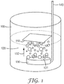
- a gas dispersion fritted disc gas bubbler 130 is immersed in an etching solution 120.
- the bubble generating surface 131 e.g. of the fritted disc
- the bubble generating surface 131 generally comprises small openings (i.e. pores not shown) formed as the result of a partial sintering process for particles (e.g., fritted glass or powder metallurgy product) or by machining a solid material (e.g., laser perforation or electro discharge machining).
- a tube 140 connected to a source of compressed gas, for example an air compressor (not shown), forces air through the openings emitting bubbles into the liquid etchant.
- the gas e.g., air
- the gas pressure can be controlled by a gas regulator and the air flow rate can be monitored (and controlled, as in the case of a rotameter with integrated needle valve) by the flow meter.
- One suitable gas dispersion fritted disc is available from Sigma-Aldrich, catalog number CLS3952530C. Such gas bubbler has an angle of 90° between the gas feed tube and the bubble generating surface of the fritted glass disc.
- Bubbles emitted from a bubble generating surface move (e.g. ascend) through the etchant bath in a direction 132 substantially normal to the metalized surface.
- the bubbles impinge upon the SAM printed metalized surface.
- the metalized substrate surface comprising the patterned SAM 110 is preferably positioned substantially parallel to the bubble generating surface. In doing so, the center region and edge regions of the SAM patterned substrate are about equidistance from the bubble generating surface.
- the pattern feature uniformity and the etch rate can be affected by a number of factors.
- the size of the gas bubbles is generally relatively small (e.g. 0.5 to 1 millimeter) at the surface of the SAM patterned substrate.
- some of these tiny gas bubbles can become pinned at certain locations on the metalized substrate.
- the etched surfaces can become heterogeneous and the areas not covered by bubbles etched more rapidly than those areas covered by bubbles. After etching, the unpatterned metal regions covered by the bubbles can remain on the substrate.
- a e.g.
- bubble generating surface with a pore size of at least 40, 50, or 60 micrometers can produce larger bubbles, having a diameter under some conditions of at least about 2 or 3 mm, at the surface of the SAM patterned substrate.
- the diameter of the bubbles ranged form about 2 to 4 mm.
- Such larger bubbles tend to coalesce and remain mobile upon reaching the SAM patterned substrate, rather than becoming pinned.
- the preferred maximum bubble size is surmised to be approximately 5 mm to 10 mm.
- the distance between the bubble generating surface and the SAM patterned metalized substrate is less than a certain value, for example 20 millimeters, the space for the bubbles to be agitated (e.g. laterally) along and then away from the surface is limited. This can also cause some gas bubbles to become pinned at certain locations on the surface of metalized substrate.
- the distance between the SAM patterned surface and bubble generating surface was increased, e.g. to at least 50 millimeters (e.g. for a 7.5 X 7.5 cm sample), substantially no metal residue associated with pinned bubbles was observed.
- the distance between the surface of the bubbling generating surface (e.g. of the fritted disc) and the SAM patterned surface of the substrate is typically at least 10 millimeter. In some embodiments, the distance is greater than 20 millimeter, and more typically at least 30 millimeter, 40 millimeter, or 50 millimeters.
- the size of the bubble generating surface (e.g. of the fritted disc) and the liquid etchant vessel can be selected based on the sample size of the SAM patterned substrate.
- the vessel is sufficiently large enough to accommodate the substrate.
- the size of the bubble generating surface is at least about one third of the size of the SAM patterned area of the substrate.
- the size of the bubble generating surface (e.g. of the gas dispersion fritted disc) is preferably at least about 3 cm in diameter (bubbler surface area equals 7.1 square centimeters) for a 7.5 cm x 7.5 cm SAM patterned substrate (substrate area equals 56.25 square centimeters).
- the etchant is not uniformly agitated. Rather, the gas bubbles primarily agitate the middle region of the etchant bath. This can result in the middle region of the SAM patterned metalized substrate being etched more rapidly than the edge region.
- the geometry of the bubble generating surface is similar to the geometry of the vessel. Hence, whereas a circular shaped bubble generating surface is preferred for a cylindrical etchant bath vessel; a rectangular shaped bubble generating surfaces is generally preferred for a rectangular shaped etchant bath in order to have uniform agitation throughout the etchant bath.
- the surface velocity is the volumetric air flow rate for the bubbles (volume per unit time) divided by the cross sectional area of the zone of rising bubbles.
- the cross sectional area of the zone of rising bubbles is approximated as the projected area of the bubbler surface that emits bubbles (pores plus any material between pores) onto a plane normal to the bubble flow direction.
- the air flow rate is low, there are fewer bubbles per unit time and the velocity of the bubbles as the bubbles are emitted from the bubble generating surface is relatively slow.
- the etch rate can at least double in comparison to the observed rate when no bubbling gas agitation at all is used.
- a surface velocity of about 50 cm/min can at least triple the etch rate (e.g. to at least 100 nm/min).
- the air flow rate is high, more bubbles are generated per unit time and the velocity of the bubbles is faster.
- the higher velocity is amenable to continuous circulation of the etching solution.
- the % bubble coverage at the SAM patterned metalized substrate surface is typically at least 30%, 40% or 50% and typically no greater than about 70 percent.
- the bubbles either coalesce upon colliding with the SAM patterned substrate surface or are swept away (e.g. laterally) from the surface, thereby preventing the bubbles from being pinned and retained on the SAM patterned metalized surface.
- the etch rate has been found to increase with increasing surface velocity (e.g. as created by increasing volumetric air flow rate) until the velocity reaches about 100 cm/min to 150 cm/min. Thereafter, for some etching setups, increasing the air flow and velocity does not substantially further increase the etch rate.
- increasing the air flow and velocity does not substantially further increase the etch rate.
- the bubbles can lift an unsupported SAM patterned metalized substrate upward and away from the etchant bath chemistry. This can also result in non-uniform etching.
- the distance between the bubble generating surface and the SAM patterned metalized substrate maximum as well as the velocity of the bubble when emitted form the bubble generating surface could be considerably higher for larger sized substrates and still fall within the scope of the invention.
- the etchant bath may be agitated with bubbling gas in combination with agitation provided by another method.
- the etchant bath may additionally be agitated such as provided by stirring, flowing, and/or ultrasonically activating the etch bath.
- ultrasonic activation employs relatively low amounts of ultrasonic energy and thus does not necessarily generate appreciable bubbling.
- the movement of the substrate may provide additional agitation such as provided by shaking, translating, rotating, and/or vibrating the substrate.
- the etch rate in the thickness direction for a metal coating can exceed 300 nm/minute.
- etch rate refers to the average etch rate given by dividing the thickness of metallization by the time required for the etchant to remove the metal.
- the etchant e.g., the oxidizing agent and metal complex forming molecule
- the etchant is typically washed away from the surface of the etched microcontact printed metal pattern.
- the etchant e.g., the oxidizing agent and metal complex forming molecule
- it is intended to completely remove the etchant it is not uncommon for very small concentrations of the wet etchant components to remain.
- the presence of such wet etchant components can be determined by various quantitative and/or qualitative analysis such as surface-enhanced Raman scattering, X-ray photoelectron spectroscopy, Auger electron spectroscopy, secondary ion mass spectrometry, and reflectance infrared spectroscopy.
- the method described herein can be conducted batch-wise or in a continuous process.
- the etched SAM-patterned metal pattern (corresponding to the raised features) can include a variety of patterns.
- the conductive patterns or pattern regions are generally contiguous and electrically conductive in the plane of the pattern.
- Preferred (e.g. conductive) patterns include regions with two dimensional meshes, e.g. square grids, rectangular (non-square) grids, or regular hexagonal networks, where conductive pattern features such as patterned lines define enclosed open areas within the mesh.
- the open spaces defined by the metal patterns can be defined as cells.
- Other useful geometries for mesh cells include random cell shapes and irregular polygons.
- the patterns can be described with reference to the total surface area of open spaces.
- the pattern has an open area of at least 60%, 70%, 80%, 90%, 91%, 92%, 93%, 94%, or 95%.
- the pattern has an open area of at least 96%, 97%, or 98%. The remainder is the total surface area of the patterned metal.
- the width of the patterned features can vary depending on the pattern selection.
- the line width is typically at least 0.5 microns and no greater than 20 microns.
- the patterned feature e.g. line width
- the patterned feature ranges from 1 to 5 micrometers.
- the method described herein is amenable to producing patterned articles comprising an etched microcontact printed metal pattern good pattern uniformity for an area of at least 25 cm 2 .
- the etched microcontact printed metal pattern exhibits good pattern uniformity for an area of at least 100cm 2 , in some embodiments at least 150cm 2 , and in yet other embodiments at least 200cm 2 .
- the uniformity of a pattern feature can be evaluated according to various methods.
- the pattern feature uniformity as described herein is determined by measuring the (e.g. shortest) dimension of a repeating pattern feature from the middle region (e.g. at or near the center) of the metal pattern and measuring the dimension of that (i.e. same) repeating pattern feature at an edge region (e.g. at or near the perimeter) of the pattern.
- the pattern comprises an array of linear pattern features forming a metal mesh pattern such as open (e.g. hexagonal) cells the line width of traces that defines the edges of cells from the middle region of the patterned substrate can be subtracted from the line width of cells from an edge region. If there is no difference in pattern (e.g. line width) feature dimension, the pattern feature uniformity is 100%.
- % Uniformity (1 - (Absolute Value of Difference in Feature Dimension Between Middle Region and Edge Region/(Greater of the Feature Dimensions for the Middle Region and Edge Region))) X 100
- the greater feature (e.g. line width) dimension is typically the feature (e.g. line width) dimension at the edge.
- the greater feature (e.g. line width) dimension can also be the middle (e.g. line width) dimension.
- the uniformity of repeating filled pattern features such as dots and squares can be evaluated in substantially the same manner by measuring area linear dimension of the repeating pattern features (e.g., edge width of a square, diameter of a circular dot).
- the pattern uniformity can alternatively be determined by comparing the metal pattern features to the raised feature (e.g. of the inked stamp) from which the pattern feature were derived from. This is commonly known as the pattern replication fidelity. The aforementioned comparison would be executed for different regions (e.g., edge region vs. middle region) of the substrate.
- the pattern feature uniformity throughout the area can generally be determined from comparing a single pattern feature measurement from the middle and edge region. This is especially true for repeating patterns (e.g. having the same design, thickness, and (e.g. line) width) throughout the metal patterned area. However, for larger metal patterned areas and those having multiple designs, a statistically meaningful number of pattern features measurements would be made to arrive at an average pattern feature uniformity. In the case of (e.g. repeating) metal patterned areas having an area greater than 75 cm 2 for example, a different procedure can be used to determine the % uniformity.
- each measurement is separated by a distance of at least about 4 to 5 cm.
- metal patterned articles described herein have a pattern feature uniformity of at least 80%, or 90% for an area of at least 25 cm 2 .
- a pattern feature uniformity of at least 95%, 96%, 97%, 98%, 99%, or 100% was obtained for various metal pattern thicknesses. In preferred embodiments, such pattern uniformity can be obtained for even larger total metal patterned areas.
- the total metal patterned area, particularly of silver or gold, may be at least 50 cm 2 , 100 cm 2 , 150 cm 2 , 200 cm 2 or greater.
- metal e.g. of silver and gold
- metal patterned articles described herein have increased metal pattern thicknesses.
- the thickness is at least 125 nm, 150 nm, 175 nm or 200 nm.
- the thickness of a silver or gold metal pattern may be at least 250 nm, 300 nm, 350 nm, 400 nm, or greater.
- Silver patterns (e.g. that also exhibit good uniformity) may have a thickness of at least 500 nm, 600 nm, 700 nm, 800 nm, 900 nm, 1000 nm, or greater.
- the methods and embodiments described here are particularly useful for achieving etched SAM-patterned metal patterns with the aforementioned thickness values and with the aforementioned pattern feature uniformity values.
- Increasing the thickness of the metal pattern is also amenable to narrower in-plane feature dimensions such as line width and/or lower area fraction coverage, for a given target level of conductance along the line.
- a mesh pattern having a 2 micrometer line width and 98% metal coverage has the same sheet resistance as a 1 micrometer line width and 99% metal coverage if the metal thickness is increased from 100 to 200 nanometers, respectively.
- Reducing the line width and/ metal coverage is amenable to improved optical properties such as higher light transmission and lower haze for low density mesh patterns.
- Metalized polymer film substrates were prepared by thermal evaporation of metal onto 0.127 mm (5 mil) polyethyleneterephthalate "PET" (ST504, E. I. DuPont de Nemours and Company, Wilmington, Delaware).
- PET polyethyleneterephthalate
- the substrate surface was coated with 30, 60, 100, and 125 nanometers of silver; 30 angstroms of chromium and then coated with 200, 500, 700, 1000 nanometers of silver; or 30 angstroms of titanium and then coated with 300 and 400 nanometers of silver.
- the gold-coated substrate was first coated with 30 angstroms of chromium and then coated with 400 nanometers of gold.
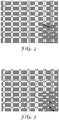
- FIG. 3 is an optical photomicrograph of a region of a completed pattern (thin film silver on PET), illustrating generally the geometry of low-density mesh region (hexagonal cell geometry with 97 percent open area and 3 micrometer wide lines forming hexagons).
- An elastomeric stamp was molded against the master tool by pouring uncured polydimethylsiloxane (PDMS, SylgardTM 184, Dow Corning, Midland Michigan) over the tool to a thickness of approximately 3.0 millimeters.
- PDMS polydimethylsiloxane
- the uncured silicone in contact with the master was degassed by exposing to a vacuum, and then cured for 2 hours at 70°C.
- a PDMS stamp was provided with a relief pattern comprising raised features approximately 1.8 micrometers in height.
- the raised features of the stamp were the lines defining the respective mesh geometry.
- the stamp was cut to a size of approximately 7 by 7 centimeters. This stamp is referred to as "Stamp 1".
- Example 11 a second master tool was prepared similarly to the first master tool, except that the pattern of photoresist was disposed on a plate of glass.
- the pattern of photoresist included the similar geometric elements (hexagonal mesh) described above for the first master tool, except that hexagonal cell geometry has 98 percent open area and 2 micrometer wide lines forming hexagons.
- the stamp was cut to a size of approximately 15 by 15 centimeters. This stamp is referred to as "Stamp 2".
- Stamp 1 was inked by contacting its back side (flat surface without relief pattern) to a solution of 5mM octadecylthiol ("ODT" O0005, TCI AMERICA, Wellesley Hills, Massachusetts) in ethanol for 20 hours.
- OHT octadecylthiol
- Stamp 2 was inked by contacting its back side (flat surface without relief pattern) to a solution of 10mM octadecylthiol in ethanol for 20 hours.
- Metalized polymer film substrates were stamped with the described inked stamp.
- stamping the metalized film was contacted to the stamp relief patterned-surface, which was faced up, by first contacting an edge of the film sample to the stamp surface and then rolling the film into contact across the stamp, using a roller with diameter of approximately 3.0 centimeters. The rolling step required less than 5 second to execute.
- the substrate was contacted with the stamp for 10 seconds for Stamp 1 and 15 second for Stamp 2 (of Example 11). Then, the substrate was peeled from the stamp, a step that required less than 1 second.
- the metalized film substrate with the SAM-printed pattern was placed in the etch bath for selective etching and metal patterning.
- an etchant solution was prepared by combining 2.25 grams of thiourea (T8656, Sigma-Aldrich, St. Louis, Missouri), 8.2 grams of ferric nitrate (216828, Sigma-Aldrich, St. Louis, Missouri), and 1000 milliliter of deionized water.
- the etchant was prepared by combining 4.5 grams of the thiourea, 16.4 grams of the ferric nitrate, and 1000 milliliter of deionized water.
- the etchant comprised 9.0 grams of the thiourea, 32.8 grams of the ferric nitrate, and 4000 milliliters of deionized water.
- Example 1 the samples were etched in an etchant bath having bubbling agitation, as depicted in FIG. 1 .
- the temperature of the etching solution was 21°C.
- One of two different gas bubblers was immersed into the etching solution and situated on the bottom of the beaker.
- the bubblers were all of a fritted glass disc type.
- the bubbler feed tube was connected with an air supply through a flow meter.
- the air pressure was controlled by a gas regulator and was set at 0.544 atm (8 psi).
- the air flow rate was monitored by the flow meter (LINDE FM 4334, Union Carbide, New York, bought by Dow Chemical in 1999).
- the SAM-printed metalized substrate was placed on the surface of the etching solution with metal side facing down (floating atop the etchant bath, as caused by surface tension).
- the distance between the surface of the fritted disc and the surface of the substrate was 70 millimeters (i.e., the travel distance of gas bubbles from the bubbler to the substrate surface was 70 millimeters).
- the gas bubbles were generated through the gas dispersion fritted disc and flowed up to hit the metal surface for agitating the etch process. Gas bubbles travelled in a direction generally normal to the surface of SAM-printed metalized substrate and were provided continuously. Examples 1-7 are reference examples which do not fall under the wording of the claims.
- Examples 1-10 samples with a size less than 7 centimeters by 7 centimeters, employed 1 liter of etching solution in a 2 liter beaker (i.e._14 centimeters in diameter) as an etchant bath.
- a gas dispersion fritted disc with a pore size of 40 ⁇ 60 micrometers and a disc diameter of 30 millimeters was used to generate gas bubbles, and the flow rate was set at 1100cc/min (i.e.155.7cm/min face velocity).
- the bubble size at the substrate surface was about 2 to 3 millimeters.
- the bubble density at the substrate surface was estimated to be about 70%.
- the velocity of the rising bubbles was greater than 40cm/s.
- Example 11 having a sample size of 15 centimeters by 15 centimeters, 4 liters of etching solution in a cylindrical etch bath (25 centimeters in diameter and 25 centimeters in height) was utilized. A gas dispersion fritted disc with a pore size of 170 ⁇ 220 micrometers and a disc diameter of 10 centimeters was used to generate gas bubbles, and the flow rate was set at 12222cc/min (i.e., 155.7cm/min face velocity). The bubble size at the substrate surface was about 2 to 4 millimeters. The bubble density at the substrate surface was estimated to be higher than 80%. The velocity of the rising bubbles was greater than 40cm/s.
- etching solution 1 liter was provided in a 2 liter beaker as the etchant bath.
- the etching solution was stirred with a (8 centimeter in length and 1.3 cm in diameter) magnetic stir bar at a rate of about 260 rpm.
- the sample was immersed into the solution and positioned vertically along the wall of the beaker.
- the etch time was recorded by VWR Big-Digit Stopwatch.
- the average etch rate of each sample was calculated by dividing the metal thickness by the etch time.
- the metal patterns were characterized using an optical microscope (Leica DFC 420, Leica Microsystems Inc., Bannockburn, Illinois). The microscopic techniques were used to determine the width of line features of the metal pattern. The pattern feature uniformity was determined as previously described.
- Hexagonal mesh pattern of thin film metal were fabricated and characterized as described above.
- the metal thickness, etch times, etch rate, line width at the edge and middle of the sample as well as the etch uniformity are reported in following Table 1 and 2.
- FIG. 2 is an optical photomicrograph of Example C-3, illustrating the line width at the edge region of the metalized pattern.
- FIG. 3 is an optical photomicrograph of Example C-3 illustrating the line width at the center region of the metalized pattern.
- Example C-4 was prepared in the same manner as Example C-1, except the following differences.
- the thickness of thin film silver was 100 nanometers.
- the silver substrate (7.5cm x 7.5cm) with printed pattern was placed on the surface of the etching solution with metal side facing down.
- the etching solution was stirred with a magnetic stirring bar at a rate of 260 revolution per minute for agitating the etch process.
- the edge region of the sample was completely etched, but the middle region of the sample remained unetched because vortex formed in the etching solution at this stirring speed, causing the etchant solution not to contact the metalized and SAM printed substrate surface in the middle region of the sample.
- % Uniformity (1- (Absolute Value of Difference in Feature Dimension Between Middle Region and Edge Region/(Greater of the Feature Dimensions for the Middle Region and Edge Region))) X 100
- Metalized polymer film substrates were prepared by sputter coating silver on polyetyleneterephthalate "PET" films (obtained from E.I. DuPont de Nemours Company, Wilmington, Delaware under trade name TEIJIN ST504) in a R2R system.
- PET polyetyleneterephthalate
- the polymer film substrates were coated to a thickness of 70 nanometers of silver or 120 nanometers of silver.
- the silver coated films were then printed with a self-assembling molecular (SAM) layer in a pattern according to methods described in US2009/218310 .
- SAM self-assembling molecular
- the etching solution consisted of 0.05M Ferric Nitrate (ACS reagent grade, obtained from GFS Chemicals, Powell, OH) and 0.1M Thiourea (ACS reagent grade, obtained from GFS Chemicals, Powell,OH) in deionized water.
- An aqueous processing unit (ASI Model 1024, commercially available from Eidschun Engineering, Clearwater, Fl, USA) equipped with an unwind station, a series of idlers configured to present the web in a face down orientation just under the liquid surface level within the processing unit and a winding unit was used.
- the winders and unwinders used were similar to those commercially available form Northfield Automation, Northfield, MN.
- the processing system (with multiple sumps and cavities) was modified mechanically to provide a partial immersion web path, allowing entry into and out of each sump or cavity.
- the main cavity allowed for 15 cm center-to-center spacing of the rollers in the immersion configuration.
- the rollers were 7 cm in diameter.
- the approximate length of web immersed was 22.5 cm.
- the mechanical modifications allowed the connection of a web system within each internal section of the system including the entry, main sump cavity, first rinse cavity, and drying section. The connection was created by attaching threaded pipe to the lower fluid delivery manifold inlets and the spray bar hangars on the side plate opposing the inlet from the manifold.
- the system was setup to provide bath agitation within the sump using 3 sparging tubes and one spray bar set at the top center of the main sump cavity ( ⁇ 132 L).
- the sparging tubes were connected to the lower manifold to keep from having static portions of the sump.
- the sparging tubes keep all the fluid agitated and the volume relatively homogeneous.
- the sparging tubes are polyproylene 1.27 cm (1/2") OD tubing fed, there are three. One pointed to each far corner of the sump (2) and one used to move the fluid toward the recirulating pump. The visible backwash from the farside of the sump exhibited good mixing across the whole sump.
- the spray bar on top was only used to move fluid through the sump cavity, no etching from the spray bar was likely since it is directed at the uncoated side of the web. All other manifold inlets were blocked off to prevent further flow.
- an Exair air knife 45 cm long, model# 110018, 316 stainless steel, commercially available from Exair, Inc., Cincinnati, OH
- the air knife was affixed to the already present stainless hardware used to cool and heat the sump. It was affixed using nylon zip ties in a temporary fashion.
- the air knife was laid in a perpendicular orientation to the web path.
- the first rinse sump incorporated the use of one set of spray bars to aid in an agitated rinse presented onto the backside of the web after leaving the etch sump and the web was immersed in the rinse solution to rinse the front side or patterned side of the web.
- the silver coated film web with the SAM-printed pattern was set on the core chuck of the unwind station and spliced to the previously unwound web material.
- the thiourea concentrate was added to the main sump and allowed to mix for 15 minutes using the pumping system available with the system. After mixing for 15 minutes, the ferric nitrate concentrate was added and allowed to mix via recirculation for 15 minutes.
- the web feed was initiated, the bubbles were turned on with an approximate air flow of 40 Lpm, observed via a Dwyer flow meter (Dwyer Instruments, Inc., Michigan City, IN).
- the web feed rate for etching was approximately 0.5 meters per minute (MPM) (1.75 feet per minute, FPM) for ⁇ 70 nm thick Ag film and 0.4 MPM (1.25 FPM) for ⁇ 120 nm thick film.
- the estimated etch time was 27 seconds for film with 70 nm of silver and 38 seconds for film with 120 nm of silver.
- the etch rate were 156 nm/min and 189 nm/min for films with 70 nm of silver and 120 nm of silver, respectively. Percentage of etching uniformity for these two samples is 90% as determined by the equation previously described.
Landscapes
- Chemical & Material Sciences (AREA)
- Engineering & Computer Science (AREA)
- Chemical Kinetics & Catalysis (AREA)
- General Chemical & Material Sciences (AREA)
- Materials Engineering (AREA)
- Mechanical Engineering (AREA)
- Metallurgy (AREA)
- Organic Chemistry (AREA)
- Manufacturing & Machinery (AREA)
- Microelectronics & Electronic Packaging (AREA)
- ing And Chemical Polishing (AREA)
- Weting (AREA)
Claims (12)
- Verfahren zum Strukturieren eines Substrats, das aufweist:Bereitstellen eines Substrats, aufweisend eine metallisierte Oberfläche, die einen strukturierten Bereich einer selbstorganisierten Monoschicht und einen unstrukturierten Bereich aufweist; undNassätzen des Substrats mit einer Geschwindigkeit von mindestens 300 nm/Minute, um Metall von dem unstrukturierten Bereich zu entfernen, wodurch eine Metallstruktur gebildet wird;wobei das Nassätzen das Eintauchen der metallisierten Oberfläche, die den strukturierten Bereich einer selbstorganisierten Monoschicht aufweist, in ein flüssiges Ätzmittel, das mit Sprudelgas bewegt wird, aufweist, wobei sich Blasen, die von einer Blasenerzeugungsoberfläche abgegeben werden, durch das flüssige Ätzmittel in einer Richtung im Wesentlichen senkrecht zu der metallisierten Oberfläche bewegen und die Blasen auf dem strukturierten Bereich einer selbstorganisierten Monoschicht auftreffen, wobei die metallisierte Oberfläche in einem Abstand von mindestens 30 Millimetern von der Blasenerzeugungsoberfläche angeordnet ist, wobei die Blasenerzeugungsoberfläche eine Fläche von mindestens ungefähr einem Drittel von der der metallisierten Oberfläche, die den strukturierten Bereich einer selbstorganisierten Monoschicht aufweist, hat, wobei Blasen, die von der Blasenerzeugungsoberfläche abgegeben werden, eine Geschwindigkeit von mindestens 10 cm/min aufweisen, und wobei die Blasen einen Durchmesser von mindestens 2 Millimetern an der metallisierten Oberfläche aufweisen.
- Verfahren nach Anspruch 1, wobei der strukturierte Bereich einer selbstorganisierten Monoschicht auf die metallisierte Oberfläche mikrokontaktgedruckt wird.
- Verfahren nach Anspruch 2, wobei der strukturierte Bereich einer selbstorganisierten Monoschicht durch Bereitstellen eines Tinte tragenden elastomeren Stempels, der selbstorganisierende Monoschicht bildende Moleküle umfasst, mikrokontaktgedruckt wird; und
Inkontaktbringen des Tinte tragenden Stempels mit einem metallbeschichteten Substrat;
wobei der elastomere Stempel und/oder das Substrat eine oder mehrere erhöhte Merkmale aufweist, die den strukturierten Bereich einer selbstorganisierten Monoschicht bilden. - Verfahren nach einem der vorstehenden Ansprüche, wobei die metallisierte Oberfläche, die den strukturierten Bereich einer selbstorganisierten Monoschicht und den unstrukturierten Bereich aufweist, im Wesentlichen parallel zu einer Blasenerzeugungsoberfläche, die Blasen abgibt, angeordnet ist.
- Verfahren nach einem der vorstehenden Ansprüche, wobei die Monoschicht eine organische Schwefelverbindung aufweist.
- Verfahren nach Anspruch 5, wobei die organische Schwefelverbindung ein Alkylthiol aufweist.
- Verfahren nach einem der vorstehenden Ansprüche, wobei das Ätzmittel Eisen(III)-lonen aufweist.
- Verfahren nach einem der vorstehenden Ansprüche, wobei das Ätzmittel Thioharnstoff oder ein Thioharnstoffderivat aufweist.
- Verfahren nach einem der vorstehenden Ansprüche, wobei das Metall aus Silber oder Gold ausgewählt ist.
- Metallischer strukturierter Artikel, aufweisend:
ein Substrat und eine geätzte mikrokontaktgedruckte Metallstruktur, die auf dem Substrat angeordnet ist, wobei die Struktur eine Dicke von mindestens 100 Nanometern und eine Strukturmerkmal-Gleichmäßigkeit von mindestens 75 % über eine Fläche von mindestens 25 cm2 aufweist, wobei die Strukturmerkmal-Gleichmäßigkeit unter Verwendung eines optischen Mikroskops durch Messen der kürzesten Abmessung eines sich wiederholenden Strukturmerkmals von einem Mittelbereich in der Mitte der Metallstruktur und Messen der Abmessung des gleichen sich wiederholenden Strukturmerkmals an einem Randbereich am Umfang der Struktur bestimmt wird, wobei die Differenz zwischen den Abmessungen der Strukturmerkmale verwendet wird, um eine Strukturmerkmal-Gleichmäßigkeit gemäß der folgenden Gleichung zu berechnen: % Gleichmäßigkeit = (1 - (absoluter Wert der Differenz der kürzesten Merkmalabmessung zwischen Mittelbereich und Randbereich/(größere der kürzesten Merkmalabmessungen für den Mittelbereich und Randbereich))) x 100. - Metallischer strukturierter Artikel nach Anspruch 10, wobei die Struktur eine Strukturmerkmal-Gleichmäßigkeit von mindestens 90 % aufweist.
- Metallischer strukturierter Artikel nach einem der Ansprüche 10-11, wobei das Metall Silber oder Gold aufweist.
Applications Claiming Priority (2)
| Application Number | Priority Date | Filing Date | Title |
|---|---|---|---|
| US22040709P | 2009-06-25 | 2009-06-25 | |
| PCT/US2010/038942 WO2010151471A1 (en) | 2009-06-25 | 2010-06-17 | Methods of wet etching a self-assembled monolayer patterned substrate and metal patterned articles |
Publications (2)
| Publication Number | Publication Date |
|---|---|
| EP2446067A1 EP2446067A1 (de) | 2012-05-02 |
| EP2446067B1 true EP2446067B1 (de) | 2019-11-20 |
Family
ID=42710497
Family Applications (1)
| Application Number | Title | Priority Date | Filing Date |
|---|---|---|---|
| EP10728512.4A Active EP2446067B1 (de) | 2009-06-25 | 2010-06-17 | Verfahren zur nassätzung eines selbstanordnenden einschichtigen strukturierten substrats und metallstrukturierte artikel |
Country Status (5)
| Country | Link |
|---|---|
| US (1) | US8647522B2 (de) |
| EP (1) | EP2446067B1 (de) |
| JP (3) | JP6128847B2 (de) |
| CN (1) | CN102803562B (de) |
| WO (1) | WO2010151471A1 (de) |
Families Citing this family (15)
| Publication number | Priority date | Publication date | Assignee | Title |
|---|---|---|---|---|
| US8970515B2 (en) | 2009-02-26 | 2015-03-03 | 3M Innovative Properties Company | Touch screen sensor and patterned substrate having overlaid micropatterns with low visibility |
| EP2449547B1 (de) | 2009-06-30 | 2016-09-21 | 3M Innovative Properties Company | Elektronische anzeigen und mikrostrukturierte metallsubstrate mit einer grafik |
| WO2011079032A1 (en) | 2009-12-22 | 2011-06-30 | 3M Innovative Properties Company | Apparatus and method for microcontact printing using a pressurized roller |
| EP2652837A4 (de) | 2010-12-16 | 2014-07-30 | 3M Innovative Properties Co | Transparente mikrostrukturierte rfid-antenne und diese enthaltende artikel |
| US9301397B2 (en) | 2011-09-30 | 2016-03-29 | 3M Innovative Properties Company | Methods of continuously wet etching a patterned substrate |
| SG11201603375TA (en) | 2013-11-06 | 2016-05-30 | 3M Innovative Properties Co | Microcontact printing stamps with functional features |
| WO2015126372A1 (en) * | 2014-02-19 | 2015-08-27 | Uni-Pixel Displays, Inc. | Method of passivating a conductive pattern with self-assembling monolayers |
| US9232661B1 (en) | 2014-09-22 | 2016-01-05 | International Business Machines Corporation | Magnetically controllable fluidic etching process |
| CN104538138B (zh) * | 2014-12-30 | 2017-12-29 | 南京萨特科技发展有限公司 | 精密贴片电阻器的制作方法 |
| CN104630773B (zh) * | 2015-03-07 | 2017-01-18 | 宋彦震 | 一种全自动pcb板腐蚀箱 |
| CN106455348A (zh) * | 2016-11-29 | 2017-02-22 | 福建农林大学 | Pcb板升降腐蚀机及使用方法 |
| CN107833827B (zh) * | 2017-10-25 | 2020-07-31 | 武汉华星光电技术有限公司 | 一种阵列基板的刻蚀方法 |
| JP7368264B2 (ja) | 2019-02-20 | 2023-10-24 | 株式会社Screenホールディングス | 基板処理装置、及び基板処理方法 |
| CN113463099B (zh) * | 2020-03-31 | 2023-08-29 | 长沙韶光铬版有限公司 | 一种银的细微图形化蚀刻方法 |
| FR3110716B1 (fr) * | 2020-05-19 | 2022-04-29 | Commissariat Energie Atomique | Procede de fabrication de moules pour lithographie par nano-impression |
Family Cites Families (26)
| Publication number | Priority date | Publication date | Assignee | Title |
|---|---|---|---|---|
| US1313233A (en) | 1919-08-12 | Ernest grass | ||
| GB1080536A (en) | 1964-09-18 | 1967-08-23 | Her Majesty S Principal Sec De | Improvements in or relating to chemical etching |
| US3483049A (en) | 1965-12-20 | 1969-12-09 | Teletype Corp | Method of froth etching |
| US3565707A (en) | 1969-03-03 | 1971-02-23 | Fmc Corp | Metal dissolution |
| DE2030304C3 (de) | 1970-06-19 | 1981-06-19 | Walter 6983 Kreuzwertheim Lemmen | Verfahren zum Ätzen von Metall |
| DE2353936A1 (de) | 1973-10-27 | 1975-05-07 | Rudolf Schmidt | Verfahren und vorrichtung zur verbesserung und/oder beschleunigung chemischer vorgaenge in fluessigkeiten und baedern |
| US4602184A (en) * | 1984-10-29 | 1986-07-22 | Ford Motor Company | Apparatus for applying high frequency ultrasonic energy to cleaning and etching solutions |
| JPS61133390A (ja) * | 1984-12-03 | 1986-06-20 | Hitachi Cable Ltd | めつきされた金の剥離方法 |
| JPS61207584A (ja) * | 1985-03-11 | 1986-09-13 | Sumitomo Electric Ind Ltd | 回路基板の製造方法 |
| JPH0719944B2 (ja) * | 1991-02-05 | 1995-03-06 | インターナショナル・ビジネス・マシーンズ・コーポレイション | 微細電子回路パッケージの製造方法 |
| JPH0677624A (ja) * | 1992-08-25 | 1994-03-18 | Matsushita Electric Ind Co Ltd | プリント配線板のエッチング方法とエッチング装置 |
| US6518168B1 (en) | 1995-08-18 | 2003-02-11 | President And Fellows Of Harvard College | Self-assembled monolayer directed patterning of surfaces |
| WO2002033461A2 (en) * | 2000-10-16 | 2002-04-25 | Ozin Geoffrey A | Method of self-assembly and optical applications of crystalline colloidal patterns on substrates |
| US7041232B2 (en) * | 2001-03-26 | 2006-05-09 | International Business Machines Corporation | Selective etching of substrates with control of the etch profile |
| US20020190028A1 (en) * | 2001-05-31 | 2002-12-19 | International Business Machines Corporation | Method of improving uniformity of etching of a film on an article |
| GB0323902D0 (en) * | 2003-10-11 | 2003-11-12 | Koninkl Philips Electronics Nv | Method for patterning a substrate surface |
| US20110104840A1 (en) * | 2004-12-06 | 2011-05-05 | Koninklijke Philips Electronics, N.V. | Etchant Solutions And Additives Therefor |
| JP4528164B2 (ja) * | 2005-03-11 | 2010-08-18 | 関東化学株式会社 | エッチング液組成物 |
| US8192795B2 (en) * | 2006-06-28 | 2012-06-05 | Northwestern University | Etching and hole arrays |
| US8764996B2 (en) | 2006-10-18 | 2014-07-01 | 3M Innovative Properties Company | Methods of patterning a material on polymeric substrates |
| US8284332B2 (en) | 2008-08-01 | 2012-10-09 | 3M Innovative Properties Company | Touch screen sensor with low visibility conductors |
| WO2009108771A2 (en) | 2008-02-28 | 2009-09-03 | 3M Innovative Properties Company | Methods of patterning a conductor on a substrate |
| JP2011514597A (ja) | 2008-02-28 | 2011-05-06 | スリーエム イノベイティブ プロパティズ カンパニー | 変化するシート抵抗を有するタッチスクリーンセンサ |
| KR101720919B1 (ko) | 2008-02-28 | 2017-03-28 | 쓰리엠 이노베이티브 프로퍼티즈 컴파니 | 터치 스크린 센서 |
| CN102307734B (zh) | 2008-12-11 | 2015-06-03 | 3M创新有限公司 | 图案化方法 |
| JP2015137927A (ja) * | 2014-01-22 | 2015-07-30 | 株式会社ブルービジョン | 撮像装置及び検査システム |
-
2010
- 2010-06-17 WO PCT/US2010/038942 patent/WO2010151471A1/en active Application Filing
- 2010-06-17 EP EP10728512.4A patent/EP2446067B1/de active Active
- 2010-06-17 US US13/319,704 patent/US8647522B2/en not_active Expired - Fee Related
- 2010-06-17 JP JP2012517584A patent/JP6128847B2/ja active Active
- 2010-06-17 CN CN201080028067.6A patent/CN102803562B/zh not_active Expired - Fee Related
-
2015
- 2015-07-09 JP JP2015137927A patent/JP6399975B2/ja not_active Expired - Fee Related
-
2017
- 2017-03-15 JP JP2017050042A patent/JP2017166070A/ja not_active Withdrawn
Non-Patent Citations (1)
| Title |
|---|
| None * |
Also Published As
| Publication number | Publication date |
|---|---|
| JP6128847B2 (ja) | 2017-05-17 |
| JP2017166070A (ja) | 2017-09-21 |
| EP2446067A1 (de) | 2012-05-02 |
| JP6399975B2 (ja) | 2018-10-03 |
| US8647522B2 (en) | 2014-02-11 |
| CN102803562B (zh) | 2015-09-30 |
| WO2010151471A1 (en) | 2010-12-29 |
| JP2012531518A (ja) | 2012-12-10 |
| US20120082825A1 (en) | 2012-04-05 |
| JP2015214757A (ja) | 2015-12-03 |
| CN102803562A (zh) | 2012-11-28 |
Similar Documents
| Publication | Publication Date | Title |
|---|---|---|
| EP2446067B1 (de) | Verfahren zur nassätzung eines selbstanordnenden einschichtigen strukturierten substrats und metallstrukturierte artikel | |
| EP2370269B1 (de) | Musterbildungsprozess | |
| Datta et al. | Electrochemical micromachining: An environmentally friendly, high speed processing technology | |
| JP5199089B2 (ja) | パターン化トポグラフィーの複製と自己組織化単一層を用いた微細加工 | |
| JP4662994B2 (ja) | パターン化トポグラフィおよび自己組織化モノレイヤーを用いる微細加工 | |
| US20060083927A1 (en) | Thermal interface incorporating nanotubes | |
| JP5319769B2 (ja) | パターン形成された基板の形成方法 | |
| US20120247355A1 (en) | Apparatus and method for microcontact printing using a pressurized roller | |
| US11006528B2 (en) | Methods of etching conductive features, and related devices and systems | |
| US8268400B2 (en) | Method and apparatus for producing conductive material | |
| JP6845146B2 (ja) | 装飾及び/又は機能用の金属パターンを基材上に製造する方法及び装置、当該製造方法を含む物品の生産方法及び使用される消耗品 | |
| US9301397B2 (en) | Methods of continuously wet etching a patterned substrate | |
| Bessueille et al. | Selective metal pattern fabrication through micro-contact or ink-jet printing and electroless plating onto polymer surfaces chemically modified by plasma treatments | |
| Zhang et al. | Control and Patterning of Various Hydrophobic Surfaces: In-situ Modification Realized by Flexible Atmospheric Plasma Stamp Technique | |
| JP3808037B2 (ja) | 基板上の金属の無電界堆積およびパターニングのための方法 | |
| CN115243799B (zh) | 涂覆方法 | |
| JP4783885B1 (ja) | ヘアライン燻し調ステンレス鋼板の製造方法及びヘアライン燻し調ステンレス鋼板 | |
| EP4299790A1 (de) | Verfahren zum ätzen eines kunststoffsubstrats einschliesslich sprühen und elektrolytische regeneration | |
| Yang et al. | Method for forming Cu metal wires by microdispensing pattern, Part I: self assembly treatment & the ink-jet process | |
| JP6848243B2 (ja) | 導電性基板の製造方法 | |
| Li et al. | Rapid Fabrication of High-Resolution Flexible Electronics via Nanoparticle Self-Assembly and Transfer Printing | |
| Huang et al. | Applications of thick Sacrificial-Layer of zinc in LIGA process |
Legal Events
| Date | Code | Title | Description |
|---|---|---|---|
| PUAI | Public reference made under article 153(3) epc to a published international application that has entered the european phase |
Free format text: ORIGINAL CODE: 0009012 |
|
| 17P | Request for examination filed |
Effective date: 20120104 |
|
| AK | Designated contracting states |
Kind code of ref document: A1 Designated state(s): AL AT BE BG CH CY CZ DE DK EE ES FI FR GB GR HR HU IE IS IT LI LT LU LV MC MK MT NL NO PL PT RO SE SI SK SM TR |
|
| DAX | Request for extension of the european patent (deleted) | ||
| STAA | Information on the status of an ep patent application or granted ep patent |
Free format text: STATUS: EXAMINATION IS IN PROGRESS |
|
| 17Q | First examination report despatched |
Effective date: 20170216 |
|
| GRAP | Despatch of communication of intention to grant a patent |
Free format text: ORIGINAL CODE: EPIDOSNIGR1 |
|
| STAA | Information on the status of an ep patent application or granted ep patent |
Free format text: STATUS: GRANT OF PATENT IS INTENDED |
|
| INTG | Intention to grant announced |
Effective date: 20190418 |
|
| GRAJ | Information related to disapproval of communication of intention to grant by the applicant or resumption of examination proceedings by the epo deleted |
Free format text: ORIGINAL CODE: EPIDOSDIGR1 |
|
| STAA | Information on the status of an ep patent application or granted ep patent |
Free format text: STATUS: EXAMINATION IS IN PROGRESS |
|
| INTC | Intention to grant announced (deleted) | ||
| GRAS | Grant fee paid |
Free format text: ORIGINAL CODE: EPIDOSNIGR3 |
|
| STAA | Information on the status of an ep patent application or granted ep patent |
Free format text: STATUS: GRANT OF PATENT IS INTENDED |
|
| GRAP | Despatch of communication of intention to grant a patent |
Free format text: ORIGINAL CODE: EPIDOSNIGR1 |
|
| GRAA | (expected) grant |
Free format text: ORIGINAL CODE: 0009210 |
|
| STAA | Information on the status of an ep patent application or granted ep patent |
Free format text: STATUS: THE PATENT HAS BEEN GRANTED |
|
| INTG | Intention to grant announced |
Effective date: 20191002 |
|
| AK | Designated contracting states |
Kind code of ref document: B1 Designated state(s): AL AT BE BG CH CY CZ DE DK EE ES FI FR GB GR HR HU IE IS IT LI LT LU LV MC MK MT NL NO PL PT RO SE SI SK SM TR |
|
| REG | Reference to a national code |
Ref country code: GB Ref legal event code: FG4D |
|
| REG | Reference to a national code |
Ref country code: CH Ref legal event code: EP |
|
| REG | Reference to a national code |
Ref country code: IE Ref legal event code: FG4D |
|
| REG | Reference to a national code |
Ref country code: DE Ref legal event code: R096 Ref document number: 602010062021 Country of ref document: DE |
|
| REG | Reference to a national code |
Ref country code: AT Ref legal event code: REF Ref document number: 1204285 Country of ref document: AT Kind code of ref document: T Effective date: 20191215 |
|
| REG | Reference to a national code |
Ref country code: NL Ref legal event code: MP Effective date: 20191120 |
|
| REG | Reference to a national code |
Ref country code: LT Ref legal event code: MG4D |
|
| PG25 | Lapsed in a contracting state [announced via postgrant information from national office to epo] |
Ref country code: SE Free format text: LAPSE BECAUSE OF FAILURE TO SUBMIT A TRANSLATION OF THE DESCRIPTION OR TO PAY THE FEE WITHIN THE PRESCRIBED TIME-LIMIT Effective date: 20191120 Ref country code: LV Free format text: LAPSE BECAUSE OF FAILURE TO SUBMIT A TRANSLATION OF THE DESCRIPTION OR TO PAY THE FEE WITHIN THE PRESCRIBED TIME-LIMIT Effective date: 20191120 Ref country code: GR Free format text: LAPSE BECAUSE OF FAILURE TO SUBMIT A TRANSLATION OF THE DESCRIPTION OR TO PAY THE FEE WITHIN THE PRESCRIBED TIME-LIMIT Effective date: 20200221 Ref country code: NO Free format text: LAPSE BECAUSE OF FAILURE TO SUBMIT A TRANSLATION OF THE DESCRIPTION OR TO PAY THE FEE WITHIN THE PRESCRIBED TIME-LIMIT Effective date: 20200220 Ref country code: BG Free format text: LAPSE BECAUSE OF FAILURE TO SUBMIT A TRANSLATION OF THE DESCRIPTION OR TO PAY THE FEE WITHIN THE PRESCRIBED TIME-LIMIT Effective date: 20200220 Ref country code: FI Free format text: LAPSE BECAUSE OF FAILURE TO SUBMIT A TRANSLATION OF THE DESCRIPTION OR TO PAY THE FEE WITHIN THE PRESCRIBED TIME-LIMIT Effective date: 20191120 Ref country code: ES Free format text: LAPSE BECAUSE OF FAILURE TO SUBMIT A TRANSLATION OF THE DESCRIPTION OR TO PAY THE FEE WITHIN THE PRESCRIBED TIME-LIMIT Effective date: 20191120 Ref country code: NL Free format text: LAPSE BECAUSE OF FAILURE TO SUBMIT A TRANSLATION OF THE DESCRIPTION OR TO PAY THE FEE WITHIN THE PRESCRIBED TIME-LIMIT Effective date: 20191120 Ref country code: LT Free format text: LAPSE BECAUSE OF FAILURE TO SUBMIT A TRANSLATION OF THE DESCRIPTION OR TO PAY THE FEE WITHIN THE PRESCRIBED TIME-LIMIT Effective date: 20191120 |
|
| PG25 | Lapsed in a contracting state [announced via postgrant information from national office to epo] |
Ref country code: IS Free format text: LAPSE BECAUSE OF FAILURE TO SUBMIT A TRANSLATION OF THE DESCRIPTION OR TO PAY THE FEE WITHIN THE PRESCRIBED TIME-LIMIT Effective date: 20200320 Ref country code: HR Free format text: LAPSE BECAUSE OF FAILURE TO SUBMIT A TRANSLATION OF THE DESCRIPTION OR TO PAY THE FEE WITHIN THE PRESCRIBED TIME-LIMIT Effective date: 20191120 |
|
| PG25 | Lapsed in a contracting state [announced via postgrant information from national office to epo] |
Ref country code: AL Free format text: LAPSE BECAUSE OF FAILURE TO SUBMIT A TRANSLATION OF THE DESCRIPTION OR TO PAY THE FEE WITHIN THE PRESCRIBED TIME-LIMIT Effective date: 20191120 |
|
| PG25 | Lapsed in a contracting state [announced via postgrant information from national office to epo] |
Ref country code: CZ Free format text: LAPSE BECAUSE OF FAILURE TO SUBMIT A TRANSLATION OF THE DESCRIPTION OR TO PAY THE FEE WITHIN THE PRESCRIBED TIME-LIMIT Effective date: 20191120 Ref country code: RO Free format text: LAPSE BECAUSE OF FAILURE TO SUBMIT A TRANSLATION OF THE DESCRIPTION OR TO PAY THE FEE WITHIN THE PRESCRIBED TIME-LIMIT Effective date: 20191120 Ref country code: PT Free format text: LAPSE BECAUSE OF FAILURE TO SUBMIT A TRANSLATION OF THE DESCRIPTION OR TO PAY THE FEE WITHIN THE PRESCRIBED TIME-LIMIT Effective date: 20200412 Ref country code: EE Free format text: LAPSE BECAUSE OF FAILURE TO SUBMIT A TRANSLATION OF THE DESCRIPTION OR TO PAY THE FEE WITHIN THE PRESCRIBED TIME-LIMIT Effective date: 20191120 Ref country code: DK Free format text: LAPSE BECAUSE OF FAILURE TO SUBMIT A TRANSLATION OF THE DESCRIPTION OR TO PAY THE FEE WITHIN THE PRESCRIBED TIME-LIMIT Effective date: 20191120 |
|
| REG | Reference to a national code |
Ref country code: AT Ref legal event code: MK05 Ref document number: 1204285 Country of ref document: AT Kind code of ref document: T Effective date: 20191120 |
|
| REG | Reference to a national code |
Ref country code: DE Ref legal event code: R097 Ref document number: 602010062021 Country of ref document: DE |
|
| PG25 | Lapsed in a contracting state [announced via postgrant information from national office to epo] |
Ref country code: SM Free format text: LAPSE BECAUSE OF FAILURE TO SUBMIT A TRANSLATION OF THE DESCRIPTION OR TO PAY THE FEE WITHIN THE PRESCRIBED TIME-LIMIT Effective date: 20191120 Ref country code: SK Free format text: LAPSE BECAUSE OF FAILURE TO SUBMIT A TRANSLATION OF THE DESCRIPTION OR TO PAY THE FEE WITHIN THE PRESCRIBED TIME-LIMIT Effective date: 20191120 |
|
| PLBE | No opposition filed within time limit |
Free format text: ORIGINAL CODE: 0009261 |
|
| STAA | Information on the status of an ep patent application or granted ep patent |
Free format text: STATUS: NO OPPOSITION FILED WITHIN TIME LIMIT |
|
| 26N | No opposition filed |
Effective date: 20200821 |
|
| PG25 | Lapsed in a contracting state [announced via postgrant information from national office to epo] |
Ref country code: AT Free format text: LAPSE BECAUSE OF FAILURE TO SUBMIT A TRANSLATION OF THE DESCRIPTION OR TO PAY THE FEE WITHIN THE PRESCRIBED TIME-LIMIT Effective date: 20191120 Ref country code: PL Free format text: LAPSE BECAUSE OF FAILURE TO SUBMIT A TRANSLATION OF THE DESCRIPTION OR TO PAY THE FEE WITHIN THE PRESCRIBED TIME-LIMIT Effective date: 20191120 Ref country code: SI Free format text: LAPSE BECAUSE OF FAILURE TO SUBMIT A TRANSLATION OF THE DESCRIPTION OR TO PAY THE FEE WITHIN THE PRESCRIBED TIME-LIMIT Effective date: 20191120 |
|
| REG | Reference to a national code |
Ref country code: DE Ref legal event code: R119 Ref document number: 602010062021 Country of ref document: DE |
|
| PG25 | Lapsed in a contracting state [announced via postgrant information from national office to epo] |
Ref country code: IT Free format text: LAPSE BECAUSE OF FAILURE TO SUBMIT A TRANSLATION OF THE DESCRIPTION OR TO PAY THE FEE WITHIN THE PRESCRIBED TIME-LIMIT Effective date: 20191120 Ref country code: MC Free format text: LAPSE BECAUSE OF FAILURE TO SUBMIT A TRANSLATION OF THE DESCRIPTION OR TO PAY THE FEE WITHIN THE PRESCRIBED TIME-LIMIT Effective date: 20191120 |
|
| REG | Reference to a national code |
Ref country code: CH Ref legal event code: PL |
|
| GBPC | Gb: european patent ceased through non-payment of renewal fee |
Effective date: 20200617 |
|
| PG25 | Lapsed in a contracting state [announced via postgrant information from national office to epo] |
Ref country code: LU Free format text: LAPSE BECAUSE OF NON-PAYMENT OF DUE FEES Effective date: 20200617 |
|
| REG | Reference to a national code |
Ref country code: BE Ref legal event code: MM Effective date: 20200630 |
|
| PG25 | Lapsed in a contracting state [announced via postgrant information from national office to epo] |
Ref country code: CH Free format text: LAPSE BECAUSE OF NON-PAYMENT OF DUE FEES Effective date: 20200630 Ref country code: IE Free format text: LAPSE BECAUSE OF NON-PAYMENT OF DUE FEES Effective date: 20200617 Ref country code: LI Free format text: LAPSE BECAUSE OF NON-PAYMENT OF DUE FEES Effective date: 20200630 Ref country code: GB Free format text: LAPSE BECAUSE OF NON-PAYMENT OF DUE FEES Effective date: 20200617 Ref country code: FR Free format text: LAPSE BECAUSE OF NON-PAYMENT OF DUE FEES Effective date: 20200630 |
|
| PG25 | Lapsed in a contracting state [announced via postgrant information from national office to epo] |
Ref country code: BE Free format text: LAPSE BECAUSE OF NON-PAYMENT OF DUE FEES Effective date: 20200630 Ref country code: DE Free format text: LAPSE BECAUSE OF NON-PAYMENT OF DUE FEES Effective date: 20210101 |
|
| PG25 | Lapsed in a contracting state [announced via postgrant information from national office to epo] |
Ref country code: TR Free format text: LAPSE BECAUSE OF FAILURE TO SUBMIT A TRANSLATION OF THE DESCRIPTION OR TO PAY THE FEE WITHIN THE PRESCRIBED TIME-LIMIT Effective date: 20191120 Ref country code: MT Free format text: LAPSE BECAUSE OF FAILURE TO SUBMIT A TRANSLATION OF THE DESCRIPTION OR TO PAY THE FEE WITHIN THE PRESCRIBED TIME-LIMIT Effective date: 20191120 Ref country code: CY Free format text: LAPSE BECAUSE OF FAILURE TO SUBMIT A TRANSLATION OF THE DESCRIPTION OR TO PAY THE FEE WITHIN THE PRESCRIBED TIME-LIMIT Effective date: 20191120 |
|
| PG25 | Lapsed in a contracting state [announced via postgrant information from national office to epo] |
Ref country code: MK Free format text: LAPSE BECAUSE OF FAILURE TO SUBMIT A TRANSLATION OF THE DESCRIPTION OR TO PAY THE FEE WITHIN THE PRESCRIBED TIME-LIMIT Effective date: 20191120 |