EP2434550A2 - Solarzelle und herstellungsverfahren dafür - Google Patents
Solarzelle und herstellungsverfahren dafür Download PDFInfo
- Publication number
- EP2434550A2 EP2434550A2 EP10827109A EP10827109A EP2434550A2 EP 2434550 A2 EP2434550 A2 EP 2434550A2 EP 10827109 A EP10827109 A EP 10827109A EP 10827109 A EP10827109 A EP 10827109A EP 2434550 A2 EP2434550 A2 EP 2434550A2
- Authority
- EP
- European Patent Office
- Prior art keywords
- substrate
- layer
- grooves
- pattern
- solar cell
- Prior art date
- Legal status (The legal status is an assumption and is not a legal conclusion. Google has not performed a legal analysis and makes no representation as to the accuracy of the status listed.)
- Withdrawn
Links
Images


Classifications
-
- H—ELECTRICITY
- H10—SEMICONDUCTOR DEVICES; ELECTRIC SOLID-STATE DEVICES NOT OTHERWISE PROVIDED FOR
- H10F—INORGANIC SEMICONDUCTOR DEVICES SENSITIVE TO INFRARED RADIATION, LIGHT, ELECTROMAGNETIC RADIATION OF SHORTER WAVELENGTH OR CORPUSCULAR RADIATION
- H10F71/00—Manufacture or treatment of devices covered by this subclass
-
- H—ELECTRICITY
- H10—SEMICONDUCTOR DEVICES; ELECTRIC SOLID-STATE DEVICES NOT OTHERWISE PROVIDED FOR
- H10F—INORGANIC SEMICONDUCTOR DEVICES SENSITIVE TO INFRARED RADIATION, LIGHT, ELECTROMAGNETIC RADIATION OF SHORTER WAVELENGTH OR CORPUSCULAR RADIATION
- H10F19/00—Integrated devices, or assemblies of multiple devices, comprising at least one photovoltaic cell covered by group H10F10/00, e.g. photovoltaic modules
- H10F19/30—Integrated devices, or assemblies of multiple devices, comprising at least one photovoltaic cell covered by group H10F10/00, e.g. photovoltaic modules comprising thin-film photovoltaic cells
-
- H—ELECTRICITY
- H10—SEMICONDUCTOR DEVICES; ELECTRIC SOLID-STATE DEVICES NOT OTHERWISE PROVIDED FOR
- H10F—INORGANIC SEMICONDUCTOR DEVICES SENSITIVE TO INFRARED RADIATION, LIGHT, ELECTROMAGNETIC RADIATION OF SHORTER WAVELENGTH OR CORPUSCULAR RADIATION
- H10F10/00—Individual photovoltaic cells, e.g. solar cells
- H10F10/10—Individual photovoltaic cells, e.g. solar cells having potential barriers
- H10F10/16—Photovoltaic cells having only PN heterojunction potential barriers
- H10F10/167—Photovoltaic cells having only PN heterojunction potential barriers comprising Group I-III-VI materials, e.g. CdS/CuInSe2 [CIS] heterojunction photovoltaic cells
-
- H—ELECTRICITY
- H10—SEMICONDUCTOR DEVICES; ELECTRIC SOLID-STATE DEVICES NOT OTHERWISE PROVIDED FOR
- H10F—INORGANIC SEMICONDUCTOR DEVICES SENSITIVE TO INFRARED RADIATION, LIGHT, ELECTROMAGNETIC RADIATION OF SHORTER WAVELENGTH OR CORPUSCULAR RADIATION
- H10F19/00—Integrated devices, or assemblies of multiple devices, comprising at least one photovoltaic cell covered by group H10F10/00, e.g. photovoltaic modules
- H10F19/30—Integrated devices, or assemblies of multiple devices, comprising at least one photovoltaic cell covered by group H10F10/00, e.g. photovoltaic modules comprising thin-film photovoltaic cells
- H10F19/31—Integrated devices, or assemblies of multiple devices, comprising at least one photovoltaic cell covered by group H10F10/00, e.g. photovoltaic modules comprising thin-film photovoltaic cells having multiple laterally adjacent thin-film photovoltaic cells deposited on the same substrate
- H10F19/35—Structures for the connecting of adjacent photovoltaic cells, e.g. interconnections or insulating spacers
-
- H—ELECTRICITY
- H10—SEMICONDUCTOR DEVICES; ELECTRIC SOLID-STATE DEVICES NOT OTHERWISE PROVIDED FOR
- H10F—INORGANIC SEMICONDUCTOR DEVICES SENSITIVE TO INFRARED RADIATION, LIGHT, ELECTROMAGNETIC RADIATION OF SHORTER WAVELENGTH OR CORPUSCULAR RADIATION
- H10F77/00—Constructional details of devices covered by this subclass
- H10F77/10—Semiconductor bodies
- H10F77/16—Material structures, e.g. crystalline structures, film structures or crystal plane orientations
- H10F77/169—Thin semiconductor films on metallic or insulating substrates
- H10F77/1696—Thin semiconductor films on metallic or insulating substrates the films including Group II-VI materials, e.g. CdTe or CdS
-
- H—ELECTRICITY
- H10—SEMICONDUCTOR DEVICES; ELECTRIC SOLID-STATE DEVICES NOT OTHERWISE PROVIDED FOR
- H10F—INORGANIC SEMICONDUCTOR DEVICES SENSITIVE TO INFRARED RADIATION, LIGHT, ELECTROMAGNETIC RADIATION OF SHORTER WAVELENGTH OR CORPUSCULAR RADIATION
- H10F77/00—Constructional details of devices covered by this subclass
- H10F77/10—Semiconductor bodies
- H10F77/16—Material structures, e.g. crystalline structures, film structures or crystal plane orientations
- H10F77/169—Thin semiconductor films on metallic or insulating substrates
- H10F77/1698—Thin semiconductor films on metallic or insulating substrates the metallic or insulating substrates being flexible
- H10F77/1699—Thin semiconductor films on metallic or insulating substrates the metallic or insulating substrates being flexible the films including Group I-III-VI materials, e.g. CIS or CIGS on metal foils or polymer foils
-
- H—ELECTRICITY
- H10—SEMICONDUCTOR DEVICES; ELECTRIC SOLID-STATE DEVICES NOT OTHERWISE PROVIDED FOR
- H10F—INORGANIC SEMICONDUCTOR DEVICES SENSITIVE TO INFRARED RADIATION, LIGHT, ELECTROMAGNETIC RADIATION OF SHORTER WAVELENGTH OR CORPUSCULAR RADIATION
- H10F99/00—Subject matter not provided for in other groups of this subclass
-
- H—ELECTRICITY
- H10—SEMICONDUCTOR DEVICES; ELECTRIC SOLID-STATE DEVICES NOT OTHERWISE PROVIDED FOR
- H10F—INORGANIC SEMICONDUCTOR DEVICES SENSITIVE TO INFRARED RADIATION, LIGHT, ELECTROMAGNETIC RADIATION OF SHORTER WAVELENGTH OR CORPUSCULAR RADIATION
- H10F19/00—Integrated devices, or assemblies of multiple devices, comprising at least one photovoltaic cell covered by group H10F10/00, e.g. photovoltaic modules
- H10F19/20—Integrated devices, or assemblies of multiple devices, comprising at least one photovoltaic cell covered by group H10F10/00, e.g. photovoltaic modules comprising photovoltaic cells in arrays in or on a single semiconductor substrate, the photovoltaic cells having planar junctions
-
- H—ELECTRICITY
- H10—SEMICONDUCTOR DEVICES; ELECTRIC SOLID-STATE DEVICES NOT OTHERWISE PROVIDED FOR
- H10F—INORGANIC SEMICONDUCTOR DEVICES SENSITIVE TO INFRARED RADIATION, LIGHT, ELECTROMAGNETIC RADIATION OF SHORTER WAVELENGTH OR CORPUSCULAR RADIATION
- H10F19/00—Integrated devices, or assemblies of multiple devices, comprising at least one photovoltaic cell covered by group H10F10/00, e.g. photovoltaic modules
- H10F19/30—Integrated devices, or assemblies of multiple devices, comprising at least one photovoltaic cell covered by group H10F10/00, e.g. photovoltaic modules comprising thin-film photovoltaic cells
- H10F19/31—Integrated devices, or assemblies of multiple devices, comprising at least one photovoltaic cell covered by group H10F10/00, e.g. photovoltaic modules comprising thin-film photovoltaic cells having multiple laterally adjacent thin-film photovoltaic cells deposited on the same substrate
- H10F19/33—Patterning processes to connect the photovoltaic cells, e.g. laser cutting of conductive or active layers
-
- Y—GENERAL TAGGING OF NEW TECHNOLOGICAL DEVELOPMENTS; GENERAL TAGGING OF CROSS-SECTIONAL TECHNOLOGIES SPANNING OVER SEVERAL SECTIONS OF THE IPC; TECHNICAL SUBJECTS COVERED BY FORMER USPC CROSS-REFERENCE ART COLLECTIONS [XRACs] AND DIGESTS
- Y02—TECHNOLOGIES OR APPLICATIONS FOR MITIGATION OR ADAPTATION AGAINST CLIMATE CHANGE
- Y02E—REDUCTION OF GREENHOUSE GAS [GHG] EMISSIONS, RELATED TO ENERGY GENERATION, TRANSMISSION OR DISTRIBUTION
- Y02E10/00—Energy generation through renewable energy sources
- Y02E10/50—Photovoltaic [PV] energy
- Y02E10/541—CuInSe2 material PV cells
-
- Y—GENERAL TAGGING OF NEW TECHNOLOGICAL DEVELOPMENTS; GENERAL TAGGING OF CROSS-SECTIONAL TECHNOLOGIES SPANNING OVER SEVERAL SECTIONS OF THE IPC; TECHNICAL SUBJECTS COVERED BY FORMER USPC CROSS-REFERENCE ART COLLECTIONS [XRACs] AND DIGESTS
- Y02—TECHNOLOGIES OR APPLICATIONS FOR MITIGATION OR ADAPTATION AGAINST CLIMATE CHANGE
- Y02P—CLIMATE CHANGE MITIGATION TECHNOLOGIES IN THE PRODUCTION OR PROCESSING OF GOODS
- Y02P70/00—Climate change mitigation technologies in the production process for final industrial or consumer products
- Y02P70/50—Manufacturing or production processes characterised by the final manufactured product
Definitions
- the present invention relates to a solar cell and a method fabricating the same.
- a CIGS-base solar cell that is, p-n hetero junction device having a substrate structure including a substrate, a metal back electrode layer, p-type CIGS-base light absorption layer, a high-resistant buffer layer, n-type transparent electrode layer and the like is widely used.
- substrates may be used as the substrate, but when the substrate is flexible, in the case that the substrate is curved, there is problem in that the crack occurs in the metal back electrode layer formed on the substrate.
- An advantage of some aspects of the invention is that it provides a solar cell and a method fabricating the same capable of increasing coupling force between the substrate and the back electrode.
- a solar cell includes a pattern layer arranged on a substrate and including an uneven pattern; a back electrode arranged on the pattern layer; a light absorption layer arranged on the back electrode; a buffer layer arranged on the light absorption layer; and a front layer arranged on the buffer layer.
- the method fabricating a solar cell includes forming a pattern layer including an uneven pattern on a substrate; forming a back electrode on the pattern layer; forming a light absorption layer on the back electrode; forming a buffer layer on the light absorption layer; and forming a front electrode on the buffer layer.
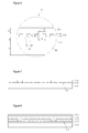
- FIG. 11 is a section view of a solar cell according to an embodiment of the present invention.
- a solar cell of the embodiment includes a substrate 100, a pattern layer 170, a back electrode 200, a light absorption layer 300, a buffer layer 400 and a front electrode 500.
- the pattern layer 170 includes an uneven pattern 150, curves having a quadrangular pyramid or sine wave shape may be periodically formed in the uneven pattern 150.
- the uneven pattern 150 includes grooves 110 and protrusions 120, the width of the grooves is 100 ⁇ 300nm, the width of the protrusions is 100 ⁇ 200nm, and the height of the grooves and protrusions may be 100-300nm.
- the grooves 110 and the protrusions 120 are formed by an uneven structure, so the grooves 120 have the shape protruded from the substrate 100.
- grooves 110 and the protrusions 120 allow a contact area to widen, it is possible to increase the combination between the substrate 100 and the back electrode formed hereafter.
- the substrate 100 is flexible, although the substrate 100 is curved, it is possible to prevent generation of the crack in the back electrode by the pattern layer 170.
- the back electrode is formed even in the inside of the grooves 110 of the uneven pattern 150, so it is possible to increase the combination force the substrate 100 and the back electrode.
- the pattern layer 170 may be formed by the material containing resin of single or mixture type such as epoxy, epoxy melanin, acrylic and urethane resin.
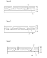
- FIGS. 1 to 11 are sectional views showing the method of fabricating the solar cell according to an embodiment of the present invention.
- the pattern layer 170 including the uneven pattern 150 is formed on the substrate 100.
- the substrate 100 uses glass and also uses ceramic substrate such as alumina, stainless steel, titanium substrate or polymer substrate and the like, as the material thereof.
- the glass substrate may use sodalime glass
- the polymer substrate may use PET(polyethylen terephthalate), and polyimide.
- the substrate 100 may be rigid or flexible.
- the uneven pattern 150 may form the uneven pattern in the resin layer.
- a method forming the pattern forms the resin layer on the substrate 100, and applies a molding process using a mold 230 while simultaneously applying UV hardening process.
- the resin layer may be formed by the material containing resin of single or mixture type such as epoxy, epoxy melanin, acrylic and urethane resin.
- the method forming the pattern is not limited thereto, after forming the resin layer on the substrate 100, it may be formed using laser light source.
- FIG. 3 and 4 in detail show 'A' region of FIG.1 , the uneven pattern 150, the uneven pattern 150 includes the grooves 110 and the protrusions 120, and the curve of the uneven pattern 150 having a square pillar shape is periodically formed.
- the grooves 110 and protrusions 120 are formed by an uneven structure, so the grooves 120 have the shape protruded from the substrate 100.
- grooves 110 and the protrusions 120 allows a contact area to widen, so it is possible to increase coupling force between the substrate 100 and the back electrode formed hereafter.
- the substrate 100 is flexible, although the substrate 100 is curved, tensile stress is transferred into the back electrode by the pattern layer 170, thereby to prevent the generation of the crack.
- the width f of the grooves 110 is 100 ⁇ 300nm
- the width g of the protrusions 120 is 100 ⁇ 200nm
- the height b of the grooves 110 and the height c of protrusions 120 may be 100-300nm.
- the uneven pattern 150 includes the grooves 110 and the protrusions 120, but is not limited thereto, and may be formed by the structure formed with the pattern capable of improving the coupling force with the back electrode to be formed later.
- the uneven pattern 150 having a square pillar shape may be formed longer in one direction.
- the uneven pattern 150 is not limited to the square pillar, as shown in FIG. 4 , the curve of the uneven pattern 160 having a curved sine wave shape may be periodically formed.
- the pattern layer 170 may be formed by the material containing resin of single or mixture type such as epoxy, epoxy melanin, acrylic and urethane resin.
- the coupling force between the pattern layer 170 and the substrate 100 is strong, the coupling force between the substrate 100 and the back electrode to be formed later may be also strengthened.
- the back electrode 201 is formed on the pattern layer 170.
- the back electrode 201 becomes a conductive layer.
- the back electrode layer 201 allows charges produced from the light absorption layer 300 of the solar cell to move, such that current may flow outside the solar cell.
- the back electrode layer 201 should be have high electrical conductivity and small specific resistance to perform above function.
- the back electrode layer 201 should be maintained to have high temperature stability when heat-treating under the atmosphere of sulfur(S) or selenium(Se) accompanied in forming CIGS compound.
- Such a back electrode 201 may be formed by any one of molybdenum (Mo), gold (Au), aluminum (Al), chromium (Cr), tungsten (W) and copper (Cu) Among them, particularly, the molybdenum (Mo) may allow the characteristic required for the back electrode layer 201 to generally satisfy.
- Mo molybdenum
- Au gold
- Al aluminum
- Cr chromium
- W tungsten
- Cu copper
- the molybdenum (Mo) may allow the characteristic required for the back electrode layer 201 to generally satisfy.
- the back electrode layer 201 may include at least two layers. In this case, each layer may be formed by same metal or metals different from each other.
- the back electrode 201 is also inserted into the inside of the grooves 110 of the uneven pattern 150 to increase the coupling force between the back electrode 201 and the substrate 100.
- the side in which the back electrode 201 contacts the pattern layer 170 may be formed to have a concave-convex corresponding to the uneven pattern of the pattern layer 170, and a top surface of the back electrode 201 may be formed to have the side parallel to the substrate 100.
- the substrate 100 is flexible, although the substrate 100 is curved by the difference in the thermal expansivity between the substrate and the back electrode, it is possible to prevent the generation of the crack between the substrate 100 and the back electrode, by the uneven pattern 150 formed on the substrate.
- the thickness of the substrate 100 is thicker than that of the uneven pattern 150 and the back electrode 201, and the thickness of the back electrode 201 is thicker than that of the uneven pattern 150.
- W has a value of 0.17 ⁇ 0.43
- X has a value of 0.03 ⁇ 0.15
- Y has a value of 0.04 ⁇ 0.12
- Z has a value of 1 ⁇ 2.
- a is a distance from the top surface of the uneven pattern 150, that is, the top surface of the protrusions 120 to the top surface of the back electrode pattern 201
- b is a height of the grooves 110
- c is a height of the grooves 120
- d is a thickness from the bottom surface of the grooves 110 to the substrate 100 in the pattern layer 170.
- e is a thickness of the substrate 100
- f is a width of the grooves 110
- g is a width of the protrusions 120.
- conditional expression (1) shows the relationship between the back electrode 201 and the pattern layer 170.
- the buffer layer that is, the d region of the pattern layer 170 become thicker, thereby to reduce the adhesion between the substrate 100 and the pattern 170.
- the difference in the thickness between the entire back electrode 201 and the pattern 170 is decreased, and therefore, d has not enough thickness in the pattern 170, such that the buffer function preventing the generation of the crack may be reduced.
- the conditional (2) means the percentage of the protrusions 120 or the grooves 11 in the entire thickness of the pattern layer 170.
- the height c of the protrusions 120 may be 0.03 ⁇ 0.15(X) times d, that is, the thickness from the bottom surface of the grooves 110 to the substrate 100 in the pattern layer 170.
- the height of the protrusions 120 that is, the value of c becomes larger, and therefore, it is hard to manufacture the uneven pattern 150. Further, it is not deposited up to the bottom surface of the grooves 110 when depositing the back electrode 201, thereby to reduce the buffer function preventing the generation of the crack.
- conditional expression (3) shows the relationship between the substrate 100, and the region of d, that is, the thickness from the bottom surface of the grooves 110 to the substrate 100 in the pattern layer 170.
- the value of d that is, the thickness of the pattern layer 170 from the bottom surface of the grooves 110 to the substrate 100 may become 0.04 ⁇ 0.12(Y) times the substrate 100.
- the thickness of the substrate 100 is relatively decreased, such that bending phenomenon easily occurs in the substrate, thereby to easily produce the crack.
- conditional expression (4) shows the relationship about the percentage between the widths f of the grooves 110 and the widths g of the protrusions 120.
- the width f of the grooves 110 may be 1 ⁇ 2 (Z) times the width g of the protrusions 120.
- the period h of the uneven pattern 150 may be formed regularly or irregularly, and may be formed by the period of 200-500nm.
- the back electrode 201 is harder than the substrate 100 and the uneven pattern 150, and the hardness of the substrate 100 is harder than or equal to that of the uneven pattern 150.
- the back electrode pattern 200 is formed by applying a patterning process to the back electrode 201.
- the back electrode pattern 200 may be formed by applying a photolithography process to the back electrode 201.
- the back electrode pattern 200 may be arranged in a stripe type or a matrix type to correspond to each cell.
- the back electrode pattern 200 is not limited to above type, and may be formed in various types.
- the portion of the uneven pattern 150 formed on the substrate 100 may be exposed through the back electrode pattern 200.
- the light absorption layer 300 and the buffer layer 400 are formed on the back electrode pattern 200.
- the light absorption layer 300 includes p-type semiconductor compound.
- the light absorption layer 300 includes group - - -base compound.
- the light absorption layer 300 may has copper-indium-gallium-selenide-base(Cu(In,Ga)Se2;CIGS-base) or copper-gallium-selenide-base crystal structure.
- a CIG-base metal precursor film is formed on the back electrode pattern 200 by using copper target, indium target and gallium target.
- the metal precursor film reacts with selenium by a selenization process to form a CIG-base light absorption layer 300.
- alkali ingredients contained in the substrate 100 are diffused into the metal precursor film and the light absorption layer 300 through the back electrode pattern 200.
- the alkali component improves a grain size of the light absorption layer 300 to improve crystallizability.
- the light absorption layer 300 may be formed by copper, indium, gallium and selenium(Cu, In, Ga and Se) by coevaporation
- the light absorption layer 300 receives light incident from the outside, and converts the received light into electrical energy.
- the light absorption layer 300 produces light electromotive force generated by photoelectric effect.
- the portion of the light absorption layer 300 contacting the substrate 100 is also formed on the uneven pattern 150.
- the portion of the light absorption layer 300 is also coupled with the grooves 110 and the protrusions 120 of the uneven pattern 150, such that coupling force of the light absorption layer 300 and the substrate 100 may be increased.
- the buffer layer 400 may be formed by at least one layer, may be formed by any one of cadmium sulfide(CdS), ITO, ZnO and i-2nO or laminating of them on the substrate 100 formed with the light absorption layer 300, and may obtain low resistance by doping indium(In), gallium(Ga) and aluminum(Al).
- the buffer layer 400 is an n-type semiconductor layer, and the light absorption layer 300 is a p-type semiconductor layer. As a result, the light absorption layer 300 and the buffer layer 400 form pn-junction.
- the buffer layer 400 is arranged between the light absorption layer 300, and the front electrode to be formed later.
- the light absorption layer 300 and the front electrode have large difference in a lattice constant and band gap energy, to form good junction, a buffer layer to be positioned in the middle of the two materials is necessary due to the difference in the band gap.
- a buffer layer is formed on the light absorption layer 300, is not limited thereto, and the buffer layer 400 may be formed by a plurality of layers.
- contact patterns are formed through the light absorption layer 300 and the buffer layer 400.
- the contact patterns 310 may be formed by applying a mechanical method or a process using laser, and the portion of the back electrode pattern 200 is exposed.
- the front electrode 500 and a connecting interconnection 700 are formed by laminating transparent conductive material on the buffer layer 400.
- the transparent conductive material is also inserted into the inside of the contact pattern 310 to form the connecting interconnection 700.
- the back electrode pattern 200 and the front electrode 500 are electrically connected to each other by the connecting interconnection 700.
- the front electrode 500 is formed by zinc oxide doped with the aluminum by applying the sputtering process on the substrate 100.
- the front electrode 500 which is a window layer forming the pn-junction with the light absorption layer 300, functions as the transparent electrode of the front of the solar cell, and therefore, is formed by the zinc oxide (ZnO) having high light transmittance and good electrical conductivity.
- ZnO zinc oxide
- the electrode having a low resistance may be formed by doping the aluminum to the zinc oxide
- the front electrode 500 that is, the zinc oxide thin film may be formed by a deposition method using ZnO target by RF sputtering method, reactive sputtering using Zn target, and metal organic chemical vapor deposition.
- separate patterns 320 are formed through the light absorption layer 300, the buffer layer 400, and the front electrode 500.
- the separate patterns 320 may be formed by applying a mechanical method or a process using laser, and the portion of the back electrode pattern 200 is exposed.
- the buffer layer 400, and the front electrode 500 may be divided by the separate pattern 320, and each of cells C1, C2 may be separated to each other by the separate pattern 320.
- the light absorption layer 300, the buffer layer 400, and the front electrode 500 may be arranged in a stripe type or a matrix type by the separate pattern 320.
- the separate pattern 320 is not limited to above type, and may be formed in various types.
- the cells C1, C2 including the back electrode pattern 200, the light absorption layer 300, the buffer layer 400, and the front electrode 500 are formed by the separate pattern 320.
- each of the cells C1, C2 are connected to each other by the connecting interconnection 700.
- the back electrode pattern 200 of the second cell C2 and the front electrode 500 of the first cell C1 contacting the second cell C2 are connected to each other by the connecting interconnection 700.
- the solar cell and method fabricating the same according to the embodiments described above may form the uneven pattern having a nano size on the substrate, thereby to increase the coupling force with the back electrode formed on the substrate.
- the crack does not occur between the substrate and the back electrode.
- the back electrode is formed even in the inside of the grooves of the uneven structure pattern to increase the coupling force between the substrate and the back electrode.
- the light absorption layer in which the portion thereof contacts the substrate, also contacts the uneven structure pattern to increase the coupling force between the light absorption layer and the substrate.
- the solar cell and method fabricating the same according to the embodiment may form the uneven pattern having a nano size on the substrate, thereby to increase the coupling force with the back electrode formed on the substrate.
- the crack does not occur between the substrate and the back electrode.
- the back electrode is formed even in the inside of the grooves of the uneven structure pattern to increase the coupling force between the substrate and the back electrode.
- the light absorption layer in which the portion thereof contacts the substrate, also contacts the uneven structure pattern to increase the coupling force between the light absorption layer and the substrate.
Landscapes
- Photovoltaic Devices (AREA)
- Engineering & Computer Science (AREA)
- Life Sciences & Earth Sciences (AREA)
- Sustainable Energy (AREA)
- Manufacturing & Machinery (AREA)
- Physics & Mathematics (AREA)
- Electromagnetism (AREA)
Applications Claiming Priority (2)
| Application Number | Priority Date | Filing Date | Title |
|---|---|---|---|
| KR1020090103076A KR101091405B1 (ko) | 2009-10-28 | 2009-10-28 | 태양전지 및 이의 제조방법 |
| PCT/KR2010/007493 WO2011053025A2 (ko) | 2009-10-28 | 2010-10-28 | 태양전지 및 이의 제조방법 |
Publications (2)
| Publication Number | Publication Date |
|---|---|
| EP2434550A2 true EP2434550A2 (de) | 2012-03-28 |
| EP2434550A4 EP2434550A4 (de) | 2013-11-20 |
Family
ID=43922852
Family Applications (1)
| Application Number | Title | Priority Date | Filing Date |
|---|---|---|---|
| EP10827109.9A Withdrawn EP2434550A4 (de) | 2009-10-28 | 2010-10-28 | Solarzelle und herstellungsverfahren dafür |
Country Status (6)
| Country | Link |
|---|---|
| US (1) | US8987585B2 (de) |
| EP (1) | EP2434550A4 (de) |
| JP (1) | JP5663030B2 (de) |
| KR (1) | KR101091405B1 (de) |
| CN (1) | CN102598299A (de) |
| WO (1) | WO2011053025A2 (de) |
Families Citing this family (9)
| Publication number | Priority date | Publication date | Assignee | Title |
|---|---|---|---|---|
| KR101186560B1 (ko) * | 2011-07-07 | 2012-10-08 | 포항공과대학교 산학협력단 | 태양전지용 기판 및 이의 제조방법 |
| KR101281005B1 (ko) * | 2011-07-20 | 2013-07-08 | (주)에스티아이 | 박막형 태양전지 |
| FR2979752B1 (fr) * | 2011-09-02 | 2016-03-11 | Commissariat Energie Atomique | Dispositif photovoltaique non plan |
| KR101272998B1 (ko) * | 2011-10-13 | 2013-06-10 | 엘지이노텍 주식회사 | 태양전지 및 이를 이용한 태양전지 모듈 |
| CN103000709B (zh) * | 2012-11-26 | 2017-02-08 | 北京大学深圳研究生院 | 背电极、背电极吸收层复合结构及太阳能电池 |
| JP6085879B2 (ja) * | 2012-12-17 | 2017-03-01 | ローム株式会社 | 光電変換装置の製造方法 |
| KR20150039536A (ko) * | 2013-10-02 | 2015-04-10 | 엘지이노텍 주식회사 | 태양전지 |
| KR102514594B1 (ko) | 2015-08-13 | 2023-03-27 | 삼성전자주식회사 | 유연한 전기화학소자용 외장 포장재 및 이를 포함하는 전기화학소자 |
| CN114759101B (zh) * | 2020-12-29 | 2023-08-01 | 隆基绿能科技股份有限公司 | 一种热载流子太阳能电池及光伏组件 |
Family Cites Families (16)
| Publication number | Priority date | Publication date | Assignee | Title |
|---|---|---|---|---|
| JP2994810B2 (ja) | 1991-09-13 | 1999-12-27 | 三洋電機株式会社 | 光起電力装置及びその製造方法 |
| JPH05308148A (ja) * | 1992-03-05 | 1993-11-19 | Tdk Corp | 太陽電池 |
| EP0911884B1 (de) * | 1997-10-27 | 2005-02-09 | Sharp Kabushiki Kaisha | Photoelektrische Wandler und sein Herstellungsverfahren |
| JP2000208800A (ja) * | 1998-11-13 | 2000-07-28 | Fuji Xerox Co Ltd | 太陽電池及びそれを用いた自己電力供給型表示素子、並びに太陽電池の製造方法 |
| JP2001345460A (ja) * | 2000-03-29 | 2001-12-14 | Sanyo Electric Co Ltd | 太陽電池装置 |
| JP2003298086A (ja) | 2002-03-29 | 2003-10-17 | Tdk Corp | 太陽電池およびその製造方法 |
| JP2003298084A (ja) * | 2002-03-29 | 2003-10-17 | Tdk Corp | 太陽電池およびその製造方法 |
| JP4215608B2 (ja) * | 2003-09-26 | 2009-01-28 | 三洋電機株式会社 | 光起電力装置 |
| JP2005150242A (ja) * | 2003-11-12 | 2005-06-09 | Japan Gore Tex Inc | 太陽電池基板およびその製造方法、並びに太陽電池 |
| JP2007201304A (ja) | 2006-01-30 | 2007-08-09 | Honda Motor Co Ltd | 太陽電池およびその製造方法 |
| US8716594B2 (en) * | 2006-09-26 | 2014-05-06 | Banpil Photonics, Inc. | High efficiency photovoltaic cells with self concentrating effect |
| JP5048380B2 (ja) | 2007-04-09 | 2012-10-17 | 信越化学工業株式会社 | 単結晶シリコン太陽電池の製造方法 |
| KR20080107181A (ko) * | 2007-06-05 | 2008-12-10 | 엘지전자 주식회사 | 고효율 태양전지 |
| JP4304638B2 (ja) | 2007-07-13 | 2009-07-29 | オムロン株式会社 | Cis系太陽電池及びその製造方法 |
| KR101494153B1 (ko) | 2007-12-21 | 2015-02-23 | 주성엔지니어링(주) | 박막형 태양전지 및 그 제조방법 |
| WO2009082137A2 (en) * | 2007-12-21 | 2009-07-02 | Jusung Engineering Co., Ltd. | Thin film type solar cell and method for manufacturing the same |
-
2009
- 2009-10-28 KR KR1020090103076A patent/KR101091405B1/ko not_active Expired - Fee Related
-
2010
- 2010-10-28 US US13/379,557 patent/US8987585B2/en not_active Expired - Fee Related
- 2010-10-28 EP EP10827109.9A patent/EP2434550A4/de not_active Withdrawn
- 2010-10-28 CN CN2010800492881A patent/CN102598299A/zh active Pending
- 2010-10-28 JP JP2012536683A patent/JP5663030B2/ja not_active Expired - Fee Related
- 2010-10-28 WO PCT/KR2010/007493 patent/WO2011053025A2/ko not_active Ceased
Also Published As
| Publication number | Publication date |
|---|---|
| CN102598299A (zh) | 2012-07-18 |
| EP2434550A4 (de) | 2013-11-20 |
| WO2011053025A2 (ko) | 2011-05-05 |
| KR20110046195A (ko) | 2011-05-04 |
| JP2013509705A (ja) | 2013-03-14 |
| US20120097242A1 (en) | 2012-04-26 |
| WO2011053025A3 (ko) | 2011-09-22 |
| KR101091405B1 (ko) | 2011-12-07 |
| US8987585B2 (en) | 2015-03-24 |
| JP5663030B2 (ja) | 2015-02-04 |
Similar Documents
| Publication | Publication Date | Title |
|---|---|---|
| EP2434550A2 (de) | Solarzelle und herstellungsverfahren dafür | |
| EP2410575B1 (de) | Solarbatterie und herstellungsverfahren dafür | |
| US20120186624A1 (en) | Solar Cell and Manufacturing Method Thereof | |
| US20120180869A1 (en) | Solar power generation apparatus and manufacturing method thereof | |
| US20120174977A1 (en) | Solar Power Generation Apparatus and Manufacturing Method Thereof | |
| KR101081292B1 (ko) | 태양전지 및 이의 제조방법 | |
| US9748424B2 (en) | Solar cell and preparing method of the same | |
| EP2533298A1 (de) | Photovoltaikvorrichtung und herstellungsverfahren dafür | |
| US20140326290A1 (en) | Solar cell and solar cell module | |
| KR101091357B1 (ko) | 태양전지 및 이의 제조방법 | |
| KR101072106B1 (ko) | 태양전지 및 이의 제조방법 | |
| US10020414B2 (en) | Solar cell and manufacturing method therefor | |
| US20130220398A1 (en) | Solar cell and method for manufacturing the same | |
| JP5947315B2 (ja) | 太陽電池 | |
| US9178084B2 (en) | Solar cell and method for manufacturing the same | |
| US9941427B2 (en) | Solar cell and method of fabricating the same | |
| KR101306525B1 (ko) | 태양전지 모듈 및 이의 제조방법 | |
| EP2695201B1 (de) | Solarzelle | |
| KR20140015936A (ko) | 태양전지 및 이의 제조 방법 | |
| KR101417213B1 (ko) | 태양전지 모듈 및 이의 제조방법 | |
| KR101034146B1 (ko) | 태양전지 및 이의 제조방법 | |
| US20140182653A1 (en) | Solar cell and solar cell module using the same | |
| US20130125981A1 (en) | Solar cell and manufacturing method thereof | |
| KR101934434B1 (ko) | 태양전지 및 이의 제조 방법 | |
| KR101091499B1 (ko) | 팁, 태양전지 및 팁을 이용한 태양전지의 제조방법 |
Legal Events
| Date | Code | Title | Description |
|---|---|---|---|
| PUAI | Public reference made under article 153(3) epc to a published international application that has entered the european phase |
Free format text: ORIGINAL CODE: 0009012 |
|
| 17P | Request for examination filed |
Effective date: 20111221 |
|
| AK | Designated contracting states |
Kind code of ref document: A2 Designated state(s): AL AT BE BG CH CY CZ DE DK EE ES FI FR GB GR HR HU IE IS IT LI LT LU LV MC MK MT NL NO PL PT RO RS SE SI SK SM TR |
|
| DAX | Request for extension of the european patent (deleted) | ||
| A4 | Supplementary search report drawn up and despatched |
Effective date: 20131021 |
|
| RIC1 | Information provided on ipc code assigned before grant |
Ipc: H01L 31/0749 20120101ALI20131015BHEP Ipc: H01L 31/0392 20060101ALI20131015BHEP Ipc: H01L 27/142 20060101AFI20131015BHEP |
|
| 17Q | First examination report despatched |
Effective date: 20131106 |
|
| STAA | Information on the status of an ep patent application or granted ep patent |
Free format text: STATUS: THE APPLICATION HAS BEEN WITHDRAWN |
|
| 18W | Application withdrawn |
Effective date: 20140311 |