EP2428512A2 - Fluorenverbindung, lichtemittierendes Element, lichtemittierende Vorrichtung, elektronische Vorrichtung und Beleuchtungsvorrichtung. - Google Patents
Fluorenverbindung, lichtemittierendes Element, lichtemittierende Vorrichtung, elektronische Vorrichtung und Beleuchtungsvorrichtung. Download PDFInfo
- Publication number
- EP2428512A2 EP2428512A2 EP11179794A EP11179794A EP2428512A2 EP 2428512 A2 EP2428512 A2 EP 2428512A2 EP 11179794 A EP11179794 A EP 11179794A EP 11179794 A EP11179794 A EP 11179794A EP 2428512 A2 EP2428512 A2 EP 2428512A2
- Authority
- EP
- European Patent Office
- Prior art keywords
- light
- emitting element
- emitting
- carbon atoms
- group
- Prior art date
- Legal status (The legal status is an assumption and is not a legal conclusion. Google has not performed a legal analysis and makes no representation as to the accuracy of the status listed.)
- Granted
Links
- 0 C1C2C(C3)C3*CC12 Chemical compound C1C2C(C3)C3*CC12 0.000 description 3
- BHTLJXDKHJWTBJ-UHFFFAOYSA-N C(C1)C=CC(c2c3cccc2)=C1C3(c1cc(-c2cccc3c2[o]c2ccccc32)ccc1)c1cc(-c2c3[o]c(cccc4)c4c3ccc2)ccc1 Chemical compound C(C1)C=CC(c2c3cccc2)=C1C3(c1cc(-c2cccc3c2[o]c2ccccc32)ccc1)c1cc(-c2c3[o]c(cccc4)c4c3ccc2)ccc1 BHTLJXDKHJWTBJ-UHFFFAOYSA-N 0.000 description 1
- MDNBCWSFAXIVNL-UHFFFAOYSA-N C(C1c2ccccc2)C=Cc2c1[s]c1c2cccc1-c1cccc(C2(c3ccccc3-c3c2cccc3)c2cccc(-c3c4[s]c(c(-c5ccccc5)ccc5)c5c4ccc3)c2)c1 Chemical compound C(C1c2ccccc2)C=Cc2c1[s]c1c2cccc1-c1cccc(C2(c3ccccc3-c3c2cccc3)c2cccc(-c3c4[s]c(c(-c5ccccc5)ccc5)c5c4ccc3)c2)c1 MDNBCWSFAXIVNL-UHFFFAOYSA-N 0.000 description 1
- BIOCIFZZLUFDTP-UHFFFAOYSA-N C1C=C(C2(c3ccccc3-c3c2cccc3)c(cc2)ccc2-c2c3[s]c(c(-c4ccccc4)ccc4)c4c3ccc2)C=CC1C(CC=C1)c2c1c(cccc1-c3ccccc3)c1[s]2 Chemical compound C1C=C(C2(c3ccccc3-c3c2cccc3)c(cc2)ccc2-c2c3[s]c(c(-c4ccccc4)ccc4)c4c3ccc2)C=CC1C(CC=C1)c2c1c(cccc1-c3ccccc3)c1[s]2 BIOCIFZZLUFDTP-UHFFFAOYSA-N 0.000 description 1
- UPEFLZIQOBJLAZ-UHFFFAOYSA-N c(cc12)ccc1-c1ccccc1C2(c(cc1)ccc1-c1c2[o]c(cccc3)c3c2ccc1)c(cc1)ccc1-c1c2[o]c3ccccc3c2ccc1 Chemical compound c(cc12)ccc1-c1ccccc1C2(c(cc1)ccc1-c1c2[o]c(cccc3)c3c2ccc1)c(cc1)ccc1-c1c2[o]c3ccccc3c2ccc1 UPEFLZIQOBJLAZ-UHFFFAOYSA-N 0.000 description 1
Images


Classifications
-
- C—CHEMISTRY; METALLURGY
- C07—ORGANIC CHEMISTRY
- C07C—ACYCLIC OR CARBOCYCLIC COMPOUNDS
- C07C25/00—Compounds containing at least one halogen atom bound to a six-membered aromatic ring
- C07C25/18—Polycyclic aromatic halogenated hydrocarbons
- C07C25/22—Polycyclic aromatic halogenated hydrocarbons with condensed rings
-
- H—ELECTRICITY
- H10—SEMICONDUCTOR DEVICES; ELECTRIC SOLID-STATE DEVICES NOT OTHERWISE PROVIDED FOR
- H10K—ORGANIC ELECTRIC SOLID-STATE DEVICES
- H10K85/00—Organic materials used in the body or electrodes of devices covered by this subclass
- H10K85/60—Organic compounds having low molecular weight
- H10K85/649—Aromatic compounds comprising a hetero atom
- H10K85/657—Polycyclic condensed heteroaromatic hydrocarbons
- H10K85/6574—Polycyclic condensed heteroaromatic hydrocarbons comprising only oxygen in the heteroaromatic polycondensed ring system, e.g. cumarine dyes
-
- C—CHEMISTRY; METALLURGY
- C07—ORGANIC CHEMISTRY
- C07C—ACYCLIC OR CARBOCYCLIC COMPOUNDS
- C07C25/00—Compounds containing at least one halogen atom bound to a six-membered aromatic ring
- C07C25/02—Monocyclic aromatic halogenated hydrocarbons
-
- C—CHEMISTRY; METALLURGY
- C07—ORGANIC CHEMISTRY
- C07C—ACYCLIC OR CARBOCYCLIC COMPOUNDS
- C07C31/00—Saturated compounds having hydroxy or O-metal groups bound to acyclic carbon atoms
- C07C31/34—Halogenated alcohols
- C07C31/36—Halogenated alcohols the halogen not being fluorine
-
- C—CHEMISTRY; METALLURGY
- C07—ORGANIC CHEMISTRY
- C07C—ACYCLIC OR CARBOCYCLIC COMPOUNDS
- C07C33/00—Unsaturated compounds having hydroxy or O-metal groups bound to acyclic carbon atoms
- C07C33/40—Halogenated unsaturated alcohols
- C07C33/46—Halogenated unsaturated alcohols containing only six-membered aromatic rings as cyclic parts
-
- C—CHEMISTRY; METALLURGY
- C07—ORGANIC CHEMISTRY
- C07C—ACYCLIC OR CARBOCYCLIC COMPOUNDS
- C07C33/00—Unsaturated compounds having hydroxy or O-metal groups bound to acyclic carbon atoms
- C07C33/40—Halogenated unsaturated alcohols
- C07C33/50—Halogenated unsaturated alcohols containing six-membered aromatic rings and other rings
-
- C—CHEMISTRY; METALLURGY
- C07—ORGANIC CHEMISTRY
- C07C—ACYCLIC OR CARBOCYCLIC COMPOUNDS
- C07C49/00—Ketones; Ketenes; Dimeric ketenes; Ketonic chelates
- C07C49/04—Saturated compounds containing keto groups bound to acyclic carbon atoms
- C07C49/16—Saturated compounds containing keto groups bound to acyclic carbon atoms containing halogen
- C07C49/163—Saturated compounds containing keto groups bound to acyclic carbon atoms containing halogen containing rings
-
- C—CHEMISTRY; METALLURGY
- C07—ORGANIC CHEMISTRY
- C07C—ACYCLIC OR CARBOCYCLIC COMPOUNDS
- C07C49/00—Ketones; Ketenes; Dimeric ketenes; Ketonic chelates
- C07C49/29—Saturated compounds containing keto groups bound to rings
- C07C49/327—Saturated compounds containing keto groups bound to rings containing halogen
- C07C49/333—Saturated compounds containing keto groups bound to rings containing halogen polycyclic
-
- C—CHEMISTRY; METALLURGY
- C07—ORGANIC CHEMISTRY
- C07C—ACYCLIC OR CARBOCYCLIC COMPOUNDS
- C07C49/00—Ketones; Ketenes; Dimeric ketenes; Ketonic chelates
- C07C49/76—Ketones containing a keto group bound to a six-membered aromatic ring
- C07C49/80—Ketones containing a keto group bound to a six-membered aromatic ring containing halogen
- C07C49/813—Ketones containing a keto group bound to a six-membered aromatic ring containing halogen polycyclic
-
- C—CHEMISTRY; METALLURGY
- C07—ORGANIC CHEMISTRY
- C07D—HETEROCYCLIC COMPOUNDS
- C07D307/00—Heterocyclic compounds containing five-membered rings having one oxygen atom as the only ring hetero atom
- C07D307/77—Heterocyclic compounds containing five-membered rings having one oxygen atom as the only ring hetero atom ortho- or peri-condensed with carbocyclic rings or ring systems
- C07D307/91—Dibenzofurans; Hydrogenated dibenzofurans
-
- C—CHEMISTRY; METALLURGY
- C07—ORGANIC CHEMISTRY
- C07D—HETEROCYCLIC COMPOUNDS
- C07D333/00—Heterocyclic compounds containing five-membered rings having one sulfur atom as the only ring hetero atom
- C07D333/50—Heterocyclic compounds containing five-membered rings having one sulfur atom as the only ring hetero atom condensed with carbocyclic rings or ring systems
- C07D333/76—Dibenzothiophenes
-
- C—CHEMISTRY; METALLURGY
- C07—ORGANIC CHEMISTRY
- C07D—HETEROCYCLIC COMPOUNDS
- C07D409/00—Heterocyclic compounds containing two or more hetero rings, at least one ring having sulfur atoms as the only ring hetero atoms
- C07D409/02—Heterocyclic compounds containing two or more hetero rings, at least one ring having sulfur atoms as the only ring hetero atoms containing two hetero rings
- C07D409/10—Heterocyclic compounds containing two or more hetero rings, at least one ring having sulfur atoms as the only ring hetero atoms containing two hetero rings linked by a carbon chain containing aromatic rings
-
- C—CHEMISTRY; METALLURGY
- C09—DYES; PAINTS; POLISHES; NATURAL RESINS; ADHESIVES; COMPOSITIONS NOT OTHERWISE PROVIDED FOR; APPLICATIONS OF MATERIALS NOT OTHERWISE PROVIDED FOR
- C09K—MATERIALS FOR MISCELLANEOUS APPLICATIONS, NOT PROVIDED FOR ELSEWHERE
- C09K11/00—Luminescent, e.g. electroluminescent, chemiluminescent materials
- C09K11/06—Luminescent, e.g. electroluminescent, chemiluminescent materials containing organic luminescent materials
-
- H—ELECTRICITY
- H05—ELECTRIC TECHNIQUES NOT OTHERWISE PROVIDED FOR
- H05B—ELECTRIC HEATING; ELECTRIC LIGHT SOURCES NOT OTHERWISE PROVIDED FOR; CIRCUIT ARRANGEMENTS FOR ELECTRIC LIGHT SOURCES, IN GENERAL
- H05B33/00—Electroluminescent light sources
- H05B33/10—Apparatus or processes specially adapted to the manufacture of electroluminescent light sources
-
- H—ELECTRICITY
- H10—SEMICONDUCTOR DEVICES; ELECTRIC SOLID-STATE DEVICES NOT OTHERWISE PROVIDED FOR
- H10K—ORGANIC ELECTRIC SOLID-STATE DEVICES
- H10K50/00—Organic light-emitting devices
- H10K50/10—OLEDs or polymer light-emitting diodes [PLED]
- H10K50/14—Carrier transporting layers
- H10K50/15—Hole transporting layers
-
- H—ELECTRICITY
- H10—SEMICONDUCTOR DEVICES; ELECTRIC SOLID-STATE DEVICES NOT OTHERWISE PROVIDED FOR
- H10K—ORGANIC ELECTRIC SOLID-STATE DEVICES
- H10K85/00—Organic materials used in the body or electrodes of devices covered by this subclass
- H10K85/30—Coordination compounds
- H10K85/321—Metal complexes comprising a group IIIA element, e.g. Tris (8-hydroxyquinoline) gallium [Gaq3]
- H10K85/324—Metal complexes comprising a group IIIA element, e.g. Tris (8-hydroxyquinoline) gallium [Gaq3] comprising aluminium, e.g. Alq3
-
- H—ELECTRICITY
- H10—SEMICONDUCTOR DEVICES; ELECTRIC SOLID-STATE DEVICES NOT OTHERWISE PROVIDED FOR
- H10K—ORGANIC ELECTRIC SOLID-STATE DEVICES
- H10K85/00—Organic materials used in the body or electrodes of devices covered by this subclass
- H10K85/30—Coordination compounds
- H10K85/341—Transition metal complexes, e.g. Ru(II)polypyridine complexes
- H10K85/342—Transition metal complexes, e.g. Ru(II)polypyridine complexes comprising iridium
-
- H—ELECTRICITY
- H10—SEMICONDUCTOR DEVICES; ELECTRIC SOLID-STATE DEVICES NOT OTHERWISE PROVIDED FOR
- H10K—ORGANIC ELECTRIC SOLID-STATE DEVICES
- H10K85/00—Organic materials used in the body or electrodes of devices covered by this subclass
- H10K85/60—Organic compounds having low molecular weight
- H10K85/615—Polycyclic condensed aromatic hydrocarbons, e.g. anthracene
- H10K85/622—Polycyclic condensed aromatic hydrocarbons, e.g. anthracene containing four rings, e.g. pyrene
-
- H—ELECTRICITY
- H10—SEMICONDUCTOR DEVICES; ELECTRIC SOLID-STATE DEVICES NOT OTHERWISE PROVIDED FOR
- H10K—ORGANIC ELECTRIC SOLID-STATE DEVICES
- H10K85/00—Organic materials used in the body or electrodes of devices covered by this subclass
- H10K85/60—Organic compounds having low molecular weight
- H10K85/615—Polycyclic condensed aromatic hydrocarbons, e.g. anthracene
- H10K85/626—Polycyclic condensed aromatic hydrocarbons, e.g. anthracene containing more than one polycyclic condensed aromatic rings, e.g. bis-anthracene
-
- H—ELECTRICITY
- H10—SEMICONDUCTOR DEVICES; ELECTRIC SOLID-STATE DEVICES NOT OTHERWISE PROVIDED FOR
- H10K—ORGANIC ELECTRIC SOLID-STATE DEVICES
- H10K85/00—Organic materials used in the body or electrodes of devices covered by this subclass
- H10K85/60—Organic compounds having low molecular weight
- H10K85/631—Amine compounds having at least two aryl rest on at least one amine-nitrogen atom, e.g. triphenylamine
- H10K85/633—Amine compounds having at least two aryl rest on at least one amine-nitrogen atom, e.g. triphenylamine comprising polycyclic condensed aromatic hydrocarbons as substituents on the nitrogen atom
-
- H—ELECTRICITY
- H10—SEMICONDUCTOR DEVICES; ELECTRIC SOLID-STATE DEVICES NOT OTHERWISE PROVIDED FOR
- H10K—ORGANIC ELECTRIC SOLID-STATE DEVICES
- H10K85/00—Organic materials used in the body or electrodes of devices covered by this subclass
- H10K85/60—Organic compounds having low molecular weight
- H10K85/649—Aromatic compounds comprising a hetero atom
- H10K85/657—Polycyclic condensed heteroaromatic hydrocarbons
- H10K85/6572—Polycyclic condensed heteroaromatic hydrocarbons comprising only nitrogen in the heteroaromatic polycondensed ring system, e.g. phenanthroline or carbazole
-
- H—ELECTRICITY
- H10—SEMICONDUCTOR DEVICES; ELECTRIC SOLID-STATE DEVICES NOT OTHERWISE PROVIDED FOR
- H10K—ORGANIC ELECTRIC SOLID-STATE DEVICES
- H10K85/00—Organic materials used in the body or electrodes of devices covered by this subclass
- H10K85/60—Organic compounds having low molecular weight
- H10K85/649—Aromatic compounds comprising a hetero atom
- H10K85/657—Polycyclic condensed heteroaromatic hydrocarbons
- H10K85/6576—Polycyclic condensed heteroaromatic hydrocarbons comprising only sulfur in the heteroaromatic polycondensed ring system, e.g. benzothiophene
-
- C—CHEMISTRY; METALLURGY
- C07—ORGANIC CHEMISTRY
- C07C—ACYCLIC OR CARBOCYCLIC COMPOUNDS
- C07C2603/00—Systems containing at least three condensed rings
- C07C2603/02—Ortho- or ortho- and peri-condensed systems
- C07C2603/04—Ortho- or ortho- and peri-condensed systems containing three rings
- C07C2603/06—Ortho- or ortho- and peri-condensed systems containing three rings containing at least one ring with less than six ring members
- C07C2603/10—Ortho- or ortho- and peri-condensed systems containing three rings containing at least one ring with less than six ring members containing five-membered rings
- C07C2603/12—Ortho- or ortho- and peri-condensed systems containing three rings containing at least one ring with less than six ring members containing five-membered rings only one five-membered ring
- C07C2603/18—Fluorenes; Hydrogenated fluorenes
-
- C—CHEMISTRY; METALLURGY
- C07—ORGANIC CHEMISTRY
- C07C—ACYCLIC OR CARBOCYCLIC COMPOUNDS
- C07C2603/00—Systems containing at least three condensed rings
- C07C2603/02—Ortho- or ortho- and peri-condensed systems
- C07C2603/04—Ortho- or ortho- and peri-condensed systems containing three rings
- C07C2603/22—Ortho- or ortho- and peri-condensed systems containing three rings containing only six-membered rings
- C07C2603/24—Anthracenes; Hydrogenated anthracenes
-
- C—CHEMISTRY; METALLURGY
- C07—ORGANIC CHEMISTRY
- C07C—ACYCLIC OR CARBOCYCLIC COMPOUNDS
- C07C2603/00—Systems containing at least three condensed rings
- C07C2603/02—Ortho- or ortho- and peri-condensed systems
- C07C2603/40—Ortho- or ortho- and peri-condensed systems containing four condensed rings
- C07C2603/42—Ortho- or ortho- and peri-condensed systems containing four condensed rings containing only six-membered rings
- C07C2603/50—Pyrenes; Hydrogenated pyrenes
-
- C—CHEMISTRY; METALLURGY
- C09—DYES; PAINTS; POLISHES; NATURAL RESINS; ADHESIVES; COMPOSITIONS NOT OTHERWISE PROVIDED FOR; APPLICATIONS OF MATERIALS NOT OTHERWISE PROVIDED FOR
- C09K—MATERIALS FOR MISCELLANEOUS APPLICATIONS, NOT PROVIDED FOR ELSEWHERE
- C09K2211/00—Chemical nature of organic luminescent or tenebrescent compounds
- C09K2211/10—Non-macromolecular compounds
- C09K2211/1003—Carbocyclic compounds
- C09K2211/1007—Non-condensed systems
-
- C—CHEMISTRY; METALLURGY
- C09—DYES; PAINTS; POLISHES; NATURAL RESINS; ADHESIVES; COMPOSITIONS NOT OTHERWISE PROVIDED FOR; APPLICATIONS OF MATERIALS NOT OTHERWISE PROVIDED FOR
- C09K—MATERIALS FOR MISCELLANEOUS APPLICATIONS, NOT PROVIDED FOR ELSEWHERE
- C09K2211/00—Chemical nature of organic luminescent or tenebrescent compounds
- C09K2211/10—Non-macromolecular compounds
- C09K2211/1003—Carbocyclic compounds
- C09K2211/1011—Condensed systems
-
- C—CHEMISTRY; METALLURGY
- C09—DYES; PAINTS; POLISHES; NATURAL RESINS; ADHESIVES; COMPOSITIONS NOT OTHERWISE PROVIDED FOR; APPLICATIONS OF MATERIALS NOT OTHERWISE PROVIDED FOR
- C09K—MATERIALS FOR MISCELLANEOUS APPLICATIONS, NOT PROVIDED FOR ELSEWHERE
- C09K2211/00—Chemical nature of organic luminescent or tenebrescent compounds
- C09K2211/10—Non-macromolecular compounds
- C09K2211/1018—Heterocyclic compounds
- C09K2211/1025—Heterocyclic compounds characterised by ligands
- C09K2211/1088—Heterocyclic compounds characterised by ligands containing oxygen as the only heteroatom
-
- C—CHEMISTRY; METALLURGY
- C09—DYES; PAINTS; POLISHES; NATURAL RESINS; ADHESIVES; COMPOSITIONS NOT OTHERWISE PROVIDED FOR; APPLICATIONS OF MATERIALS NOT OTHERWISE PROVIDED FOR
- C09K—MATERIALS FOR MISCELLANEOUS APPLICATIONS, NOT PROVIDED FOR ELSEWHERE
- C09K2211/00—Chemical nature of organic luminescent or tenebrescent compounds
- C09K2211/10—Non-macromolecular compounds
- C09K2211/1018—Heterocyclic compounds
- C09K2211/1025—Heterocyclic compounds characterised by ligands
- C09K2211/1092—Heterocyclic compounds characterised by ligands containing sulfur as the only heteroatom
-
- H—ELECTRICITY
- H10—SEMICONDUCTOR DEVICES; ELECTRIC SOLID-STATE DEVICES NOT OTHERWISE PROVIDED FOR
- H10K—ORGANIC ELECTRIC SOLID-STATE DEVICES
- H10K2101/00—Properties of the organic materials covered by group H10K85/00
- H10K2101/10—Triplet emission
-
- H—ELECTRICITY
- H10—SEMICONDUCTOR DEVICES; ELECTRIC SOLID-STATE DEVICES NOT OTHERWISE PROVIDED FOR
- H10K—ORGANIC ELECTRIC SOLID-STATE DEVICES
- H10K2101/00—Properties of the organic materials covered by group H10K85/00
- H10K2101/30—Highest occupied molecular orbital [HOMO], lowest unoccupied molecular orbital [LUMO] or Fermi energy values
-
- H—ELECTRICITY
- H10—SEMICONDUCTOR DEVICES; ELECTRIC SOLID-STATE DEVICES NOT OTHERWISE PROVIDED FOR
- H10K—ORGANIC ELECTRIC SOLID-STATE DEVICES
- H10K2101/00—Properties of the organic materials covered by group H10K85/00
- H10K2101/40—Interrelation of parameters between multiple constituent active layers or sublayers, e.g. HOMO values in adjacent layers
-
- H—ELECTRICITY
- H10—SEMICONDUCTOR DEVICES; ELECTRIC SOLID-STATE DEVICES NOT OTHERWISE PROVIDED FOR
- H10K—ORGANIC ELECTRIC SOLID-STATE DEVICES
- H10K2102/00—Constructional details relating to the organic devices covered by this subclass
-
- H—ELECTRICITY
- H10—SEMICONDUCTOR DEVICES; ELECTRIC SOLID-STATE DEVICES NOT OTHERWISE PROVIDED FOR
- H10K—ORGANIC ELECTRIC SOLID-STATE DEVICES
- H10K2102/00—Constructional details relating to the organic devices covered by this subclass
- H10K2102/10—Transparent electrodes, e.g. using graphene
- H10K2102/101—Transparent electrodes, e.g. using graphene comprising transparent conductive oxides [TCO]
- H10K2102/103—Transparent electrodes, e.g. using graphene comprising transparent conductive oxides [TCO] comprising indium oxides, e.g. ITO
-
- H—ELECTRICITY
- H10—SEMICONDUCTOR DEVICES; ELECTRIC SOLID-STATE DEVICES NOT OTHERWISE PROVIDED FOR
- H10K—ORGANIC ELECTRIC SOLID-STATE DEVICES
- H10K50/00—Organic light-emitting devices
- H10K50/10—OLEDs or polymer light-emitting diodes [PLED]
- H10K50/11—OLEDs or polymer light-emitting diodes [PLED] characterised by the electroluminescent [EL] layers
-
- H—ELECTRICITY
- H10—SEMICONDUCTOR DEVICES; ELECTRIC SOLID-STATE DEVICES NOT OTHERWISE PROVIDED FOR
- H10K—ORGANIC ELECTRIC SOLID-STATE DEVICES
- H10K50/00—Organic light-emitting devices
- H10K50/10—OLEDs or polymer light-emitting diodes [PLED]
- H10K50/14—Carrier transporting layers
- H10K50/16—Electron transporting layers
- H10K50/166—Electron transporting layers comprising a multilayered structure
-
- H—ELECTRICITY
- H10—SEMICONDUCTOR DEVICES; ELECTRIC SOLID-STATE DEVICES NOT OTHERWISE PROVIDED FOR
- H10K—ORGANIC ELECTRIC SOLID-STATE DEVICES
- H10K50/00—Organic light-emitting devices
- H10K50/10—OLEDs or polymer light-emitting diodes [PLED]
- H10K50/17—Carrier injection layers
-
- H—ELECTRICITY
- H10—SEMICONDUCTOR DEVICES; ELECTRIC SOLID-STATE DEVICES NOT OTHERWISE PROVIDED FOR
- H10K—ORGANIC ELECTRIC SOLID-STATE DEVICES
- H10K50/00—Organic light-emitting devices
- H10K50/10—OLEDs or polymer light-emitting diodes [PLED]
- H10K50/17—Carrier injection layers
- H10K50/171—Electron injection layers
-
- H—ELECTRICITY
- H10—SEMICONDUCTOR DEVICES; ELECTRIC SOLID-STATE DEVICES NOT OTHERWISE PROVIDED FOR
- H10K—ORGANIC ELECTRIC SOLID-STATE DEVICES
- H10K50/00—Organic light-emitting devices
- H10K50/80—Constructional details
- H10K50/805—Electrodes
- H10K50/81—Anodes
-
- H—ELECTRICITY
- H10—SEMICONDUCTOR DEVICES; ELECTRIC SOLID-STATE DEVICES NOT OTHERWISE PROVIDED FOR
- H10K—ORGANIC ELECTRIC SOLID-STATE DEVICES
- H10K50/00—Organic light-emitting devices
- H10K50/80—Constructional details
- H10K50/805—Electrodes
- H10K50/82—Cathodes
-
- Y—GENERAL TAGGING OF NEW TECHNOLOGICAL DEVELOPMENTS; GENERAL TAGGING OF CROSS-SECTIONAL TECHNOLOGIES SPANNING OVER SEVERAL SECTIONS OF THE IPC; TECHNICAL SUBJECTS COVERED BY FORMER USPC CROSS-REFERENCE ART COLLECTIONS [XRACs] AND DIGESTS
- Y10—TECHNICAL SUBJECTS COVERED BY FORMER USPC
- Y10S—TECHNICAL SUBJECTS COVERED BY FORMER USPC CROSS-REFERENCE ART COLLECTIONS [XRACs] AND DIGESTS
- Y10S428/00—Stock material or miscellaneous articles
- Y10S428/917—Electroluminescent
Definitions
- the present invention relates to a fluorene compound, a light-emitting element, a light-emitting device, an electronic device, a lighting device, and an organic compound.
- EL electroluminescence
- the light-emitting element Since such a light-emitting element is of self-light-emitting type, it is considered that the light-emitting element has advantages over a liquid crystal display in that visibility of pixels is high, backlight is not required, and so on and is therefore suitable as flat panel display elements. In addition, it is also a great advantage that the light-emitting element can be manufactured as a thin and lightweight element. Furthermore, very high speed response is also one of the features of such elements.
- light-emitting elements can be formed in a film form, they make it possible to provide planar light emission. Therefore, large-area elements can be easily formed. This feature is difficult to obtain with point light sources typified by incandescent lamps and LEDs or linear light sources typified by fluorescent lamps. Thus, light-emitting elements also have great potential as planar light sources applicable to lighting devices and the like.
- Such light-emitting elements utilizing EL can be broadly classified according to whether the light-emitting substance is an organic compound or an inorganic compound.
- an organic EL element in which a layer containing an organic compound used as the light-emitting substance is provided between a pair of electrodes, application of a voltage to the light-emitting element causes injection of electrons from the cathode and holes from the anode into the layer containing the organic compound having a light-emitting property, and thus a current flows.
- Light is emitted when the carriers (electrons and holes) are recombined and the organic compound returns to the ground state from the excited state where both the electrons and the holes are generated in organic molecules with a light-emitting property.
- a light-emitting element using organic EL has a plurality of layers, and a carrier-transport layer is generally provided between a light-emitting layer and an electrode.
- a carrier-transport layer can prevent energy transfer of excitation energy from the light-emitting layer to the electrode and occurrence of quenching.
- a material (an exciton-blocking material) having higher excitation energy than a light-emitting layer is preferably used for a carrier-transport layer which is adjacent to the light-emitting layer so that excitation energy is not transferred from the light-emitting layer.
- a material having a wide band gap (Bg) between the highest occupied molecular orbital level (HOMO level) and the lowest unoccupied molecular orbital level (LUMO level) is considered preferable.
- a carrier-transport layer provided between a light-emitting layer and an electrode may include a plurality of layers.
- One possible reason is to adjust a carrier-injection barrier between adjacent layers. It can be considered that with a higher injection barrier, carrier passage can be suppressed and this leads to more efficient recombination in the light-emitting layer.
- T1 level triplet excitation energy
- Reference 1 discloses 4,4'-bis[N-(1-naphthyl)-N-phenylamino]biphenyl (abbreviation: NPB) as a material which can be used for a hole-transport layer of a light-emitting element.
- NPB 4,4'-bis[N-(1-naphthyl)-N-phenylamino]biphenyl
- NPB has absorption in the visible region. Therefore, when NPB is used for a light-emitting element, there is a problem in that NPB absorbs part of visible light emitted from a light-emitting layer and decreases light extraction efficiency.
- NPB does not have a sufficiently wide band gap and has a low LUMO level, electrons may pass through a light-emitting layer into an adjacent NPB layer.
- carrier balance cannot be optimized, and a decrease in efficiency and a change in color may be caused.
- excitation energy may be transferred from the light-emitting layer to the adjacent NPB layer, which may result in quenching.
- One embodiment of the present invention is a fluorene compound represented by a general formula (G1).
- ⁇ 1 and ⁇ 2 separately represent a substituted or unsubstituted arylene group having 6 to 13 carbon atoms
- Ar 1 represents a substituted or unsubstituted aryl group having 6 to 18 carbon atoms, a substituted or unsubstituted 4-dibenzothiophenyl group, or a substituted or unsubstituted 4-dibenzofuranyl group
- n and k separately represent 0 or 1
- Q 1 represents sulfur or oxygen
- R 1 to R 15 separately represent hydrogen, an alkyl group having 1 to 12 carbon atoms, or an aryl group having 6 to 14 carbon atoms.
- substituents of ⁇ 1 , ⁇ 2 , and Ar 1 be separately an alkyl group having 1 to 12 carbon atoms or an aryl group having 6 to 14 carbon atoms.
- Examples of ⁇ 1 and ⁇ 2 are separately a substituted or unsubstituted phenylene group, a substituted or unsubstituted biphenyldiyl group, a substituted or unsubstituted naphthalenediyl group, and the like.
- Ar 1 examples are a substituted or unsubstituted phenyl group, a substituted or unsubstituted biphenyl group, a substituted or unsubstituted naphthyl group, a substituted or unsubstituted fluorenyl group, a substituted or unsubstituted 4-dibenzothiophenyl group, a substituted or unsubstituted 4-dibenzofuranyl group, and the like.
- Examples of substituents of ⁇ 1 , ⁇ 2 , and Ar 1 and examples of R 1 to R 15 are separately a methyl group, an ethyl group, a propyl group, a pentyl group, a hexyl group, a heptyl group, an octyl group, a nonyl group, a decyl group, a dodecyl group, a tridecyl group, a phenyl group, a biphenyl group, a naphthyl group, a phenanthryl group, and the like.
- R 1 to R 15 be separately represented by any one of structural formulae (R-1) to (R-14).
- ⁇ 1 and ⁇ 2 be separately represented by any one of structural formulae ( ⁇ -1) to ( ⁇ -7).
- Ar 1 be represented by any one of structural formulae (Ar 1 -1) to (Ar 1 -21).
- Q 2 represents sulfur or oxygen.
- Another embodiment of the present invention is a light-emitting element including the above-described fluorene compound.
- Another embodiment of the present invention is a light-emitting element having an anode, a cathode, a light-emitting layer between the anode and the cathode, and a layer including the above-described fluorene compound between the anode and the light-emitting layer.
- the layer including the above-described fluorene compound may be in contact with the anode, or the layer including the above-described fluorene compound may be in contact with the light-emitting layer.
- the layer including the above-described fluorene compound in contact with the anode, it is preferable that the layer including the above-described fluorene compound further include a metal oxide, in particular, molybdenum oxide.
- Another embodiment of the present invention is a light-emitting element having an anode, a cathode, and a light-emitting layer between the anode and the cathode, in which the light-emitting layer includes the above-described fluorene compound.
- Another embodiment of the present invention is a light-emitting device including the above-described light-emitting element.
- Another embodiment of the present invention is an electronic device including the above-described light-emitting device.
- Another embodiment of the present invention is a lighting device including the above-described light-emitting device.
- the light-emitting device in this specification includes an image display device and a light source.
- the light-emitting device includes all the following modules: a module in which a connector, such as a flexible printed circuit (FPC), a tape automated bonding (TAB) tape, or a tape carrier package (TCP), is attached to a panel, a module in which a printed wiring board is provided at the end of a TAB tape or a TCP, and a module in which an integrated circuit (IC) is directly mounted on a light-emitting device by a chip-on-glass (COG) method.
- a connector such as a flexible printed circuit (FPC), a tape automated bonding (TAB) tape, or a tape carrier package (TCP)
- TAB tape automated bonding
- TCP tape carrier package
- COG chip-on-glass
- a substance having a hole-transport property and a wide band gap can be provided.
- a light-emitting element having high emission efficiency can be provided.
- a light-emitting element having a long lifetime can be provided.
- a light-emitting device including the light-emitting element, an electronic device including the light-emitting device, and a lighting device including the light-emitting device can be provided.
- One embodiment of the present invention is a fluorene compound represented by the general formula (G1)
- ⁇ 1 and ⁇ 2 separately represent a substituted or unsubstituted arylene group having 6 to 13 carbon atoms
- Ar 1 represents a substituted or unsubstituted aryl group having 6 to 18 carbon atoms, a substituted or unsubstituted 4-dibenzothiophenyl group, or a substituted or unsubstituted 4-dibenzofuranyl group
- n and k separately represent 0 or 1
- Q 1 represents sulfur or oxygen
- R 1 to R 15 separately represent hydrogen, an alkyl group having 1 to 12 carbon atoms, or an aryl group having 6 to 14 carbon atoms.
- ⁇ 1 in the above-described fluorene compound has one or more substituents
- the one or more substituents be separately an alkyl group having 1 to 12 carbon atoms or an aryl group having 6 to 14 carbon atoms.
- ⁇ 2 in the above-described fluorene compound has one or more substituents
- the one or more substituents be separately an alkyl group having 1 to 12 carbon atoms or an aryl group having 6 to 14 carbon atoms.
- the one or more substituents be separately an alkyl group having 1 to 12 carbon atoms or an aryl group having 6 to 14 carbon atoms.
- a phenylene group or a biphenyldiyl group is preferable because conjugation does not easily extend, a wide band gap can be obtained, and absorption in the visible region is unlikely to be observed.
- a phenylene group or a biphenyldiyl group is particularly preferable for use in a light-emitting element which emits shorter wavelength light such as blue or green fluorescence.
- a phenylene group is preferable because the level of triplet excitation energy (T1 level) is higher.
- a phenylene group is particularly preferable for use in a light-emitting element which emits shorter wavelength light such as blue or green phosphorescence.
- the triplet excitation energy refers to an energy difference between a ground state and a triplet excited state.
- Ar 1 be a substituted or unsubstituted phenyl group, a substituted or unsubstituted biphenyl group, a substituted or unsubstituted naphthyl group, a substituted or unsubstituted phenanthryl group, a substituted or unsubstituted triphenyl group, a substituted or unsubstituted fluoranthenyl group, a substituted or unsubstituted anthryl group, a substituted or unsubstituted pyrenyl group, a substituted or unsubstituted fluorenyl group, a substituted or unsubstituted 4-dibenzothiophenyl group, or a substituted or unsubstituted 4-dibenzofuranyl group.
- Ar 1 be a naphthyl group, a phenanthryl group, or an anthryl group because it has a condensed ring and is capable of transporting more carriers. It is also preferable that Ar 1 be a phenyl group, a biphenyl group, a 4-dibenzothiophenyl group, or a 4-dibenzofuranyl group because a wide band gap can be obtained.
- substituents of ⁇ 1 , ⁇ 2 , and Ar 1 and R 1 to R 15 be separately a methyl group, an ethyl group, a propyl group, a pentyl group, a hexyl group, a heptyl group, an octyl group, a nonyl group, a decyl group, a dodecyl group, a tridecyl group, a phenyl group, a biphenyl group, a naphthyl group, a phenanthryl group, or the like.
- R 1 to R 15 be separately represented by any one of structural formulae (R-1) to (R-14).
- a substituent be provided at any position of R 1 to R 15 in the general formula (G1) because a material which is unlikely to be crystallized due to steric hindrance can be obtained.
- the substituent be an alkyl group as represented in the above structural formulae (R-2) to (R-6) because high solubility in an organic solvent can be obtained and easier purification and solution preparation can be achieved.
- the substituent be an alkyl group, or a phenyl group or a biphenyl group as represented in the above-described structural formulae (R-8) and (R-11) to (R-13) because a wide band gap can be obtained.
- the substituent be an aryl group as represented in the above-described structural formulae (R-8) to (R-14) because the carrier-transport property can be improved.
- a fluorene compound having a substituent at the 2-position or the 8-position of a dibenzothiophene skeleton or a dibenzofuran skeleton is preferable because it can be easily synthesized.
- the fluorene compound has a substituent, the number of synthetic steps may be increased and by-products or synthetic cost may be increased. In this respect, it is preferable that the fluorene compound do not have a substituent.
- substituents of ⁇ 1 , ⁇ 2 , and Ar 1 be separately represented by any one of the structural formulae (R-2) to (R-14).
- ⁇ 1 and ⁇ 2 be separately represented by any one of the structural formulae ( ⁇ -1) to ( ⁇ -7).
- Ar 1 be represented by any one of the structural formulae (Ar 1 -1) to (Ar 1 -21).
- Q 2 represents sulfur or oxygen.
- Ar 1 have a condensed ring as in the above structural formulae (Ar 1 -5) to (Ar 1 -14) because the carrier-transport property can be improved.
- Ar 1 have an anthracene skeleton or a pyrene skeleton because excellent emission efficiency can be obtained.
- a skeleton is bonded to the 9-position of the fluorene skeleton (Such a skeleton may be bonded to the 9-position of the fluorene skeleton through ⁇ 1 ). Therefore, conjunction does not easily extend any farther (to a dibenzothiophene or dibenzofuran skeleton), and the fluorene compound can efficiently emit short-wavelength (shorter than blue-purple) light.
- an organic compound used for the synthesis of a fluorene compound described in this embodiment is also a novel substance; therefore, the organic compound is also included in one embodiment of the present invention.
- one embodiment of the present invention is an organic compound represented by a general formula (G2).
- ⁇ 3 and ⁇ 4 separately represent a substituted or unsubstituted arylene group having 6 to 13 carbon atoms;
- Ar 2 represents a substituted or unsubstituted aryl group having 7 to 18 carbon atoms, a substituted or unsubstituted 4-dibenzothiophenyl group, or a substituted or unsubstituted 4-dibenzofuranyl group;
- m represents 0 or 1; and
- X 10 represents chlorine, bromine, or iodine.
- Another embodiment of the present invention is an organic compound represented by a general formula (G3).
- ⁇ 3 and ⁇ 4 separately represent a substituted or unsubstituted arylene group having 6 to 13 carbon atoms; m represents 0 or 1; and X 10 represents chlorine, bromine, or iodine.
- Another embodiment of the present invention is an organic compound represented by a structural formula (700).
- Another embodiment of the present invention is an organic compound represented by a general formula (G4).
- ⁇ 3 and ⁇ 4 separately represent a substituted or unsubstituted arylene group having 6 to 13 carbon atoms
- Ar 2 represents a substituted or unsubstituted aryl group having 7 to 18 carbon atoms, a substituted or unsubstituted 4-dibenzothiophenyl group, or a substituted or unsubstituted 4-dibenzofuranyl group
- m represents 0 or 1
- X 10 represents chlorine, bromine, or iodine
- R 1 to R 8 separately represent hydrogen, an alkyl group having 1 to 12 carbon atoms, or an aryl group having 6 to 14 carbon atoms.
- Another embodiment of the present invention is an organic compound represented by a general formula (G5).
- ⁇ 3 and ⁇ 4 separately represent a substituted or unsubstituted arylene group having 6 to 13 carbon atoms; m represents 0 or 1; X 10 represents chlorine, bromine, or iodine; and R 1 to R 8 separately represent hydrogen, an alkyl group having 1 to 12 carbon atoms, or an aryl group having 6 to 14 carbon atoms.
- Another embodiment of the present invention is an organic compound represented by a structural formula (720).
- one embodiment of the present invention is an organic compound represented by a general formula (G6).
- ⁇ 3 and ⁇ 4 separately represent a substituted or unsubstituted arylene group having 6 to 13 carbon atoms
- Ar 2 represents a substituted or unsubstituted aryl group having 7 to 18 carbon atoms, a substituted or unsubstituted 4-dibenzothiophenyl group, or a substituted or unsubstituted 4-dibenzofuranyl group
- m represents 0 or 1
- X 10 represents chlorine, bromine, or iodine
- R 1 to R 8 separately represent hydrogen, an alkyl group having 1 to 12 carbon atoms, or an aryl group having 6 to 14 carbon atoms.
- Another embodiment of the present invention is an organic compound represented by a general formula (G7).
- ⁇ 3 and ⁇ 4 separately represent a substituted or unsubstituted arylene group having 6 to 13 carbon atoms; m represents 0 or 1; X 10 represents chlorine, bromine, or iodine; and R 1 to R 8 separately represent hydrogen, an alkyl group having 1 to 12 carbon atoms, or an aryl group having 6 to 14 carbon atoms.
- Another embodiment of the present invention is an organic compound represented by a structural formula (740).
- an organic compound used in the synthesis of a fluorene compound of one embodiment of the present invention an organic compound represented by any of structural formulae (700) to (710), (720) to (730), and (740) to (748) can be specifically given, for example.
- the present invention is not limited to these organic compounds.
- a variety of reactions can be applied to a method of synthesizing a fluorene compound of one embodiment of the present invention and to a method of synthesizing an organic compound used in the synthesis of the fluorene compound.
- the fluorene compound of one embodiment of the present invention represented by the general formula (G1), can be synthesized by synthesis methods described below. Note that a method of synthesizing a fluorene compound of one embodiment of the present invention is not limited to the synthesis methods described below.
- ⁇ 1 and ⁇ 2 separately represent a substituted or unsubstituted arylene group having 6 to 13 carbon atoms
- Ar 1 represents a substituted or unsubstituted aryl group having 6 to 18 carbon atoms, a substituted or unsubstituted 4-dibenzothiophenyl group, or a substituted or unsubstituted 4-dibenzofuranyl group
- n and k separately represent 0 or 1
- Q 1 represents sulfur or oxygen
- R 1 to R 15 separately represent hydrogen, an alkyl group having 1 to 12 carbon atoms, or an aryl group having 6 to 14 carbon atoms.
- ⁇ 1 and ⁇ 2 separately represent a substituted or unsubstituted arylene group having 6 to 13 carbon atoms;
- Ar 1 represents a substituted or unsubstituted aryl group having 6 to 18 carbon atoms, a substituted or unsubstituted 4-dibenzothiophenyl group, or a substituted or unsubstituted 4-dibenzofuranyl group;
- n represents 0 or 1;
- k represents 1;
- X 1 , X 2 , and X 3 separately represent a halogen.
- X 1 preferably represents bromine or iodine, which has high reactivity, more preferably iodine.
- X 2 preferably represents chlorine, which increases the stability of the compound (a2).
- Examples of the activation include a lithiation reaction with an alkyl lithium reagent and a reaction preparing a Grignard reagent with activated magnesium.
- alkyl lithium n -butyllithium, tert -butyllithium, methyllithium, and the like can be given.
- a neutralizing acid a hydrochloric acid or the like can be used.
- a solvent a dehydrated solvent can be used, and ethers such as diethyl ether and tetrahydrofuran (THF) can be used.
- ⁇ 1 and ⁇ 2 separately represent a substituted or unsubstituted arylene group having 6 to 13 carbon atoms
- Ar 1 represents a substituted or unsubstituted aryl group having 6 to 18 carbon atoms, a substituted or unsubstituted 4-dibenzothiophenyl group, or a substituted or unsubstituted 4-dibenzofuranyl group
- R 1 to R 8 separately represent hydrogen, an alkyl group having 1 to 12 carbon atoms, or an aryl group having 6 to 14 carbon atoms
- n represents 0 or 1
- k represents 1
- X 3 and X 4 separately represent a halogen.
- X 4 preferably represents bromine or iodine, which has high reactivity, more preferably iodine.
- Examples of the activation include a lithiation reaction with an alkyl lithium reagent and a reaction preparing a Grignard reagent with activated magnesium.
- alkyl lithium n-butyllithium, tert-butyllithium, methyllithium, and the like can be given.
- acid a hydrochloric acid or the like can be used.
- solvent a dehydrated solvent can be used, and ethers such as diethyl ether and tetrahydrofuran (THF) can be used.
- ⁇ 1 and ⁇ 2 separately represent a substituted or unsubstituted arylene group having 6 to 13 carbon atoms
- Ar 1 represents a substituted or unsubstituted aryl group having 6 to 18 carbon atoms, a substituted or unsubstituted 4-dibenzothiophenyl group, or a substituted or unsubstituted 4-dibenzofuranyl group
- R 1 to R 15 separately represent hydrogen, an alkyl group having 1 to 12 carbon atoms, or an aryl group having 6 to 14 carbon atoms
- n represents 0 or 1
- k represents 1
- Q 1 represents sulfur or oxygen
- X 3 represents a halogen
- B 1 represents a boronic acid or dialkoxyboron.
- X 3 preferably represents bromine or iodine, which has high reactivity, more preferably iodine.
- reaction conditions for the coupling reaction in the synthesis scheme (A-3) there are a variety of reaction conditions for the coupling reaction in the synthesis scheme (A-3).
- a synthesis method using a metal catalyst in the presence of a base can be employed.
- a palladium catalyst can be used as the metal catalyst, and a mixture of a palladium complex and a ligand thereof can be used as the palladium catalyst.
- the palladium complex palladium(II) acetate, tetrakis(triphenylphosphine)palladium(0), bis(triphenylphosphine)palladium(II) dichloride, and the like can be given.
- the ligand tri( ortho -tolyl)phosphine, triphenylphosphine, tricyclohexylphosphine, and the like can be given.
- an organic base such as sodium tert-butoxide, an inorganic base such as potassium carbonate, and the like
- the reaction is preferably performed in a solution.
- a solvent that can be used are, but not limited to, the following solvents: a mixed solvent of toluene and water; a mixed solvent of toluene, alcohol such as ethanol, and water; a mixed solvent of xylene and water; a mixed solvent of xylene, alcohol such as ethanol, and water; a mixed solvent of benzene and water; a mixed solvent of benzene, alcohol such as ethanol, and water; a mixed solvent of water and an ether such as ethylene glycol dimethyl ether; and the like.
- the catalyst, base, and solvent which can be used are not limited thereto.
- reaction in the synthesis scheme (A-3) is preferably performed under an inert atmosphere of nitrogen, argon, or the like.
- the halogen group X 3 of the compound (a5) and the boron compound group B 1 of the compound (a6) are reacted.
- the fluorene compound represented by the general formula (G1) can also be obtained when the compound (a5) having the boron compound group B 1 and the compound (a6) having the halogen group X 3 are coupled (even when the reaction groups are exchanged).
- the fluorene compound of this embodiment can be synthesized.
- ⁇ 1 and ⁇ 2 separately represent a substituted or unsubstituted arylene group having 6 to 13 carbon atoms; n represents 1; k represents 0 or 1; and X 1 , X 2 , X 3 , and X 5 separately represent a halogen.
- X 1 preferably represents bromine or iodine, which has high reactivity, more preferably iodine.
- X 2 preferably represents chlorine, which increases the stability of the compound (a2).
- ⁇ 1 and ⁇ 2 separately represent a substituted or unsubstituted arylene group having 6 to 13 carbon atoms;
- R 1 to R 8 separately represent hydrogen, an alkyl group having 1 to 12 carbon atoms, or an aryl group having 6 to 14 carbon atoms;
- n represents 1;
- k represents 0 or 1;
- X 3 , X 4 , and X 5 separately represent a halogen.
- X 4 preferably represents bromine or iodine, which has high reactivity, more preferably iodine.
- diaryl dihalide fluorene compound (a9) and the boron compound (a6) are coupled, whereby a diaryl halide fluorene compound (a10) can be obtained.
- ⁇ 1 and ⁇ 2 separately represent a substituted or unsubstituted arylene group having 6 to 13 carbon atoms;
- R 1 to R 15 separately represent hydrogen, an alkyl group having 1 to 12 carbon atoms, or an aryl group having 6 to 14 carbon atoms;
- n represents 1;
- k represents 0 or 1;
- Q 1 represents sulfur or oxygen;
- X 3 and X 5 separately represent a halogen.
- X 3 and X 5 preferably represent bromine or iodine, which has high reactivity, more preferably iodine.
- X 3 is preferably a halogen having higher reactivity than X 5 (for example, in the case where X 5 is chlorine, X 3 is preferably bromine or iodine, whereas in the case where X 5 is bromine, X 3 is preferably iodine).
- B 1 represents a boronic acid or dialkoxyboron.
- reaction conditions for the coupling reaction in the synthesis scheme (B-3) there are a variety of reaction conditions for the coupling reaction in the synthesis scheme (B-3).
- a synthesis method using a metal catalyst in the presence of a base can be employed. Since the synthesis can be performed under conditions similar to those in the synthesis scheme (A-3), the synthesis scheme (A-3) can be referred to for details.
- ⁇ 1 and ⁇ 2 separately represent a substituted or unsubstituted arylene group having 6 to 13 carbon atoms
- Ar 1 represents a substituted or unsubstituted aryl group having 6 to 18 carbon atoms, a substituted or unsubstituted 4-dibenzothiophenyl group, or a substituted or unsubstituted 4-dibenzofuranyl group
- R 1 to R 15 separately represent hydrogen, an alkyl group having 1 to 12 carbon atoms, or an aryl group having 6 to 14 carbon atoms
- n represents 1
- k represents 0 or 1
- Q 1 represents sulfur or oxygen
- X 5 represents a halogen.
- X 5 preferably represents bromine or iodine, which has high reactivity, more preferably iodine.
- B 2 represents a boronic acid or dialkoxyboron.
- reaction conditions for the coupling reaction in the synthesis scheme (B-4) there are a variety of reaction conditions for the coupling reaction in the synthesis scheme (B-4).
- a synthesis method using a metal catalyst in the presence of a base can be employed. Since the synthesis can be performed under conditions similar to those in the synthesis scheme (A-3), the synthesis scheme (A-3) can be referred to for details.
- the fluorene compound represented by the general formula (G1) can also be obtained by causing a reaction using two or more equivalents of the compound (a6) with respect to the compound (a9) (or by adding both the compound (a6) and the compound (a11) to the compound (a9) at the same time). It is preferable to employ this reaction because the synthesis can be simplified.
- the fluorene compound represented by the general formula (G1) can also be obtained by coupling according to the synthesis schemes (B-3) and (B-4) with the reaction groups interchanged with each other.
- the fluorene compound of this embodiment can be synthesized.
- ⁇ 1 and ⁇ 2 separately represent a substituted or unsubstituted arylene group having 6 to 13 carbon atoms
- Ar 1 represents a substituted or unsubstituted aryl group having 6 to 18 carbon atoms, a substituted or unsubstituted 4-dibenzothiophenyl group, or a substituted or unsubstituted 4-dibenzofuranyl group
- R 9 to R 15 separately represent hydrogen, an alkyl group having 1 to 12 carbon atoms, or an aryl group having 6 to 14 carbon atoms
- n and k separately represent 0 or 1
- Q 1 represents sulfur or oxygen
- X 1 and X 2 separately represent a halogen.
- X 1 preferably represents bromine or iodine, which has high reactivity, more preferably iodine.
- X 2 preferably represents chlorine, which increases the stability of the compound (a12).
- ⁇ 1 and ⁇ 2 separately represent a substituted or unsubstituted arylene group having 6 to 13 carbon atoms
- Ar 1 represents a substituted or unsubstituted aryl group having 6 to 18 carbon atoms, a substituted or unsubstituted 4-dibenzothiophenyl group, or a substituted or unsubstituted 4-dibenzofuranyl group
- R 1 to R 15 separately represent hydrogen, an alkyl group having 1 to 12 carbon atoms, or an aryl group having 6 to 14 carbon atoms
- n and k separately represent 0 or 1
- Q 1 represents sulfur or oxygen
- X 4 represents a halogen.
- X 4 preferably represents bromine or iodine, which has high reactivity, more preferably iodine.
- the fluorene compound of this embodiment can be synthesized.
- the above-described fluorene compound of one embodiment of the present invention has a high hole-transport property.
- the fluorene compound of one embodiment of the present invention has a low highest occupied molecular orbital level (HOMO level).
- the fluorene compound of one embodiment of the present invention has a high lowest unoccupied molecular orbital level (LUMO level).
- the fluorene compound of one embodiment of the present invention has a wide band gap.
- the fluorene compound of one embodiment of the present invention has a high T1 level.
- the fluorene compound of one embodiment of the present invention can be favorably used for a light-emitting element, and is particularly preferable for use for a hole-transport layer of a light-emitting element.
- a composite material formed by combining the fluorene compound of one embodiment of the present invention and an electron acceptor (an acceptor) can be used for a hole-injection layer of a light-emitting element.
- This embodiment can be implemented in appropriate combination with any of the other embodiments.
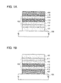
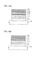
- a light-emitting element of one embodiment of the present invention which includes the fluorene compound described in Embodiment 1 for a hole-transport layer, will be described with reference to FIGS. 1A and 1B .
- an EL layer having at least a hole-transport layer and a light-emitting layer is interposed between a pair of electrodes.
- the EL layer may have a plurality of layers in addition to the hole-transport layer and the light-emitting layer.
- the plurality of layers has a structure in which a layer containing a substance having a high carrier-injection property and a layer containing a substance having a high carrier-transport property are combined and stacked so that a light-emitting region is formed in a region away from the electrodes, that is, so that carriers recombine in a region away from the electrodes.
- the plurality of layers may include, for example, a hole-injection layer, an electron-injection layer, an electron-transport layer, and the like.
- an EL layer 102 having a hole-transport layer 112 and a light-emitting layer 113 is provided between a pair of electrodes, a first electrode 101 and a second electrode 103.
- the EL layer 102 includes a hole-injection layer 111, the hole-transport layer 112, the light-emitting layer 113, an electron-transport layer 114, and an electron-injection layer 115.
- 1 A includes the first electrode 101 formed over a substrate 100, the hole-injection layer 111, the hole-transport layer 112, the light-emitting layer 113, the electron-transport layer 114, and the electron-injection layer 115 which are stacked over the first electrode 101 in this order, and the second electrode 103 provided thereover.
- the first electrode 101 functions as an anode and the second electrode 103 functions as a cathode.
- the substrate 100 is used as a support of the light-emitting element.
- the substrate 100 for example, glass, quartz, plastic, or the like can be used.
- a flexible substrate can also be used.
- the flexible substrate is a substrate that can be bent, such as a plastic substrate made of polycarbonate, polyarylate, or polyether sulfone, for example.
- a film made of polypropylene, polyester, vinyl, polyvinyl fluoride, vinyl chloride, or the like), an inorganic film formed by evaporation, or the like can also be used. Note that materials other than these can be used as long as they can function as a support of the light-emitting element.
- any of metals, alloys, conductive compounds, mixtures thereof, and the like which has a high work function is preferably used.
- Specific examples include indium oxide-tin oxide (ITO: indium tin oxide), indium oxide-tin oxide containing silicon or silicon oxide, indium oxide-zinc oxide (IZO: indium zinc oxide), indium oxide containing tungsten oxide and zinc oxide (IWZO), and the like.
- Films of these conductive metal oxides are usually formed by sputtering, but may be formed by application of a sol-gel method or the like.
- an IZO film can be formed by a sputtering method using a target obtained by adding 1 wt% to 20 wt% of zinc oxide to indium oxide.
- an IWZO film can be formed by a sputtering method using a target obtained by adding 0.5 wt% to 5 wt% of tungsten oxide and 0.1 wt% to 1 wt% of zinc oxide to indium oxide.
- Other examples are gold, platinum, nickel, tungsten, chromium, molybdenum, iron, cobalt, copper, palladium, nitrides of metal materials (e.g., titanium nitride), and the like.
- any of a variety of metals, alloys, and electrically conductive compounds, a mixture thereof, and the like can be used regardless of the work function; for example, aluminum, silver, an alloy containing aluminum (e.g., Al-Si), or the like can also be used.
- the EL layer 102 formed over the first electrode 101 has at least the hole-transport layer 112 and the light-emitting layer 113, and the hole-transport layer 112 includes a fluorene compound which is one embodiment of the present invention.
- a known substance can be used, and either a low molecular compound or a high molecular compound can be used.
- substances forming the EL layer 102 may consist of organic compounds or may include an inorganic compound as a part.
- the EL layer 102 is formed by stacking an appropriate combination of the hole-injection layer 111, the electron-transport layer 114, the electron-injection layer 115, and the like in addition to the hole-transport layer 112 and the light-emitting layer 113.
- the hole-injection layer 111 is a layer containing a substance having a high hole-injection property.
- a substance having a high hole-injection property which can be used are metal oxides, such as molybdenum oxide, titanium oxide, vanadium oxide, rhenium oxide, ruthenium oxide, chromium oxide, zirconium oxide, hafnium oxide, tantalum oxide, silver oxide, tungsten oxide, and manganese oxide.
- Other examples of a substance that can be used are phthalocyanine-based compounds, such as phthalocyanine (abbreviation: H 2 Pc) and copper(II) phthalocyanine (abbreviation: CuPc).
- aromatic amine compounds which are low molecular organic compounds, such as 4,4',4"-tris( N , N diphenylamino)triphenylamine (abbreviation: TDATA), 4,4',4"-tris[ N -(3-methylphenyl)-N-phenylamino]triphenylamine (abbreviation: MTDATA), 4,4'-bis[ N -(4-diphenylaminophenyl)- N -phenylamino]biphenyl (abbreviation: DPAB), 4,4'-bis( N - ⁇ 4-[ N '-(3-methylphenyl)- N '-phenylamino]phenyl ⁇ - N- phenylamino)biphenyl (abbreviation: DNTPD), 1,3,5-tris[ N -(4-diphenylaminophenyl)- N -phenylamino]benzene (abbreviation: TDATA), 4,4',
- a substance that can be used are high molecular compounds (e.g., oligomers, dendrimers, and polymers), such as poly( N -vinylcarbazole) (abbreviation: PVK), poly(4-vinyltriphenylamine) (abbreviation: PVTPA), poly[ N -(4- ⁇ N '-[4-(4-diphenylamino)phenyl]phenyl- N '-phenylamino ⁇ phenyl)methacryla mide] (abbreviation: PTPDMA), and poly[ N , N '-bis(4-butylphenyl)- N , N '-bis(phenyl)benzidine] (abbreviation: Poly-TPD), and high molecular compounds to which acid is added, such as poly(3,4-ethylenedioxythiophene)/poly(styrenesulfonic acid) (PEDOT/PSS), or polyaniline/poly
- the composite material formed by combining an organic compound and an electron acceptor may be used.
- an acceptor an acceptor
- the organic compound is preferably a material excellent in transporting the generated holes (a substance having a high hole-transport property).
- organic compound used for the composite material examples include a variety of compounds, such as aromatic amine compounds, carbazole derivatives, aromatic hydrocarbons, and high molecular compounds (e.g., oligomers, dendrimers, and polymers).
- the organic compound used for the composite material is preferably an organic compound having a high hole-transport property, and specifically preferably a substance having a hole mobility of 10 -6 cm 2 /Vs or more. Note that other than these substances, any substance that has a property of transporting more holes than electrons may be used.
- Organic compounds that can be used for the composite material will be specifically described below.
- a fluorene compound of one embodiment of the present invention is an organic compound having a high hole-transport property, and thus can be favorably used for the composite material.
- organic compound that can be used for the composite material are aromatic amine compounds, such as TDATA, MTDATA, DPAB, DNTPD, DPA3B, PCzPCA1, PCzPCA2, PCzPCN1, 4,4'-bis[ N -(1-naphthyl)- N -phenylamino]biphenyl (abbreviation: NPB or ⁇ -NPD), N , N '-bis(3-methylphenyl)- N , N '-diphenyl-[1,1'-biphenyl]-4,4'-diamine (abbreviation: TPD), and 4-phenyl-4'-(9-phenylfluoren-9-yl)triphenylamine (abbreviation: BPAFLP), and carbazole derivatives, such as 4,4'-di
- organic compound that can be used are aromatic hydrocarbon compounds, such as 2- tert -butyl-9,10-di(2-naphthyl)anthracene (abbreviation: t-BuDNA), 2- tert -butyl-9,10-di(1-naphthyl)anthracene, 9,10-bis(3,5-diphenylphenyl)anthracene (abbreviation: DPPA), 2- tert -butyl-9,10-bis(4-phenylphenyl)anthracene (abbreviation: t-BuDBA), 9,10-di(2-naphthyl)anthracene (abbreviation: DNA), 9,10-diphenylanthracene (abbreviation: DPAnth), 2- tert -butylanthracene (abbreviation: t-BuAnth), 9,10-bis(4-methyl-1-nap
- an organic compound that can be used are aromatic hydrocarbon compounds, such as 2,3,6,7-tetramethyl-9,10-di(2-naphthyl)anthracene, 9,9'-bianthryl, 10,10'-diphenyl-9,9'-bianthryl, 10,10' -bis(2-phenylphenyl)-9,9' -bianthryl, 10,10'-bis[(2,3,4,5,6-pentaphenyl)phenyl]-9,9'-bianthryl, anthracene, tetracene, rubrene, perylene, 2,5,8,11-tetra( tert -butyl)perylene, pentacene, coronene, 4,4'-bis(2,2-diphenylvinyl)biphenyl (abbreviation: DPVBi), and 9,10-bis[4-(2,2-diphenylvinyl)phenyl]anthracene (abbreviation: DPVP), 2,
- examples of the electron acceptor are organic compounds, such as 7,7,8,8-tetracyano-2,3,5,6-tetrafluoroquinodimethane (abbreviation: F 4 -TCNQ) and chloranil, oxides of transition metals, and oxides of metals that belong to Groups 4 to 8 in the periodic table, and the like.
- Specific preferred examples include vanadium oxide, niobium oxide, tantalum oxide, chromium oxide, molybdenum oxide, tungsten oxide, manganese oxide, and rhenium oxide because their electron-acceptor properties are high.
- molybdenum oxide is especially preferable since it is stable in the air, has low hygroscopic property, and is easily treated.
- the composite material may be formed using the above-described electron acceptor and the above-described high molecular compound such as PVK, PVTPA, PTPDMA, or Poly-TPD, and may be used for the hole-injection layer 111.
- the hole-transport layer 112 is a layer that contains a substance having a high hole-transport property.
- the hole-transport layer 112 of this embodiment includes a fluorene compound of one embodiment of the present invention.
- the light-emitting layer 113 is a layer including a light-emitting substance.
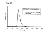
- a fluorescent compound which emits fluorescence
- a phosphorescent compound which emits phosphorescence
- a fluorene compound of one embodiment of the present invention is a material which emits fluorescence, and thus can be used as the light-emitting substance.
- the following light-emitting materials can be given, for example: materials that emit blue light, such as N , N' -bis[4-(9 H -carbazol-9-yl)phenyl]- N , N' -diphenylstilbene-4,4'-diamine (abbreviation: YGA2S), 4-(9 H carbazol-9-yl)-4'-(10-phenyl-9-anthryl)triphenylamine (abbreviation: YGAPA), and 4-(10-phenyl-9-anthryl)-4'-(9-phenyl-9 H -carbazol-3-yl)triphenylamine (abbreviation: PCBAPA); materials that emit green light, such as N -(9,10-diphenyl-2-anthryl)- N ,9-diphenyl-9 H -carbazol-3-amine (abbreviation: 2PCAPA), N
- the following light-emitting materials can be given, for example: materials that emit blue light, such as bis[2-(4',6'-difluorophenyl)pyridinato- N , C 2' ]iridium(III)tetrakis(1-pyrazolyl)borate (abbreviation: FIr6), bis[2-(4',6'-difluorophenyl)pyridinato- N , C 2' ]iridium(III)picolinate (abbreviation: FIrpic), bis ⁇ 2-[3',5'-bis(trifluoromethyl)phenyl]pyridinato- N , C 2' ⁇ iridium(III)picolinate (abbreviation: Ir(CF 3 ppy) 2 (pic)), and bis[2-(4',6'-difluorophenyl)pyridinato- N
- materials that emit blue light such as bis[2-(4',6'-diflu
- any of the following rare-earth metal complexes can be used as a phosphorescent compound: tris(acetylacetonato)(monophenanthroline)terbium(III) (abbreviation: Tb(acac) 3 (Phen)); tris(1,3-diphenyl-1,3-propanedionato)(monophenanthroline)europium(III) (abbreviation: Eu(DBM) 3 (Phen)); and tris[1-(2-thenoyl)-3,3,3-trifluoroacetonato](monophenanthroline)europium(III) (abbreviation: Eu(TTA) 3 (Phen)), because their light emission is from a rare-earth metal ion (electronic transition between different multiplicities) in such a rare-earth metal complex.
- a high molecular compound can be used as the light-emitting substance.
- the following light-emitting materials can be given, for example: materials that emit blue light, such as poly(9,9-dioctylfluorene-2,7-diyl) (abbreviation: PFO), poly[(9,9-dioctylfluorene-2,7-diyl)- co -(2,5-dimethoxybenzene-1,4-diyl)] (abbreviation: PF-DMOP), and poly ⁇ (9,9-dioctyfluorene-2,7-diyl)- co -[ N , N '-di-(p-butylphenyl)-1,4-diaminobenzene] ⁇ (abbreviation: TAB-PFH); materials that emit green light, such as poly( p -phenylenevinylene) (abbreviation: PPV), poly(
- the light-emitting layer 113 may have a structure in which any of the above-described light-emitting substances (guest material) is dispersed into another substance (host material).
- guest material any of the above-described light-emitting substances
- host material another substance
- a variety of substances can be used as the host material, and it is preferable to use a substance having a LUMO level higher than that of a light-emitting substance and having a HOMO level lower than that of the light-emitting substance.
- a fluorene compound of one embodiment of the present invention is a substance having a high LUMO level and a low HOMO level, and thus can be favorably used as the host material.
- a host material thereof is preferably a substance having a T1 level higher than that of the light-emitting substance.
- a fluorene compound of one embodiment of the present invention is a substance having a high T1 level, and thus can be favorably used as a host material of a phosphorescent light-emitting substance.
- a host material thereof is preferably a substance having a level of singlet excitation enegy (S1 level) higher than that of the light-emitting substance.
- S1 level singlet excitation enegy
- a fluorene compound of one embodiment of the present invention is a substance having a high S1 level, and thus can be favorably used as a host material of a fluorescent light-emitting substance.
- the host material that can be used are the following materials: metal complexes, such as tris(8-quinolinolato)aluminum(III) (abbreviation: Alq), tris(4-methyl-8-quinolinolato)aluminum(III) (abbreviation: Almq 3 ), bis(10-hydroxybenzo[ h ]quinolinato)beryllium(II) (abbreviation: BeBq 2 ), bis(2-methyl-8-quinolinolato)(4-phenylphenolato)aluminum(III) (abbreviation: BAlq), bis(8-quinolinolato)zinc(II) (abbreviation: Znq), bis[2-(2-benzoxazolyl)phenolato]zinc(II) (abbreviation: ZnPBO), and bis[2-(2-benzothiazolyl)phenolato]zinc(II) (abbreviation: ZnBTZ); hetero
- Plural kinds of host materials can also be used.
- a substance such as rubrene which suppresses crystallization may be further added.
- NPB, Alq, or the like may be further added in order to efficiently transfer energy to the guest material.
- the electron-transport layer 114 is a layer including a substance having a high electron-transport property.
- the substance having a high electron-transport property are metal complexes having a quinoline skeleton or a benzoquinoline skeleton, such as tris(8-quinolinolato)aluminum (abbreviation: Alq), tris(4-methyl-8-quinolinolato)aluminum (abbreviation: Almq 3 ), bis(10-hydroxybenzo[ h ]quinolinato)beryllium (abbreviation: BeBq 2 ), and bis(2-methyl-8-quinolinolato)(4-phenylphenolato)aluminum (abbreviation: BAlq).
- Alq tris(8-quinolinolato)aluminum
- Almq 3 tris(4-methyl-8-quinolinolato)aluminum
- BeBq 2 bis(10-hydroxybenzo[ h ]quinolina
- metal complexes having an oxazole-based or thiazole-based ligand such as bis[2-(2-hydroxyphenyl)benzoxazolato]zinc (abbreviation: Zn(BOX) 2 ) and bis[2-(2-hydroxyphenyl)benzothiazolato]zinc (abbreviation: Zn(BTZ) 2 ).
- 2-(4-biphenylyl)-5-(4- tert -butylphenyl)-1,3,4-oxadiazole (abbreviation: PBD), 1,3-bis[5-( p - tert -butylphenyl)-1,3,4-oxadiazol-2-yl]benzene (abbreviation: OXD-7), 3-(4-biphenylyl)-4-phenyl-5-(4- tert -butylphenyl)-1,2,4-triazole (abbreviation: TAZ), bathophenanthroline (abbreviation: BPhen), bathocuproine (abbreviation: BCP), or the like can be used.
- the substances described here are mainly substances having an electron mobility of 10 -6 cm 2 /Vs or more. Further, the electron-transport layer is not limited to a single layer, and may be a stack of two or more layers containing any of the above substances.
- the electron-injection layer 115 is a layer that contains a substance having a high electron-injection property.
- the substance that can be used for the electron-injection layer 115 are alkali metals, alkaline earth metals, and compounds thereof, such as lithium, cesium, calcium, lithium fluoride, cesium fluoride, calcium fluoride, and lithium oxide, rare earth-metal compounds, such as erbium fluoride, and the above-mentioned substances for forming the electron-transport layer 114.
- a composite material formed by combining an organic compound and an electron donor may be used for the electron-injection layer 115.
- a composite material in which electrons are generated in the organic compound by the electron donor, has high electron-injection and electron-transport properties.
- the organic compound here is preferably a material excellent in transporting the generated electrons, and specifically any of the above substances (such as metal complexes and heteroaromatic compounds) for the electron-transport layer 114 can be used.
- the electron donor can be a substance exhibiting an electron-donating property for the organic compound. Specific examples of the electron donor are alkali metals, alkaline earth metals, and rare earth-metals, such as lithium, cesium, magnesium, calcium, erbium, and ytterbium.
- alkali metal oxides and alkaline earth metal oxides are preferable, examples of which are lithium oxide, calcium oxide, barium oxide, and the like, and a Lewis base such as magnesium oxide or an organic compound such as tetrathiafulvalene (abbreviation: TTF) can be used.
- a Lewis base such as magnesium oxide or an organic compound such as tetrathiafulvalene (abbreviation: TTF) can be used.
- the hole-injection layer 111, the hole-transport layer 112, the light-emitting layer 113, the electron-transport layer 114, and the electron-injection layer 115 which are described above can each be formed by a method, such as an evaporation method (e.g., a vacuum evaporation method), an inkjet method, or a coating method.
- a method such as an evaporation method (e.g., a vacuum evaporation method), an inkjet method, or a coating method.
- any of metals, alloys, conductive compounds, mixtures thereof, and the like which has a low work function (specifically, a work function of 3.8 eV or less) is preferably used for the second electrode 103.
- the substance that can be used are elements that belong to Groups 1 and 2 in the periodic table, that is, alkali metals such as lithium and cesium, alkaline earth metals such as magnesium, calcium, and strontium, alloys thereof (e.g., Mg-Ag and Al-Li), rare earth-metals such as europium and ytterbium, alloys thereof, aluminum, silver, and the like.
- a layer included in the EL layer 102 and formed in contact with the second electrode 103 is formed using the composite material formed by combining the organic compound and the electron donor (the donor), which are described above, a variety of conductive materials, such as aluminum, silver, ITO, and indium oxide-tin oxide containing silicon or silicon oxide, can be used regardless of the work function.
- a vacuum evaporation method or a sputtering method can be used.
- a coating method, an inkjet method, or the like can be used.
- a current flows due to a potential difference generated between the first electrode 101 and the second electrode 103 and holes and electrons recombine in the EL layer 102, so that light is emitted. Then, this light emission is extracted outside through one or both of the first electrode 101 and the second electrode 103. Therefore, one or both of the first electrode 101 and the second electrode 103 are electrodes having a property of transmitting visible light.
- the structure of the layers provided between the first electrode 101 and the second electrode 103 is not limited to the above-described structure.
- a structure other than the above may alternatively be employed as long as a light-emitting region in which holes and electrons recombine is provided in a portion away from the first electrode 101 and the second electrode 103 so as to prevent quenching due to proximity of the light-emitting region to metal.
- a layer including a substance having a high electron-transport property, a substance having a high hole-transport property, a substance having a high electron-injection property, a substance having a high hole-injection property, a bipolar substance (a substance having a high electron-transport property and a high hole-transport property), a hole-blocking material, or the like may freely be combined with a light-emitting layer and a hole-transport layer including a fluorene compound of one embodiment of the present invention.
- a fluorene compound of one embodiment of the present invention is a substance having a low HOMO level, and thus can be favorably used as a hole-blocking material.
- the EL layer 102 is provided between a pair of electrodes, the first electrode 101 and the second electrode 103, over the substrate 100.
- the EL layer 102 includes the hole-injection layer 111, the hole-transport layer 112, the light-emitting layer 113, the electron-transport layer 114, and the electron-injection layer 115.
- the light-emitting element in FIG. 1B is provided between a pair of electrodes, the first electrode 101 and the second electrode 103, over the substrate 100.
- the EL layer 102 includes the hole-injection layer 111, the hole-transport layer 112, the light-emitting layer 113, the electron-transport layer 114, and the electron-injection layer 115.
- 1B includes the second electrode 103 serving as a cathode over the substrate 100, the electron-injection layer 115, the electron-transport layer 114, the light-emitting layer 113, the hole-transport layer 112, and the hole-injection layer 111 which are stacked over the second electrode 103 in this order, and the first electrode 101 provided thereover which serves as an anode.
- a light-emitting element of this embodiment includes a fluorene compound of one embodiment of the present invention in a hole-transport layer; however, a light-emitting element of the present invention is not limited to this structure.
- a fluorene compound of one embodiment of the present invention may be included in a hole-injection layer of a light-emitting element.
- a hole-transport layer may be formed using a fluorene compound of one embodiment of the present invention, or may be formed using another material having a high hole-transport property.
- a fluorene compound of one embodiment of the present invention may be used as a host material of a fluorescent light-emitting material or a phosphorescent light-emitting material which emits phosphorescence to green.
- a fluorene compound of one embodiment of the present invention has a low HOMO level, a high LUMO level, and a wide band gap.
- a carrier-transport layer such as a hole-transport layer, an electron-transport layer, or a hole-blocking layer
- a highly efficient element can be obtained.
- the EL layer is interposed between the pair of electrodes.
- the EL layer includes at least a hole-transport layer and a light-emitting layer, and the hole-transport layer includes a fluorene compound of one embodiment of the present invention. Further, the EL layer may include a hole-injection layer, an electron-transport layer, or an electron-injection layer in addition to the light-emitting layer and the hole-transport layer.
- the electrodes (the first electrode and the second electrode) and the EL layer may be formed by any of a wet process such as a droplet discharging method (an inkjet method), a spin coating method, or a printing method, or by a dry process such as a vacuum evaporation method, a CVD method, or a sputtering method.
- a wet process allows formation at atmospheric pressure with a simple apparatus and by a simple process, which gives the effects of simplifying the process and improving productivity.
- a dry process does not need dissolution of a material and enables use of a material that has low solubility in a solution, which expands the range of material choices.
- All the thin films included in the light-emitting element may be formed by a wet process.
- the light-emitting element can be manufactured with only facilities needed for a wet process.
- the following method may be employed: formation of the stacked layers up to formation of the light-emitting layer is performed by a wet process whereas a functional layer, the first electrode, and the like which are stacked over the light-emitting layer are formed by a dry process.
- the second electrode and a functional layer are formed by a dry process before the formation of the light-emitting layer whereas the light-emitting layer, a functional layer stacked thereover, and the first electrode are formed by a wet process.
- this embodiment is not limited to these, and a light-emitting element can be formed by appropriate selection from a wet process and a dry process depending on a material to be used, necessary film thickness, and the interface state.
- a light-emitting element is fabricated over a substrate made of glass, plastic, or the like.
- a passive matrix light-emitting device can be manufactured.
- a light-emitting element may be fabricated in such a way that a thin film transistor (TFT), for example, is formed over a substrate made of glass, plastic, or the like and the light-emitting element is formed over an electrode electrically connected to the TFT.
- TFT thin film transistor
- a staggered TFT or an inverted staggered TFT may be employed.
- crystallinity of a semiconductor used for the TFT an amorphous semiconductor or a crystalline semiconductor may be used.
- a driver circuit formed over a TFT substrate may be formed with both n-channel TFTs and p-channel TFTs or may be formed with either n-channel TFTs or p-channel TFTs.
- a light-emitting element can be manufactured using a fluorene compound of one embodiment of the present invention. According to one embodiment of the present invention, a light-emitting element having high emission efficiency can be realized. In addition, a light-emitting element having a long lifetime can be realized.
- a light-emitting device (an image display device) including a light-emitting element of one embodiment of the present invention which is obtained as above can realize low power consumption.
- a passive matrix light-emitting device or an active matrix light-emitting device in which driving of the light-emitting element is controlled by a thin film transistor (TFT) can be manufactured.
- This embodiment can be implemented in appropriate combination with any of the other embodiments.
- This light-emitting element is a light-emitting element including a plurality of light-emitting units between a first electrode and a second electrode.
- a first light-emitting unit 311 and a second light-emitting unit 312 are stacked between a first electrode 301 and a second electrode 303.
- the first electrode 301 functions as an anode
- the second electrode 303 functions as a cathode.
- the first electrode 301 and the second electrode 303 can be similar to those in Embodiment 2.
- the first light-emitting unit 311 and the second light-emitting unit 312 may have the same or different structures.
- the first light-emitting unit 311 and the second light-emitting unit 312 may have the same structure as in Embodiment 2, or either of the units may differ in structure from that in Embodiment 2.
- a charge-generation layer 313 is provided between the first light-emitting unit 311 and the second light-emitting unit 312.
- the charge-generation layer 313 has a function of injecting electrons into one of the light-emitting units and injecting holes into the other of the light-emitting units when a voltage is applied between the first electrode 301 and the second electrode 303.
- the charge-generation layer 313 injects electrons into the first light-emitting unit 311 and injects holes into the second light-emitting unit 312.
- the charge-generation layer 313 preferably has a property of transmitting visible light in terms of light extraction efficiency. Further, the charge-generation layer 313 functions even if it has lower conductivity than the first electrode 301 or the second electrode 303.
- the charge-generation layer 313 may have a structure in which it includes the organic compound having a high hole-transport property and the electron acceptor (the acceptor) or a structure in which it includes an organic compound having a high electron-transport property and the electron donor (the donor), or may be a stack of both of these structures.
- the electron acceptor or the electron donor is at least capable of providing and receiving electrons with the assistance of an electric field.
- a fluorene compound of one embodiment of the present invention can be used as the organic compound having a high hole-transport property.
- Other examples are aromatic amine compounds, such as NPB, TPD, TDATA, MTDATA, and 4,4'-bis[ N -(spiro-9,9'-bifluoren-2-yl)- N -phenylamino]biphenyl (abbreviation: BSPB), and the like.
- the substances mentioned here are mainly substances that have a hole mobility of 10 -6 cm 2 /Vs or more. Note that other than the above substances, any organic compound that has a property of transporting more holes than electrons may be used.
- Examples of the electron acceptor are 7,7,8,8-tetracyano-2,3,5,6-tetrafluoroquinodimethane (abbreviation: F 4 -TCNQ), chloranil, oxides of transition metals, and oxides of metals that belong to Groups 4 to 8 in the periodic table, and the like.
- Specific preferred examples include vanadium oxide, niobium oxide, tantalum oxide, chromium oxide, molybdenum oxide, tungsten oxide, manganese oxide, and rhenium oxide because their electron-acceptor properties are high.
- molybdenum oxide is especially preferable since it is stable in the air, has low hygroscopic property, and is easily treated.
- any of the following substances can be used as the organic compound having a high electron-transport property, for example: metal complexes having a quinoline skeleton or a benzoquinoline skeleton such as Alq, Almq 3 , BeBq 2 , and BAlq; metal complexes having an oxazole-based ligand or a thiazole-based ligand, such as Zn(BOX) 2 and Zn(BTZ) 2 ; and the like.
- metal complexes are PBD, OXD-7, TAZ, BPhen, BCP, and the like.
- the substances described here are mainly substances having an electron mobility of 10 -6 cm 2 /Vs or more. Note that other than the above substances, any organic compound that has a property of transporting more electrons than holes may be used.
- Examples of the electron donor that can be used are alkali metals, alkaline-earth metals, rare-earth metals, metals that belong to Group 13 in the periodic table and oxides or carbonates thereof, and preferably specifically lithium, cesium, magnesium, calcium, ytterbium, indium, lithium oxide, cesium carbonate, and the like.
- An organic compound, such as tetrathianaphthacene, may be used as the electron donor.
- the charge-generation layer 313 By forming the charge-generation layer 313 with any of the above materials, it is possible to suppress an increase in driving voltage caused when the EL layers are stacked.
- the embodiment can be applied to a light-emitting element in which three or more light-emitting units are stacked as illustrated in FIG. 2B .
- a plurality of light-emitting units which is partitioned by a charge-generation layer is arranged between a pair of electrodes, as in the light-emitting element according to this embodiment, whereby it is possible to realize an element having a long lifetime which can emit light with a high luminance while current density is kept low.
- emission colors of the light-emitting units different, light having a desired color can be obtained from the light-emitting element as a whole.
- the emission colors of first and second light-emitting units are complementary in a light-emitting element having the two light-emitting units, so that the light-emitting element can be made to emit white light as a whole.
- the term "complementary" means color relationship in which an achromatic color is obtained when colors are mixed. That is, emission of white light can be obtained by mixture of light emitted from substances whose emission colors are complementary colors. Further, the same applies to a light-emitting element having three light-emitting units.
- the light-emitting element as a whole can emit white light when the emission color of the first light-emitting unit is red, the emission color of the second light-emitting unit is green, and the emission color of the third light-emitting unit is blue.
- FIG. 3A is a top view illustrating the light-emitting device
- FIG. 3B is a cross-sectional view taken along lines A-B and C-D of FIG. 3A .
- reference numeral 401 denotes a driver circuit portion (a source side driver circuit)
- reference numeral 402 denotes a pixel portion
- reference numeral 403 denotes a driver circuit portion (a gate side driver circuit), which are each indicated by dotted lines.
- Reference numeral 404 denotes a sealing substrate
- reference numeral 405 denotes a sealing material
- a portion enclosed by the sealing material 405 is a space 407.
- a lead wiring 408 is a wiring for transmitting signals that are to be input to the source side driver circuit 401 and the gate side driver circuit 403, and receives a video signal, a clock signal, a start signal, a reset signal, and the like from a flexible printed circuit (FPC) 409 which serves as an external input terminal.
- FPC flexible printed circuit
- PWB printed wiring board
- the light-emitting device in this specification includes not only a light-emitting device itself but also a light-emitting device to which an FPC or a PWB is attached.
- the driver circuit portion and the pixel portion are formed over an element substrate 410.
- the source side driver circuit 401 which is the driver circuit portion and one pixel in the pixel portion 402 are illustrated.
- CMOS circuit which includes an n-channel TFT 423 and a p-channel TFT 424 is formed.
- the driver circuit may be any of a variety of circuits formed with TFTs, such as a CMOS circuit, a PMOS circuit, or an NMOS circuit.
- CMOS circuit a driver-integrated type in which a driver circuit is formed over the substrate
- PMOS circuit a PMOS circuit
- NMOS circuit NMOS circuit
- the pixel portion 402 includes a plurality of pixels having a switching TFT 411, a current control TFT 412, and a first electrode 413 electrically connected to a drain of the current control TFT 412.
- an insulator 414 is formed to cover an end portion of the first electrode 413.
- the insulator 414 is formed by using a positive type photosensitive acrylic resin film.
- the insulator 414 is provided such that either an upper end portion or a lower end portion of the insulator 414 has a curved surface with a curvature.
- a curvature For example, when positive photosensitive acrylic is used as a material for the insulator 414, it is preferable that only an upper end portion of the insulator 414 have a curved surface with a radius of curvature (0.2 ⁇ m to 3 ⁇ m).
- An EL layer 416 and a second electrode 417 are formed over the first electrode 413.
- a material for forming the first electrode 413 functioning as the anode a material having a high work function is preferably used.
- a single layer of an ITO film an indium tin oxide film that includes silicon, an indium oxide film that includes 2 wt% to 20 wt% of zinc oxide, a titanium nitride film, a chromium film, a tungsten film, a Zn film, a Pt film, or the like, a stacked layer of a titanium nitride film and a film that mainly includes aluminum, a three-layer structure of a titanium nitride film, a film that mainly includes aluminum, and a titanium nitride film, or the like. Note that, when a stacked layer structure is employed, resistance of a wiring is low and an excellent ohmic contact is obtained.
- the EL layer 416 is formed by any of various methods such as an evaporation method using an evaporation mask, a droplet discharging method like an inkjet method, a printing method, and a spin coating method.
- the EL layer 416 includes a fluorene compound described in Embodiment 1.
- another material included in the EL layer 416 may be a low molecular material, an oligomer, a dendrimer, a high molecular material, or the like.
- the second electrode 417 As a material used for the second electrode 417 which is formed over the EL layer 416 and serves as a cathode, it is preferable to use a material having a low work function (e.g., Al, Mg, Li, Ca, or an alloy or a compound thereof such as Mg-Ag, Mg-In, or Al-Li).
- a stack of a metal thin film having a reduced thickness and a transparent conductive film e.g., ITO, indium oxide containing 2 wt% to 20 wt% of zinc oxide, indium oxide-tin oxide that includes silicon or silicon oxide, or zinc oxide
- ITO transparent conductive film
- the sealing substrate 404 is attached to the element substrate 410 with the sealing material 405, so that a light-emitting element 418 is provided in the space 407 enclosed by the element substrate 410, the sealing substrate 404, and the sealing material 405.
- the space 407 is filled with a filler, and may be filled with an inert gas (such as nitrogen or argon) or the sealing material 405.
- an epoxy-based resin is preferably used as the sealing material 405.
- a material used for the sealing substrate 404 a plastic substrate formed of fiberglass-reinforced plastics (FRP), polyvinyl fluoride (PVF), polyester, acrylic, or the like can be used other than a glass substrate or a quartz substrate.
- the active matrix light-emitting device including the light-emitting element of one embodiment of the present invention can be obtained.
- FIGS. 4A and 4B illustrate a perspective view and a cross-sectional view of a passive matrix light-emitting device including a light-emitting element of the present invention. Note that FIG. 4A is a perspective view of the light-emitting device, and FIG. 4B is a cross-sectional view taken along line X-Y of FIG. 4A .
- an EL layer 504 is provided between a first electrode 502 and a second electrode 503 over a substrate 501.
- An end portion of the first electrode 502 is covered with an insulating layer 505.
- a partition layer 506 is provided over the insulating layer 505.
- the sidewalls of the partition layer 506 slope so that a distance between both the sidewalls is gradually narrowed toward the surface of the substrate.
- a cross section taken along the direction of the short side of the partition layer 506 is trapezoidal, and the base (side in contact with the insulating layer 505) is shorter than the upper side (side not in contact with the insulating layer 505).
- the passive matrix light-emitting device including a light-emitting element of one embodiment of the present invention can be obtained.
- the light-emitting devices described in this embodiment are both formed using a light-emitting element of one embodiment of the present invention, and accordingly, the light-emitting devices have low power consumption.
- Examples of the electronic devices to which the light-emitting device is applied are television devices (also referred to as TV or television receivers), monitors for computers and the like, cameras such as digital cameras and digital video cameras, digital photo frames, cellular phones (also referred to as portable telephone devices), portable game machines, portable information terminals, audio playback devices, large game machines such as pin-ball machines, and the like. Specific examples of these electronic devices and a lighting device are illustrated in FIGS. 5A to 5E .
- FIG. 5A illustrates an example of a television device.
- a display portion 7103 is incorporated in a housing 7101.
- the display portion 7103 is capable of displaying images, and a light-emitting device can be used for the display portion 7103.
- the housing 7101 is supported by a stand 7105.
- the television device 7100 can be operated with an operation switch of the housing 7101 or a separate remote controller 7110. With operation keys 7109 of the remote controller 7110, channels and volume can be controlled and images displayed on the display portion 7103 can be controlled. Furthermore, the remote controller 7110 may be provided with a display portion 7107 for displaying data output from the remote controller 7110.
- the television device 7100 is provided with a receiver, a modem, and the like. With the receiver, general television broadcasting can be received. Furthermore, when the television device 7100 is connected to a communication network by wired or wireless connection via the modem, one-way (from a transmitter to a receiver) or two-way (between a transmitter and a receiver, between receivers, or the like) data communication can be performed.
- FIG. 5B illustrates a computer, which includes a main body 7201, a housing 7202, a display portion 7203, a keyboard 7204, an external connection port 7205, a pointing device 7206, and the like.
- This computer is manufactured by using a light-emitting device for the display portion 7203.
- FIG. 5C illustrates a portable game machine, which includes two housings, a housing 7301 and a housing 7302, connected with a joint portion 7303 so that the portable game machine can be opened or closed.
- a display portion 7304 is incorporated in the housing 7301 and a display portion 7305 is incorporated in the housing 7302.
- 5C includes a speaker portion 7306, a recording medium insertion portion 7307, an LED lamp 7308, an input means (an operation key 7309, a connection terminal 7310, a sensor 7311 (a sensor having a function of measuring force, displacement, position, speed, acceleration, angular velocity, rotational frequency, distance, light, liquid, magnetism, temperature, chemical substance, sound, time, hardness, electric field, current, voltage, electric power, radiation, flow rate, humidity, gradient, oscillation, odor, or infrared rays), and a microphone 7312), and the like.
- a sensor 7311 a sensor having a function of measuring force, displacement, position, speed, acceleration, angular velocity, rotational frequency, distance, light, liquid, magnetism, temperature, chemical substance, sound, time, hardness, electric field, current, voltage, electric power, radiation, flow rate, humidity, gradient, oscillation, odor, or infrared rays
- a microphone 7312 and the like.
- the structure of the portable game machine is not limited to the above as long as a light-emitting device is used for at least either the display portion 7304 or the display portion 7305, or both, and may include other accessories as appropriate.
- the portable game machine illustrated in FIG. 5C has a function of reading out a program or data stored in a storage medium to display it on the display portion, and a function of sharing information with another portable game machine by wireless communication.
- the portable game machine illustrated in FIG. 5C can have a variety of functions without limitation to the above.
- FIG. 5D illustrates an example of a cellular phone.
- the cellular phone 7400 is provided with operation buttons 7403, an external connection port 7404, a speaker 7405, a microphone 7406, and the like, in addition to a display portion 7402 incorporated in a housing 7401. Note that the cellular phone 7400 is manufactured using a light-emitting device for the display portion 7402.
- the first mode is a display mode mainly for displaying an image.
- the second mode is an input mode mainly for inputting information such as characters.
- the third mode is a display-and-input mode in which two modes of the display mode and the input mode are mixed.
- a character input mode mainly for inputting characters is selected for the display portion 7402 so that characters displayed on a screen can be input.
- a detection device including a sensor for detecting inclination, such as a gyroscope or an acceleration sensor, is provided inside the cellular phone 7400
- display on the screen of the display portion 7402 can be automatically changed by determining the orientation of the cellular phone 7400 (whether the cellular phone is placed horizontally or vertically for a landscape mode or a portrait mode).
- the screen modes are switched by touch on the display portion 7402 or operation with the operation buttons 7403 of the housing 7401.
- the screen modes can be switched depending on kinds of images displayed on the display portion 7402. For example, when a signal for an image to be displayed on the display portion is data of moving images, the screen mode is switched to the display mode. When the signal is text data, the screen mode is switched to the input mode.
- the screen mode may be controlled so as to be switched from the input mode to the display mode.
- the display portion 7402 may function as an image sensor. For example, an image of a palm print, a fingerprint, or the like is taken by touch on the display portion 7402 with the palm or the finger, whereby personal identification can be performed. Furthermore, by provision of a backlight or a sensing light source emitting near-infrared light for the display portion, an image of a finger vein, a palm vein, or the like can also be taken.
- FIG. 5E illustrates a desk lamp, which includes a lighting portion 7501, a shade 7502, an adjustable arm 7503, a support 7504, a base 7505, and a power switch 7506.
- the desk lamp is manufactured using a light-emitting device for the lighting portion 7501.
- the "lighting device” also includes ceiling lights, wall lights, and the like.
- FIG. 6 illustrates an example in which a light-emitting device is used for an interior lighting device 801. Since the light-emitting device can have a larger area, it can be used as a lighting device having a large area. Furthermore, the light-emitting device can be used as a roll-type lighting device 802. As illustrated in FIG. 6 , a desk lamp 803 described with reference to FIG. 5E may also be used in a room provided with the interior lighting device 801.
- electronic devices or lighting devices can be obtained by application of a light-emitting device.
- Application range of the light-emitting device is so wide that the light-emitting device can be applied to electronic devices in a variety of fields.
- the Rf values of the substance that was the object of the synthesis and 9-(4-bromophenyl)-9-phenyl-9 H -fluorene were respectively 0.33 and 0.60, which were found by silica gel thin layer chromatography (TLC) (with a developing solvent of ethyl acetate and hexane in a 1:10 ratio).
- This compound was identified as DBTFLP-III, which was the object of the synthesis, by nuclear magnetic resonance (NMR) spectroscopy.
- FIGS. 7A and 7B are shown in FIGS. 7A and 7B .
- FIG. 7B is a chart where the range of from 6.0 ppm to 9.0 ppm in FIG. 7A is enlarged.
- FIG. 8A shows the absorption spectrum of DBTFLP-III in a toluene solution of DBTFLP-III
- FIG. 8B shows the emission spectrum thereof
- FIG. 9A shows the absorption spectrum of a thin film of DBTFLP-III
- FIG. 9B shows the emission spectrum thereof.
- An ultraviolet-visible spectrophotometer V-550, manufactured by JASCO Corporation was used for the measurements. Samples were prepared in such a way that the solution was put in a quartz cell and the thin film was formed on a quartz substrate by evaporation.
- the horizontal axis represents wavelength (nm) and the vertical axis represents absorption intensity (arbitrary unit).
- the horizontal axis represents wavelength (nm) and the vertical axis represents emission intensity (arbitrary unit).
- FIG. 8A and FIG. 9A show that DBTFLP-III is a substance having weak absorption in the visible region.
- DBTFLP-III which is a fluorene compound of one embodiment of the present invention is used for a light-emitting element, visible light emitted from a light-emitting layer is unlikely to be absorbed by DBTFLP-III, and thus a decrease in light extraction efficiency of the element can be suppressed.
- DBTFLP-III has a peak of the emission spectrum at a very short wavelength and thus can be used for a host material of a light-emitting layer or used for a carrier-transport layer adjacent to the light-emitting layer in a fluorescent element which emits visible light.
- the potential of the working electrode with respect to the reference electrode was scanned from 0.00 V to 1.25 V and then from 1.25 V to 0.00 V.
- the HOMO level was found to be -6.20 eV.
- the oxidation peak was at a similar value even after 100 cycles. This indicates that DBTFLP-III has properties effective against repetition of redox reactions between an oxidized state and a neutral state.
- a potential energy (eV) of the reference electrode (Ag/Ag + electrode), which was used in this example, with respect to the vacuum level was calculated. That is, the Fermi level of the Ag/Ag + electrode was calculated. It is known that the oxidation-reduction potential of ferrocene in methanol is +0.610 [V vs. SHE] with respect to the normal hydrogen electrode (Reference: Christian R. Goldsmith et al., J. Am. Chem. Soc., Vol. 124, No. 1, 83-96, 2002 ). On the other hand, using the reference electrode used in this example, the oxidation-reduction potential of ferrocene in methanol was calculated to be +0.11 V [vs. Ag/Ag + ]. Therefore, it is found that the potential energy of the reference electrode used in this example was lower than that of the normal hydrogen electrode by 0.50 [eV].
- a solution used for the CV measurement dehydrated dimethylformamide (DMF, manufactured by Sigma-Aldrich Inc., 99.8 %, Catalog No. 22705-6) was used as a solvent, and tetra- n -butylammonium perchlorate ( n -Bu 4 NClO 4 , manufactured by Tokyo Chemical Industry Co., Ltd., Catalog No. T0836), which was a supporting electrolyte, was dissolved in the solvent such that the concentration of tetra- n -butylammonium perchlorate was 100 mmol/L. Further, the object to be measured was dissolved in the solvent such that the concentration thereof was 2 mmol/L.
- DMF dehydrated dimethylformamide
- n -Bu 4 NClO 4 manufactured by Tokyo Chemical Industry Co., Ltd., Catalog No. T0836
- a platinum electrode (PTE platinum electrode, manufactured by BAS Inc.) was used as a working electrode
- a platinum electrode (Pt counter electrode for VC-3 (5 cm), manufactured by BAS Inc.) was used as an auxiliary electrode
- an Ag/Ag + electrode (RE-7 reference electrode for nonaqueous solvent, manufactured by BAS Inc.) was used as a reference electrode. Note that the measurement was conducted at room temperature (20 °C to 25 °C). In addition, the scan rate at the CV measurement was set to 0.1 V/sec in all the measurement.
- FIG. 14 shows results of the CV measurement of the oxidation characteristics.
- the oxidation peak potential (from the neutral state to the oxidation state) E pa was 1.18 V.
- the reduction peak potential (from the oxidation state to the neutral state) E pc was 1.04 V. Therefore, a half-wave potential (an intermediate potential between E pa and E pc , ( E pa + E pc )/2 [V]) can be calculated to be 1.11 V. This shows that DBTFLP-III is oxidized with an electrical energy of 1.11 [V vs. Ag/Ag + ].
- a thin film of DBTFLP-III was formed by vacuum evaporation. This thin film was not a white and opaque film but a transparent film. This also suggests that DBTFLP-III is a substance which is unlikely to be crystallized.
- the Rf values of the substance that was the object of the synthesis and 9-(4-bromophenyl)-9-phenyl-9 H -fluorene were respectively 0.40 and 0.48, which were found by silica gel thin layer chromatography (TLC) (with a developing solvent of ethyl acetate and hexane in a 1:10 ratio).
- This compound was identified as DBTFLP-IV, which was the object of the synthesis, by nuclear magnetic resonance (NMR) spectroscopy.
- FIGS. 10A and 10B are shown in FIGS. 10A and 10B .
- FIG. 10B is a chart where the range of from 6.5 ppm to 8.5 ppm in FIG. 10A is enlarged.
- FIG. 11A shows the absorption spectrum of DBTFLP-IV in a hexane solution of DBTFLP-IV
- FIG. 11B shows the emission spectrum of DBTFLP-IV in a toluene solution of DBTFLP-IV
- FIG. 12A shows the absorption spectrum of a thin film of DBTFLP-IV
- FIG. 12B shows the emission spectrum thereof.
- An ultraviolet-visible spectrophotometer V-550, manufactured by JASCO Corporation was used for the measurements. Samples were prepared in such a way that the solution was put in a quartz cell and the thin film was formed on a quartz substrate by evaporation.
- the horizontal axis represents wavelength (nm) and the vertical axis represents absorption intensity (arbitrary unit).
- the horizontal axis represents wavelength (nm) and the vertical axis represents emission intensity (arbitrary unit).
- FIG. 11A and FIG. 12A show that DBTFLP-IV is a substance having weak absorption in the visible region.
- DBTFLP-IV which is a fluorene compound of one embodiment of the present invention is used for a light-emitting element, visible light emitted is unlikely to be reabsorbed, and thus the element is unlikely to have a decrease in light extraction efficiency.
- DBTFLP-IV has a peak of the emission spectrum at a very short wavelength and thus can be used as a host material of a light-emitting layer or used for a carrier-transport layer adjacent to the light-emitting layer in a fluorescent element which emits visible light.
- the potential of the working electrode with respect to the reference electrode was scanned from -0.40 V to 1.50 V and then from 1.50 V to -0.40 V.
- the HOMO level was found to be -6.20 eV.
- the oxidation peak was at a similar value even after 100 cycles. This indicates that DBTFLP-IV has properties effective against repetition of redox reactions between an oxidized state and a neutral state.
- the potential of the working electrode with respect to the reference electrode was scanned from -3.00 V to -1.18 V and then from -1.18 V to -3.00 V.
- the LUMO level was found to be -2.19 eV.
- the reduction peak was at a similar value even after 100 cycles. This indicates that DBTFLP-IV has properties effective against repetition of redox reactions between a neutral state and a reduced state.
- Example 1 can be referred to for details.
- the glass transition temperature was measured with a differential scanning calorimeter (Pyris 1 DSC, manufactured by Perkin Elmer Co., Ltd.). According to the measurement results, it was found that the glass transition temperature was 154 °C. In this manner, DBTFLP-IV has a high glass transition temperature and excellent heat resistance. In addition, the crystallization peak does not exist; thus, it is found that DBTFLP-IV is a substance which is unlikely to be crystallized. This can be attributed to a steric molecular structure and a sufficiently high molecular weight (576.7) of DBTFLP-IV.
- a thin film of DBTFLP-IV was formed by vacuum evaporation. This thin film was not a white and opaque film but a transparent film. This also suggests that DBTFLP-IV is a substance which is unlikely to be crystallized.
- DBTFLP-IV is found to be a material having a wide band gap and excellent thermophysical properties, and also an electrochemically stable material.
- a film of indium tin oxide containing silicon oxide (ITSO) was formed over a glass substrate 1100 by a sputtering method, so that a first electrode 1101 was formed. Note that the thickness was set to 110 nm and the electrode area was set to 2 mm ⁇ 2 mm.
- ITSO indium tin oxide containing silicon oxide
- UV ozone treatment was performed for 370 seconds after washing of a surface of the substrate with water and baking that was performed at 200 °C for one hour.
- the substrate was transferred into a vacuum evaporation apparatus where the pressure had been reduced to approximately 10 -4 Pa, and subjected to vacuum baking at 170 °C for 30 minutes in a heating chamber of the vacuum evaporation apparatus, and then the substrate 1100 was cooled down for about 30 minutes.
- the substrate 1100 provided with the first electrode 1101 was fixed to a substrate holder in the vacuum evaporation apparatus so that a surface on which the first electrode 1101 was provided faced downward.
- the pressure in the vacuum evaporation apparatus was reduced to about 10 -4 Pa.
- 4-[4-(9-phenyl-9 H -fluoren-9-yl)phenyl]-6-phenyldibenzothiophene (abbreviation: DBTFLP-IV) synthesized in Example 2 and molybdenum(VI) oxide were co-evaporated to form a hole-injection layer 1111 over the first electrode 1101.
- the co-evaporation method refers to an evaporation method in which evaporation is carried out from a plurality of evaporation sources at the same time in one treatment chamber.
- a DBTFLP-IV film was formed to a thickness of 10 nm to form a hole-transport layer 1112.
- mDBTPTp-II 4-[3-(triphenylen-2-yl)phenyl]dibenzothiophene (abbreviation: mDBTPTp-II) and tris(2-phenylpyridinato- N , C 2' )iridium(III) (abbreviation: Ir(ppy) 3 ) were co-evaporated to form a light-emitting layer 1113 over the hole-transport layer 1112.
- the thickness of the light-emitting layer 1113 was set to 40 nm.
- a film of tris(8-quinolinolato)aluminum (abbreviation: Alq) was formed to a thickness of 15 nm to form a first electron-transport layer 1114a.
- a bathophenanthroline (abbreviation: BPhen) film was formed to a thickness of 15 nm to form a second electron-transport layer 1114b.
- a lithium fluoride (LiF) film was formed by evaporation to a thickness of 1 nm to form an electron-injection layer 1115.
- Light-Emitting Element 1 of this example was fabricated.
- Table 1 shows an element structure of Light-Emitting Element 1 obtained as described above.
- Light-Emitting Element 1 was sealed so as not to be exposed to air. Then, operation characteristics of Light-Emitting Element 1 were measured. Note that the measurements were carried out at room temperature (in the atmosphere kept at 25 °C).
- FIG. 15 shows the voltage-luminance characteristics of Light-Emitting Element 1.
- the horizontal axis represents voltage (V) and the vertical axis represents luminance (cd/m 2 ).
- FIG. 16 shows the luminance-current efficiency characteristics.
- the horizontal axis represents luminance (cd/m 2 ) and the vertical axis represents current efficiency (cd/A).
- Table 2 shows the voltage (V), current density (mA/cm 2 ), CIE chromaticity coordinates (x, y), current efficiency (cd/A), power efficiency (lm/W), and external quantum efficiency (%) of Light-Emitting Element 1 at a luminance of 1000 cd/m 2 .
- FIG. 17 shows the emission spectrum of Light-emitting Element 1 which was obtained by applying a current at a current density of 0.1 mA/cm 2 .
- the horizontal axis represents wavelength (nm) and the vertical axis represents intensity (arbitrary unit).
- the emission spectrum of Light-Emitting Element 1 has a peak at 516 nm.
- Light-Emitting Element 1 was found to provide green light emission originating from Ir(ppy) 3 .
- FIG. 18 shows the luminance-chromaticity coordinate characteristics.
- the horizontal axis represents luminance (cd/m 2 ) and the vertical axis represents chromaticity coordinate (the x-coordinate or the y-coordinate).
- Light-Emitting Element 1 shows substantially no change in color over a range from low luminance to high luminance. It can be said from this result that Light-Emitting Element 1 is an element having excellent carrier balance.
- a substance having a sufficiently high T1 level for a hole-transport layer which is in contact with the light-emitting layer it is preferable to use a substance having a sufficiently high T1 level for a hole-transport layer which is in contact with the light-emitting layer.
- a layer including a fluorene compound of one embodiment of the present invention is in contact with a light-emitting layer which emits green light, and as shown in FIG. 16 and Table 2, Light-Emitting Element 1 is found to have high emission efficiency.
- a fluorene compound of one embodiment of the present invention is found to have a sufficiently high T1 level (which is at least higher than that of a green light-emitting material).
- an element having high emission efficiency can be realized by use of a fluorene compound of one embodiment of the present invention for a hole-transport layer.
- This can be attributed to a sufficiently high LUMO level of a fluorene compound of one embodiment of the present invention and suppressed passage of electrons through a light-emitting layer. It can also be attributed to a sufficiently low HOMO level and an excellent property of injecting holes into a light-emitting layer.
- a fluorene compound of one embodiment of the present invention can be favorably used for a hole-transport layer of a light-emitting element which includes a green phosphorescent compound in a light-emitting layer.
- the findings also suggest that a composite material formed by combining a fluorene compound of one embodiment of the present invention and an electron acceptor (an acceptor) can be favorably used for a hole-injection layer. This can be attributed to a composite material including a fluorene compound of one embodiment of the present invention which is a material having a high hole-injection property and a high hole-transport property.
- a film of ITSO was formed over a glass substrate 1100 by a sputtering method, so that a first electrode 1101 was formed. Note that the thickness was set to 110 nm and the electrode area was set to 2 mm ⁇ 2 mm.
- UV ozone treatment was performed for 370 seconds after washing of a surface of the substrate with water and baking that was performed at 200 °C for one hour.
- the substrate was transferred into a vacuum evaporation apparatus where the pressure had been reduced to approximately 10 -4 Pa, and subjected to vacuum baking at 170 °C for 30 minutes in a heating chamber of the vacuum evaporation apparatus, and then the substrate 1100 was cooled down for about 30 minutes.
- the substrate 1100 provided with the first electrode 1101 was fixed to a substrate holder in the vacuum evaporation apparatus so that a surface on which the first electrode 1101 was provided faced downward.
- the pressure in the vacuum evaporation apparatus was reduced to about 10 -4 Pa.
- DBTFLP-IV synthesized in Example 2 and molybdenum(VI) oxide were co-evaporated to form a hole-injection layer 1111 over the first electrode 1101.
- a DBTFLP-IV film was formed to a thickness of 10 nm to form a hole-transport layer 1112.
- CzPA 9-[4-( N -carbazolyl)]phenyl-10-phenylanthracene
- 1,6FLPAPrn N,N '-bis[4-(9-phenyl-9 H -fluoren-9-yl)phenyl]- N , N '-diphenylpyrene-1,6-diamine
- the thickness of the light-emitting layer 1113 was set to 30 nm.
- a film of CzPA was formed to a thickness of 10 nm to form a first electron-transport layer 1114a.
- a BPhen film was formed to a thickness of 15 nm to form a second electron-transport layer 1114b.
- a LiF film was formed by evaporation to a thickness of 1 nm to form an electron-injection layer 1115.
- Light-Emitting Element 2 of this example was fabricated.
- a hole-injection layer 1111 of Comparative Light-Emitting Element 3 was formed by co-evaporating 9-phenyl-3-[4-(10-phenyl-9-anthryl)phenyl]-9H-carbazole (abbreviation: PCzPA) and molybdenum(VI) oxide.
- a hole-transport layer 1112 of Comparative Light-Emitting Element 3 was formed by forming a film of PCzPA to a thickness of 10 nm. Components other than the hole-injection layer 1111 and the hole-transport layer 1112 were manufactured in a manner similar to those of Light-Emitting Element 2.
- Table 3 shows element structures of Light-Emitting Element 2 and Comparative Light-Emitting Element 3 obtained as described above.
- these light-emitting elements were sealed so as not to be exposed to air. Then, operation characteristics of these light-emitting elements were measured. Note that the measurements were carried out at room temperature (in the atmosphere kept at 25 °C).
- Light-Emitting Element 2 and Comparative Light-Emitting Element 3 were formed over the same substrate.
- the first electrodes and the light-emitting layers to the second electrodes of the above-described two light-emitting elements were formed at the same respective times, and sealing was performed at the same time.
- FIG. 19 shows the luminance-current efficiency characteristics of Light-Emitting Element 2 and Comparative Light-Emitting Element 3.
- the horizontal axis represents luminance (cd/m 2 ) and the vertical axis represents current efficiency (cd/A).
- Table 4 shows the voltage (V), current density (mA/cm 2 ), CIE chromaticity coordinates (x, y), luminance (cd/m 2 ), current efficiency (cd/A), power efficiency (lm/W), and external quantum efficiency (%) of each light-emitting element at a luminance of around 1000 cd/m 2 .
- FIG. 20 shows the emission spectra of these light-emitting elements which were obtained by applying a current at a current density of 0.1 mA/cm 2 .
- the horizontal axis represents wavelength (nm) and the vertical axis represents intensity (arbitrary unit).
- the emission spectra of Light-Emitting Element 2 and Comparative Light-Emitting Element 3 at around 1000 cd/m 2 each have a peak at around 466 nm and are similar to each other.
- PCzPA used in Comparative Light-Emitting Element 3 in this example is one of materials which can realize a highly efficient, long-life light-emitting element when used as a material for a hole-transport layer or a material for a hole-injection layer. As can be seen from FIG. 19 , Light-Emitting Element 2 has higher emission efficiency than Comparative Light-Emitting Element 3.
- an element having high emission efficiency can be realized by use of a fluorene compound of one embodiment of the present invention for a hole-transport layer.
- This can be attributed to a sufficiently high LUMO level of a fluorene compound of one embodiment of the present invention and suppressed passage of electrons through a light-emitting layer. It can also be attributed to a sufficiently low HOMO level and an excellent property of injecting holes into a light-emitting layer.
- a substance having a sufficiently high level of singlet excitation energy for a hole-transport layer which is in contact with the light-emitting layer.
- S1 level singlet excitation energy
- a layer including a fluorene compound of one embodiment of the present invention is in contact with a light-emitting layer which emits blue light, and as shown in FIG. 19 and Table 4, Light-Emitting Element 2 is found to have high emission efficiency.
- a fluorene compound of one embodiment of the present invention is found to have a sufficiently high S1 level.
- the singlet excitation energy refers to an energy difference between a ground state and a singlet excited state.
- Light-Emitting Element 2 and Comparative Light-Emitting Element 3 were subjected to reliability tests.
- the two light-emitting elements of this example were each driven under the conditions where the initial luminance was set to 5000 cd/m 2 and the current density was constant.
- Light-Emitting Element 2 and Comparative Light-Emitting Element 3 kept 65 % of the initial luminance after the driving for 100 hours.
- PCzPA used in Comparative Light-Emitting Element 3 is one of materials which can realize a long-life light-emitting element when used as a material for a hole-transport layer or a material for a hole-injection layer. This result indicates that an element including a fluorene compound of one embodiment of the present invention can also achieve a long lifetime.
- Light-Emitting Element 2 including a fluorene compound of one embodiment of the present invention in a composite material of a hole-injection layer and in a hole-transport layer is an element which has comparably high reliability and extremely high emission efficiency as compared to Comparative Light-Emitting Element 3.
- a film of ITSO was formed over a glass substrate 1100 by a sputtering method, so that a first electrode 1101 was formed. Note that the thickness was set to 110 nm and the electrode area was set to 2 mm x 2 mm.
- UV ozone treatment was performed for 370 seconds after washing of a surface of the substrate with water and baking that was performed at 200 °C for one hour.
- the substrate was transferred into a vacuum evaporation apparatus where the pressure had been reduced to approximately 10 -4 Pa, and subjected to vacuum baking at 170 °C for 30 minutes in a heating chamber of the vacuum evaporation apparatus, and then the substrate 1100 was cooled down for about 30 minutes.
- the substrate 1100 provided with the first electrode 1101 was fixed to a substrate holder in the vacuum evaporation apparatus so that a surface on which the first electrode 1101 was provided faced downward.
- the pressure in the vacuum evaporation apparatus was reduced to about 10 -4 Pa.
- 2,8-diphenyl-4-[4-(9-phenyl-9 H -fluoren-9-yl)phenyl]dibenzothiophene (abbreviation: DBTFLP-III) synthesized in Example 1 and molybdenum(VI) oxide were co-evaporated to form a hole-injection layer 1111 over the first electrode 1101.
- a DBTFLP-III film was formed to a thickness of 10 nm to form a hole-transport layer 1112.
- CzPA and 1,6FLPAPrn were co-evaporated to form a light-emitting layer 1113 over the hole-transport layer 1112.
- the thickness of the light-emitting layer 1113 was set to 30 nm.
- a film of CzPA was formed to a thickness of 10 nm to form a first electron-transport layer 1114a.
- a BPhen film was formed to a thickness of 15 nm to form a second electron-transport layer 1114b.
- a LiF film was formed by evaporation to a thickness of 1 nm to form an electron-injection layer 1115.
- Light-Emitting Element 4 of this example was fabricated.
- a hole-injection layer 1111 of Comparative Light-Emitting Element 5 was formed by co-evaporating PCzPA and molybdenum(VI) oxide.
- a hole-transport layer 1112 of Comparative Light-Emitting Element 5 was formed using PCzPA. The thickness was set to be 10 nm. Components other than the hole-injection layer 1111 and the hole-transport layer 1112 were manufactured in a manner similar to those of Light-Emitting Element 4.
- Table 5 shows element structures of Light-Emitting Element 4 and Comparative Light-Emitting Element 5 obtained as described above.
- these light-emitting elements were sealed so as not to be exposed to air. Then, operation characteristics of these light-emitting elements were measured. Note that the measurements were carried out at room temperature (in the atmosphere kept at 25 °C).
- Light-Emitting Element 4 and Comparative Light-Emitting Element 5 were formed over the same substrate.
- the first electrodes and the light-emitting layers to the second electrodes of the above-described two light-emitting elements were formed at the same respective times, and sealing was performed at the same time.
- FIG. 21 shows the current density-luminance characteristics of Light-Emitting Element 4 and Comparative Light-Emitting Element 5.
- the horizontal axis represents current density (mA/cm 2 ) and the vertical axis represents luminance (cd/m 2 ).
- FIG. 22 shows the luminance-current efficiency characteristics.
- the horizontal axis represents luminance (cd/m 2 ) and the vertical axis represents current efficiency (cd/A).
- Table 6 shows the voltage (V), current density (mA/cm 2 ), CIE chromaticity coordinates (x, y), luminance (cd/m 2 ), current efficiency (cd/A), power efficiency (lm/W), and external quantum efficiency (%) of each light-emitting element at a luminance of around 1000 cd/m 2 .
- FIG. 23 shows the emission spectra of Light-Emitting Element 4 and Comparative Light-Emitting Element 5 which were obtained by applying a current at a current density of 0.1 mA/cm 2 .
- the horizontal axis represents wavelength (nm) and the vertical axis represents intensity (arbitrary unit).
- the emission spectra of Light-Emitting Element 4 and Comparative Light-Emitting Element 5 at around 1000 cd/m 2 each have a peak at around 466 nm and are similar to each other.
- Light-Emitting Element 4 exhibits higher emission efficiency than Comparative Light-Emitting Element 5.
- an element having high emission efficiency can be realized by use of a fluorene compound of one embodiment of the present invention for a hole-transport layer.
- This can be attributed to a sufficiently high LUMO level of a fluorene compound of one embodiment of the present invention and suppressed passage of electrons through a light-emitting layer. It can also be attributed to a sufficiently low HOMO level and an excellent property of injecting holes into a light-emitting layer.
- a layer including a fluorene compound of one embodiment of the present invention is in contact with a light-emitting layer which emits blue light, and as shown in FIG. 21, FIG. 22 , and Table 6, Light-Emitting Element 4 is found to have high emission efficiency.
- a fluorene compound of one embodiment of the present invention is found to have a sufficiently high S1 level (which is at least higher than that of a blue light-emitting material).
- the Rf value of the substance that was the object of the synthesis was 0.33, which was found by silica gel thin layer chromatography (TLC) (with a developing solvent of ethyl acetate and hexane in a 1:10 ratio).
- This compound was identified as mmDBFFLBi-II, which was the object of the synthesis, by nuclear magnetic resonance (NMR) spectroscopy.
- FIGS. 24A and 24B are shown in FIGS. 24A and 24B .
- FIG. 24B is a chart where the range of from 7.0 ppm to 8.2 ppm in FIG. 24A is enlarged.
- FIG. 25A shows the absorption spectrum of mmDBFFLBi-II in a toluene solution of mmDBFFLBi-II
- FIG. 25B shows the emission spectrum thereof
- FIG. 26A shows the absorption spectrum of a thin film of mmDBFFLBi-II
- FIG. 26B shows the emission spectrum thereof.
- An ultraviolet-visible spectrophotometer V-550, manufactured by JASCO Corporation was used for the measurements. Samples were prepared in such a way that the solution was put in a quartz cell and the thin film was formed on a quartz substrate by evaporation.
- the horizontal axis represents wavelength (nm) and the vertical axis represents absorption intensity (arbitrary unit).
- the horizontal axis represents wavelength (nm) and the vertical axis represents emission intensity (arbitrary unit).
- FIG. 25A and FIG. 26A show that mmDBFFLBi-II is a substance having weak absorption in the visible region.
- mmDBFFLBi-II which is a fluorene compound of one embodiment of the present invention is used for a light-emitting element, visible light emitted is unlikely to be reabsorbed, and thus the element is unlikely to have a decrease in light extraction efficiency.
- mmDBFFLBi-II has a peak of the emission spectrum at a very short wavelength and thus can be used as a host material of a light-emitting layer or used for a carrier-transport layer adjacent to the light-emitting layer in a fluorescent element which emits visible light.
- mmDBFFLBi-II A thin film of mmDBFFLBi-II was formed by vacuum evaporation. This thin film was not a white and opaque film but a transparent film. This also suggests that mmDBFFLBi-II is a substance which is unlikely to be crystallized.
- the Rf value of the substance that was the object of the synthesis was 0.25, which was found by silica gel thin layer chromatography (TLC) (with a developing solvent of ethyl acetate and hexane in a 1:10 ratio).
- This compound was identified as mmDBTFLBi-II, which was the object of the synthesis, by nuclear magnetic resonance (NMR) spectroscopy.
- FIGS. 27A and 27B are shown in FIGS. 27A and 27B .
- FIG. 27B is a chart where the range of from 7.0 ppm to 8.5 ppm in FIG. 27A is enlarged.
- FIG. 28A shows the absorption spectrum of mmDBTFLBi-II in a toluene solution of mmDBTFLBi-II
- FIG. 28B shows the emission spectrum thereof.
- An ultraviolet-visible spectrophotometer V-550, manufactured by JASCO Corporation
- V-550 ultraviolet-visible spectrophotometer
- a sample was prepared in such a way that the solution was put in a quartz cell.
- the absorption spectrum which was obtained by subtracting the absorption spectra of quartz and toluene from those of quartz and the solution.
- the horizontal axis represents wavelength (nm) and the vertical axis represents absorption intensity (arbitrary unit).
- FIG. 28A shows that mmDBTFLBi-II is a substance having weak absorption in the visible region.
- mmDBTFLBi-II which is a fluorene compound of one embodiment of the present invention is used for a light-emitting element, visible light emitted is unlikely to be reabsorbed, and thus the element is unlikely to have a decrease in light extraction efficiency.
- mmDBTFLBi-II has a peak of the emission spectrum at a very short wavelength and thus can be used as a host material of a light-emitting layer or used for a carrier-transport layer adjacent to the light-emitting layer in a fluorescent element which emits visible light.
- Step 4 Synthesis of 4-(3- ⁇ 9-[4-(9-phenylanthracen-10-yl)phenyl]-9 H -fluoren-9-yl ⁇ phenyl)dibenzofuran (abbreviation: mDBFFLPPhA-II) ⁇
- the recrystallized filtrate was purified by high performance liquid column chromatography (abbreviation: HPLC) (a developing solvent: chloroform). The obtained fraction was concentrated to give a light-yellow solid. The substances obtained by recrystallization and purified by high performance liquid column chromatography were combined to give 1.3 g of a light-yellow solid in a yield of 69 %.
- the obtained light-yellow solid was sublimated and purified by a train sublimation method.
- the light-yellow solid was heated at 300 °C under a pressure of 2.5 Pa with a flow rate of argon gas of 5 mL/min.
- a light-yellow solid was obtained in a yield of 94 %.
- a reaction scheme of the above synthesis method is illustrated in the following (H-4).
- This compound was identified as mDBFFLPPhA-II, which was the object of the synthesis, by nuclear magnetic resonance (NMR) spectroscopy.
- FIGS. 29A and 29B are shown in FIGS. 29A and 29B .
- FIG. 29B is a chart where the range of from 7.0 ppm to 8.2 ppm in FIG. 29A is enlarged.
- FIG. 30A shows the absorption spectrum of mDBFFLPPhA-II in a toluene solution of mDBFFLPPhA-II
- FIG. 30B shows the emission spectrum thereof
- FIG. 31A shows the absorption spectrum of a thin film of mDBFFLPPhA-II
- FIG. 31B shows the emission spectrum thereof.
- An ultraviolet-visible spectrophotometer V-550, manufactured by JASCO Corporation was used for the measurements. Samples were prepared in such a way that the solution was put in a quartz cell and the thin film was formed on a quartz substrate by evaporation.
- the horizontal axis represents wavelength (nm) and the vertical axis represents absorption intensity (arbitrary unit).
- the horizontal axis represents wavelength (nm) and the vertical axis represents emission intensity (arbitrary unit).
- mDBFFLPPhA-II is a substance having weak absorption in the visible region.
- mDBFFLPPhA-II which is a fluorene compound of one embodiment of the present invention is used for a light-emitting element, visible light emitted is unlikely to be reabsorbed, and thus the element is unlikely to have a decrease in light extraction efficiency.
- mDBFFLPPhA-II has a peak of the emission spectrum at a very short wavelength and thus can be used as a host material of a light-emitting layer or used for a carrier-transport layer adjacent to the light-emitting layer in a fluorescent element which emits visible light.
- mDBFFLPPhA-II has high emission intensity and can be used as a light-emitting material.
- a thin film of mDBFFLPPhA-II was formed by vacuum evaporation. This thin film was not a white and opaque film but a transparent film. This also suggests that mDBFFLPPhA-II is a substance which is unlikely to be crystallized.
- a light-emitting element of one embodiment of the present invention will be described with reference to FIG. 13A .
- the chemical formulae of materials used in this example are illustrated below. Note that the chemical formulae of materials which are already illustrated will be omitted.
- a film of ITSO was formed over a glass substrate 1100 by a sputtering method, so that a first electrode 1101 was formed. Note that the thickness was set to 110 nm and the electrode area was set to 2 mm x 2 mm.
- UV ozone treatment was performed for 370 seconds after washing of a surface of the substrate with water and baking that was performed at 200 °C for one hour.
- the substrate was transferred into a vacuum evaporation apparatus where the pressure had been reduced to approximately 10 -4 Pa, and subjected to vacuum baking at 170 °C for 30 minutes in a heating chamber of the vacuum evaporation apparatus, and then the substrate 1100 was cooled down for about 30 minutes.
- the substrate 1100 provided with the first electrode 1101 was fixed to a substrate holder in the vacuum evaporation apparatus so that a surface on which the first electrode 1101 was provided faced downward.
- the pressure in the vacuum evaporation apparatus was reduced to about 10 -4 Pa.
- PCzPA and molybdenum(VI) oxide were co-evaporated to form a hole-injection layer 1111 over the first electrode 1101.
- a PCzPA film was formed to a thickness of 10 nm to form a hole-transport layer 1112.
- mDBFFLPPhA-II 4-(3- ⁇ 9-[4-(9-phenylanthracen-10-yl)phenyl]-9 H -fluoren-9-yl ⁇ phenyl)dibenzofuran (abbreviation: mDBFFLPPhA-II) synthesized in Example 8 and 1,6FLPAPrn were co-evaporated to form a light-emitting layer 1113 oer the hole-transport layer 1112.
- the thickness of the light-emitting layer 1113 was set to 30 nm.
- a film of Alq was formed to a thickness of 10 nm to form a first electron-transport layer 1114a.
- a BPhen film was formed to a thickness of 15 nm to form a second electron-transport layer 1114b.
- a LiF film was formed by evaporation to a thickness of 1 nm to form an electron-injection layer 1115.
- Table 7 shows an element structure of Light-Emitting Element 6 obtained as described above.
- Light-Emitting Element 6 was sealed so as not to be exposed to air. Then, operation characteristics of Light-Emitting Element 6 were measured. Note that the measurements were carried out at room temperature (in the atmosphere kept at 25 °C).
- FIG. 32 shows the voltage-luminance characteristics of Light-Emitting Element 6.
- the horizontal axis represents voltage (V) and the vertical axis represents luminance (cd/m 2 ).
- FIG. 33 shows the voltage-current efficiency characteristics.
- the horizontal axis represents voltage (V) and the vertical axis represents current (mA).
- FIG. 34 shows the luminance-chromaticity coordinate characteristics.
- the horizontal axis represents luminance (cd/m 2 ) and the vertical axis represents chromaticity coordinate (the x-coordinate or the y-coordinate).
- FIG. 35 shows the luminance-external quantum efficiency characteristics. In FIG.
- the horizontal axis represents luminance (cd/m 2 ) and the vertical axis represents external quantum efficiency (%).
- Table 8 shows the voltage (V), current density (mA/cm 2 ), CIE chromaticity coordinates (x, y), luminance (cd/m 2 ), current efficiency (cd/A), power efficiency (lm/W), and external quantum efficiency (%) of Light-Emitting Element 6 at a luminance of 820 cd/m 2 .
- FIG. 36 shows the emission spectrum of Light-Emitting Element 6 which was obtained by applying a current at a current density of 1 mA/cm 2 .
- the horizontal axis represents wavelength (nm) and the vertical axis represents intensity (arbitrary unit).
- the emission spectrum of Light-Emitting Element 6 has a peak at around 466 nm.
- FIG. 32, FIG. 33 , and FIG. 35 show that Light-Emitting Element 6 has high emission efficiency, low driving voltage, and low power consumption.
- FIG. 34 shows that Light-Emitting Element 6 has a small change in chromaticity according to luminance and has excellent carrier balance.
- Light-Emitting Element 6 was driven under the conditions where the initial luminance was set to 1000 cd/m 2 and the current density was constant.
- FIG. 37 shows that Light-Emitting Element 6 kept 83 % of the initial luminance after the driving for 270 hours. It is found that Light-Emitting Element 6 according to one embodiment of the present invention has long lifetime and high reliability.
- a fluorene compound of one embodiment of the present invention is found suitable for a host material of a light-emitting layer which emits blue light.
- a fluorene compound of one embodiment of the present invention is found to have a sufficiently high S 1 level (which is at least higher than that of a blue light-emitting material).
- a first electrode 1101, a hole-injection layer 1111, a hole-transport layer 1112, and a light-emitting layer 1113 were formed over a glass substrate 1100 under the same conditions as those of Light-Emitting Element 6 described in Example 9.
- a film of BPhen was formed to a thickness of 25 nm to form an electron-transport layer 1114.
- a LiF film was formed by evaporation to a thickness of 1 nm to form an electron-injection layer 1115.
- Light-Emitting Element 7 of this example was fabricated.
- Table 9 shows an element structure of Light-Emitting Element 7 obtained as described above.
- Light-Emitting Element 7 was sealed so as not to be exposed to air. Then, operation characteristics of Light-Emitting Element 7 were measured. Note that the measurements were carried out at room temperature (in the atmosphere kept at 25 °C).
- FIG. 38 shows the voltage-luminance characteristics of Light-Emitting Element 7.
- the horizontal axis represents voltage (V) and the vertical axis represents luminance (cd/m 2 ).
- FIG. 39 shows the voltage-current characteristics.
- the horizontal axis represents voltage (V) and the vertical axis represents current (mA).
- FIG. 40 shows the luminance-chromaticity coordinate characteristics.
- the horizontal axis represents luminance (cd/m 2 ) and the vertical axis represents chromaticity coordinate (the x-coordinate or the y-coordinate).
- FIG. 41 shows the luminance-external quantum efficiency characteristics. In FIG.
- the horizontal axis represents luminance (cd/m 2 ) and the vertical axis represents external quantum efficiency (%).
- Table 10 shows the voltage (V), current density (mA/cm 2 ), CIE chromaticity coordinates (x, y), luminance (cd/m 2 ), current efficiency (cd/A), power efficiency (lm/W), and external quantum efficiency (%) of Light-Emitting Element 7 at a luminance of 990 cd/m 2 .
- FIG. 42 shows the emission spectrum of Light-Emitting Element 7 which was obtained by applying a current at a current density of 1 mA/cm 2 .
- the horizontal axis represents wavelength (nm) and the vertical axis represents intensity (arbitrary unit).
- the emission spectrum of Light-Emitting Element 7 has a peak at around 466 nm.
- FIG. 38, FIG. 39 , and FIG. 41 show that Light-Emitting Element 7 has high emission efficiency, low driving voltage, and low power consumption.
- FIG. 40 shows that Light-Emitting Element 7 has a small change in chromaticity according to luminance and has excellent carrier balance.
- a fluorene compound of one embodiment of the present invention is found suitable for a host material of a light-emitting layer which emits blue light.
- a fluorene compound of one embodiment of the present invention is found to have a sufficiently high S1 level (which is at least higher than that of a blue light-emitting material).
- N N' -bis[4-(9-phenyl-9 H -fluoren-9-yl)phenyl]- N , N' -diphenylpyrene-1,6-diamine (abbreviation: 1,6FLPAPrn) used in the above examples will be described.
- the obtained compound was identified as N , N' -bis[4-(9-phenyl-9 H -fluoren-9-yl)phenyl]- N , N' -diphenylpyrene-1,6-diamine (abbreviation: 1,6FLPAPrn) by nuclear magnetic resonance (NMR) spectroscopy.
Landscapes
- Chemical & Material Sciences (AREA)
- Organic Chemistry (AREA)
- Engineering & Computer Science (AREA)
- Materials Engineering (AREA)
- Physics & Mathematics (AREA)
- Spectroscopy & Molecular Physics (AREA)
- Manufacturing & Machinery (AREA)
- Inorganic Chemistry (AREA)
- Optics & Photonics (AREA)
- Crystallography & Structural Chemistry (AREA)
- Electroluminescent Light Sources (AREA)
- Organic Low-Molecular-Weight Compounds And Preparation Thereof (AREA)
- Furan Compounds (AREA)
Applications Claiming Priority (2)
| Application Number | Priority Date | Filing Date | Title |
|---|---|---|---|
| JP2010200522 | 2010-09-08 | ||
| JP2011122811 | 2011-05-31 |
Publications (3)
| Publication Number | Publication Date |
|---|---|
| EP2428512A2 true EP2428512A2 (de) | 2012-03-14 |
| EP2428512A3 EP2428512A3 (de) | 2012-04-18 |
| EP2428512B1 EP2428512B1 (de) | 2014-10-22 |
Family
ID=44677596
Family Applications (1)
| Application Number | Title | Priority Date | Filing Date |
|---|---|---|---|
| EP11179794.0A Active EP2428512B1 (de) | 2010-09-08 | 2011-09-02 | Fluorenverbindung, lichtemittierendes Element, lichtemittierende Vorrichtung, elektronische Vorrichtung und Beleuchtungsvorrichtung. |
Country Status (6)
| Country | Link |
|---|---|
| US (2) | US8993127B2 (de) |
| EP (1) | EP2428512B1 (de) |
| JP (2) | JP5859780B2 (de) |
| KR (2) | KR101949692B1 (de) |
| CN (3) | CN110156583A (de) |
| TW (2) | TWI555740B (de) |
Cited By (6)
| Publication number | Priority date | Publication date | Assignee | Title |
|---|---|---|---|---|
| US9496505B2 (en) | 2010-10-04 | 2016-11-15 | Semiconductor Energy Laboratory Co., Ltd. | Composite material, light-emitting element, light-emitting device, electronic device, and lighting device |
| WO2017144863A1 (en) * | 2016-02-22 | 2017-08-31 | Cambridge Display Technology Limited | Compound, composition and organic light-emitting device |
| CN109503736A (zh) * | 2017-09-15 | 2019-03-22 | 常州强力先端电子材料有限公司 | 芴类光引发剂及包含其的光固化组合物 |
| WO2020120969A1 (en) | 2018-12-14 | 2020-06-18 | Sumitomo Chemical Co., Ltd | Composition and organic light-emitting device |
| WO2020127176A1 (en) * | 2018-12-20 | 2020-06-25 | Merck Patent Gmbh | Materials for electronic devices |
| US11903227B2 (en) | 2015-03-09 | 2024-02-13 | Semiconductor Energy Laboratory Co., Ltd. | Light-emitting element, display device, electronic device, and lighting device |
Families Citing this family (15)
| Publication number | Priority date | Publication date | Assignee | Title |
|---|---|---|---|---|
| EP2433929B1 (de) | 2010-09-27 | 2013-10-23 | Semiconductor Energy Laboratory Co, Ltd. | Organische Verbindung, lichtemittierendes Element, lichtemittierende Vorrichtung, elektronische Vorrichtung und Beleuchtungsvorrichtung |
| JP6117465B2 (ja) | 2010-10-29 | 2017-04-19 | 株式会社半導体エネルギー研究所 | カルバゾール化合物、有機半導体材料および発光素子用材料 |
| KR101950363B1 (ko) | 2010-10-29 | 2019-02-20 | 가부시키가이샤 한도오따이 에네루기 켄큐쇼 | 페난트렌 화합물, 발광 소자, 발광 장치, 전자 기기, 및 조명 장치 |
| KR101910030B1 (ko) | 2010-11-30 | 2018-10-19 | 가부시키가이샤 한도오따이 에네루기 켄큐쇼 | 벤조옥사졸 유도체, 발광 소자, 발광 장치, 전자기기 및 조명 장치 |
| US9059411B2 (en) | 2012-02-29 | 2015-06-16 | Semiconductor Energy Laboratory Co., Ltd. | Fluorene compound, light-emitting element, light-emitting device, electronic device, and lighting device |
| KR102198635B1 (ko) * | 2012-04-20 | 2021-01-05 | 가부시키가이샤 한도오따이 에네루기 켄큐쇼 | 유기 화합물, 발광 소자, 발광 장치, 전자 기기, 및 조명 장치 |
| US9577221B2 (en) * | 2012-09-26 | 2017-02-21 | Universal Display Corporation | Three stack hybrid white OLED for enhanced efficiency and lifetime |
| TWI633100B (zh) | 2013-07-19 | 2018-08-21 | 半導體能源研究所股份有限公司 | 有機化合物、發光元件、顯示器模組、照明模組、發光裝置、顯示裝置、照明設備及電子裝置 |
| EP3297978B1 (de) * | 2015-05-18 | 2020-04-01 | Merck Patent GmbH | Materialien für organische elektrolumineszenzvorrichtungen |
| EP3133666B1 (de) | 2015-08-21 | 2020-03-11 | Samsung Display Co., Ltd. | Organische lichtemittierende vorrichtung |
| KR101984244B1 (ko) | 2015-09-09 | 2019-05-30 | 삼성에스디아이 주식회사 | 유기 화합물, 유기 광전자 소자 및 표시 장치 |
| KR101924086B1 (ko) | 2016-02-26 | 2018-11-30 | 삼성에스디아이 주식회사 | 유기 화합물, 유기 광전자 소자 및 표시 장치 |
| KR102182179B1 (ko) * | 2018-03-16 | 2020-11-24 | 주식회사 엘지화학 | 잉크 조성물 및 유기 발광 소자의 제조방법 |
| CN117343078A (zh) | 2021-11-25 | 2024-01-05 | 北京夏禾科技有限公司 | 有机电致发光材料和器件 |
| KR20230082719A (ko) * | 2021-12-01 | 2023-06-09 | 삼성디스플레이 주식회사 | 발광 소자 및 발광 소자용 아민 화합물 |
Citations (2)
| Publication number | Priority date | Publication date | Assignee | Title |
|---|---|---|---|---|
| JP2010200522A (ja) | 2009-02-26 | 2010-09-09 | Aisin Seiki Co Ltd | 往復動駆動機構とその往復駆動機構を用いた蓄冷型冷凍機及び圧縮機 |
| JP2011122811A (ja) | 2009-11-13 | 2011-06-23 | Kiyoshi Imai | 温室の温湿度管理システム及び温湿度管理方法 |
Family Cites Families (38)
| Publication number | Priority date | Publication date | Assignee | Title |
|---|---|---|---|---|
| GB9615110D0 (en) | 1996-07-18 | 1996-09-04 | Post Office | Luminescing inks and use of such inks in coding and other marking operations |
| WO2001094452A2 (en) | 2000-06-08 | 2001-12-13 | Lord Corporation | Uv curable coating for golf balls |
| JP2003261472A (ja) * | 2002-03-07 | 2003-09-16 | Mitsui Chemicals Inc | 有機電界発光素子および新規炭化水素化合物 |
| EP1416028A1 (de) * | 2002-10-30 | 2004-05-06 | Covion Organic Semiconductors GmbH | Neues Verfahren zur Herstellung von Monomeren verwendbar für die Herstellung von Halbleiterpolymeren |
| JP4067414B2 (ja) * | 2003-01-22 | 2008-03-26 | 三井化学株式会社 | 非対称置換アントラセン化合物、および該非対称置換アントラセン化合物を含有する有機電界発光素子 |
| US20060105199A1 (en) | 2004-11-18 | 2006-05-18 | 3M Innovative Properties Company | Electroluminescent devices containing trans-1,2-bis(acenyl)ethylene compounds |
| US8007927B2 (en) * | 2007-12-28 | 2011-08-30 | Universal Display Corporation | Dibenzothiophene-containing materials in phosphorescent light emitting diodes |
| JP2007001895A (ja) * | 2005-06-22 | 2007-01-11 | Tosoh Corp | 燐光ホスト化合物及びそれを用いた有機電界発光素子 |
| US20070026348A1 (en) | 2005-08-01 | 2007-02-01 | Fuji Photo Film Co., Ltd. | Black and white photothermographic material and image forming method |
| WO2007126262A1 (en) | 2006-04-27 | 2007-11-08 | Kyungwon Enterprise Co., Ltd. | Anion receptor, and electrolyte using the same |
| CN101511967B (zh) | 2006-09-01 | 2015-11-25 | 纳幕尔杜邦公司 | 氟烯烃用的酚稳定剂 |
| KR100852987B1 (ko) * | 2007-04-03 | 2008-08-19 | 주식회사 진웅산업 | 유기 발광 화합물 및 이를 이용한 유기 전계 발광 소자 |
| JP5151219B2 (ja) | 2007-04-09 | 2013-02-27 | コニカミノルタビジネステクノロジーズ株式会社 | 電子写真感光体、画像形成方法及び画像形成装置 |
| US8399108B2 (en) * | 2007-05-28 | 2013-03-19 | Cheil Industries, Inc. | Material for organic electro-optical device having fluorene derivative compound and organic electro-optical device including the same |
| JP5127300B2 (ja) | 2007-05-28 | 2013-01-23 | キヤノン株式会社 | フルオレン化合物及びそれを用いた有機発光素子並びに表示装置 |
| EP2444470B1 (de) * | 2007-08-31 | 2016-10-26 | Semiconductor Energy Laboratory Co., Ltd. | Lichtemittierendes element, lichtemittierende vorrichtung und elektronisches gerät |
| WO2009066808A1 (en) | 2007-11-22 | 2009-05-28 | Gracel Display Inc. | Aromatic electroluminescent compounds with high efficiency and electroluminescent device using the same |
| EP2221896A4 (de) * | 2007-11-22 | 2012-04-18 | Idemitsu Kosan Co | Organisches el-element |
| JP5353186B2 (ja) | 2007-11-30 | 2013-11-27 | 住友化学株式会社 | アミン系高分子化合物及びそれを用いた発光素子 |
| JP5574598B2 (ja) * | 2007-12-03 | 2014-08-20 | 株式会社半導体エネルギー研究所 | キノキサリン誘導体、およびキノキサリン誘導体を用いた発光素子、発光装置、電子機器 |
| US8216753B2 (en) | 2007-12-13 | 2012-07-10 | E I Du Pont De Nemours And Company | Electroactive materials |
| US8067764B2 (en) | 2007-12-17 | 2011-11-29 | E. I. Du Pont De Nemours And Company | Electroactive materials |
| EP2229382B1 (de) | 2007-12-21 | 2012-07-18 | Semiconductor Energy Laboratory Co, Ltd. | Triazolderivat, lichtemittierendes element, lichtemittierende vorrichtung und elektronische vorrichtung |
| EP2091097A3 (de) | 2008-02-13 | 2013-05-15 | Semiconductor Energy Laboratory Co, Ltd. | Lichtemittierendes Element, lichtemittierende Vorrichtung und elektronische Vorrichtung |
| JP5461037B2 (ja) * | 2008-03-21 | 2014-04-02 | 大阪瓦斯株式会社 | 臭素含有フルオレン化合物の製造方法 |
| US20110105693A1 (en) | 2008-05-01 | 2011-05-05 | Kanata Chemical Technologies Inc. | Cationic transition-metal arene catalysts |
| EP2123733B1 (de) | 2008-05-13 | 2013-07-24 | Konica Minolta Holdings, Inc. | Organisches elektrolumineszentes Element, Anzeigevorrichtung und Beleuchtungsvorrichtung |
| JP5479759B2 (ja) * | 2008-09-05 | 2014-04-23 | 株式会社半導体エネルギー研究所 | ベンゾオキサゾール誘導体、発光素子用材料、発光素子、発光装置及び電子機器 |
| WO2010074087A1 (ja) * | 2008-12-26 | 2010-07-01 | 出光興産株式会社 | 有機エレクトロルミネッセンス素子用材料及び有機エレクトロルミネッセンス素子 |
| WO2010131930A2 (ko) | 2009-05-15 | 2010-11-18 | 제일모직 주식회사 | 유기광전소자용 화합물 및 이를 포함하는 유기광전소자 |
| KR102193512B1 (ko) | 2009-05-29 | 2020-12-21 | 가부시키가이샤 한도오따이 에네루기 켄큐쇼 | 화합물 |
| US8642190B2 (en) | 2009-10-22 | 2014-02-04 | Semiconductor Energy Laboratory Co., Ltd. | Fluorene derivative, light-emitting element, light-emitting device, electronic device, and lighting device |
| TWI591065B (zh) | 2010-03-01 | 2017-07-11 | 半導體能源研究所股份有限公司 | 雜環化合物、發光元件、發光裝置、電子裝置、及照明裝置 |
| US10570113B2 (en) | 2010-04-09 | 2020-02-25 | Semiconductor Energy Laboratory Co., Ltd. | Aromatic amine derivative, light-emitting element, light-emitting device, electronic device, and lighting device |
| JP5815280B2 (ja) | 2010-05-21 | 2015-11-17 | 株式会社半導体エネルギー研究所 | トリアゾール誘導体 |
| TWI567075B (zh) | 2010-06-15 | 2017-01-21 | 國立清華大學 | 6H-吲哚〔3,2-b〕喹喔啉衍生物及其有機發光二極體 |
| US8771843B2 (en) | 2010-08-27 | 2014-07-08 | Semiconductor Energy Laboratory Co., Ltd. | Fluorene derivative, organic compound, and light-emitting element, light-emitting device, and electronic device using the compound |
| US9067916B2 (en) | 2011-02-01 | 2015-06-30 | Semiconductor Energy Laboratory Co., Ltd. | Heterocyclic compound |
-
2011
- 2011-09-02 EP EP11179794.0A patent/EP2428512B1/de active Active
- 2011-09-05 KR KR1020110089386A patent/KR101949692B1/ko active Active
- 2011-09-06 TW TW100132100A patent/TWI555740B/zh not_active IP Right Cessation
- 2011-09-06 TW TW105111846A patent/TWI600649B/zh not_active IP Right Cessation
- 2011-09-06 JP JP2011193860A patent/JP5859780B2/ja active Active
- 2011-09-07 CN CN201910221478.XA patent/CN110156583A/zh active Pending
- 2011-09-07 US US13/227,022 patent/US8993127B2/en not_active Expired - Fee Related
- 2011-09-07 CN CN201110278052.1A patent/CN102408407B/zh active Active
- 2011-09-07 CN CN201510896713.5A patent/CN105481642B/zh active Active
-
2015
- 2015-03-25 US US14/668,239 patent/US9564597B2/en active Active
- 2015-12-17 JP JP2015246107A patent/JP6148716B2/ja not_active Expired - Fee Related
-
2019
- 2019-02-12 KR KR1020190016079A patent/KR102076488B1/ko active Active
Patent Citations (2)
| Publication number | Priority date | Publication date | Assignee | Title |
|---|---|---|---|---|
| JP2010200522A (ja) | 2009-02-26 | 2010-09-09 | Aisin Seiki Co Ltd | 往復動駆動機構とその往復駆動機構を用いた蓄冷型冷凍機及び圧縮機 |
| JP2011122811A (ja) | 2009-11-13 | 2011-06-23 | Kiyoshi Imai | 温室の温湿度管理システム及び温湿度管理方法 |
Non-Patent Citations (3)
| Title |
|---|
| CHEM. MATER., vol. 10, 1998, pages 2235 - 2250 |
| CHRISTIAN R. GOLDSMITH ET AL., J. AM. CHEM. SOC., vol. 124, no. 1, 2002, pages 83 - 96 |
| TOSHIHIRO OHNISHI, TAMAMI KOYAMA: "Kobunshi EL Zairyou [High Molecular EL Material", KYORITSU SHUPPAN, pages: 64 - 67 |
Cited By (9)
| Publication number | Priority date | Publication date | Assignee | Title |
|---|---|---|---|---|
| US9496505B2 (en) | 2010-10-04 | 2016-11-15 | Semiconductor Energy Laboratory Co., Ltd. | Composite material, light-emitting element, light-emitting device, electronic device, and lighting device |
| US11903227B2 (en) | 2015-03-09 | 2024-02-13 | Semiconductor Energy Laboratory Co., Ltd. | Light-emitting element, display device, electronic device, and lighting device |
| WO2017144863A1 (en) * | 2016-02-22 | 2017-08-31 | Cambridge Display Technology Limited | Compound, composition and organic light-emitting device |
| US11349086B2 (en) | 2016-02-22 | 2022-05-31 | Cambridge Display Technology Limited | Compound, composition and organic light-emitting device |
| CN109503736A (zh) * | 2017-09-15 | 2019-03-22 | 常州强力先端电子材料有限公司 | 芴类光引发剂及包含其的光固化组合物 |
| WO2020120969A1 (en) | 2018-12-14 | 2020-06-18 | Sumitomo Chemical Co., Ltd | Composition and organic light-emitting device |
| GB2579807A (en) * | 2018-12-14 | 2020-07-08 | Sumitomo Chemical Co | Composition and organic light-emitting device |
| WO2020127176A1 (en) * | 2018-12-20 | 2020-06-25 | Merck Patent Gmbh | Materials for electronic devices |
| US12219874B2 (en) | 2018-12-20 | 2025-02-04 | Merck Patent Gmbh | Materials for electronic devices |
Also Published As
| Publication number | Publication date |
|---|---|
| KR101949692B1 (ko) | 2019-02-19 |
| TWI555740B (zh) | 2016-11-01 |
| US8993127B2 (en) | 2015-03-31 |
| US9564597B2 (en) | 2017-02-07 |
| CN102408407A (zh) | 2012-04-11 |
| TW201627298A (zh) | 2016-08-01 |
| JP2013010730A (ja) | 2013-01-17 |
| TWI600649B (zh) | 2017-10-01 |
| TW201300372A (zh) | 2013-01-01 |
| JP2016128413A (ja) | 2016-07-14 |
| CN110156583A (zh) | 2019-08-23 |
| JP5859780B2 (ja) | 2016-02-16 |
| JP6148716B2 (ja) | 2017-06-14 |
| KR20190017850A (ko) | 2019-02-20 |
| CN102408407B (zh) | 2016-01-06 |
| KR20120025984A (ko) | 2012-03-16 |
| CN105481642B (zh) | 2019-04-12 |
| EP2428512A3 (de) | 2012-04-18 |
| EP2428512B1 (de) | 2014-10-22 |
| KR102076488B1 (ko) | 2020-02-12 |
| US20120061714A1 (en) | 2012-03-15 |
| US20150243899A1 (en) | 2015-08-27 |
| CN105481642A (zh) | 2016-04-13 |
Similar Documents
| Publication | Publication Date | Title |
|---|---|---|
| EP2428512B1 (de) | Fluorenverbindung, lichtemittierendes Element, lichtemittierende Vorrichtung, elektronische Vorrichtung und Beleuchtungsvorrichtung. | |
| US20210151694A1 (en) | Composite Material, Light-Emitting Element, Light-Emitting Device, Electronic Device, and Lighting Device | |
| US9406893B2 (en) | Heterocyclic compound, light-emitting element, light-emitting device, electronic device, and lighting device | |
| EP2433929B1 (de) | Organische Verbindung, lichtemittierendes Element, lichtemittierende Vorrichtung, elektronische Vorrichtung und Beleuchtungsvorrichtung | |
| EP2363398B1 (de) | Heterocyclische Verbindung, lichtemittierendes Element, lichtemittierende Vorrichtung, elektronische Vorrichtung und Beleuchtungsvorrichtung | |
| JP2022153377A (ja) | 発光素子、発光装置、電子機器及び照明装置 | |
| EP2065378B1 (de) | Chinoxalinderivat und lichtemittierendes Element, lichtemittierende Vorrichtung und elektronische Vorrichtung mit dem Chinoxalinderivat | |
| EP2330102B1 (de) | Heterocyclische Verbindung, lichtemittierendes Element, lichtemittierende Vorrichtung, elektronische Vorrichtung und Beleuchtungsvorrichtung | |
| EP2662369B1 (de) | Benzimidazol-2-yl-Phenyl-Verbindung, lichtemittierendes Element, lichtemittierende Vorrichtung, elektronische Vorrichtung und Beleuchtungsvorrichtung | |
| EP2503618B1 (de) | Verbundmaterial, lichtemittierendes Element, lichtemittierende Vorrichtung, elektronische Vorrichtung und Beleuchtungsvorrichtung | |
| WO2015029796A1 (en) | Heterocyclic compound, light-emitting element, light-emitting device, electronic device, and lighting device |
Legal Events
| Date | Code | Title | Description |
|---|---|---|---|
| AK | Designated contracting states |
Kind code of ref document: A2 Designated state(s): AL AT BE BG CH CY CZ DE DK EE ES FI FR GB GR HR HU IE IS IT LI LT LU LV MC MK MT NL NO PL PT RO RS SE SI SK SM TR |
|
| AX | Request for extension of the european patent |
Extension state: BA ME |
|
| PUAI | Public reference made under article 153(3) epc to a published international application that has entered the european phase |
Free format text: ORIGINAL CODE: 0009012 |
|
| PUAL | Search report despatched |
Free format text: ORIGINAL CODE: 0009013 |
|
| AK | Designated contracting states |
Kind code of ref document: A3 Designated state(s): AL AT BE BG CH CY CZ DE DK EE ES FI FR GB GR HR HU IE IS IT LI LT LU LV MC MK MT NL NO PL PT RO RS SE SI SK SM TR |
|
| AX | Request for extension of the european patent |
Extension state: BA ME |
|
| RIC1 | Information provided on ipc code assigned before grant |
Ipc: C07D 333/76 20060101ALI20120313BHEP Ipc: H01L 51/00 20060101ALI20120313BHEP Ipc: C09K 11/06 20060101ALI20120313BHEP Ipc: C07D 409/10 20060101ALI20120313BHEP Ipc: C07C 25/02 20060101ALI20120313BHEP Ipc: C07C 33/50 20060101ALI20120313BHEP Ipc: C07C 49/80 20060101ALI20120313BHEP Ipc: C07D 307/91 20060101AFI20120313BHEP |
|
| 17P | Request for examination filed |
Effective date: 20121005 |
|
| 17Q | First examination report despatched |
Effective date: 20130703 |
|
| GRAP | Despatch of communication of intention to grant a patent |
Free format text: ORIGINAL CODE: EPIDOSNIGR1 |
|
| RIC1 | Information provided on ipc code assigned before grant |
Ipc: H01L 51/00 20060101ALI20140505BHEP Ipc: C07C 25/02 20060101ALI20140505BHEP Ipc: C07C 49/80 20060101ALI20140505BHEP Ipc: C07D 307/91 20060101AFI20140505BHEP Ipc: H01L 51/50 20060101ALI20140505BHEP Ipc: H05B 33/10 20060101ALI20140505BHEP Ipc: C07C 25/22 20060101ALI20140505BHEP Ipc: C07D 333/76 20060101ALI20140505BHEP Ipc: C09K 11/06 20060101ALI20140505BHEP Ipc: C07D 409/10 20060101ALI20140505BHEP Ipc: C07C 33/50 20060101ALI20140505BHEP |
|
| INTG | Intention to grant announced |
Effective date: 20140530 |
|
| GRAS | Grant fee paid |
Free format text: ORIGINAL CODE: EPIDOSNIGR3 |
|
| GRAA | (expected) grant |
Free format text: ORIGINAL CODE: 0009210 |
|
| AK | Designated contracting states |
Kind code of ref document: B1 Designated state(s): AL AT BE BG CH CY CZ DE DK EE ES FI FR GB GR HR HU IE IS IT LI LT LU LV MC MK MT NL NO PL PT RO RS SE SI SK SM TR |
|
| REG | Reference to a national code |
Ref country code: GB Ref legal event code: FG4D |
|
| REG | Reference to a national code |
Ref country code: CH Ref legal event code: EP |
|
| REG | Reference to a national code |
Ref country code: AT Ref legal event code: REF Ref document number: 692573 Country of ref document: AT Kind code of ref document: T Effective date: 20141115 |
|
| REG | Reference to a national code |
Ref country code: IE Ref legal event code: FG4D |
|
| REG | Reference to a national code |
Ref country code: DE Ref legal event code: R096 Ref document number: 602011010720 Country of ref document: DE Effective date: 20141204 |
|
| REG | Reference to a national code |
Ref country code: NL Ref legal event code: VDEP Effective date: 20141022 |
|
| REG | Reference to a national code |
Ref country code: AT Ref legal event code: MK05 Ref document number: 692573 Country of ref document: AT Kind code of ref document: T Effective date: 20141022 |
|
| REG | Reference to a national code |
Ref country code: LT Ref legal event code: MG4D |
|
| PG25 | Lapsed in a contracting state [announced via postgrant information from national office to epo] |
Ref country code: ES Free format text: LAPSE BECAUSE OF FAILURE TO SUBMIT A TRANSLATION OF THE DESCRIPTION OR TO PAY THE FEE WITHIN THE PRESCRIBED TIME-LIMIT Effective date: 20141022 Ref country code: IS Free format text: LAPSE BECAUSE OF FAILURE TO SUBMIT A TRANSLATION OF THE DESCRIPTION OR TO PAY THE FEE WITHIN THE PRESCRIBED TIME-LIMIT Effective date: 20150222 Ref country code: NL Free format text: LAPSE BECAUSE OF FAILURE TO SUBMIT A TRANSLATION OF THE DESCRIPTION OR TO PAY THE FEE WITHIN THE PRESCRIBED TIME-LIMIT Effective date: 20141022 Ref country code: NO Free format text: LAPSE BECAUSE OF FAILURE TO SUBMIT A TRANSLATION OF THE DESCRIPTION OR TO PAY THE FEE WITHIN THE PRESCRIBED TIME-LIMIT Effective date: 20150122 Ref country code: PT Free format text: LAPSE BECAUSE OF FAILURE TO SUBMIT A TRANSLATION OF THE DESCRIPTION OR TO PAY THE FEE WITHIN THE PRESCRIBED TIME-LIMIT Effective date: 20150223 Ref country code: LT Free format text: LAPSE BECAUSE OF FAILURE TO SUBMIT A TRANSLATION OF THE DESCRIPTION OR TO PAY THE FEE WITHIN THE PRESCRIBED TIME-LIMIT Effective date: 20141022 Ref country code: FI Free format text: LAPSE BECAUSE OF FAILURE TO SUBMIT A TRANSLATION OF THE DESCRIPTION OR TO PAY THE FEE WITHIN THE PRESCRIBED TIME-LIMIT Effective date: 20141022 |
|
| PG25 | Lapsed in a contracting state [announced via postgrant information from national office to epo] |
Ref country code: GR Free format text: LAPSE BECAUSE OF FAILURE TO SUBMIT A TRANSLATION OF THE DESCRIPTION OR TO PAY THE FEE WITHIN THE PRESCRIBED TIME-LIMIT Effective date: 20150123 Ref country code: SE Free format text: LAPSE BECAUSE OF FAILURE TO SUBMIT A TRANSLATION OF THE DESCRIPTION OR TO PAY THE FEE WITHIN THE PRESCRIBED TIME-LIMIT Effective date: 20141022 Ref country code: HR Free format text: LAPSE BECAUSE OF FAILURE TO SUBMIT A TRANSLATION OF THE DESCRIPTION OR TO PAY THE FEE WITHIN THE PRESCRIBED TIME-LIMIT Effective date: 20141022 Ref country code: LV Free format text: LAPSE BECAUSE OF FAILURE TO SUBMIT A TRANSLATION OF THE DESCRIPTION OR TO PAY THE FEE WITHIN THE PRESCRIBED TIME-LIMIT Effective date: 20141022 Ref country code: PL Free format text: LAPSE BECAUSE OF FAILURE TO SUBMIT A TRANSLATION OF THE DESCRIPTION OR TO PAY THE FEE WITHIN THE PRESCRIBED TIME-LIMIT Effective date: 20141022 Ref country code: CY Free format text: LAPSE BECAUSE OF FAILURE TO SUBMIT A TRANSLATION OF THE DESCRIPTION OR TO PAY THE FEE WITHIN THE PRESCRIBED TIME-LIMIT Effective date: 20141022 Ref country code: RS Free format text: LAPSE BECAUSE OF FAILURE TO SUBMIT A TRANSLATION OF THE DESCRIPTION OR TO PAY THE FEE WITHIN THE PRESCRIBED TIME-LIMIT Effective date: 20141022 Ref country code: AT Free format text: LAPSE BECAUSE OF FAILURE TO SUBMIT A TRANSLATION OF THE DESCRIPTION OR TO PAY THE FEE WITHIN THE PRESCRIBED TIME-LIMIT Effective date: 20141022 |
|
| REG | Reference to a national code |
Ref country code: DE Ref legal event code: R097 Ref document number: 602011010720 Country of ref document: DE |
|
| PG25 | Lapsed in a contracting state [announced via postgrant information from national office to epo] |
Ref country code: CZ Free format text: LAPSE BECAUSE OF FAILURE TO SUBMIT A TRANSLATION OF THE DESCRIPTION OR TO PAY THE FEE WITHIN THE PRESCRIBED TIME-LIMIT Effective date: 20141022 Ref country code: DK Free format text: LAPSE BECAUSE OF FAILURE TO SUBMIT A TRANSLATION OF THE DESCRIPTION OR TO PAY THE FEE WITHIN THE PRESCRIBED TIME-LIMIT Effective date: 20141022 Ref country code: EE Free format text: LAPSE BECAUSE OF FAILURE TO SUBMIT A TRANSLATION OF THE DESCRIPTION OR TO PAY THE FEE WITHIN THE PRESCRIBED TIME-LIMIT Effective date: 20141022 Ref country code: SK Free format text: LAPSE BECAUSE OF FAILURE TO SUBMIT A TRANSLATION OF THE DESCRIPTION OR TO PAY THE FEE WITHIN THE PRESCRIBED TIME-LIMIT Effective date: 20141022 Ref country code: RO Free format text: LAPSE BECAUSE OF FAILURE TO SUBMIT A TRANSLATION OF THE DESCRIPTION OR TO PAY THE FEE WITHIN THE PRESCRIBED TIME-LIMIT Effective date: 20141022 |
|
| PLBE | No opposition filed within time limit |
Free format text: ORIGINAL CODE: 0009261 |
|
| STAA | Information on the status of an ep patent application or granted ep patent |
Free format text: STATUS: NO OPPOSITION FILED WITHIN TIME LIMIT |
|
| PG25 | Lapsed in a contracting state [announced via postgrant information from national office to epo] |
Ref country code: IT Free format text: LAPSE BECAUSE OF FAILURE TO SUBMIT A TRANSLATION OF THE DESCRIPTION OR TO PAY THE FEE WITHIN THE PRESCRIBED TIME-LIMIT Effective date: 20141022 |
|
| 26N | No opposition filed |
Effective date: 20150723 |
|
| PG25 | Lapsed in a contracting state [announced via postgrant information from national office to epo] |
Ref country code: SI Free format text: LAPSE BECAUSE OF FAILURE TO SUBMIT A TRANSLATION OF THE DESCRIPTION OR TO PAY THE FEE WITHIN THE PRESCRIBED TIME-LIMIT Effective date: 20141022 |
|
| PG25 | Lapsed in a contracting state [announced via postgrant information from national office to epo] |
Ref country code: MC Free format text: LAPSE BECAUSE OF FAILURE TO SUBMIT A TRANSLATION OF THE DESCRIPTION OR TO PAY THE FEE WITHIN THE PRESCRIBED TIME-LIMIT Effective date: 20141022 Ref country code: LU Free format text: LAPSE BECAUSE OF FAILURE TO SUBMIT A TRANSLATION OF THE DESCRIPTION OR TO PAY THE FEE WITHIN THE PRESCRIBED TIME-LIMIT Effective date: 20150902 |
|
| REG | Reference to a national code |
Ref country code: CH Ref legal event code: PL |
|
| GBPC | Gb: european patent ceased through non-payment of renewal fee |
Effective date: 20150902 |
|
| REG | Reference to a national code |
Ref country code: IE Ref legal event code: MM4A |
|
| REG | Reference to a national code |
Ref country code: FR Ref legal event code: ST Effective date: 20160531 |
|
| PG25 | Lapsed in a contracting state [announced via postgrant information from national office to epo] |
Ref country code: LI Free format text: LAPSE BECAUSE OF NON-PAYMENT OF DUE FEES Effective date: 20150930 Ref country code: IE Free format text: LAPSE BECAUSE OF NON-PAYMENT OF DUE FEES Effective date: 20150902 Ref country code: GB Free format text: LAPSE BECAUSE OF NON-PAYMENT OF DUE FEES Effective date: 20150902 Ref country code: CH Free format text: LAPSE BECAUSE OF NON-PAYMENT OF DUE FEES Effective date: 20150930 |
|
| PG25 | Lapsed in a contracting state [announced via postgrant information from national office to epo] |
Ref country code: FR Free format text: LAPSE BECAUSE OF NON-PAYMENT OF DUE FEES Effective date: 20150930 |
|
| PG25 | Lapsed in a contracting state [announced via postgrant information from national office to epo] |
Ref country code: MT Free format text: LAPSE BECAUSE OF FAILURE TO SUBMIT A TRANSLATION OF THE DESCRIPTION OR TO PAY THE FEE WITHIN THE PRESCRIBED TIME-LIMIT Effective date: 20141022 |
|
| PG25 | Lapsed in a contracting state [announced via postgrant information from national office to epo] |
Ref country code: SM Free format text: LAPSE BECAUSE OF FAILURE TO SUBMIT A TRANSLATION OF THE DESCRIPTION OR TO PAY THE FEE WITHIN THE PRESCRIBED TIME-LIMIT Effective date: 20141022 Ref country code: HU Free format text: LAPSE BECAUSE OF FAILURE TO SUBMIT A TRANSLATION OF THE DESCRIPTION OR TO PAY THE FEE WITHIN THE PRESCRIBED TIME-LIMIT; INVALID AB INITIO Effective date: 20110902 Ref country code: BG Free format text: LAPSE BECAUSE OF FAILURE TO SUBMIT A TRANSLATION OF THE DESCRIPTION OR TO PAY THE FEE WITHIN THE PRESCRIBED TIME-LIMIT Effective date: 20141022 |
|
| PG25 | Lapsed in a contracting state [announced via postgrant information from national office to epo] |
Ref country code: TR Free format text: LAPSE BECAUSE OF FAILURE TO SUBMIT A TRANSLATION OF THE DESCRIPTION OR TO PAY THE FEE WITHIN THE PRESCRIBED TIME-LIMIT Effective date: 20141022 |
|
| PG25 | Lapsed in a contracting state [announced via postgrant information from national office to epo] |
Ref country code: BE Free format text: LAPSE BECAUSE OF FAILURE TO SUBMIT A TRANSLATION OF THE DESCRIPTION OR TO PAY THE FEE WITHIN THE PRESCRIBED TIME-LIMIT Effective date: 20141022 |
|
| PG25 | Lapsed in a contracting state [announced via postgrant information from national office to epo] |
Ref country code: MK Free format text: LAPSE BECAUSE OF FAILURE TO SUBMIT A TRANSLATION OF THE DESCRIPTION OR TO PAY THE FEE WITHIN THE PRESCRIBED TIME-LIMIT Effective date: 20141022 |
|
| PG25 | Lapsed in a contracting state [announced via postgrant information from national office to epo] |
Ref country code: AL Free format text: LAPSE BECAUSE OF FAILURE TO SUBMIT A TRANSLATION OF THE DESCRIPTION OR TO PAY THE FEE WITHIN THE PRESCRIBED TIME-LIMIT Effective date: 20141022 |
|
| P01 | Opt-out of the competence of the unified patent court (upc) registered |
Effective date: 20230529 |
|
| PGFP | Annual fee paid to national office [announced via postgrant information from national office to epo] |
Ref country code: DE Payment date: 20250702 Year of fee payment: 15 |