EP2417528B1 - Command and interrupt grouping for a data storage device - Google Patents
Command and interrupt grouping for a data storage device Download PDFInfo
- Publication number
- EP2417528B1 EP2417528B1 EP10712656.7A EP10712656A EP2417528B1 EP 2417528 B1 EP2417528 B1 EP 2417528B1 EP 10712656 A EP10712656 A EP 10712656A EP 2417528 B1 EP2417528 B1 EP 2417528B1
- Authority
- EP
- European Patent Office
- Prior art keywords
- commands
- group
- command
- interrupt
- host
- Prior art date
- Legal status (The legal status is an assumption and is not a legal conclusion. Google has not performed a legal analysis and makes no representation as to the accuracy of the status listed.)
- Active
Links
Images




Classifications
-
- G—PHYSICS
- G06—COMPUTING OR CALCULATING; COUNTING
- G06F—ELECTRIC DIGITAL DATA PROCESSING
- G06F3/00—Input arrangements for transferring data to be processed into a form capable of being handled by the computer; Output arrangements for transferring data from processing unit to output unit, e.g. interface arrangements
- G06F3/06—Digital input from, or digital output to, record carriers, e.g. RAID, emulated record carriers or networked record carriers
- G06F3/0601—Interfaces specially adapted for storage systems
- G06F3/0668—Interfaces specially adapted for storage systems adopting a particular infrastructure
- G06F3/0671—In-line storage system
- G06F3/0673—Single storage device
- G06F3/0679—Non-volatile semiconductor memory device, e.g. flash memory, one time programmable memory [OTP]
-
- G—PHYSICS
- G06—COMPUTING OR CALCULATING; COUNTING
- G06F—ELECTRIC DIGITAL DATA PROCESSING
- G06F12/00—Accessing, addressing or allocating within memory systems or architectures
- G06F12/02—Addressing or allocation; Relocation
- G06F12/0223—User address space allocation, e.g. contiguous or non contiguous base addressing
- G06F12/023—Free address space management
- G06F12/0238—Memory management in non-volatile memory, e.g. resistive RAM or ferroelectric memory
- G06F12/0246—Memory management in non-volatile memory, e.g. resistive RAM or ferroelectric memory in block erasable memory, e.g. flash memory
-
- G—PHYSICS
- G06—COMPUTING OR CALCULATING; COUNTING
- G06F—ELECTRIC DIGITAL DATA PROCESSING
- G06F3/00—Input arrangements for transferring data to be processed into a form capable of being handled by the computer; Output arrangements for transferring data from processing unit to output unit, e.g. interface arrangements
- G06F3/06—Digital input from, or digital output to, record carriers, e.g. RAID, emulated record carriers or networked record carriers
- G06F3/0601—Interfaces specially adapted for storage systems
- G06F3/0602—Interfaces specially adapted for storage systems specifically adapted to achieve a particular effect
- G06F3/061—Improving I/O performance
- G06F3/0613—Improving I/O performance in relation to throughput
-
- G—PHYSICS
- G06—COMPUTING OR CALCULATING; COUNTING
- G06F—ELECTRIC DIGITAL DATA PROCESSING
- G06F3/00—Input arrangements for transferring data to be processed into a form capable of being handled by the computer; Output arrangements for transferring data from processing unit to output unit, e.g. interface arrangements
- G06F3/06—Digital input from, or digital output to, record carriers, e.g. RAID, emulated record carriers or networked record carriers
- G06F3/0601—Interfaces specially adapted for storage systems
- G06F3/0602—Interfaces specially adapted for storage systems specifically adapted to achieve a particular effect
- G06F3/0614—Improving the reliability of storage systems
- G06F3/0619—Improving the reliability of storage systems in relation to data integrity, e.g. data losses, bit errors
-
- G—PHYSICS
- G06—COMPUTING OR CALCULATING; COUNTING
- G06F—ELECTRIC DIGITAL DATA PROCESSING
- G06F3/00—Input arrangements for transferring data to be processed into a form capable of being handled by the computer; Output arrangements for transferring data from processing unit to output unit, e.g. interface arrangements
- G06F3/06—Digital input from, or digital output to, record carriers, e.g. RAID, emulated record carriers or networked record carriers
- G06F3/0601—Interfaces specially adapted for storage systems
- G06F3/0628—Interfaces specially adapted for storage systems making use of a particular technique
- G06F3/0638—Organizing or formatting or addressing of data
- G06F3/0644—Management of space entities, e.g. partitions, extents, pools
-
- G—PHYSICS
- G06—COMPUTING OR CALCULATING; COUNTING
- G06F—ELECTRIC DIGITAL DATA PROCESSING
- G06F3/00—Input arrangements for transferring data to be processed into a form capable of being handled by the computer; Output arrangements for transferring data from processing unit to output unit, e.g. interface arrangements
- G06F3/06—Digital input from, or digital output to, record carriers, e.g. RAID, emulated record carriers or networked record carriers
- G06F3/0601—Interfaces specially adapted for storage systems
- G06F3/0628—Interfaces specially adapted for storage systems making use of a particular technique
- G06F3/0655—Vertical data movement, i.e. input-output transfer; data movement between one or more hosts and one or more storage devices
- G06F3/0659—Command handling arrangements, e.g. command buffers, queues, command scheduling
Definitions
- This description relates to command and interrupt grouping for a data storage device.
- Data storage devices may be used to store data.
- a data storage device may be used with a computing device to provide for the data storage needs of the computing device. In certain instances, it may be desirable to store large amounts of data on a data storage device. Also, it may be desirable to execute commands quickly to read data and to write data to the data storage device.
- the throughput of the command execution on the data storage device may be related to the number of commands that may be processed by the data storage device. It may be desirable to achieve a high throughput for the data storage device by increasing the number of commands that may be processed by the data storage device. In addition to executing the commands quickly, it may be desirable to execute the commands accurately, such that data errors are minimized and/or the data errors are correctible with at least a minimal impact on data throughput.
- US 5,802,345 refers to an auxiliary memory unit with hard disc drives or - alternatively - with semiconductor storage devices, as well as a memory processing unit (MPU).
- a CPU of a host machine generates commands to access the auxiliary memory unit and groups these commands.
- the MPU of the memory unit notifies the CPU by a single interruption that execution of the commands of the group has been terminated.
- This document describes a host having a driver that designates commands as part of a group for processing by a data storage device.
- the data storage device When the data storage device completes the processing of all of the commands in the group, the data storage device sends a single interrupt back to the host to indicate that the processing of the group of commands is complete.
- one or more threads of commands may be designated as a group by the driver.
- the data storage device When the data storage device completes the thread or threads of commands, the data storage device generates and sends a single interrupt to the host to indicate that the processing of those grouped commands is complete.
- the impact on the host may be minimized. In this manner, the host may spend less time processing interrupts and may devote more time performing other tasks. Moreover, in some instances, the host may not be able to use any of the data until all of the commands in the group have been processed. In those instances, it may not be useful for the host be notified when less than all of the commands in the group have been processed.
- One aspect of the present invention is a data storage device as defined in independent claim 1.
- Another aspect of the invention is a method as defined in independent claim 15. Further embodiments of the invention are specified in the respective appended dependent claims.
- the host may determine which commands to group together and may provide an indication of which commands are in a same group. For example, the host may assign and insert a group number into the command header of each command that is part of a group.
- the data storage device may include a controller having an interrupt processor that is configured to track the processing of the commands, which have been grouped together by the host. When the data storage device completes the processing of all of the commands in the group, the interrupt processor generates and sends a single interrupt back to the host to indicate that the processing of the group of commands is complete.
- FIG. 1 illustrates a block diagram of a system for processing and tracking commands in a group.
- the data storage device 100 may include a controller board 102 and one or more memory boards 104a and 104b.
- the data storage device 100 may communicate with the host 106 over an interface 108.
- the interface 108 may be between the host 106 and the controller board 102.
- the controller board 102 may include a controller 110, a DRAM 111, multiple channels 112, a power module 114, and a memory module 116.
- the controller 110 may include a command processor 122 and an interrupt processor 124, as well as other components, which are not shown.
- the memory boards 104a and 104b may include multiple flash memory chips 118a and 118b on each of the memory boards.
- the memory boards 104a and 104b also may include a memory device 120a and 120b, respectively.
- the host 106 may include a driver 107, an operating system 109 and one or more applications 113.
- the host 106 may generate commands to be executed on the data storage device 100.
- the application 113 may be configured to generate commands for execution on the data storage device 100.
- the application 113 may be operably coupled to the operating system 109 and/or to the driver 107.
- the application 113 may generate the commands and communicate the commands to the operating system 109.
- the operating system 109 may be operably coupled to the driver 107, where the driver 107 may act as an interface between the host 106 and the data storage device 100.
- the data storage device 100 may be configured to store data on the flash memory chips 118a and 118b.
- the host 106 may write data to and read data from the flash memory chips 118a and 118b, as well as cause other operations to be performed with respect to the flash memory chips 118a and 118b.
- the reading and writing of data between the host 106 and the flash memory chips 118a and 118b, as well as the other operations, may be processed through and controlled by the controller 110 on the controller board 102.
- the controller 110 may receive commands from the host 106 and cause those commands to be executed using the command processor 122 and the flash memory chips 118a and 118b on the memory boards 104a and 104b.
- the communication between the host 106 and the controller 110 may be through the interface 108.
- the controller 110 may communicate with the flash memory chips 118a and 118b using the channels 112.
- the controller board 102 may include DRAM 111.
- the DRAM 111 may be operably coupled to the controller 110 and may be used to store information.
- the DRAM 111 may be used to store logical address to physical address maps and bad block information.
- the DRAM 111 also may be configured to function as a buffer between the host 106 and the flash memory chips 118a and 118b.
- the controller board 102 and each of the memory boards 104a and 104b are physically separate printed circuit boards (PCBs).
- the memory board 104a may be on one PCB that is operably connected to the controller board 102 PCB.
- the memory board 104a may be physically and/or electrically connected to the controller board 102.
- the memory board 104b may be a separate PCB from the memory board 104a and may be operably connected to the controller board 102 PCB.
- the memory board 104b may be physically and/or electrically connected to the controller board 102.
- the memory boards 104a and 104b each may be separately disconnected and removable from the controller board 102.
- the memory board 104a may be disconnected from the controller board 102 and replaced with another memory board (not shown), where the other memory board is operably connected to controller board 102.
- the memory boards 104a and 104b may be swapped out with other memory boards such that the other memory boards may operate with the same controller board 102 and controller 110.
- the controller board 102 and each of the memory boards 104a and 104b may be physically connected in a disk drive form factor.
- the disk drive form factor may include different sizes such as, for example, a 3.5" disk drive form factor and a 2.5" disk drive form factor.
- the controller board 102 and each of the memory boards 104a and 104b may be electrically connected using a high density ball grid array (BGA) connector.
- BGA high density ball grid array
- Other variants of BGA connectors may be used including, for example, a fine ball grid array (FBGA) connector, an ultra fine ball grid array (UBGA) connector and a micro ball grid array (MBGA) connector.
- FBGA fine ball grid array
- UGA ultra fine ball grid array
- MBGA micro ball grid array
- Other types of electrical connection means also may be used.
- the memory chips 118a-118n may include flash memory chips. In another exemplary implementation, the memory chips 118a-118n may include DRAM chips or combinations of flash memory chips and DRAM chips. The memory chips 118a-118n may include other types of memory chips as well.
- the host 106 using the driver 107 and the data storage device 100 may communicate commands and responses using pairs of buffers in host memory.
- the terms "buffer” and “queue” are used interchangeably throughout this document.
- a command buffer 119 may be used for commands and a response buffer 123 may be used for responses or results to the commands.
- the commands and results may be relatively small, fixed size blocks.
- the commands may be 32 bytes and the results or responses may be 8 bytes.
- other sized blocks may be used including variable size blocks.
- Tags may be used to match the results to the commands. In this manner, the data storage device 100 may complete commands out of order.
- FIG. 1 illustrates one command buffer 119 and one response buffer 123
- multiple pairs of buffers may be used. For example, up to and including 32 buffer pairs may be used.
- the data storage device 100 may service the command buffer 119 in a round robin fashion, where the data storage device 100 may retrieve a fixed number of commands at a time from the command buffer 119.
- the response buffer 123 may include its own interrupt and interrupt parameters.
- each command may refer to one memory page (e.g., one flash page), one erase block or one memory chip depending on the command.
- Each command that transfers data may include one 4K direct memory access (DMA) buffer. Larger operations may be implemented by sending multiple commands.
- the driver 107 may be arranged and configured group together a single operation of multiple commands such that the data storage device 100 processes the commands using the flash memory chips 118a and 118b and generate and send a single interrupt back to the host 106 when the multiple grouped commands have been processed.
- the command buffer 119 and the response buffer 123 each include a head pointer and a tail pointer. Commands and responses may be inserted at the tail pointer and removed at the head pointer.
- the host 106 may be the producer of the command buffer 119 and the consumer of the response buffer 123.
- the data storage device 100 may be the consumer of the command buffer 119 and the producer of the response buffer 123.
- the host 106 may write the command tail pointer and the response head pointer and may read the command head pointer and the response tail pointer.
- the data storage device 100 may write the command head pointer and the response tail pointer and may read the command tail pointer and the response head pointer.
- the controller 110 may perform the read and write actions. More specifically, the command processor 122 may be configured to perform the read and write actions for the data storage device 100. No other synchronization, other than the head and tail pointers, may be needed between the host 106 and the data storage device 100.
- the command head pointer and the response tail pointer may be stored in the host 106 (e.g., in host RAM).
- the command tail pointer and the response head pointer may be stored in the data storage device 100 in memory mapped I/O space within the controller 110.
- the command buffer 119 and the response buffer 123 may be an arbitrary multiple of the command or response sizes, and the driver 107 and the data storage device 100 may be free to post and process commands and results as needed provided that they do not overrun the command buffer 119 and the response buffer 123.
- the command buffer 119 and the response buffer 123 are circular buffers, which enable flow control between the host 106 and the data storage device 100.
- the host 106 may determine the size of the command buffer 119 and the response buffer 123.
- the buffers may be larger than the number of commands that the data storage device 100 can queue internally.
- the host 106 may write a command to the command buffer 119 and update the command tail pointer to indicate to the data storage device 100, and the command processor 122 within the data storage device 100, that a new command is present.
- the write of the command tail pointer signals the command processor 122 that a new command is present.
- the command processor 122 is configured to read the command from the command buffer 119 using a DMA operation and is configured to update the head pointer using another DMA operation to indicate to the host 106 that the command processor 122 has received the command.
- the command processor 122 When the command processor 122 completes the command, the command processor 122 writes the response using a DMA operation and updates the response tail pointer with another DMA operation to indicate that the command is finished.
- the interrupt processor 124 is configured to signal the host 106 with an interrupt when new responses are available in the response buffer 123.
- the host 106 is configured to read the responses from the response buffer 123 and update the head pointer to indicate that it has received the response. In one exemplary implementation, the interrupt processor 124 may not send another interrupt to the host 106 until the previous interrupt has been acknowledged by the host 106 writing to the response head pointer.
- the host 106 may control when the interrupt processor 124 should generate interrupts.
- the host 106 may use one or more different interrupt mechanisms, including a combination of different interrupt mechanisms, to provide information to the interrupt processor 124 regarding interrupt processing.
- the host 106 through the driver 107 may configure the interrupt processor 124 to use a water mark interrupt mechanism, a timeout interrupt mechanism, a group interrupt mechanism, or a combination of these interrupt mechanisms.
- the host 106 may set a ResponseMark parameter, which determines the water mark, and may set the ResponseDelay parameter, which determines the timeout.
- the host 106 may communicate these parameters to the interrupt processor 124. If the count of new responses in the response buffer 123 is equal to or greater than the ResponseMark, then an interrupt is generated by the interrupt processor 124 and the count is zeroed. If the time (e.g., time in microseconds) since the last interrupt is equal to or greater than the ResponseDelay and there are new responses in the response buffer 123, then the interrupt processor 124 generates an interrupt and the timeout is zeroed. If the host 106 removes the new response from the response buffer 123, the count of new responses is updated and the timeout is restarted. In this manner, the host 106 may poll ahead and avoid interrupts from the interrupt processor 124.
- the interrupt processor 124 may poll ahead and avoid interrupts from the interrupt processor 124.
- the host 106 may use a group interrupt mechanism to determine when the interrupt processor 124 should generate and send interrupts to the host 106.
- the commands may share a common value, which identifies the commands as part of the same group.
- the driver 107 may group commands together and assign a same group number to the group of commands.
- the driver 107 may use an interrupt group field in the command header to assign a group number to the commands in a group.
- the interrupt processor 124 may generate and send the interrupt to the host 106.
- the group interrupt mechanism may be used to reduce the time the host 106 needs to spend processing interrupts.
- Each of the interrupt mechanisms may be separately enabled or disabled. Also, any combination of interrupt mechanisms may be used.
- the driver 107 may set interrupt enable and disable flags in a QueueControl register to determine which of the interrupt mechanisms are enabled and which of the interrupt mechanisms are disabled. In this manner, the combination of the interrupts may be used to reduce the time that the host 106 needs to spend processing interrupts. The host 106 may use its resources to perform other tasks.
- all of the interrupt mechanisms may be disabled.
- the driver 107 may be configured to poll the response buffer 123 to determine if there are responses ready for processing. Having all of the interrupt mechanisms disabled may result in a lowest possible latency. It also may result in a high overhead for the driver 107.
- the group interrupt mechanism may be enabled along with the timeout interrupt mechanism and/or the water mark interrupt mechanism. In this manner, if the number of commands in a designated group is larger than the response buffer 123, one of the other enabled interrupt mechanisms will function to interrupt the driver 107 to clear the responses from the response buffer 123 to provide space for the command processor 122 to add more responses to the response buffer 123.
- the use of the different interrupt mechanisms may be used to adjust the latency and/or the overhead with respect to the driver 107.
- only the timeout interrupt mechanism may be enabled. In this situation, the overhead on the driver 107 may be reduced.
- only the water mark interrupt mechanism may be enabled. In this situation, the latency may be reduced to a lower level.
- a particular type of application being used may factor into the determination of which interrupt mechanisms are enabled.
- a web search application may be latency sensitive and may the interrupt mechanisms may be enabled in particular combinations to provide the best latency sensitivity for the web search application.
- a web indexing application may not be as sensitive to latency as a web search application. Instead, processor performance may be a more important parameter.
- the interrupt mechanisms may be enabled in particular combinations to allow low overhead, even at the expense of increased latency.
- the driver 107 may determine a command group based on an input/output (I/O) operation received from an application 113 through the operating system 109.
- the application 113 may request a read operation of multiple megabytes.
- the application 113 may not be able to use partial responses and the only useful information for the application 113 may be when the entire operation has been completed.
- the read operation may be broken up into many multiple commands.
- the driver 107 may be configured to recognize the read operation as a group of commands and to assign the commands in that group the same group number in each of the command headers.
- An interface between the application 113 and the driver 107 may be used to indicate to the driver 107 that certain operations are to be treated as a group.
- the interface may be configured to group operations based on different criteria including, but not limited to, the type of command, the size of the data request associated with the command, the type of data requested including requests from multiple different applications, the priority of the request, and combinations thereof.
- the application 113 may pass individual command information relating to an operation to the operating system 109 and ultimately to the driver 107.
- the driver 107 may designate one or more threads of commands to be considered a group.
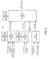
- the interrupt processor 124 may be configured to generate and send interrupts based on the interrupts mechanism or mechanisms enabled by the host 106.
- the interrupt processor 124 may include a ResponseNew counter 280, a last response timer 282, group counters 284 and interrupt send logic 286.
- the ResponseNew counter 280 may be enabled by the host 106 when the watermark interrupt mechanism is desired.
- the host 106 may set the ResponseMark 288, which is a parameter provided as input to the ReponseNew counter 280, as discussed above.
- the ResponseNew counter 280 receives as inputs information including when a response is transferred to the host 106, when the ResponseHead is updated, the number of outstanding responses in the host response buffer 123and when an interrupt has been sent.
- the ResponseNew counter 280 is configured to track the number of responses transferred to the host 106 that the host has yet to see. Each time a response is transferred to the response buffer 123 the counter is incremented.
- the watermark level i.e., the ResponseMark 288, is the number of new responses in the response buffer 123 needed to generate an interrupt. If the host 106 removes new responses from the response buffer 123, they do not count toward meeting the watermark level. When an interrupt is generated, the count toward the ResponseMark is reset.
- the interrupt send logic 286 If the watermark interrupt mechanism is the only interrupt enabled, when the watermark is reached, then the interrupt send logic 286 generates and sends an interrupt to the host 106. No further interrupts will be sent until the host 106 acknowledges the interrupt and updates the ResponseHead. The updated ResponseHead is communicated to the interrupt send logic 286 as a clear interrupt signal. If other interrupt mechanisms also are enabled, then the interrupt send logic 286 may generate and send an interrupt to the host 106 taking into account the other enabled interrupt mechanisms as well.
- the last response timer 282 may be enabled when the timer interrupt mechanism is desired.
- the last response timer 282 may be configured to keep track of time since the last interrupt. For instance, the last response timer 282 may track the amount of time since the last interrupt in microseconds.
- the host 106 may set the amount of time using a parameter, for example, a ResponseDelay parameter 290.
- the ResponseDelay 290 timeout may be the number of microseconds since the last interrupt, or since the last time that the host 106 removed new responses from the response buffer 123, before an interrupt is generated.
- the last response timer 282 receives as input a signal indicating when an interrupt is sent.
- the last response timer 282 also may receive a signal when the ResponseHead is updated, which indicates that the host 106 has removed responses from the response buffer 123.
- An interrupt may be generated only if the response buffer 123 contains outstanding responses.
- the last response timer 282 is configured to generate a timeout trigger when the amount of time being tracked by the last response timer 282 is greater than the ResponseDelay parameter 290. When this occurs and the response buffer 123 contains new responses, then a timeout trigger signal is sent to the interrupt send logic 286. If the last response timer 282 is the only interrupt mechanism enabled, then the interrupt send logic 286 generates and sends an interrupt to the host. If other interrupt mechanisms also are enabled, then the interrupt send logic 286 may take into account the other interrupt mechanisms as well.
- Each interrupt mechanism includes an enable bit and the interrupt send logic 286 may be configured to generate an interrupt when an interrupt trigger is asserted for an enabled interrupt mechanism. The logic may be configure not to generate another interrupt until the host 106 acknowledges the interrupt and updates the ResponseHead.
- the Queue Control parameter 292 may provide input to the interrupt send logic 286 to indicate the status of the interrupt mechanisms such as which of the interrupt mechanisms are enabled and which of the interrupt mechanisms are disabled.
- the group counters 284 mechanism may be arranged and configured to track commands that are part of a group as designated by the driver 107.
- the group counters 284 may be enabled by the host 106 when the host 106 desires to track commands as part of a group such that a single interrupt is generated and sent back to the host 106 only when all of the commands in a group are processed. In this manner, an interrupt is not generated for each of the individual commands but only for the group of commands.
- the group counters 284 may be configured with multiple counters to enable the tracking of multiple different groups of commands.
- the group counters 284 may be configured to track up to and including 128 different groups of commands. In this manner, for each group of commands there is a counter.
- the number of counters may be related to the number of group numbers that may be designated using the interrupt group field in the command header.
- the group counters 284 may be configured to increment the counter for a group when a new command for the group has entered the command processor 122.
- the group counters 284 may decrement the counter for a group when one of the commands in the group has completed processing. In this manner of incrementing as new commands enter for a group and decrementing when commands are completed for the group, the number of commands in each group is potentially unlimited.
- the counters do not need to be sized to account for the largest number of potential commands in a group. Instead, the counters may be sized based on the number of commands that the data storage device 100 may potentially process at one time, which may be smaller than the unlimited number of commands in a particular group.
- each of the group counters 284 may track the commands in a specific group using the group number assigned by the driver 107 and appearing in the interrupt group field in the command header of each command.
- the group counters 284 receive a signal each time a command having a group number enters the command processor 122 for processing. In response to this signal, the counter increments for that group.
- the group counters 284 also receive a signal each time a command having a group number completes processing. In response to this signal, the counter decrements for that group.
- the last command in the command group may be marked by the driver 107 with a flag to indicate to the group counters 284 that the command is the last command in the group.
- the last bit in the interrupt group field in the command header may be used as the flag.
- the group counters 284 are configured to recognize when the flag is set. In this manner, the group counters 284 keep a counter of the number of commands in a particular group that are in processing in the data storage device 100. The group counters 284 also track when the end of the group has been seen.
- the counter for its interrupt group When a command is sent from the host 106 to the data storage device 100, the counter for its interrupt group is incremented. When a response is sent from the data storage device 100 to the host 106, the counter for its interrupt group is decremented. When the last command in the group is received at the groups counters 284 and the count for that group goes to zero, the group trigger signal is generated and sent to the interrupt send logic 286. When the group trigger signal is received at the interrupt send logic 286, then an interrupt is sent to the host 106. The group counters 284 then clear the end group flag for that group.
- the driver 107 may be configured to track the groups in use. The driver 107 may not re-use an interrupt group number until the previous commands to use that interrupt group have all completed and the interrupt has been acknowledged.
- the driver 107 may be configured to determine dynamically how many interrupts it wants to have generated. For example, the driver 107 may dynamically determine the size of a command group depending on various criteria including, for instance, volume, latency and other factors on the host 106.
- the interrupt send logic 286 may be configured to consolidate multiple interrupts for multiple interrupt groups and only send a single interrupt for multiple groups of commands.
- FIG. 3 is a block diagram of a command processor 122.
- the command processor 122 may include a slot tracker module 302, a command transfer module 304, a pending command module 306, a command packet memory 308, and a task dispatch module 310.
- the command processor 122 may be implemented in hardware, software or a combination of hardware and software.
- the command processor 122 may be implemented as a part of a field programmable gate array (FPGA) controller.
- the FPGA controller may be configured using firmware or other instructions to program the FPGA controller to perform the functions discussed herein.
- the command processor 122 may be arranged and configured to retrieve commands from a host and to queue and order the commands from the host for processing by various storage locations.
- the command processor 122 may be configured to maximize the availability of the storage locations by attempting to keep all or substantially all of the storage locations busy.
- the command processor 122 may be configured to dispatch commands designated for the same storage location in order such that the order of the commands received from the host is preserved.
- the command processor 122 may be configured to reorder and dispatch commands designated for different storage locations out of order. In this manner, the commands received from the host may be processed in parallel by reordering the commands designated for different storage locations and, at the same time, the order of the commands designated for the same storage location is preserved.
- the command processor 122 may use an ordered list to queue and order the commands from the host.
- the ordered list may be sorted and/or otherwise ordered based on the age of the commands from the host. For instance, as new commands are received from the host, those commands are placed at the bottom of the ordered list in the order that they were received from the host. In this manner, commands that are dependent on order (e.g., commands designated for the same storage location) are maintained in the correct order.
- the storage locations may include multiple flash memory chips.
- the flash memory chips may be arranged and configured into multiple channels with each of the channels including one or more of the flash memory chips.
- the command processor 122 may be arranged and configured to dispatch commands designated for the same channel and/or the same flash memory chip in order based on the ordered list. Also, the command processor 122 may be arranged and configured to dispatch commands designated for different channels and/or different flash memory chips out of order. In this manner, the command processor 122 may, if needed, reorder the commands from the ordered list so that the channels and the flash memory chips may be kept busy at the same time. This enables the commands from the host to be processed in parallel and enables more commands to be processed at the same time on different channels and different flash memory chips.
- the commands from the host may be dispatched and tracked under the control of a driver (e.g., driver 107 of FIG. 1 ), where the driver may be a computer program product that is tangibly embodied on a storage medium and may include instructions for generating and dispatching commands from the host (e.g., host 106 of FIG. 1 ).
- the commands from the host may designate a specific storage location, for example, a specific flash memory chip and/or a specific channel. From the host perspective, it may be important that commands designated for the same storage location be executed in the order as specified by the host. For example, it may be important that certain operations generated by the host occur in order on a same flash memory chip.
- the host may generate and send an erase command and a write command for a specific flash memory chip, where the host desires that the erase command occurs first. It is important that the erase operation occurs first so that the data associated with the write command doesn't get erased immediately after it is written to the flash memory chip.
- This operation may include multiple commands to perform the operation on the same flash memory chip. In this example, it is necessary to perform these commands for this operation in the order specified by the host. For instance, a single write operation may include more than sixty commands.
- the command processor 122 may be configured to ensure that commands to the same flash memory chip are performed in order using the ordered list.
- the command processor 122 may be configured to track a number of commands being processed.
- the command processor 122 may be configured to track a number of available slots for commands to be received and processed.
- One of the components of the command processor 122, the slot tracker module 302 may be configured to track available slots for commands from the host.
- the slot tracker module 302 may keep track of the open slots, provide the slots to new commands transferred from the host and designate the slots as open upon completion of the commands.
- the slot tracker module 302 may include a fixed number of slots, where each slot may be designated for a single command.
- the slot tracker module 302 may include 128 slots.
- the slot tracker module 302 may include a different number of fixed slots.
- the number of slots may be variable or configurable.
- the slot tracker module 302 may be implemented as a register or memory module in software, hardware or a combination of hardware and software.
- the slot tracker module 302 may include a list of slots, where each of the slots is associated with a global slot identifier. As commands are received from the host, the commands are assigned to an available slot and associated with the global slot identifier for that slot.
- the slot tracker module 302 may be configured to assign each of the commands a global slot identifier, where the number of global slot identifier is fixed to match the number of slots in the slot tracker module 302.
- the command is associated with the global slot identifier throughout its processing until the command is completed and the slot is released.
- the global slot identifier is a tag associated with a particular slot that is assigned to a command that fills that particular slot.
- the tag is associated with the command and remains with the command until processing of the command is complete and the slot it occupied is released and made available to receive a new command.
- the commands may not be placed in order of slots, but instead may be placed in any of the available slots and assigned the global slot identifier associated with that slot.
- one of the components of the command processor 122, the command transfer module 304 may be configured to retrieve new commands from the host based on a number of available slots in the slot tracker module 302 and an availability of new commands at the host.
- the command transfer module 304 may be implemented as a state machine.
- the slot tracker module 302 may provide information to the command transfer module 304 regarding the number of available slots. Also, the command transfer module 304 may query the slot tracker module 302 regarding the number of available slots.
- the command transfer module 304 may use a command tail pointer 312 and a command head pointer 314 to indicate when and how many new commands are available at the host for retrieval.
- the command transfer module 304 may compare the command tail pointer 312 and the command head pointer 314 to determine whether there are commands available for retrieval from the host. If the command tail pointer 312 and the command head pointer 314 are equal, then no commands are available for transfer. If the command tail pointer 312 is greater than the command head pointer 314, then commands are available for transfer.
- the command tail pointer 312 and the command head pointer 314 may be implemented as registers that are configured to hold a pointer value and may be a part of the command processor 122.
- the command tail pointer 314 may be written to by the host.
- the driver may use a memory mapped input/output (MMIO) write to update the command tail pointer 312 when commands are available at the host for retrieval.
- MMIO memory mapped input/output
- the command transfer module 304 updates the command head pointer 314.
- the command transfer module 304 may retrieve some or all of the available commands from the host.
- the command transfer module 304 may retrieve a group of commands in a single access.
- the command transfer module 304 may be configured to retrieve a group of eight commands at a time using a direct memory access (DMA) operation from the host.
- DMA direct memory access
- the command transfer module 304 updates the command head pointer 314.
- the commands may be retrieved from the host through the bus master 316.
- the command transfer module 304 also may write to a host command head pointer (not shown) through the bus master 316 using a DMA operation to update the host command head pointer.
- the queue control 318 may be configured to enable and disable the command transfer module 304.
- the queue control 318 may be implemented as a register that receives instructions from the host through the driver.
- the queue control 318 may be a component of the command processor 122.
- the driver controls the setting of the queue control 318 so that the command transfer module 304 retrieves commands only when the host is ready and has provided the indication that it is ready.
- the queue control 318 register is set to disable, then the command transfer module 104 may not retrieve and process command from the host.
- the retrieved commands are each assigned to one of the available slots by the slot tracker module 302 and associated with the global slot identifier for that available slot.
- the data for the commands may be stored in the command packet memory 308.
- the command packet memory 308 may be implemented as a fixed buffer that is indexed by global slot identifier.
- the data for a particular command may be stored in the command packet memory 308 and indexed by its assigned global slot identifier.
- the data for a particular command may remain in the command packet memory 308 until the command is dispatched to the designated storage location by the task dispatch module 310.
- the command transfer module 304 also may be configured to provide other components of a controller with information related to the commands as indexed by slot. For example, the command transfer module 304 may provide data to a DMA engine. The command transfer module 304 also may provide status packet header data to a status processor. The command transfer module 304 may provide interrupt group data to an interrupt processor. For example, the command transfer module 304 may transfer group information 319 to the interrupt processor (e.g., interrupt processor 124 of FIGS. 1 and 2 ).
- the interrupt processor e.g., interrupt processor 124 of FIGS. 1 and 2 .
- the pending command module 306 may be configured to queue and order the commands using an ordered list that is based on an age of the commands.
- the pending command module 306 may be implemented as a memory module that is configured to store multiple pointers to queue and order the commands.
- the pending command module 306 may include a list of the global slot identifiers for the commands that are pending along with a storage location identifier.
- the storage location identifier may include the designated storage location for where the command is to be processed.
- the storage location identifier may include a channel identifier and/or a flash memory chip identifier.
- the storage location identifier is a part of the command and is assigned by the host through its driver.
- the global slot identifier and storage location information are added to the bottom of the ordered list in the pending command module 306.
- the data for the commands is stored in the command packet memory 308 and indexed by the global slot identifier.
- a pointer to the previous command is included with the command.
- a pointer to the next command is included with the command.
- each item in the ordered list includes a global task identifier, a storage location identifier, a pointer to the previous command and a pointer to the next command.
- the ordered list may be referred to as a doubly linked list.
- the ordered list is a list of the commands ordered from oldest to newest.
- the task dispatch module 310 is configured to remove commands from the ordered list in the pending command module 306 and to dispatch them to the appropriate storage location for processing.
- the task dispatch module 310 may receive input from the storage locations to indicate that they are ready to accept new commands.
- the task dispatch module 310 may receive one or more signals 320 such as signals indicating that one or more of the storage locations are ready to accept new commands.
- the pending command module 306 may be configured to start at the top of the ordered list with the oldest command first and to make that command available to the task dispatch module 310.
- the pending command module 306 may continue to make commands available to the task dispatch module 310 in order using the ordered list until a command is removed from the list by the task dispatch module 310. After a command is removed from the ordered list in the pending command module 306, the pending command module 306 plays back the commands remaining in the list to the task dispatch module 310 starting again at the top of the ordered list.
- the task dispatch module 310 may be configured to start at the top of the ordered list with the oldest command first and determine whether the storage location is available to receive new commands using the signals 320. If the storage location is ready, then the task dispatch module 310 retrieves the command data from the command packet memory 308 and communicates the command data and a storage location select signal 322 to the storage location. The pending command module 306 then updates the ordered list and the pointers to reflect that the command was dispatched for processing. Once a command has been dispatched, the task dispatch module 310 starts at the top of the ordered list again.
- the task dispatch module 310 moves to the next command on the ordered list.
- the task dispatch module 310 determines if the next command is to the same or a different storage location than the skipped command. If the next command is to a same storage location as a skipped command, then the task dispatch module 310 also will skip this command. In this manner, the commands designated for the same storage location are dispatched and processed in order, as received from the host.
- the task dispatch module 310 preserves the order of commands designated for the same storage location. If the commands are designated for a different storage location, the task dispatch module 310 again determines if the storage location for the next command on the list is ready to accept the new command.
- the command is dispatched by the task dispatch module 310 from the command packet memory 308 to the storage location along with a storage location select signal 322.
- the pending command module 306 removes the dispatched command from the ordered list and updates the ordered list including updating the pointers that were associated with the command. In this manner, the remaining pointers are linked together upon removal of the dispatched command.
- the pending command module 306 may include a single memory module 402 having multiple ports, port A and port B.
- the memory module 402 may store information related to the pending commands, including the pointer information for each command, where the pointer information may point to the next command and the previous command.
- the command transfer module 304 of FIG. 3 sends a new entry request 406 for a new command to be added to the ordered list to the pending command module 306.
- the new entry request 406 is received by a new entry module 408.
- the new entry module 408 may be implemented as a state machine.
- the new entry module 408 receives the new entry request 406 and adds it to the ordered list at the end of the list as the newest command in memory module 402. Also, the new entry module 408 requests pointers from the free pointer list module 410.
- the free pointer list module 410 may be implemented as a first-in, first-out (FIFO) memory that maintains a list of pointers that can be used for new entries.
- the free pointer list module 410 provides a next entry pointer 412 to the new entry module 408.
- the next entry pointer 412 is a pointer to where the entry following the current new entry will reside on the ordered list.
- the current new entry in the list points to this address as its next address.
- the new entry pointer 414 is a pointer to where the current new entry will reside on the ordered list, which was the previous entry's next entry pointer 412.
- the last entry in the list points to this address as its next address.
- the memory module 402 stores the data fields related to the commands and the pointers. When a new entry is added, an end pointer 420 also is updated.
- next entry pointer 412 points to the next entry “Y” and the new entry pointer 414 points to the current entry that is to be added, "X”.
- next entry pointer 412 points to the next entry "Z” and the new entry pointer 414 points to the current entry that is to be added, "Y”.
- the task dispatch module 310 of FIG. 3 determines that an entry is to be removed from the ordered list in the memory module 402
- the task dispatch module sends a deletion request 416.
- the deletion request is received by an entry playback and deletion module 418.
- the entry playback and deletion module 418 may be configured to start at the top of the ordered list with the oldest command first and to make that command available to the task dispatch module 310.
- the entry playback and deletion module 418 may continue to make commands available to the task dispatch module 310 in order using the ordered list until a command is removed from the list by the task dispatch module 310.
- the entry playback and deletion module 418 causes the memory module 402 to dispatch the command and remove it from the ordered list.
- the pointers are then freed up and the entry playback and deletion module 418 provides an indication to the free pointer list module 410 that the pointers for the removed command are free.
- the entry playback and deletion module 418 also updates the pointers in the memory module 402 when the command is removed to maintain the correct order of the list.
- the entry playback and deletion module 418 also plays back the commands remaining in the list to the task dispatch module 310 starting again at the top of the ordered list.
- the entry playback and deletion module 418 may be implemented as a state machine.
- the entry playback and deletion module 418 also receives an input of the end pointer 420 from the new entry module 408.
- the end pointer 420 may be used when the entry playback and deletion module 418 is making commands available to the task dispatch module 310 and when a last entry in the ordered list is removed from the list. In this manner, the end pointer 420 may be updated to point to the end of the ordered list.
- the controller board 102 which is its own PCB, may be located physically between each of the memory boards 104a and 104b, which are on their own separate PCBs.
- the data storage device 100 may include the memory board 104a on one PCB, the controller board 102 on a second PCB, and the memory board 104b on a third PCB.
- the memory board 104a includes multiple flash memory chips 118a and the memory board 104b includes multiple flash memory chips 118b.
- the controller board 102 includes the controller 110 and the interface 108 to the host (not shown), as well as other components (not shown).
- the memory board 104a may be operably connected to the controller board 102 and located on one side 520a of the controller board 102.
- the memory board 104a may be connected to a top side 520a of the controller board 102.
- the memory board 104b may be operably connected to the controller board 102 and located on a second side 520b of the controller board 102.
- the memory board 104b may be connected to a bottom side 520b of the controller board 102.
- FIG. 5 merely illustrates one exemplary arrangement.
- the data storage device 100 may include more than two memory board such as three memory boards, four memory boards or more memory boards, where all of the memory boards are connected to a single controller board. In this manner, the data storage device may still be configured in a disk drive form factor.
- the memory boards may be connected to the controller board in other arrangements such as, for instance, the controller board on the top and the memory cards on the bottom or the controller board on the bottom and the memory cards on the top.
- the data storage device 100 may be arranged and configured to cooperate with a computing device.
- the controller board 102 and the memory boards 104a and 104b may be arranged and configured to fit within a drive bay of a computing device.
- FIG. 6 two exemplary computing devices are illustrated, namely a server 630 and a server 640.
- the servers 630 and 640 may be arranged and configured to provide various different types of computing services.
- the servers 630 and 640 may include a host (e.g., host 106 of FIG. 1 ) that includes computer program products having instructions that cause one or more processors in the servers 630 and 640 to provide computing services.
- the type of server may be dependent on one or more application programs (e.g., application(s) 113 of FIG. 1 ) that are operating on the server.
- the servers 630 and 640 may be application servers, web servers, email servers, search servers, streaming media servers, e-commerce servers, file transfer protocol (FTP) servers, other types of servers or combinations of these servers.
- the server 630 may be configured to be a rack-mounted server that operates within a server rack.
- the server 640 may be configured to be a stand-alone server that operates independent of a server rack. Even though the server 640 is not within a server rack, it may be configured to operate with other servers and may be operably connected to other servers.
- Servers 630 and 640 are meant to illustrate example computing devices and other computing devices, including other types of servers, may be used.
- the data storage device 100 of FIGS. 1 and 5 may be sized to fit within a drive bay 635 of the server 630 or the drive bay 645 of the server 640 to provide data storage functionality for the servers 630 and 640.
- the data storage device 100 may be sized to a 3.5" disk drive form factor to fit in the drive bays 635 and 645.
- the data storage device 100 also may be configured to other sizes.
- the data storage device 100 may operably connect and communicate with the servers 630 and 560 using the interface 108. In this manner, the host may communicate commands to the controller board 102 using the interface 108 and the controller 110 may execute the commands using the flash memory chips 118a and 118b on the memory boards 104a and 104b.
- the interface 108 may include a high speed interface between the controller 110 and the host 106.
- the high speed interface may enable for fast transfers of data between the host 106 and the flash memory chips 118a and 118b.
- the high speed interface may include a PCIe interface.
- the PCIe interface may be a PCIe x4 interface or a PCIe x8 interface.
- the PCIe interface 108 may include a connector to the host 106 such as, for example, PCIe connector cable assembly. Other high speed interfaces, connectors and connector assemblies also may be used.
- the communication between the controller board 102 and the flash memory chips 118a and 118b on the memory boards 104a and 104b may be arranged and configured into multiple channels 112.
- Each of the channels 112 may communicate with one or more flash memory chips 118a and 118b and may be controlled by the channel controllers (not shown).
- the controller 110 may be configured such that commands received from the host 106 may be executed by the controller 110 using each of the channels 112 simultaneously or at least substantially simultaneously. In this manner, multiple commands may be executed simultaneously on different channels 112, which may improve throughput of the data storage device 100.
- each of the channels 112 may support multiple flash memory chips.
- each of the channels 112 may support up to 32 flash memory chips.
- each of the 20 channels may be configured to support and communicate with 6 flash memory chips.
- each of the memory boards 104a and 104b would include 60 flash memory chips each.
- the data storage device 100 may be configured to store up to and including multiple terabytes of data.
- the controller 110 may include a microcontroller, a FPGA controller, other types of controllers, or combinations of these controllers.
- the controller 110 is a microcontroller.
- the microcontroller may be implemented in hardware, software, or a combination of hardware and software.
- the microcontroller may be loaded with a computer program product from memory (e.g., memory module 116) including instructions that, when executed, may cause the microcontroller to perform in a certain manner.
- the microcontroller may be configured to receive commands from the host 106 using the interface 108 and to execute the commands.
- the commands may include commands to read, write, copy and erase blocks of data using the flash memory chips 118a and 118b, as well as other commands.
- the controller 110 is a FPGA controller.
- the FPGA controller may be implemented in hardware, software, or a combination of hardware and software.
- the FPGA controller may be loaded with firmware from memory (e.g., memory module 116) including instructions that, when executed, may cause the FPGA controller to perform in a certain manner.
- the FPGA controller may be configured to receive commands from the host 106 using the interface 108 and to execute the commands.
- the commands may include commands to read, write, copy and erase blocks of data using the flash memory chips 118a and 118b, as well as other commands.
- the FPGA controller may support multiple interfaces 108 with the host 106.
- the FPGA controller may be configured to support multiple PCIe x4 or PCIe x8 interfaces with the host 106.
- the memory module 116 may be configured to store data, which may be loaded to the controller 110.
- the memory module 116 may be configured to store one or more images for the FPGA controller, where the images include firmware for use by the FPGA controller.
- the memory module 116 may interface with the host 106 to communicate with the host 106.
- the memory module 116 may interface directly with the host 106 and/or may interface indirectly with the host 106 through the controller 110.
- the host 106 may communicate one or more images of firmware to the memory module 116 for storage.
- the memory module 116 includes an electrically erasable programmable read-only memory (EEPROM).
- EEPROM electrically erasable programmable read-only memory
- the memory module 116 also may include other types of memory modules.
- the power module 114 may be configured to receive power (Vin), to perform any conversions of the received power and to output an output power (Vout).
- the power module 114 may receive power (Vin) from the host 106 or from another source.
- the power module 114 may provide power (Vout) to the controller board 102 and the components on the controller board 102, including the controller 110.
- the power module 114 also may provide power (Vout) to the memory boards 104a and 104b and the components on the memory boards 104a and 104b, including the flash memory chips 118a and 118b.
- the power module 114 may include one or more direct current (DC) to DC converters.
- the DC to DC converters may be configured to receive a power in (Vin) and to convert the power to one or more different voltage levels (Vout).
- Vin power in
- Vout voltage levels
- the power module 114 may be configured to receive +12 V (Vin) and to convert the power to 3.3v, 1.2v, or 1.8v and to supply the power out (Vout) to the controller board 102 and to the memory boards 104a and 104b.
- the memory boards 104a and 104b may be configured to handle different types of flash memory chips 118a and 118b.
- the flash memory chips 118a and the flash memory chips 118b may be the same type of flash memory chips including requiring the same voltage from the power module 114 and being from the same flash memory chip vendor.
- vendor and manufacturer are used interchangeably throughout this document.
- the flash memory chips 118a on the memory board 104a may be a different type of flash memory chip from the flash memory chips 118b on the memory board 104b.
- the memory board 104a may include SLC NAND flash memory chips and the memory board 104b may include MLC NAND flash memory chips.
- the memory board 104a may include flash memory chips from one flash memory chip manufacturer and the memory board 104b may include flash memory chips from a different flash memory chip manufacturer. The flexibility to have all the same type of flash memory chips or to have different types of flash memory chips enables the data storage device 100 to be tailored to different application(s) 113 being used by the host 106.
- the memory boards 104a and 104b may include different types of flash memory chips on the same memory board.
- the memory board 104a may include both SLC NAND chips and MLC NAND chips on the same PCB.
- the memory board 104b may include both SLC NAND chips and MLC NAND chips. In this manner, the data storage device 100 may be advantageously tailored to meet the specifications of the host 106.
- the memory boards 104a and 104b may include other types of memory devices, including non-flash memory chips.
- the memory boards 104a and 104b may include random access memory (RAM) such as, for instance, dynamic RAM (DRAM) and static RAM (SRAM) as well as other types of RAM and other types of memory devices.
- RAM random access memory
- DRAM dynamic RAM
- SRAM static RAM
- the both of the memory boards 104a and 104b may include RAM.
- one of the memory boards may include RAM and the other memory board may include flash memory chips.
- one of the memory boards may include both RAM and flash memory chips.
- the memory modules 120a and 120b on the memory boards 104a and 104b may be used to store information related to the flash memory chips 118a and 118b, respectively.
- the memory modules 120a and 120b may store device characteristics of the flash memory chips. The device characteristics may include whether the chips are SLC chips or MLC chips, whether the chips are NAND or NOR chips, a number of chip selects, a number of blocks, a number of pages per block, a number of bytes per page and a speed of the chips.
- the memory modules 120a and 120b may include serial EEPROMs.
- the EEPROMs may store the device characteristics.
- the device characteristics may be compiled once for any given type of flash memory chip and the appropriate EEPROM image may be generated with the device characteristics.
- the controller board 102 When the memory boards 104a and 104b are operably connected to the controller board 102, then the device characteristics may be read from the EEPROMs such that the controller 110 may automatically recognize the types of flash memory chips 118a and 118b that the controller 110 is controlling. Additionally, the device characteristics may be used to configure the controller 110 to the appropriate parameters for the specific type or types of flash memory chips 118a and 118b.
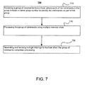
- Process 700 may include receiving a group of commands from a host, where each of the commands in the group includes a same group number to identify the commands as part of the group (710), processing the group of commands using multiple memory chips (720) and generating and sending a single interrupt to the host when the group of commands completes processing (703).
- the controller 110 may be configured to perform the process 700.
- the controller 110 and its components may be configured to receive a group of commands from the host 106, where the host 106 assigns a same group number in the command header of each of the commands in the groups to identify the commands as part of the group (710).
- the command processor 122 may be configured to process the commands using the flash memory chips 118a and 118b (720).
- the command processor 122 may be configured to process the commands in a non-contiguous order using the flash memory chips 118a and 118b.
- the interrupt processor 124 may be configured to generate and send the single interrupt when the group of commands completes processing (730).
- the controller 110 may be configured to receive multiple groups of commands from the host 106, where each of the different groups of commands is assigned a different group number.
- the driver 107 may be configured to track the group numbers that are assigned to the different groups of commands.
- the command processor 122 may be configured to process the multiple groups of commands.
- the interrupt processor 124 may be configured to generate and send a single interrupt for each of the different groups of commands when all of the commands in a particular group complete processing.
- Process 800 may include incrementing a group counter when a command in a group of commands begins processing (810), decrementing the group counter when a command in the group of commands completes processing (820) and generating and sending a single interrupt for the group of commands when all of the commands in the complete processing (830).
- process 800 may be performed by the controller 110 and its components.
- the interrupt processor 124 may be configured to increment a group counter 284 when a command in the group of commands begins processing (810).
- the interrupt processor 124 may be configured to decrement the group counter 284 when a command in the group of commands completes processing (820).
- the interrupt processor 124 may be configured to generate and send the single interrupt for the group of commands when all of the commands in the group complete processing (830).
- the interrupt processor 124 may generate and send the single interrupt command when a last command in the group of commands begins processing and the group counter is decremented to zero.
- Implementations of the various techniques described herein may be implemented in digital electronic circuitry, or in computer hardware, firmware, software, or in combinations of them. Implementations may be implemented as a computer program product, i.e., a computer program tangibly embodied in an information carrier, e.g., in a machine-readable storage device, for execution by, or to control the operation of, data processing apparatus, e.g., a programmable processor, a computer, or multiple computers.
- a computer program such as the computer program(s) described above, can be written in any form of programming language, including compiled or interpreted languages, and can be deployed in any form, including as a stand-alone program or as a module, component, subroutine, or other unit suitable for use in a computing environment.
- a computer program can be deployed to be executed on one computer or on multiple computers at one site or distributed across multiple sites and interconnected by a communication network.
- Method steps may be performed by one or more programmable processors executing a computer program to perform functions by operating on input data and generating output. Method steps also may be performed by, and an apparatus may be implemented as, special purpose logic circuitry, e.g., a FPGA (field programmable gate array) or an ASIC (application-specific integrated circuit).
- a FPGA field programmable gate array
- ASIC application-specific integrated circuit
- processors suitable for the execution of a computer program include, by way of example, both general and special purpose microprocessors, and any one or more processors of any kind of digital computer.
- a processor will receive instructions and data from a read-only memory or a random access memory or both.
- Elements of a computer may include at least one processor for executing instructions and one or more memory devices for storing instructions and data.
- a computer also may include, or be operatively coupled to receive data from or transfer data to, or both, one or more mass storage devices for storing data, e.g., magnetic, magneto-optical disks, or optical disks.
- Information carriers suitable for embodying computer program instructions and data include all forms of non-volatile memory, including by way of example semiconductor memory devices, e.g., EPROM, EEPROM, and flash memory devices; magnetic disks, e.g., internal hard disks or removable disks; magneto-optical disks; and CD-ROM and DVD-ROM disks.
- semiconductor memory devices e.g., EPROM, EEPROM, and flash memory devices
- magnetic disks e.g., internal hard disks or removable disks
- magneto-optical disks e.g., CD-ROM and DVD-ROM disks.
- the processor and the memory may be supplemented by, or incorporated in special purpose logic circuitry.
- implementations may be implemented on a computer having a display device, e.g., a cathode ray tube (CRT) or liquid crystal display (LCD) monitor, for displaying information to the user and a keyboard and a pointing device, e.g., a mouse or a trackball, by which the user can provide input to the computer.
- a display device e.g., a cathode ray tube (CRT) or liquid crystal display (LCD) monitor
- keyboard and a pointing device e.g., a mouse or a trackball
- Other kinds of devices can be used to provide for interaction with a user as well; for example, feedback provided to the user can be any form of sensory feedback, e.g., visual feedback, auditory feedback, or tactile feedback; and input from the user can be received in any form, including acoustic, speech, or tactile input.
- Implementations may be implemented in a computing system that includes a back-end component, e.g., as a data server, or that includes a middleware component, e.g., an application server, or that includes a front-end component, e.g., a client computer having a graphical user interface or a Web browser through which a user can interact with an implementation, or any combination of such back-end, middleware, or front-end components.
- Components may be interconnected by any form or medium of digital data communication, e.g., a communication network. Examples of communication networks include a local area network (LAN) and a wide area network (WAN), e.g., the Internet.
- LAN local area network
- WAN wide area network
Landscapes
- Engineering & Computer Science (AREA)
- Theoretical Computer Science (AREA)
- Physics & Mathematics (AREA)
- General Engineering & Computer Science (AREA)
- General Physics & Mathematics (AREA)
- Human Computer Interaction (AREA)
- Computer Security & Cryptography (AREA)
- Techniques For Improving Reliability Of Storages (AREA)
- Bus Control (AREA)
- Information Retrieval, Db Structures And Fs Structures Therefor (AREA)
- Information Transfer Systems (AREA)
- Image Processing (AREA)
- Memory System Of A Hierarchy Structure (AREA)
Description
- This description relates to command and interrupt grouping for a data storage device.
- Data storage devices may be used to store data. A data storage device may be used with a computing device to provide for the data storage needs of the computing device. In certain instances, it may be desirable to store large amounts of data on a data storage device. Also, it may be desirable to execute commands quickly to read data and to write data to the data storage device.
- The throughput of the command execution on the data storage device may be related to the number of commands that may be processed by the data storage device. It may be desirable to achieve a high throughput for the data storage device by increasing the number of commands that may be processed by the data storage device. In addition to executing the commands quickly, it may be desirable to execute the commands accurately, such that data errors are minimized and/or the data errors are correctible with at least a minimal impact on data throughput.
- Furthermore, it may be desirable to execute commands received from a host on the data storage device while minimizing the impact and overhead on the host.
-
US 5,802,345 refers to an auxiliary memory unit with hard disc drives or - alternatively - with semiconductor storage devices, as well as a memory processing unit (MPU). A CPU of a host machine generates commands to access the auxiliary memory unit and groups these commands. The MPU of the memory unit notifies the CPU by a single interruption that execution of the commands of the group has been terminated. - This document describes a host having a driver that designates commands as part of a group for processing by a data storage device. When the data storage device completes the processing of all of the commands in the group, the data storage device sends a single interrupt back to the host to indicate that the processing of the group of commands is complete. For example, one or more threads of commands may be designated as a group by the driver. When the data storage device completes the thread or threads of commands, the data storage device generates and sends a single interrupt to the host to indicate that the processing of those grouped commands is complete.
- By designating the commands as part of a group and sending a single interrupt to the host when the processing of the commands is complete, the impact on the host may be minimized. In this manner, the host may spend less time processing interrupts and may devote more time performing other tasks. Moreover, in some instances, the host may not be able to use any of the data until all of the commands in the group have been processed. In those instances, it may not be useful for the host be notified when less than all of the commands in the group have been processed.
- One aspect of the present invention is a data storage device as defined in independent claim 1. Another aspect of the invention is a method as defined in independent claim 15. Further embodiments of the invention are specified in the respective appended dependent claims.
- The details of one or more implementations are set forth in the accompanying drawings and the description below. Other features will be apparent from the description and drawings, and from the claims.
-
-
FIG. 1 is an exemplary block diagram of a host and a data storage device. -
FIG. 2 is an exemplary block diagram of an interrupt processor. -
FIG. 3 is an exemplary block diagram of a command processor for the data storage device. -
FIG. 4 is an exemplary block diagram of a pending command module. -
FIG. 5 is an exemplary perspective block diagram of the printed circuit boards of the data storage device. -
FIG. 6 is an exemplary block diagram of exemplary computing devices for use with the data storage device ofFIG. 1 . -
FIG. 7 is an exemplary flowchart illustrating a process for processing a group of commands on a data storage device. -
FIG. 8 is an exemplary flowchart illustrating a process for tracking commands in a controller. - This document describes an apparatus, system(s) and techniques for grouping commands at a host and processing the commands in a data storage device. The host may determine which commands to group together and may provide an indication of which commands are in a same group. For example, the host may assign and insert a group number into the command header of each command that is part of a group. The data storage device may include a controller having an interrupt processor that is configured to track the processing of the commands, which have been grouped together by the host. When the data storage device completes the processing of all of the commands in the group, the interrupt processor generates and sends a single interrupt back to the host to indicate that the processing of the group of commands is complete.
- Referring to
FIG. 1 , a block diagram of a system for processing and tracking commands in a group is illustrated.FIG. 1 illustrates a block diagram of adata storage device 100 and ahost 106. Thedata storage device 100 may include acontroller board 102 and one ormore memory boards data storage device 100 may communicate with thehost 106 over aninterface 108. Theinterface 108 may be between thehost 106 and thecontroller board 102. - The
controller board 102 may include acontroller 110, aDRAM 111,multiple channels 112, apower module 114, and amemory module 116. Thecontroller 110 may include acommand processor 122 and aninterrupt processor 124, as well as other components, which are not shown. Thememory boards flash memory chips memory boards memory device - The
host 106 may include adriver 107, anoperating system 109 and one ormore applications 113. In general, thehost 106 may generate commands to be executed on thedata storage device 100. For example, theapplication 113 may be configured to generate commands for execution on thedata storage device 100. Theapplication 113 may be operably coupled to theoperating system 109 and/or to thedriver 107. Theapplication 113 may generate the commands and communicate the commands to theoperating system 109. Theoperating system 109 may be operably coupled to thedriver 107, where thedriver 107 may act as an interface between thehost 106 and thedata storage device 100. - In general, the
data storage device 100 may be configured to store data on theflash memory chips host 106 may write data to and read data from theflash memory chips flash memory chips host 106 and theflash memory chips controller 110 on thecontroller board 102. Thecontroller 110 may receive commands from thehost 106 and cause those commands to be executed using thecommand processor 122 and theflash memory chips memory boards host 106 and thecontroller 110 may be through theinterface 108. Thecontroller 110 may communicate with theflash memory chips channels 112. - The
controller board 102 may includeDRAM 111. TheDRAM 111 may be operably coupled to thecontroller 110 and may be used to store information. For example, theDRAM 111 may be used to store logical address to physical address maps and bad block information. TheDRAM 111 also may be configured to function as a buffer between thehost 106 and theflash memory chips - In one exemplary implementation, the
controller board 102 and each of thememory boards memory board 104a may be on one PCB that is operably connected to thecontroller board 102 PCB. For example, thememory board 104a may be physically and/or electrically connected to thecontroller board 102. Similarly, thememory board 104b may be a separate PCB from thememory board 104a and may be operably connected to thecontroller board 102 PCB. For example, thememory board 104b may be physically and/or electrically connected to thecontroller board 102. Thememory boards controller board 102. For example, thememory board 104a may be disconnected from thecontroller board 102 and replaced with another memory board (not shown), where the other memory board is operably connected tocontroller board 102. In this example, either or both of thememory boards same controller board 102 andcontroller 110. - In one exemplary implementation, the
controller board 102 and each of thememory boards - In one exemplary implementation, the
controller board 102 and each of thememory boards - In one exemplary implementation, the
memory chips 118a-118n may include flash memory chips. In another exemplary implementation, thememory chips 118a-118n may include DRAM chips or combinations of flash memory chips and DRAM chips. Thememory chips 118a-118n may include other types of memory chips as well. - In one exemplary implementation, the
host 106 using thedriver 107 and thedata storage device 100 may communicate commands and responses using pairs of buffers in host memory. The terms "buffer" and "queue" are used interchangeably throughout this document. For example, acommand buffer 119 may be used for commands and aresponse buffer 123 may be used for responses or results to the commands. In one exemplary implementation, the commands and results may be relatively small, fixed size blocks. For instance, the commands may be 32 bytes and the results or responses may be 8 bytes. In other exemplary implementations, other sized blocks may be used including variable size blocks. Tags may be used to match the results to the commands. In this manner, thedata storage device 100 may complete commands out of order. - Although
FIG. 1 illustrates onecommand buffer 119 and oneresponse buffer 123, multiple pairs of buffers may be used. For example, up to and including 32 buffer pairs may be used. In one exemplary implementation, thedata storage device 100 may service thecommand buffer 119 in a round robin fashion, where thedata storage device 100 may retrieve a fixed number of commands at a time from thecommand buffer 119. Theresponse buffer 123 may include its own interrupt and interrupt parameters. - In one exemplary implementation, each command may refer to one memory page (e.g., one flash page), one erase block or one memory chip depending on the command. Each command that transfers data may include one 4K direct memory access (DMA) buffer. Larger operations may be implemented by sending multiple commands. The
driver 107 may be arranged and configured group together a single operation of multiple commands such that thedata storage device 100 processes the commands using theflash memory chips host 106 when the multiple grouped commands have been processed. - In one exemplary implementation, the
command buffer 119 and theresponse buffer 123 each include a head pointer and a tail pointer. Commands and responses may be inserted at the tail pointer and removed at the head pointer. Thehost 106 may be the producer of thecommand buffer 119 and the consumer of theresponse buffer 123. Thedata storage device 100 may be the consumer of thecommand buffer 119 and the producer of theresponse buffer 123. Thehost 106 may write the command tail pointer and the response head pointer and may read the command head pointer and the response tail pointer. Thedata storage device 100 may write the command head pointer and the response tail pointer and may read the command tail pointer and the response head pointer. In thedata storage device 100, thecontroller 110 may perform the read and write actions. More specifically, thecommand processor 122 may be configured to perform the read and write actions for thedata storage device 100. No other synchronization, other than the head and tail pointers, may be needed between thehost 106 and thedata storage device 100. - In one exemplary implementation, for performance reasons, the command head pointer and the response tail pointer may be stored in the host 106 (e.g., in host RAM). The command tail pointer and the response head pointer may be stored in the
data storage device 100 in memory mapped I/O space within thecontroller 110. - The
command buffer 119 and theresponse buffer 123 may be an arbitrary multiple of the command or response sizes, and thedriver 107 and thedata storage device 100 may be free to post and process commands and results as needed provided that they do not overrun thecommand buffer 119 and theresponse buffer 123. In one implementation, thecommand buffer 119 and theresponse buffer 123 are circular buffers, which enable flow control between thehost 106 and thedata storage device 100. - In one exemplary implementation, the
host 106 may determine the size of thecommand buffer 119 and theresponse buffer 123. The buffers may be larger than the number of commands that thedata storage device 100 can queue internally. - The
host 106 may write a command to thecommand buffer 119 and update the command tail pointer to indicate to thedata storage device 100, and thecommand processor 122 within thedata storage device 100, that a new command is present. The write of the command tail pointer signals thecommand processor 122 that a new command is present. Thecommand processor 122 is configured to read the command from thecommand buffer 119 using a DMA operation and is configured to update the head pointer using another DMA operation to indicate to thehost 106 that thecommand processor 122 has received the command. - When the
command processor 122 completes the command, thecommand processor 122 writes the response using a DMA operation and updates the response tail pointer with another DMA operation to indicate that the command is finished. The interruptprocessor 124 is configured to signal thehost 106 with an interrupt when new responses are available in theresponse buffer 123. Thehost 106 is configured to read the responses from theresponse buffer 123 and update the head pointer to indicate that it has received the response. In one exemplary implementation, the interruptprocessor 124 may not send another interrupt to thehost 106 until the previous interrupt has been acknowledged by thehost 106 writing to the response head pointer. - In one exemplary implementation, the
host 106, through itsdriver 107, may control when the interruptprocessor 124 should generate interrupts. Thehost 106 may use one or more different interrupt mechanisms, including a combination of different interrupt mechanisms, to provide information to the interruptprocessor 124 regarding interrupt processing. For instance, thehost 106 through thedriver 107 may configure the interruptprocessor 124 to use a water mark interrupt mechanism, a timeout interrupt mechanism, a group interrupt mechanism, or a combination of these interrupt mechanisms. - In one exemplary implementation, the
host 106 may set a ResponseMark parameter, which determines the water mark, and may set the ResponseDelay parameter, which determines the timeout. Thehost 106 may communicate these parameters to the interruptprocessor 124. If the count of new responses in theresponse buffer 123 is equal to or greater than the ResponseMark, then an interrupt is generated by the interruptprocessor 124 and the count is zeroed. If the time (e.g., time in microseconds) since the last interrupt is equal to or greater than the ResponseDelay and there are new responses in theresponse buffer 123, then the interruptprocessor 124 generates an interrupt and the timeout is zeroed. If thehost 106 removes the new response from theresponse buffer 123, the count of new responses is updated and the timeout is restarted. In this manner, thehost 106 may poll ahead and avoid interrupts from the interruptprocessor 124. - In another exemplary implementation, the
host 106 may use a group interrupt mechanism to determine when the interruptprocessor 124 should generate and send interrupts to thehost 106. The commands may share a common value, which identifies the commands as part of the same group. For example, thedriver 107 may group commands together and assign a same group number to the group of commands. Thedriver 107 may use an interrupt group field in the command header to assign a group number to the commands in a group. When all of the commands in a command group have completed, and the responses for all of those commands have been transferred from thecommand processor 122 to theresponse buffer 123 and the response tail is updated, then the interruptprocessor 124 may generate and send the interrupt to thehost 106. In this manner, the group interrupt mechanism may be used to reduce the time thehost 106 needs to spend processing interrupts. - Each of the interrupt mechanisms may be separately enabled or disabled. Also, any combination of interrupt mechanisms may be used. For example, the
driver 107 may set interrupt enable and disable flags in a QueueControl register to determine which of the interrupt mechanisms are enabled and which of the interrupt mechanisms are disabled. In this manner, the combination of the interrupts may be used to reduce the time that thehost 106 needs to spend processing interrupts. Thehost 106 may use its resources to perform other tasks. - In one exemplary implementation, all of the interrupt mechanisms may be disabled. In this situation, the
driver 107 may be configured to poll theresponse buffer 123 to determine if there are responses ready for processing. Having all of the interrupt mechanisms disabled may result in a lowest possible latency. It also may result in a high overhead for thedriver 107. - In another exemplary implementation, the group interrupt mechanism may be enabled along with the timeout interrupt mechanism and/or the water mark interrupt mechanism. In this manner, if the number of commands in a designated group is larger than the
response buffer 123, one of the other enabled interrupt mechanisms will function to interrupt thedriver 107 to clear the responses from theresponse buffer 123 to provide space for thecommand processor 122 to add more responses to theresponse buffer 123. - The use of the different interrupt mechanisms, either alone or in combinations, may be used to adjust the latency and/or the overhead with respect to the
driver 107. For example, in one exemplary implementation, only the timeout interrupt mechanism may be enabled. In this situation, the overhead on thedriver 107 may be reduced. In another exemplary implementation, only the water mark interrupt mechanism may be enabled. In this situation, the latency may be reduced to a lower level. - In some exemplary situations, a particular type of application being used may factor into the determination of which interrupt mechanisms are enabled. For example, a web search application may be latency sensitive and may the interrupt mechanisms may be enabled in particular combinations to provide the best latency sensitivity for the web search application. In another example, a web indexing application may not be as sensitive to latency as a web search application. Instead, processor performance may be a more important parameter. In this application, the interrupt mechanisms may be enabled in particular combinations to allow low overhead, even at the expense of increased latency.
- In one exemplary implementation, the
driver 107 may determine a command group based on an input/output (I/O) operation received from anapplication 113 through theoperating system 109. For example, theapplication 113 may request a read operation of multiple megabytes. In this instance, theapplication 113 may not be able to use partial responses and the only useful information for theapplication 113 may be when the entire operation has been completed. Typically, the read operation may be broken up into many multiple commands. Thedriver 107 may be configured to recognize the read operation as a group of commands and to assign the commands in that group the same group number in each of the command headers. An interface between theapplication 113 and thedriver 107 may be used to indicate to thedriver 107 that certain operations are to be treated as a group. The interface may be configured to group operations based on different criteria including, but not limited to, the type of command, the size of the data request associated with the command, the type of data requested including requests from multiple different applications, the priority of the request, and combinations thereof. - In some implementations, the
application 113 may pass individual command information relating to an operation to theoperating system 109 and ultimately to thedriver 107. In other exemplary implementations, thedriver 107 may designate one or more threads of commands to be considered a group. - Referring to
FIG. 2 , a block diagram of an exemplary interruptprocessor 124 is illustrated. The interruptprocessor 124 may be configured to generate and send interrupts based on the interrupts mechanism or mechanisms enabled by thehost 106. The interruptprocessor 124 may include aResponseNew counter 280, alast response timer 282, group counters 284 and interruptsend logic 286. - The
ResponseNew counter 280 may be enabled by thehost 106 when the watermark interrupt mechanism is desired. Thehost 106 may set theResponseMark 288, which is a parameter provided as input to theReponseNew counter 280, as discussed above. TheResponseNew counter 280 receives as inputs information including when a response is transferred to thehost 106, when the ResponseHead is updated, the number of outstanding responses in the host response buffer 123and when an interrupt has been sent. TheResponseNew counter 280 is configured to track the number of responses transferred to thehost 106 that the host has yet to see. Each time a response is transferred to theresponse buffer 123 the counter is incremented. When thecounter 280 reaches or exceed the watermark level set by thehost 106, i.e., theResponseMark 288, then a watermark trigger is generated and sent to the interruptsend logic 286. The watermark level, i.e., theResponseMark 288, is the number of new responses in theresponse buffer 123 needed to generate an interrupt. If thehost 106 removes new responses from theresponse buffer 123, they do not count toward meeting the watermark level. When an interrupt is generated, the count toward the ResponseMark is reset. - If the watermark interrupt mechanism is the only interrupt enabled, when the watermark is reached, then the interrupt
send logic 286 generates and sends an interrupt to thehost 106. No further interrupts will be sent until thehost 106 acknowledges the interrupt and updates the ResponseHead. The updated ResponseHead is communicated to the interruptsend logic 286 as a clear interrupt signal. If other interrupt mechanisms also are enabled, then the interruptsend logic 286 may generate and send an interrupt to thehost 106 taking into account the other enabled interrupt mechanisms as well. - The
last response timer 282 may be enabled when the timer interrupt mechanism is desired. Thelast response timer 282 may be configured to keep track of time since the last interrupt. For instance, thelast response timer 282 may track the amount of time since the last interrupt in microseconds. Thehost 106 may set the amount of time using a parameter, for example, aResponseDelay parameter 290. In one exemplary implementation, theResponseDelay 290 timeout may be the number of microseconds since the last interrupt, or since the last time that thehost 106 removed new responses from theresponse buffer 123, before an interrupt is generated. - The
last response timer 282 receives as input a signal indicating when an interrupt is sent. Thelast response timer 282 also may receive a signal when the ResponseHead is updated, which indicates that thehost 106 has removed responses from theresponse buffer 123. An interrupt may be generated only if theresponse buffer 123 contains outstanding responses. - The
last response timer 282 is configured to generate a timeout trigger when the amount of time being tracked by thelast response timer 282 is greater than theResponseDelay parameter 290. When this occurs and theresponse buffer 123 contains new responses, then a timeout trigger signal is sent to the interruptsend logic 286. If thelast response timer 282 is the only interrupt mechanism enabled, then the interruptsend logic 286 generates and sends an interrupt to the host. If other interrupt mechanisms also are enabled, then the interruptsend logic 286 may take into account the other interrupt mechanisms as well. - Each interrupt mechanism includes an enable bit and the interrupt
send logic 286 may be configured to generate an interrupt when an interrupt trigger is asserted for an enabled interrupt mechanism. The logic may be configure not to generate another interrupt until thehost 106 acknowledges the interrupt and updates the ResponseHead. TheQueue Control parameter 292 may provide input to the interruptsend logic 286 to indicate the status of the interrupt mechanisms such as which of the interrupt mechanisms are enabled and which of the interrupt mechanisms are disabled. - The group counters 284 mechanism may be arranged and configured to track commands that are part of a group as designated by the
driver 107. The group counters 284 may be enabled by thehost 106 when thehost 106 desires to track commands as part of a group such that a single interrupt is generated and sent back to thehost 106 only when all of the commands in a group are processed. In this manner, an interrupt is not generated for each of the individual commands but only for the group of commands. - The group counters 284 may be configured with multiple counters to enable the tracking of multiple different groups of commands. In one exemplary implementation, the group counters 284 may be configured to track up to and including 128 different groups of commands. In this manner, for each group of commands there is a counter. The number of counters may be related to the number of group numbers that may be designated using the interrupt group field in the command header.
- The group counters 284 may be configured to increment the counter for a group when a new command for the group has entered the
command processor 122. The group counters 284 may decrement the counter for a group when one of the commands in the group has completed processing. In this manner of incrementing as new commands enter for a group and decrementing when commands are completed for the group, the number of commands in each group is potentially unlimited. The counters do not need to be sized to account for the largest number of potential commands in a group. Instead, the counters may be sized based on the number of commands that thedata storage device 100 may potentially process at one time, which may be smaller than the unlimited number of commands in a particular group. - In one exemplary implementation, each of the group counters 284 may track the commands in a specific group using the group number assigned by the
driver 107 and appearing in the interrupt group field in the command header of each command. The group counters 284 receive a signal each time a command having a group number enters thecommand processor 122 for processing. In response to this signal, the counter increments for that group. The group counters 284 also receive a signal each time a command having a group number completes processing. In response to this signal, the counter decrements for that group. - The last command in the command group may be marked by the
driver 107 with a flag to indicate to the group counters 284 that the command is the last command in the group. In one exemplary implementation, the last bit in the interrupt group field in the command header may be used as the flag. The group counters 284 are configured to recognize when the flag is set. In this manner, the group counters 284 keep a counter of the number of commands in a particular group that are in processing in thedata storage device 100. The group counters 284 also track when the end of the group has been seen. - When a command is sent from the
host 106 to thedata storage device 100, the counter for its interrupt group is incremented. When a response is sent from thedata storage device 100 to thehost 106, the counter for its interrupt group is decremented. When the last command in the group is received at the groups counters 284 and the count for that group goes to zero, the group trigger signal is generated and sent to the interruptsend logic 286. When the group trigger signal is received at the interruptsend logic 286, then an interrupt is sent to thehost 106. The group counters 284 then clear the end group flag for that group. - The
driver 107 may be configured to track the groups in use. Thedriver 107 may not re-use an interrupt group number until the previous commands to use that interrupt group have all completed and the interrupt has been acknowledged. - In one exemplary implementation, the
driver 107 may be configured to determine dynamically how many interrupts it wants to have generated. For example, thedriver 107 may dynamically determine the size of a command group depending on various criteria including, for instance, volume, latency and other factors on thehost 106. - In one exemplary implementation, the interrupt
send logic 286 may be configured to consolidate multiple interrupts for multiple interrupt groups and only send a single interrupt for multiple groups of commands. -
FIG. 3 is a block diagram of acommand processor 122. Thecommand processor 122 may include aslot tracker module 302, acommand transfer module 304, a pendingcommand module 306, acommand packet memory 308, and atask dispatch module 310. Thecommand processor 122 may be implemented in hardware, software or a combination of hardware and software. In one exemplary implementation, thecommand processor 122 may be implemented as a part of a field programmable gate array (FPGA) controller. The FPGA controller may be configured using firmware or other instructions to program the FPGA controller to perform the functions discussed herein. - The
command processor 122 may be arranged and configured to retrieve commands from a host and to queue and order the commands from the host for processing by various storage locations. Thecommand processor 122 may be configured to maximize the availability of the storage locations by attempting to keep all or substantially all of the storage locations busy. Thecommand processor 122 may be configured to dispatch commands designated for the same storage location in order such that the order of the commands received from the host is preserved. Thecommand processor 122 may be configured to reorder and dispatch commands designated for different storage locations out of order. In this manner, the commands received from the host may be processed in parallel by reordering the commands designated for different storage locations and, at the same time, the order of the commands designated for the same storage location is preserved. - In one exemplary implementation, the
command processor 122 may use an ordered list to queue and order the commands from the host. In one exemplary implementation, the ordered list may be sorted and/or otherwise ordered based on the age of the commands from the host. For instance, as new commands are received from the host, those commands are placed at the bottom of the ordered list in the order that they were received from the host. In this manner, commands that are dependent on order (e.g., commands designated for the same storage location) are maintained in the correct order. - In one exemplary implementation, the storage locations may include multiple flash memory chips. The flash memory chips may be arranged and configured into multiple channels with each of the channels including one or more of the flash memory chips. The
command processor 122 may be arranged and configured to dispatch commands designated for the same channel and/or the same flash memory chip in order based on the ordered list. Also, thecommand processor 122 may be arranged and configured to dispatch commands designated for different channels and/or different flash memory chips out of order. In this manner, thecommand processor 122 may, if needed, reorder the commands from the ordered list so that the channels and the flash memory chips may be kept busy at the same time. This enables the commands from the host to be processed in parallel and enables more commands to be processed at the same time on different channels and different flash memory chips. - The commands from the host may be dispatched and tracked under the control of a driver (e.g.,
driver 107 ofFIG. 1 ), where the driver may be a computer program product that is tangibly embodied on a storage medium and may include instructions for generating and dispatching commands from the host (e.g., host 106 ofFIG. 1 ). The commands from the host may designate a specific storage location, for example, a specific flash memory chip and/or a specific channel. From the host perspective, it may be important that commands designated for the same storage location be executed in the order as specified by the host. For example, it may be important that certain operations generated by the host occur in order on a same flash memory chip. For example, the host may generate and send an erase command and a write command for a specific flash memory chip, where the host desires that the erase command occurs first. It is important that the erase operation occurs first so that the data associated with the write command doesn't get erased immediately after it is written to the flash memory chip. - As another example, for flash memory chips, it may be important to write to pages of an erase block in order. This operation may include multiple commands to perform the operation on the same flash memory chip. In this example, it is necessary to perform these commands for this operation in the order specified by the host. For instance, a single write operation may include more than sixty commands. The
command processor 122 may be configured to ensure that commands to the same flash memory chip are performed in order using the ordered list. - In one exemplary implementation, the
command processor 122 may be configured to track a number of commands being processed. Thecommand processor 122 may be configured to track a number of available slots for commands to be received and processed. One of the components of thecommand processor 122, theslot tracker module 302, may be configured to track available slots for commands from the host. Theslot tracker module 302 may keep track of the open slots, provide the slots to new commands transferred from the host and designate the slots as open upon completion of the commands. - In one exemplary implementation, the
slot tracker module 302 may include a fixed number of slots, where each slot may be designated for a single command. For example, theslot tracker module 302 may include 128 slots. In other exemplary implementations, theslot tracker module 302 may include a different number of fixed slots. Also, for example, the number of slots may be variable or configurable. Theslot tracker module 302 may be implemented as a register or memory module in software, hardware or a combination of hardware and software. - The
slot tracker module 302 may include a list of slots, where each of the slots is associated with a global slot identifier. As commands are received from the host, the commands are assigned to an available slot and associated with the global slot identifier for that slot. Theslot tracker module 302 may be configured to assign each of the commands a global slot identifier, where the number of global slot identifier is fixed to match the number of slots in theslot tracker module 302. The command is associated with the global slot identifier throughout its processing until the command is completed and the slot is released. In one exemplary implementation, the global slot identifier is a tag associated with a particular slot that is assigned to a command that fills that particular slot. The tag is associated with the command and remains with the command until processing of the command is complete and the slot it occupied is released and made available to receive a new command. The commands may not be placed in order of slots, but instead may be placed in any of the available slots and assigned the global slot identifier associated with that slot. - In one exemplary implementation, one of the components of the
command processor 122, thecommand transfer module 304, may be configured to retrieve new commands from the host based on a number of available slots in theslot tracker module 302 and an availability of new commands at the host. In one exemplary implementation, thecommand transfer module 304 may be implemented as a state machine. - The
slot tracker module 302 may provide information to thecommand transfer module 304 regarding the number of available slots. Also, thecommand transfer module 304 may query theslot tracker module 302 regarding the number of available slots. - In one exemplary implementation, the
command transfer module 304 may use acommand tail pointer 312 and acommand head pointer 314 to indicate when and how many new commands are available at the host for retrieval. Thecommand transfer module 304 may compare thecommand tail pointer 312 and thecommand head pointer 314 to determine whether there are commands available for retrieval from the host. If thecommand tail pointer 312 and thecommand head pointer 314 are equal, then no commands are available for transfer. If thecommand tail pointer 312 is greater than thecommand head pointer 314, then commands are available for transfer. - In one exemplary implementation, the
command tail pointer 312 and thecommand head pointer 314 may be implemented as registers that are configured to hold a pointer value and may be a part of thecommand processor 122. Thecommand tail pointer 314 may be written to by the host. For example, the driver may use a memory mapped input/output (MMIO) write to update thecommand tail pointer 312 when commands are available at the host for retrieval. As commands are retrieved from the host, thecommand transfer module 304 updates thecommand head pointer 314. - When the conditions of available slots and available commands at the host are met, the
command transfer module 304 may retrieve some or all of the available commands from the host. In one exemplary implementation, thecommand transfer module 304 may retrieve a group of commands in a single access. For example, thecommand transfer module 304 may be configured to retrieve a group of eight commands at a time using a direct memory access (DMA) operation from the host. When the commands are retrieved, thecommand transfer module 304 updates thecommand head pointer 314. The commands may be retrieved from the host through thebus master 316. Thecommand transfer module 304 also may write to a host command head pointer (not shown) through thebus master 316 using a DMA operation to update the host command head pointer. - The
queue control 318 may be configured to enable and disable thecommand transfer module 304. Thequeue control 318 may be implemented as a register that receives instructions from the host through the driver. Thequeue control 318 may be a component of thecommand processor 122. When thequeue control 318 register is set to enable, then thecommand transfer module 304 may retrieve and process commands from the host. The driver controls the setting of thequeue control 318 so that thecommand transfer module 304 retrieves commands only when the host is ready and has provided the indication that it is ready. When thequeue control 318 register is set to disable, then the command transfer module 104 may not retrieve and process command from the host. - The retrieved commands are each assigned to one of the available slots by the
slot tracker module 302 and associated with the global slot identifier for that available slot. The data for the commands may be stored in thecommand packet memory 308. For example, thecommand packet memory 308 may be implemented as a fixed buffer that is indexed by global slot identifier. The data for a particular command may be stored in thecommand packet memory 308 and indexed by its assigned global slot identifier. The data for a particular command may remain in thecommand packet memory 308 until the command is dispatched to the designated storage location by thetask dispatch module 310. - The
command transfer module 304 also may be configured to provide other components of a controller with information related to the commands as indexed by slot. For example, thecommand transfer module 304 may provide data to a DMA engine. Thecommand transfer module 304 also may provide status packet header data to a status processor. Thecommand transfer module 304 may provide interrupt group data to an interrupt processor. For example, thecommand transfer module 304 may transfergroup information 319 to the interrupt processor (e.g., interruptprocessor 124 ofFIGS. 1 and2 ). - The pending
command module 306 may be configured to queue and order the commands using an ordered list that is based on an age of the commands. In one exemplary implementation, the pendingcommand module 306 may be implemented as a memory module that is configured to store multiple pointers to queue and order the commands. The pendingcommand module 306 may include a list of the global slot identifiers for the commands that are pending along with a storage location identifier. For example, the storage location identifier may include the designated storage location for where the command is to be processed. The storage location identifier may include a channel identifier and/or a flash memory chip identifier. The storage location identifier is a part of the command and is assigned by the host through its driver. - When a new command is retrieved, the global slot identifier and storage location information are added to the bottom of the ordered list in the pending
command module 306. As discussed above, the data for the commands is stored in thecommand packet memory 308 and indexed by the global slot identifier. When the command is added to the ordered list, a pointer to the previous command is included with the command. Also included is a pointer to the next command. In this manner, each item in the ordered list includes a global task identifier, a storage location identifier, a pointer to the previous command and a pointer to the next command. In this exemplary implementation, the ordered list may be referred to as a doubly linked list. The ordered list is a list of the commands ordered from oldest to newest. - The
task dispatch module 310 is configured to remove commands from the ordered list in the pendingcommand module 306 and to dispatch them to the appropriate storage location for processing. Thetask dispatch module 310 may receive input from the storage locations to indicate that they are ready to accept new commands. In one exemplary implementation, thetask dispatch module 310 may receive one ormore signals 320 such as signals indicating that one or more of the storage locations are ready to accept new commands. The pendingcommand module 306 may be configured to start at the top of the ordered list with the oldest command first and to make that command available to thetask dispatch module 310. The pendingcommand module 306 may continue to make commands available to thetask dispatch module 310 in order using the ordered list until a command is removed from the list by thetask dispatch module 310. After a command is removed from the ordered list in the pendingcommand module 306, the pendingcommand module 306 plays back the commands remaining in the list to thetask dispatch module 310 starting again at the top of the ordered list. - The
task dispatch module 310 may be configured to start at the top of the ordered list with the oldest command first and determine whether the storage location is available to receive new commands using thesignals 320. If the storage location is ready, then thetask dispatch module 310 retrieves the command data from thecommand packet memory 308 and communicates the command data and a storage locationselect signal 322 to the storage location. The pendingcommand module 306 then updates the ordered list and the pointers to reflect that the command was dispatched for processing. Once a command has been dispatched, thetask dispatch module 310 starts at the top of the ordered list again. - If the storage location is not ready to receive new commands, then the
task dispatch module 310 moves to the next command on the ordered list. Thetask dispatch module 310 determines if the next command is to the same or a different storage location than the skipped command. If the next command is to a same storage location as a skipped command, then thetask dispatch module 310 also will skip this command. In this manner, the commands designated for the same storage location are dispatched and processed in order, as received from the host. Thetask dispatch module 310 preserves the order of commands designated for the same storage location. If the commands are designated for a different storage location, thetask dispatch module 310 again determines if the storage location for the next command on the list is ready to accept the new command. If thetask dispatch module 310 receives asignal 320 that the storage location is ready to accept a new command, then the command is dispatched by thetask dispatch module 310 from thecommand packet memory 308 to the storage location along with a storage locationselect signal 322. The pendingcommand module 306 removes the dispatched command from the ordered list and updates the ordered list including updating the pointers that were associated with the command. In this manner, the remaining pointers are linked together upon removal of the dispatched command. - Referring also to
FIG. 4 , a block diagram of the pendingcommand module 306 is illustrated. The pendingcommand module 306 may include asingle memory module 402 having multiple ports, port A and port B. Thememory module 402 may store information related to the pending commands, including the pointer information for each command, where the pointer information may point to the next command and the previous command. - In operation, the
command transfer module 304 ofFIG. 3 sends anew entry request 406 for a new command to be added to the ordered list to the pendingcommand module 306. Thenew entry request 406 is received by anew entry module 408. In one exemplary implementation, thenew entry module 408 may be implemented as a state machine. - The
new entry module 408 receives thenew entry request 406 and adds it to the ordered list at the end of the list as the newest command inmemory module 402. Also, thenew entry module 408 requests pointers from the freepointer list module 410. The freepointer list module 410 may be implemented as a first-in, first-out (FIFO) memory that maintains a list of pointers that can be used for new entries. - When the
new entry module 408 requests pointers from the freepointer list module 410, the freepointer list module 410 provides anext entry pointer 412 to thenew entry module 408. Thenext entry pointer 412 is a pointer to where the entry following the current new entry will reside on the ordered list. The current new entry in the list points to this address as its next address. Thenew entry pointer 414 is a pointer to where the current new entry will reside on the ordered list, which was the previous entry'snext entry pointer 412. The last entry in the list points to this address as its next address. Thememory module 402 stores the data fields related to the commands and the pointers. When a new entry is added, anend pointer 420 also is updated. - For example, if an entry "X" is to be added, the
next entry pointer 412 points to the next entry "Y" and thenew entry pointer 414 points to the current entry that is to be added, "X". After "X" is entered and an entry "Y" is to be added, thenext entry pointer 412 points to the next entry "Z" and thenew entry pointer 414 points to the current entry that is to be added, "Y". - When the
task dispatch module 310 ofFIG. 3 determines that an entry is to be removed from the ordered list in thememory module 402, the task dispatch module sends adeletion request 416. The deletion request is received by an entry playback anddeletion module 418. The entry playback anddeletion module 418 may be configured to start at the top of the ordered list with the oldest command first and to make that command available to thetask dispatch module 310. The entry playback anddeletion module 418 may continue to make commands available to thetask dispatch module 310 in order using the ordered list until a command is removed from the list by thetask dispatch module 310. After a command is removed from the ordered list, the entry playback anddeletion module 418 causes thememory module 402 to dispatch the command and remove it from the ordered list. The pointers are then freed up and the entry playback anddeletion module 418 provides an indication to the freepointer list module 410 that the pointers for the removed command are free. The entry playback anddeletion module 418 also updates the pointers in thememory module 402 when the command is removed to maintain the correct order of the list. The entry playback anddeletion module 418 also plays back the commands remaining in the list to thetask dispatch module 310 starting again at the top of the ordered list. - In one exemplary implementation, the entry playback and
deletion module 418 may be implemented as a state machine. The entry playback anddeletion module 418 also receives an input of theend pointer 420 from thenew entry module 408. Theend pointer 420 may be used when the entry playback anddeletion module 418 is making commands available to thetask dispatch module 310 and when a last entry in the ordered list is removed from the list. In this manner, theend pointer 420 may be updated to point to the end of the ordered list. - Referring back to
FIG. 1 , in one exemplary implementation, thecontroller board 102, which is its own PCB, may be located physically between each of thememory boards FIG. 5 , thedata storage device 100 may include thememory board 104a on one PCB, thecontroller board 102 on a second PCB, and thememory board 104b on a third PCB. Thememory board 104a includes multipleflash memory chips 118a and thememory board 104b includes multipleflash memory chips 118b. Thecontroller board 102 includes thecontroller 110 and theinterface 108 to the host (not shown), as well as other components (not shown). - In the example illustrated by
FIG. 5 , thememory board 104a may be operably connected to thecontroller board 102 and located on oneside 520a of thecontroller board 102. For instance, thememory board 104a may be connected to atop side 520a of thecontroller board 102. Thememory board 104b may be operably connected to thecontroller board 102 and located on asecond side 520b of thecontroller board 102. For instance, thememory board 104b may be connected to abottom side 520b of thecontroller board 102. - Other physical and/or electrical connection arrangements between the
memory boards controller board 102 are possible.FIG. 5 merely illustrates one exemplary arrangement. For example, thedata storage device 100 may include more than two memory board such as three memory boards, four memory boards or more memory boards, where all of the memory boards are connected to a single controller board. In this manner, the data storage device may still be configured in a disk drive form factor. Also, the memory boards may be connected to the controller board in other arrangements such as, for instance, the controller board on the top and the memory cards on the bottom or the controller board on the bottom and the memory cards on the top. - The
data storage device 100 may be arranged and configured to cooperate with a computing device. In one exemplary implementation, thecontroller board 102 and thememory boards FIG. 6 , two exemplary computing devices are illustrated, namely aserver 630 and aserver 640. Theservers servers FIG. 1 ) that includes computer program products having instructions that cause one or more processors in theservers FIG. 1 ) that are operating on the server. For instance, theservers server 630 may be configured to be a rack-mounted server that operates within a server rack. Theserver 640 may be configured to be a stand-alone server that operates independent of a server rack. Even though theserver 640 is not within a server rack, it may be configured to operate with other servers and may be operably connected to other servers.Servers - In one exemplary implementation, the
data storage device 100 ofFIGS. 1 and5 may be sized to fit within adrive bay 635 of theserver 630 or thedrive bay 645 of theserver 640 to provide data storage functionality for theservers data storage device 100 may be sized to a 3.5" disk drive form factor to fit in thedrive bays data storage device 100 also may be configured to other sizes. Thedata storage device 100 may operably connect and communicate with theservers 630 and 560 using theinterface 108. In this manner, the host may communicate commands to thecontroller board 102 using theinterface 108 and thecontroller 110 may execute the commands using theflash memory chips memory boards - Referring back to
FIG. 1 , theinterface 108 may include a high speed interface between thecontroller 110 and thehost 106. The high speed interface may enable for fast transfers of data between thehost 106 and theflash memory chips PCIe interface 108 may include a connector to thehost 106 such as, for example, PCIe connector cable assembly. Other high speed interfaces, connectors and connector assemblies also may be used. - In one exemplary implementation, the communication between the
controller board 102 and theflash memory chips memory boards multiple channels 112. Each of thechannels 112 may communicate with one or moreflash memory chips controller 110 may be configured such that commands received from thehost 106 may be executed by thecontroller 110 using each of thechannels 112 simultaneously or at least substantially simultaneously. In this manner, multiple commands may be executed simultaneously ondifferent channels 112, which may improve throughput of thedata storage device 100. - In the example of
FIG. 1 , twenty (20)channels 112 are illustrated. The completely solid lines illustrate the ten (10) channels between thecontroller 110 and theflash memory chips 118a on thememory board 104a. The mixed solid and dashed lines illustrate the ten (10) channels between thecontroller 110 and theflash memory chips 118b on thememory board 104b. As illustrated inFIG. 1 , each of thechannels 112 may support multiple flash memory chips. For instance, each of thechannels 112 may support up to 32 flash memory chips. In one exemplary implementation, each of the 20 channels may be configured to support and communicate with 6 flash memory chips. In this example, each of thememory boards flash memory chips data storage device 100 may be configured to store up to and including multiple terabytes of data. - The
controller 110 may include a microcontroller, a FPGA controller, other types of controllers, or combinations of these controllers. In one exemplary implementation, thecontroller 110 is a microcontroller. The microcontroller may be implemented in hardware, software, or a combination of hardware and software. For example, the microcontroller may be loaded with a computer program product from memory (e.g., memory module 116) including instructions that, when executed, may cause the microcontroller to perform in a certain manner. The microcontroller may be configured to receive commands from thehost 106 using theinterface 108 and to execute the commands. For instance, the commands may include commands to read, write, copy and erase blocks of data using theflash memory chips - In another exemplary implementation, the
controller 110 is a FPGA controller. The FPGA controller may be implemented in hardware, software, or a combination of hardware and software. For example, the FPGA controller may be loaded with firmware from memory (e.g., memory module 116) including instructions that, when executed, may cause the FPGA controller to perform in a certain manner. The FPGA controller may be configured to receive commands from thehost 106 using theinterface 108 and to execute the commands. For instance, the commands may include commands to read, write, copy and erase blocks of data using theflash memory chips - In one exemplary implementation, the FPGA controller may support
multiple interfaces 108 with thehost 106. For instance, the FPGA controller may be configured to support multiple PCIe x4 or PCIe x8 interfaces with thehost 106. - The
memory module 116 may be configured to store data, which may be loaded to thecontroller 110. For instance, thememory module 116 may be configured to store one or more images for the FPGA controller, where the images include firmware for use by the FPGA controller. Thememory module 116 may interface with thehost 106 to communicate with thehost 106. Thememory module 116 may interface directly with thehost 106 and/or may interface indirectly with thehost 106 through thecontroller 110. For example, thehost 106 may communicate one or more images of firmware to thememory module 116 for storage. In one exemplary implementation, thememory module 116 includes an electrically erasable programmable read-only memory (EEPROM). Thememory module 116 also may include other types of memory modules. - The
power module 114 may be configured to receive power (Vin), to perform any conversions of the received power and to output an output power (Vout). Thepower module 114 may receive power (Vin) from thehost 106 or from another source. Thepower module 114 may provide power (Vout) to thecontroller board 102 and the components on thecontroller board 102, including thecontroller 110. Thepower module 114 also may provide power (Vout) to thememory boards memory boards flash memory chips - In one exemplary implementation, the
power module 114 may include one or more direct current (DC) to DC converters. The DC to DC converters may be configured to receive a power in (Vin) and to convert the power to one or more different voltage levels (Vout). For example, thepower module 114 may be configured to receive +12 V (Vin) and to convert the power to 3.3v, 1.2v, or 1.8v and to supply the power out (Vout) to thecontroller board 102 and to thememory boards - The
memory boards flash memory chips flash memory chips 118a and theflash memory chips 118b may be the same type of flash memory chips including requiring the same voltage from thepower module 114 and being from the same flash memory chip vendor. The terms vendor and manufacturer are used interchangeably throughout this document. - In another exemplary implementation, the
flash memory chips 118a on thememory board 104a may be a different type of flash memory chip from theflash memory chips 118b on thememory board 104b. For example, thememory board 104a may include SLC NAND flash memory chips and thememory board 104b may include MLC NAND flash memory chips. In another example, thememory board 104a may include flash memory chips from one flash memory chip manufacturer and thememory board 104b may include flash memory chips from a different flash memory chip manufacturer. The flexibility to have all the same type of flash memory chips or to have different types of flash memory chips enables thedata storage device 100 to be tailored to different application(s) 113 being used by thehost 106. - In another exemplary implementation, the
memory boards memory board 104a may include both SLC NAND chips and MLC NAND chips on the same PCB. Similarly, thememory board 104b may include both SLC NAND chips and MLC NAND chips. In this manner, thedata storage device 100 may be advantageously tailored to meet the specifications of thehost 106. - In another exemplary implementation, the
memory boards memory boards memory boards - The
memory modules memory boards flash memory chips memory modules - In one exemplary implementation, the
memory modules memory boards controller board 102, then the device characteristics may be read from the EEPROMs such that thecontroller 110 may automatically recognize the types offlash memory chips controller 110 is controlling. Additionally, the device characteristics may be used to configure thecontroller 110 to the appropriate parameters for the specific type or types offlash memory chips - Referring to
FIG. 7 , aprocess 700 is illustrated for processing a group of commands on a data storage device.Process 700 may include receiving a group of commands from a host, where each of the commands in the group includes a same group number to identify the commands as part of the group (710), processing the group of commands using multiple memory chips (720) and generating and sending a single interrupt to the host when the group of commands completes processing (703). - In one exemplary implementation, the
controller 110 may be configured to perform theprocess 700. For instance, thecontroller 110 and its components may be configured to receive a group of commands from thehost 106, where thehost 106 assigns a same group number in the command header of each of the commands in the groups to identify the commands as part of the group (710). Thecommand processor 122 may be configured to process the commands using theflash memory chips command processor 122 may be configured to process the commands in a non-contiguous order using theflash memory chips processor 124 may be configured to generate and send the single interrupt when the group of commands completes processing (730). - In one exemplary implementation, the
controller 110 may be configured to receive multiple groups of commands from thehost 106, where each of the different groups of commands is assigned a different group number. Thedriver 107 may be configured to track the group numbers that are assigned to the different groups of commands. Thecommand processor 122 may be configured to process the multiple groups of commands. The interruptprocessor 124 may be configured to generate and send a single interrupt for each of the different groups of commands when all of the commands in a particular group complete processing. - Referring to
FIG. 8 , aprocess 800 is illustrated for tracking commands in a controller.Process 800 may include incrementing a group counter when a command in a group of commands begins processing (810), decrementing the group counter when a command in the group of commands completes processing (820) and generating and sending a single interrupt for the group of commands when all of the commands in the complete processing (830). - In one exemplary implementation,
process 800 may be performed by thecontroller 110 and its components. For example, the interruptprocessor 124 may be configured to increment agroup counter 284 when a command in the group of commands begins processing (810). The interruptprocessor 124 may be configured to decrement thegroup counter 284 when a command in the group of commands completes processing (820). The interruptprocessor 124 may be configured to generate and send the single interrupt for the group of commands when all of the commands in the group complete processing (830). In one exemplary implementation, the interruptprocessor 124 may generate and send the single interrupt command when a last command in the group of commands begins processing and the group counter is decremented to zero. - Implementations of the various techniques described herein may be implemented in digital electronic circuitry, or in computer hardware, firmware, software, or in combinations of them. Implementations may be implemented as a computer program product, i.e., a computer program tangibly embodied in an information carrier, e.g., in a machine-readable storage device, for execution by, or to control the operation of, data processing apparatus, e.g., a programmable processor, a computer, or multiple computers. A computer program, such as the computer program(s) described above, can be written in any form of programming language, including compiled or interpreted languages, and can be deployed in any form, including as a stand-alone program or as a module, component, subroutine, or other unit suitable for use in a computing environment. A computer program can be deployed to be executed on one computer or on multiple computers at one site or distributed across multiple sites and interconnected by a communication network.
- Method steps may be performed by one or more programmable processors executing a computer program to perform functions by operating on input data and generating output. Method steps also may be performed by, and an apparatus may be implemented as, special purpose logic circuitry, e.g., a FPGA (field programmable gate array) or an ASIC (application-specific integrated circuit).
- Processors suitable for the execution of a computer program include, by way of example, both general and special purpose microprocessors, and any one or more processors of any kind of digital computer. Generally, a processor will receive instructions and data from a read-only memory or a random access memory or both. Elements of a computer may include at least one processor for executing instructions and one or more memory devices for storing instructions and data. Generally, a computer also may include, or be operatively coupled to receive data from or transfer data to, or both, one or more mass storage devices for storing data, e.g., magnetic, magneto-optical disks, or optical disks. Information carriers suitable for embodying computer program instructions and data include all forms of non-volatile memory, including by way of example semiconductor memory devices, e.g., EPROM, EEPROM, and flash memory devices; magnetic disks, e.g., internal hard disks or removable disks; magneto-optical disks; and CD-ROM and DVD-ROM disks. The processor and the memory may be supplemented by, or incorporated in special purpose logic circuitry.
- To provide for interaction with a user, implementations may be implemented on a computer having a display device, e.g., a cathode ray tube (CRT) or liquid crystal display (LCD) monitor, for displaying information to the user and a keyboard and a pointing device, e.g., a mouse or a trackball, by which the user can provide input to the computer. Other kinds of devices can be used to provide for interaction with a user as well; for example, feedback provided to the user can be any form of sensory feedback, e.g., visual feedback, auditory feedback, or tactile feedback; and input from the user can be received in any form, including acoustic, speech, or tactile input.
- Implementations may be implemented in a computing system that includes a back-end component, e.g., as a data server, or that includes a middleware component, e.g., an application server, or that includes a front-end component, e.g., a client computer having a graphical user interface or a Web browser through which a user can interact with an implementation, or any combination of such back-end, middleware, or front-end components. Components may be interconnected by any form or medium of digital data communication, e.g., a communication network. Examples of communication networks include a local area network (LAN) and a wide area network (WAN), e.g., the Internet.
Claims (22)
- A data storage device (100), comprising:multiple memory chips (118a, 118b); anda controller (110) that is operably coupled to the multiple memory chips (118a, 118b), the controller havingan interface (108) to receive multiple groups of commands from a host (106), wherein each group of commands is assigned a group number and each command in a specific group includes a same group number to identify the commands as part of the specific group,a command processor (122) to process the group of the commands using the multiple memory chips (118a, 118b), andan interrupt processor (124) to generate and send a single interrupt to the host (106) for each of the groups when each of the groups of commands completes processing,the data storage device (100) characterized in thatthe command processor (122) is configured to dispatch commands designated for the same storage location in one of the multiple memory chips in order, and that the command processor (122) is configured to re-order and dispatch commands designated for different storage locations out of order.
- The data storage device (100) of claim 1, wherein each of the commands includes a command header (314) and the command header (314) includes the group number.
- The data storage device (100) of any one of the preceding claims, wherein a last command in the group of the commands includes a flag in a command header (314) to indicate the last command to the controller (110).
- The data storage device (100) of any one of the preceding claims, wherein the group number identifies each of the commands as part of the group without using pointers in the commands to point to a next command in the group.
- The data storage device (100) of any one of the preceding claims, wherein the interrupt processor (124) is arranged and configured to track the group of the commands as the commands are processed by the controller (110) and to generate the single interrupt to send to the host (106) when the group of the commands is completed processing.
- The data storage device (100) of claim 5, wherein the interrupt processor (124) comprises multiple counters, wherein each of the counters is assigned to a different group of commands received by the controller (110).
- The data storage device (100) of claim 5 or 6, wherein the interrupt processor (124) comprises multiple different interrupt mechanisms.
- The data storage device (100) of claim 7, wherein more than one interrupt mechanism is enabled at a same time.
- The data storage device (100) of claim 7 or 8, wherein the interrupt mechanisms include a timeout interrupt mechanism, and a mechanism that generates an interrupt when a counter reaches a level set by the host.
- The data storage device (100) of claim 1, further comprising:a memory board (104a, 104b) on which the multiple memory chips (118a, 118b) are flash memory chips and arranged into multiple channels (112), with each of the channels being associated with one or more of the flash memory chips; anda controller board (102) that is operably connected to the memory board, wherein the controller board (102) is a field programmable gate array (FPGA) controller and comprises:a high speed interface (108); andthe controller (110) that is arranged and configured to receive the commands from the host (106) using the high speed interface (108).
- The data storage device (100) of claim 6, wherein each of the multiple group counters (284) tracks a group of commands being processed by the controller (110) by incrementing when a command in the group begins processing by the controller (110) and decrementing when a command in the group completes processing; and the interrupt send logic (286) is operably coupled to the group counters (284) and that is arranged and configured to generate and send a single interrupt for each of the group counters when all of the commands in a group complete processing.
- The data storage device (100) of claim 11, wherein the multiple group counters (284) receive a signal to increment one of the group counters when a command being tracked by the group counter begins processing.
- The data storage device (100) of any one of claims 11 or 12, wherein the multiple group counters (284) receive a signal to decrement one of the group counters when a command being tracked by the group counter completes processing.
- The data storage device (100) of any one of claims 11 to 13, wherein the interrupt send logic (286) generates and sends the single interrupt when a last command in a group begins processing and the group counter associated with the final command is decremented to zero.
- A method (700) for processing a group of commands on a data storage device (100) having multiple memory chips (118a, 118b), the method comprising:receiving (710) multiple groups of commands from a host (106), wherein each group of commands is assigned a group number and each command in a specific group of commands of said multiple group of commands includes a same group number to identify the commands as part of the specific group;processing (720) the groups of commands using multiple memory chips (118a, 118b);generating (730) and sending a single interrupt to the host (106) for each of the groups of commands when each of the group of commands completes processing;the method characterized bydispatching commands designated for the same storage location within one of the multiple memory chips in order, and re-ordering and dispatching commands designated for different storage locations out of order.
- The method (700) as in claim 15, wherein:receiving the group of the commands from the host (106) comprises receiving multiple groups of commands from the host (106), wherein each of the commands includes a group number to identify the commands as part of one of the groups;processing the group of the commands comprises processing the groups of the commands using the memory chips (118a, 118b);generating and sending the single interrupt comprises generating and sending a single interrupt to the host (106) for each of the groups as each of the groups completes processing, andwherein the commands are tracked by a controller (110), with incrementing (810) a group counter when a command in a group of commands begins processing; decrementing (820) the group counter when a command in the group of commands completes processing; and generating (830) and sending the single interrupt for the group of commands when all of the commands in the group complete processing.
- The method (700) as in claim 16, wherein generating and sending the single interrupt comprises generating and sending the single interrupt when a last command in the group begins processing and the group counter is decremented to zero.
- A system comprising:a data storage device (100) according to claim 1 anda host (106) operably coupled to the data storage device (100) using an interface (108), the host (106) comprising a driver that sends commands to the data storage device (100) for processing by the data storage device (100) using the plurality of memory chips (118a, 118b), and groups the commands into one or more different groups and assigns a group number to each of the commands in a group, and marks a last command in a group.
- The system of claim 18, wherein the plurality of memory chips (118a, 118b) comprises flash memory chips.
- The system of any one of claims 19 to 20, wherein the driver has a group counter (284) that tracks usage of group numbers.
- The system of claim 21, where the host (106) is has a driver (107) that enables more interrupt mechanisms on the data storage device (100).
- The system of claim 21 wherein the interrupt mechanisms include a timeout interrupt mechanism and a mechanism that generates an interrupt when a counter reaches a level set by the host.
Applications Claiming Priority (4)
| Application Number | Priority Date | Filing Date | Title |
|---|---|---|---|
| US16770909P | 2009-04-08 | 2009-04-08 | |
| US18783509P | 2009-06-17 | 2009-06-17 | |
| US12/537,727 US8250271B2 (en) | 2009-04-08 | 2009-08-07 | Command and interrupt grouping for a data storage device |
| PCT/US2010/029679 WO2010117878A1 (en) | 2009-04-08 | 2010-04-01 | Command and interrupt grouping for a data storage device |
Publications (2)
| Publication Number | Publication Date |
|---|---|
| EP2417528A1 EP2417528A1 (en) | 2012-02-15 |
| EP2417528B1 true EP2417528B1 (en) | 2015-02-25 |
Family
ID=42935237
Family Applications (6)
| Application Number | Title | Priority Date | Filing Date |
|---|---|---|---|
| EP10712656.7A Active EP2417528B1 (en) | 2009-04-08 | 2010-04-01 | Command and interrupt grouping for a data storage device |
| EP14153062.6A Active EP2728488B1 (en) | 2009-04-08 | 2010-04-01 | Data storage device |
| EP10712655.9A Active EP2417531B1 (en) | 2009-04-08 | 2010-04-01 | Data storage device |
| EP10712863A Withdrawn EP2417533A1 (en) | 2009-04-08 | 2010-04-05 | Data striping in a flash memory data storage device |
| EP10712864A Withdrawn EP2417529A1 (en) | 2009-04-08 | 2010-04-05 | Partitioning a flash memory data storage device |
| EP10712865A Withdrawn EP2417530A1 (en) | 2009-04-08 | 2010-04-05 | Method and apparatus for storing data in a flash memory data storage device |
Family Applications After (5)
| Application Number | Title | Priority Date | Filing Date |
|---|---|---|---|
| EP14153062.6A Active EP2728488B1 (en) | 2009-04-08 | 2010-04-01 | Data storage device |
| EP10712655.9A Active EP2417531B1 (en) | 2009-04-08 | 2010-04-01 | Data storage device |
| EP10712863A Withdrawn EP2417533A1 (en) | 2009-04-08 | 2010-04-05 | Data striping in a flash memory data storage device |
| EP10712864A Withdrawn EP2417529A1 (en) | 2009-04-08 | 2010-04-05 | Partitioning a flash memory data storage device |
| EP10712865A Withdrawn EP2417530A1 (en) | 2009-04-08 | 2010-04-05 | Method and apparatus for storing data in a flash memory data storage device |
Country Status (7)
| Country | Link |
|---|---|
| US (13) | US8380909B2 (en) |
| EP (6) | EP2417528B1 (en) |
| JP (6) | JP5922016B2 (en) |
| CN (6) | CN107832010A (en) |
| AU (5) | AU2010234772B2 (en) |
| DE (6) | DE202010017669U1 (en) |
| WO (5) | WO2010117878A1 (en) |
Cited By (1)
| Publication number | Priority date | Publication date | Assignee | Title |
|---|---|---|---|---|
| US9244842B2 (en) | 2009-04-08 | 2016-01-26 | Google Inc. | Data storage device with copy command |
Families Citing this family (352)
| Publication number | Priority date | Publication date | Assignee | Title |
|---|---|---|---|---|
| US8935302B2 (en) | 2006-12-06 | 2015-01-13 | Intelligent Intellectual Property Holdings 2 Llc | Apparatus, system, and method for data block usage information synchronization for a non-volatile storage volume |
| US8489817B2 (en) | 2007-12-06 | 2013-07-16 | Fusion-Io, Inc. | Apparatus, system, and method for caching data |
| KR20090102789A (en) | 2006-12-06 | 2009-09-30 | 퓨전 멀티시스템즈, 인크.(디비에이 퓨전-아이오) | Apparatus, system, and method for data storage using progressive raid |
| US7975109B2 (en) | 2007-05-30 | 2011-07-05 | Schooner Information Technology, Inc. | System including a fine-grained memory and a less-fine-grained memory |
| US9519540B2 (en) | 2007-12-06 | 2016-12-13 | Sandisk Technologies Llc | Apparatus, system, and method for destaging cached data |
| US7836226B2 (en) | 2007-12-06 | 2010-11-16 | Fusion-Io, Inc. | Apparatus, system, and method for coordinating storage requests in a multi-processor/multi-thread environment |
| US8732386B2 (en) * | 2008-03-20 | 2014-05-20 | Sandisk Enterprise IP LLC. | Sharing data fabric for coherent-distributed caching of multi-node shared-distributed flash memory |
| US8229945B2 (en) | 2008-03-20 | 2012-07-24 | Schooner Information Technology, Inc. | Scalable database management software on a cluster of nodes using a shared-distributed flash memory |
| JP2010015195A (en) * | 2008-06-30 | 2010-01-21 | Toshiba Corp | Storage controller and storage control method |
| WO2010005430A1 (en) * | 2008-07-08 | 2010-01-14 | Hewlett-Packard Development Company, L.P. | Adaptable external drive |
| TWI385672B (en) * | 2008-11-05 | 2013-02-11 | Lite On It Corp | Adaptive multi-channel controller and method for storage device |
| TWI385517B (en) * | 2008-12-05 | 2013-02-11 | Apacer Technology Inc | Storage device and data management method |
| US8380909B2 (en) | 2009-04-08 | 2013-02-19 | Google Inc. | Multiple command queues having separate interrupts |
| US20100287217A1 (en) * | 2009-04-08 | 2010-11-11 | Google Inc. | Host control of background garbage collection in a data storage device |
| KR101516580B1 (en) | 2009-04-22 | 2015-05-11 | 삼성전자주식회사 | Controller, data storage device and data storage system having the same, and method thereof |
| EP2254280A1 (en) * | 2009-05-19 | 2010-11-24 | Electrolux Home Products Corporation N.V. | Bus control for a domestic appliance |
| EP2476055B1 (en) | 2009-09-08 | 2020-01-22 | SanDisk Technologies LLC | Apparatus, system, and method for caching data on a solid-state storage device |
| US9122579B2 (en) | 2010-01-06 | 2015-09-01 | Intelligent Intellectual Property Holdings 2 Llc | Apparatus, system, and method for a storage layer |
| US9021158B2 (en) | 2009-09-09 | 2015-04-28 | SanDisk Technologies, Inc. | Program suspend/resume for memory |
| WO2011031903A2 (en) | 2009-09-09 | 2011-03-17 | Fusion-Io, Inc. | Apparatus, system, and method for allocating storage |
| US9223514B2 (en) | 2009-09-09 | 2015-12-29 | SanDisk Technologies, Inc. | Erase suspend/resume for memory |
| US8429436B2 (en) * | 2009-09-09 | 2013-04-23 | Fusion-Io, Inc. | Apparatus, system, and method for power reduction in a storage device |
| TWI454906B (en) * | 2009-09-24 | 2014-10-01 | Phison Electronics Corp | Data read method, and flash memory controller and storage system using the same |
| US8244946B2 (en) | 2009-10-16 | 2012-08-14 | Brocade Communications Systems, Inc. | Interrupt moderation |
| US8307151B1 (en) | 2009-11-30 | 2012-11-06 | Micron Technology, Inc. | Multi-partitioning feature on e-MMC |
| US8285946B2 (en) * | 2009-12-15 | 2012-10-09 | International Business Machines Corporation | Reducing access contention in flash-based memory systems |
| KR101008923B1 (en) * | 2010-01-15 | 2011-01-17 | 주식회사 노바칩스 | Semiconductor memory system having various kinds of semiconductor memory devices and control method thereof |
| US8819208B2 (en) | 2010-03-05 | 2014-08-26 | Solidfire, Inc. | Data deletion in a distributed data storage system |
| US8725931B1 (en) | 2010-03-26 | 2014-05-13 | Western Digital Technologies, Inc. | System and method for managing the execution of memory commands in a solid-state memory |
| US10210162B1 (en) * | 2010-03-29 | 2019-02-19 | Carbonite, Inc. | Log file management |
| US9164554B2 (en) * | 2010-04-12 | 2015-10-20 | Sandisk Enterprise Ip Llc | Non-volatile solid-state storage system supporting high bandwidth and random access |
| US8700842B2 (en) | 2010-04-12 | 2014-04-15 | Sandisk Enterprise Ip Llc | Minimizing write operations to a flash memory-based object store |
| US8856593B2 (en) | 2010-04-12 | 2014-10-07 | Sandisk Enterprise Ip Llc | Failure recovery using consensus replication in a distributed flash memory system |
| US8868487B2 (en) | 2010-04-12 | 2014-10-21 | Sandisk Enterprise Ip Llc | Event processing in a flash memory-based object store |
| US9047351B2 (en) | 2010-04-12 | 2015-06-02 | Sandisk Enterprise Ip Llc | Cluster of processing nodes with distributed global flash memory using commodity server technology |
| US20110252263A1 (en) * | 2010-04-13 | 2011-10-13 | Byungcheol Cho | Semiconductor storage device |
| US8782327B1 (en) * | 2010-05-11 | 2014-07-15 | Western Digital Technologies, Inc. | System and method for managing execution of internal commands and host commands in a solid-state memory |
| US9026716B2 (en) | 2010-05-12 | 2015-05-05 | Western Digital Technologies, Inc. | System and method for managing garbage collection in solid-state memory |
| WO2011143628A2 (en) | 2010-05-13 | 2011-11-17 | Fusion-Io, Inc. | Apparatus, system, and method for conditional and atomic storage operations |
| US8666939B2 (en) | 2010-06-28 | 2014-03-04 | Sandisk Enterprise Ip Llc | Approaches for the replication of write sets |
| WO2012016089A2 (en) | 2010-07-28 | 2012-02-02 | Fusion-Io, Inc. | Apparatus, system, and method for conditional and atomic storage operations |
| US8725934B2 (en) | 2011-12-22 | 2014-05-13 | Fusion-Io, Inc. | Methods and appratuses for atomic storage operations |
| US8677028B2 (en) * | 2010-08-23 | 2014-03-18 | Qualcomm Incorporated | Interrupt-based command processing |
| US8417877B2 (en) * | 2010-08-31 | 2013-04-09 | Micron Technology, Inc | Stripe-based non-volatile multilevel memory operation |
| US8984216B2 (en) | 2010-09-09 | 2015-03-17 | Fusion-Io, Llc | Apparatus, system, and method for managing lifetime of a storage device |
| US9164886B1 (en) | 2010-09-21 | 2015-10-20 | Western Digital Technologies, Inc. | System and method for multistage processing in a memory storage subsystem |
| US9021192B1 (en) | 2010-09-21 | 2015-04-28 | Western Digital Technologies, Inc. | System and method for enhancing processing of memory access requests |
| US9003153B2 (en) | 2010-11-08 | 2015-04-07 | Greenliant Llc | Method of storing blocks of data in a plurality of memory devices in a redundant manner, a memory controller and a memory system |
| US20120117305A1 (en) * | 2010-11-08 | 2012-05-10 | Greenliant Llc | Method Of Storing Blocks Of Data In A Plurality Of Memory Devices For High Speed Sequential Read, A Memory Controller And A Memory System |
| JP5720204B2 (en) * | 2010-11-26 | 2015-05-20 | 富士通株式会社 | Access control program, access control method, and information processing apparatus |
| WO2012073071A1 (en) * | 2010-12-02 | 2012-06-07 | Freescale Semiconductor, Inc. | Error correcting device, method for monitoring an error correcting device and data processing system |
| CN103262054B (en) | 2010-12-13 | 2015-11-25 | 桑迪士克科技股份有限公司 | For automatically submitting device, the system and method for storer to |
| US9218278B2 (en) | 2010-12-13 | 2015-12-22 | SanDisk Technologies, Inc. | Auto-commit memory |
| US9047178B2 (en) | 2010-12-13 | 2015-06-02 | SanDisk Technologies, Inc. | Auto-commit memory synchronization |
| US10817421B2 (en) | 2010-12-13 | 2020-10-27 | Sandisk Technologies Llc | Persistent data structures |
| US8601313B1 (en) | 2010-12-13 | 2013-12-03 | Western Digital Technologies, Inc. | System and method for a data reliability scheme in a solid state memory |
| US10817502B2 (en) | 2010-12-13 | 2020-10-27 | Sandisk Technologies Llc | Persistent memory management |
| US9208071B2 (en) | 2010-12-13 | 2015-12-08 | SanDisk Technologies, Inc. | Apparatus, system, and method for accessing memory |
| US8615681B2 (en) | 2010-12-14 | 2013-12-24 | Western Digital Technologies, Inc. | System and method for maintaining a data redundancy scheme in a solid state memory in the event of a power loss |
| US8601311B2 (en) | 2010-12-14 | 2013-12-03 | Western Digital Technologies, Inc. | System and method for using over-provisioned data capacity to maintain a data redundancy scheme in a solid state memory |
| WO2012083308A2 (en) | 2010-12-17 | 2012-06-21 | Fusion-Io, Inc. | Apparatus, system, and method for persistent data management on a non-volatile storage media |
| US8473708B1 (en) | 2010-12-23 | 2013-06-25 | Netapp, Inc. | Method and system for managing storage units |
| US8694733B2 (en) | 2011-01-03 | 2014-04-08 | Sandisk Enterprise Ip Llc | Slave consistency in a synchronous replication environment |
| WO2012109677A2 (en) | 2011-02-11 | 2012-08-16 | Fusion-Io, Inc. | Apparatus, system, and method for managing operations for data storage media |
| US8700950B1 (en) | 2011-02-11 | 2014-04-15 | Western Digital Technologies, Inc. | System and method for data error recovery in a solid state subsystem |
| US9201677B2 (en) | 2011-05-23 | 2015-12-01 | Intelligent Intellectual Property Holdings 2 Llc | Managing data input/output operations |
| US8874823B2 (en) | 2011-02-15 | 2014-10-28 | Intellectual Property Holdings 2 Llc | Systems and methods for managing data input/output operations |
| US9003104B2 (en) | 2011-02-15 | 2015-04-07 | Intelligent Intellectual Property Holdings 2 Llc | Systems and methods for a file-level cache |
| WO2012116369A2 (en) | 2011-02-25 | 2012-08-30 | Fusion-Io, Inc. | Apparatus, system, and method for managing contents of a cache |
| US8700951B1 (en) * | 2011-03-09 | 2014-04-15 | Western Digital Technologies, Inc. | System and method for improving a data redundancy scheme in a solid state subsystem with additional metadata |
| US9563555B2 (en) | 2011-03-18 | 2017-02-07 | Sandisk Technologies Llc | Systems and methods for storage allocation |
| US8966191B2 (en) | 2011-03-18 | 2015-02-24 | Fusion-Io, Inc. | Logical interface for contextual storage |
| US8924627B2 (en) * | 2011-03-28 | 2014-12-30 | Western Digital Technologies, Inc. | Flash memory device comprising host interface for processing a multi-command descriptor block in order to exploit concurrency |
| US8601085B1 (en) * | 2011-03-28 | 2013-12-03 | Emc Corporation | Techniques for preferred path determination |
| US8874515B2 (en) | 2011-04-11 | 2014-10-28 | Sandisk Enterprise Ip Llc | Low level object version tracking using non-volatile memory write generations |
| US8694857B2 (en) * | 2011-04-13 | 2014-04-08 | Inphi Corporation | Systems and methods for error detection and correction in a memory module which includes a memory buffer |
| US8954670B1 (en) * | 2011-04-18 | 2015-02-10 | American Megatrends, Inc. | Systems and methods for improved fault tolerance in RAID configurations |
| US9817700B2 (en) * | 2011-04-26 | 2017-11-14 | International Business Machines Corporation | Dynamic data partitioning for optimal resource utilization in a parallel data processing system |
| US9396106B2 (en) * | 2011-05-12 | 2016-07-19 | Avago Technologies General Ip (Singapore) Pte. Ltd. | Advanced management of a non-volatile memory |
| US9417894B1 (en) | 2011-06-15 | 2016-08-16 | Ryft Systems, Inc. | Methods and apparatus for a tablet computer system incorporating a reprogrammable circuit module |
| US20120324143A1 (en) | 2011-06-15 | 2012-12-20 | Data Design Corporation | Methods and apparatus for data access by a reprogrammable circuit module |
| US10966339B1 (en) | 2011-06-28 | 2021-03-30 | Amazon Technologies, Inc. | Storage system with removable solid state storage devices mounted on carrier circuit boards |
| US8806112B2 (en) | 2011-07-14 | 2014-08-12 | Lsi Corporation | Meta data handling within a flash media controller |
| US20130019052A1 (en) * | 2011-07-14 | 2013-01-17 | Vinay Ashok Somanache | Effective utilization of flash interface |
| US8868867B2 (en) * | 2011-09-15 | 2014-10-21 | The Regents Of The University Of California | Method for reducing latency of accessing data stored in a file system on a computer storage device by caching file system permission information in the computer storage device |
| US8966172B2 (en) | 2011-11-15 | 2015-02-24 | Pavilion Data Systems, Inc. | Processor agnostic data storage in a PCIE based shared storage enviroment |
| US8842122B2 (en) * | 2011-12-15 | 2014-09-23 | Qualcomm Incorporated | Graphics processing unit with command processor |
| US8719647B2 (en) * | 2011-12-15 | 2014-05-06 | Micron Technology, Inc. | Read bias management to reduce read errors for phase change memory |
| CN102521160B (en) * | 2011-12-22 | 2015-04-01 | 上海交通大学 | Write buffer detector and parallel channel write method |
| US8904091B1 (en) * | 2011-12-22 | 2014-12-02 | Western Digital Technologies, Inc. | High performance media transport manager architecture for data storage systems |
| US9274937B2 (en) | 2011-12-22 | 2016-03-01 | Longitude Enterprise Flash S.A.R.L. | Systems, methods, and interfaces for vector input/output operations |
| CN102567257B (en) * | 2011-12-26 | 2014-08-27 | 华中科技大学 | Method for controlling data reading and writing of multi-channel solid-state disc |
| US9838269B2 (en) | 2011-12-27 | 2017-12-05 | Netapp, Inc. | Proportional quality of service based on client usage and system metrics |
| US9054992B2 (en) | 2011-12-27 | 2015-06-09 | Solidfire, Inc. | Quality of service policy sets |
| US9251086B2 (en) | 2012-01-24 | 2016-02-02 | SanDisk Technologies, Inc. | Apparatus, system, and method for managing a cache |
| US9116812B2 (en) | 2012-01-27 | 2015-08-25 | Intelligent Intellectual Property Holdings 2 Llc | Systems and methods for a de-duplication cache |
| US9652182B2 (en) | 2012-01-31 | 2017-05-16 | Pavilion Data Systems, Inc. | Shareable virtual non-volatile storage device for a server |
| US9378150B2 (en) * | 2012-02-28 | 2016-06-28 | Apple Inc. | Memory management unit with prefetch ability |
| US9135064B2 (en) | 2012-03-07 | 2015-09-15 | Sandisk Enterprise Ip Llc | Fine grained adaptive throttling of background processes |
| US9135192B2 (en) | 2012-03-30 | 2015-09-15 | Sandisk Technologies Inc. | Memory system with command queue reordering |
| KR20130114354A (en) | 2012-04-09 | 2013-10-18 | 삼성전자주식회사 | Memory system and operating method of controller |
| US20130339583A1 (en) * | 2012-06-19 | 2013-12-19 | Marvell World Trade Ltd. | Systems and methods for transferring data out of order in next generation solid state drive controllers |
| US9612966B2 (en) | 2012-07-03 | 2017-04-04 | Sandisk Technologies Llc | Systems, methods and apparatus for a virtual machine cache |
| US10339056B2 (en) | 2012-07-03 | 2019-07-02 | Sandisk Technologies Llc | Systems, methods and apparatus for cache transfers |
| US9389999B2 (en) * | 2012-08-17 | 2016-07-12 | Infineon Technologies Ag | System and method for emulating an EEPROM in a non-volatile memory device |
| US9122401B2 (en) * | 2012-08-23 | 2015-09-01 | Apple Inc. | Efficient enforcement of command execution order in solid state drives |
| KR20140027859A (en) | 2012-08-27 | 2014-03-07 | 삼성전자주식회사 | Host device and system including the same |
| US10346095B2 (en) | 2012-08-31 | 2019-07-09 | Sandisk Technologies, Llc | Systems, methods, and interfaces for adaptive cache persistence |
| US9009566B2 (en) * | 2012-09-12 | 2015-04-14 | Macronix International Co., Ltd. | Outputting information of ECC corrected bits |
| US9471484B2 (en) | 2012-09-19 | 2016-10-18 | Novachips Canada Inc. | Flash memory controller having dual mode pin-out |
| US10509776B2 (en) | 2012-09-24 | 2019-12-17 | Sandisk Technologies Llc | Time sequence data management |
| US10318495B2 (en) | 2012-09-24 | 2019-06-11 | Sandisk Technologies Llc | Snapshots for a non-volatile device |
| US9442854B2 (en) | 2012-11-15 | 2016-09-13 | Elwha Llc | Memory circuitry including computational circuitry for performing supplemental functions |
| US8966310B2 (en) | 2012-11-15 | 2015-02-24 | Elwha Llc | Redundancy for loss-tolerant data in non-volatile memory |
| US9026719B2 (en) | 2012-11-15 | 2015-05-05 | Elwha, Llc | Intelligent monitoring for computation in memory |
| US9582465B2 (en) * | 2012-11-15 | 2017-02-28 | Elwha Llc | Flexible processors and flexible memory |
| US8925098B2 (en) | 2012-11-15 | 2014-12-30 | Elwha Llc | Data security and access tracking in memory |
| US8996951B2 (en) | 2012-11-15 | 2015-03-31 | Elwha, Llc | Error correction with non-volatile memory on an integrated circuit |
| US9323499B2 (en) | 2012-11-15 | 2016-04-26 | Elwha Llc | Random number generator functions in memory |
| CN103853629A (en) * | 2012-11-29 | 2014-06-11 | 艺伦半导体技术股份有限公司 | Data stream memorizing method and field programmable gate array |
| US9448883B1 (en) * | 2012-12-04 | 2016-09-20 | Cadence Design Systems, Inc. | System and method for allocating data in memory array having regions of varying storage reliability |
| US9164888B2 (en) | 2012-12-10 | 2015-10-20 | Google Inc. | Using a logical to physical map for direct user space communication with a data storage device |
| US9069658B2 (en) | 2012-12-10 | 2015-06-30 | Google Inc. | Using a virtual to physical map for direct user space communication with a data storage device |
| US9236136B2 (en) * | 2012-12-14 | 2016-01-12 | Intel Corporation | Lower page read for multi-level cell memory |
| US9286002B1 (en) | 2012-12-28 | 2016-03-15 | Virident Systems Inc. | Dynamic restriping in nonvolatile memory systems |
| US9842660B1 (en) | 2012-12-28 | 2017-12-12 | Virident Systems, Llc | System and method to improve enterprise reliability through tracking I/O performance metrics in non-volatile random access memory |
| US9781664B2 (en) | 2012-12-31 | 2017-10-03 | Elwha Llc | Cost-effective mobile connectivity protocols |
| US8965288B2 (en) | 2012-12-31 | 2015-02-24 | Elwha Llc | Cost-effective mobile connectivity protocols |
| US9635605B2 (en) | 2013-03-15 | 2017-04-25 | Elwha Llc | Protocols for facilitating broader access in wireless communications |
| US9876762B2 (en) | 2012-12-31 | 2018-01-23 | Elwha Llc | Cost-effective mobile connectivity protocols |
| US9713013B2 (en) | 2013-03-15 | 2017-07-18 | Elwha Llc | Protocols for providing wireless communications connectivity maps |
| US9832628B2 (en) | 2012-12-31 | 2017-11-28 | Elwha, Llc | Cost-effective mobile connectivity protocols |
| US9451394B2 (en) | 2012-12-31 | 2016-09-20 | Elwha Llc | Cost-effective mobile connectivity protocols |
| US9980114B2 (en) | 2013-03-15 | 2018-05-22 | Elwha Llc | Systems and methods for communication management |
| CN103942219A (en) * | 2013-01-22 | 2014-07-23 | 鸿富锦精密工业(深圳)有限公司 | Storage card partitioning system and method |
| US10642505B1 (en) | 2013-01-28 | 2020-05-05 | Radian Memory Systems, Inc. | Techniques for data migration based on per-data metrics and memory degradation |
| US9652376B2 (en) | 2013-01-28 | 2017-05-16 | Radian Memory Systems, Inc. | Cooperative flash memory control |
| US10445229B1 (en) | 2013-01-28 | 2019-10-15 | Radian Memory Systems, Inc. | Memory controller with at least one address segment defined for which data is striped across flash memory dies, with a common address offset being used to obtain physical addresses for the data in each of the dies |
| US11249652B1 (en) | 2013-01-28 | 2022-02-15 | Radian Memory Systems, Inc. | Maintenance of nonvolatile memory on host selected namespaces by a common memory controller |
| US9110592B2 (en) * | 2013-02-04 | 2015-08-18 | Microsoft Technology Licensing, Llc | Dynamic allocation of heterogenous memory in a computing system |
| WO2014128967A1 (en) * | 2013-02-25 | 2014-08-28 | 株式会社日立製作所 | Storage control device and data write completion sensing method |
| US9781554B2 (en) | 2013-03-15 | 2017-10-03 | Elwha Llc | Protocols for facilitating third party authorization for a rooted communication device in wireless communications |
| US9596584B2 (en) | 2013-03-15 | 2017-03-14 | Elwha Llc | Protocols for facilitating broader access in wireless communications by conditionally authorizing a charge to an account of a third party |
| US9866706B2 (en) | 2013-03-15 | 2018-01-09 | Elwha Llc | Protocols for facilitating broader access in wireless communications |
| US9021188B1 (en) | 2013-03-15 | 2015-04-28 | Virident Systems Inc. | Small block write operations in non-volatile memory systems |
| US9842053B2 (en) | 2013-03-15 | 2017-12-12 | Sandisk Technologies Llc | Systems and methods for persistent cache logging |
| US9706382B2 (en) | 2013-03-15 | 2017-07-11 | Elwha Llc | Protocols for allocating communication services cost in wireless communications |
| US9706060B2 (en) | 2013-03-15 | 2017-07-11 | Elwha Llc | Protocols for facilitating broader access in wireless communications |
| US9135164B2 (en) | 2013-03-15 | 2015-09-15 | Virident Systems Inc. | Synchronous mirroring in non-volatile memory systems |
| US9813887B2 (en) | 2013-03-15 | 2017-11-07 | Elwha Llc | Protocols for facilitating broader access in wireless communications responsive to charge authorization statuses |
| US10073626B2 (en) | 2013-03-15 | 2018-09-11 | Virident Systems, Llc | Managing the write performance of an asymmetric memory system |
| US9807582B2 (en) | 2013-03-15 | 2017-10-31 | Elwha Llc | Protocols for facilitating broader access in wireless communications |
| US9843917B2 (en) | 2013-03-15 | 2017-12-12 | Elwha, Llc | Protocols for facilitating charge-authorized connectivity in wireless communications |
| US9693214B2 (en) | 2013-03-15 | 2017-06-27 | Elwha Llc | Protocols for facilitating broader access in wireless communications |
| CN103226976A (en) * | 2013-03-19 | 2013-07-31 | 中国科学院声学研究所 | Apparatus for realizing multi-chip Nandflash storage and read based on FPGA |
| CN104102599A (en) * | 2013-04-11 | 2014-10-15 | 华邦电子股份有限公司 | Flash memory device and data transmission method |
| US10558561B2 (en) | 2013-04-16 | 2020-02-11 | Sandisk Technologies Llc | Systems and methods for storage metadata management |
| US10102144B2 (en) | 2013-04-16 | 2018-10-16 | Sandisk Technologies Llc | Systems, methods and interfaces for data virtualization |
| US9842128B2 (en) | 2013-08-01 | 2017-12-12 | Sandisk Technologies Llc | Systems and methods for atomic storage operations |
| US20150058529A1 (en) * | 2013-08-21 | 2015-02-26 | Sandisk Technologies Inc. | Systems and methods of processing access requests at a data storage device |
| TWI486775B (en) * | 2013-09-18 | 2015-06-01 | Dexin Corp | Input device and data transmission method thereof |
| US9535870B2 (en) | 2013-09-18 | 2017-01-03 | HGST Netherlands B.V. | Acknowledgement-less protocol for solid state drive interface |
| US9778859B2 (en) | 2013-09-18 | 2017-10-03 | Western Digital Technologies, Inc. | Doorless protocol having multiple queue read requests in flight |
| US9513869B2 (en) | 2013-09-18 | 2016-12-06 | HGST Netherlands B.V. | Doorbell-less endpoint-initiated protocol for storage devices |
| EP3049944B1 (en) * | 2013-09-26 | 2022-01-12 | Intel Corporation | Block storage apertures to persistent memory |
| US10019320B2 (en) | 2013-10-18 | 2018-07-10 | Sandisk Technologies Llc | Systems and methods for distributed atomic storage operations |
| US10073630B2 (en) | 2013-11-08 | 2018-09-11 | Sandisk Technologies Llc | Systems and methods for log coordination |
| CN103559156B (en) * | 2013-11-11 | 2016-04-06 | 北京大学 | Communication system between a kind of FPGA and computing machine |
| US9529710B1 (en) * | 2013-12-06 | 2016-12-27 | Western Digital Technologies, Inc. | Interleaved channels in a solid-state drive |
| CN103744744B (en) * | 2014-02-08 | 2017-08-25 | 威盛电子股份有限公司 | Data storage device and data verification method of volatile memory |
| US20150244795A1 (en) | 2014-02-21 | 2015-08-27 | Solidfire, Inc. | Data syncing in a distributed system |
| US9666244B2 (en) | 2014-03-01 | 2017-05-30 | Fusion-Io, Inc. | Dividing a storage procedure |
| US9423979B2 (en) | 2014-03-10 | 2016-08-23 | Kabushiki Kaisha Toshiba | Memory system and memory controller for determining whether one or plurality of pointers can be stored in a second buffer and for executing data transfer between data buffer and host using the pointers |
| US9337869B2 (en) * | 2014-04-30 | 2016-05-10 | Storart Technology Co. Ltd. | Encoding and syndrome computing co-design circuit for BCH code and method for deciding the same |
| JP6227767B2 (en) * | 2014-05-12 | 2017-11-08 | 株式会社日立製作所 | Information processing apparatus, processing method thereof, and input / output apparatus |
| KR102211709B1 (en) | 2014-05-19 | 2021-02-02 | 삼성전자주식회사 | Non-volatile Memory System and Host Device improving a signal characteristic and Operating Method of thereof |
| US9477631B2 (en) | 2014-06-26 | 2016-10-25 | Intel Corporation | Optimized credit return mechanism for packet sends |
| US9460019B2 (en) | 2014-06-26 | 2016-10-04 | Intel Corporation | Sending packets using optimized PIO write sequences without SFENCEs |
| JP2016014972A (en) * | 2014-07-01 | 2016-01-28 | 富士通株式会社 | COMMUNICATION CONTROL DEVICE, STORAGE DEVICE, AND COMMUNICATION CONTROL PROGRAM |
| US10146482B2 (en) | 2014-08-01 | 2018-12-04 | Toshiba Memory Corporation | Global error recovery system |
| US9542118B1 (en) * | 2014-09-09 | 2017-01-10 | Radian Memory Systems, Inc. | Expositive flash memory control |
| US10552085B1 (en) | 2014-09-09 | 2020-02-04 | Radian Memory Systems, Inc. | Techniques for directed data migration |
| JP2016057876A (en) * | 2014-09-10 | 2016-04-21 | 富士通株式会社 | Information processing apparatus, input / output control program, and input / output control method |
| US9582201B2 (en) | 2014-09-26 | 2017-02-28 | Western Digital Technologies, Inc. | Multi-tier scheme for logical storage management |
| TWI556254B (en) * | 2014-10-14 | 2016-11-01 | 慧榮科技股份有限公司 | Data storage device and data accessing method thereof |
| US9632702B2 (en) | 2014-10-15 | 2017-04-25 | International Business Machines Corporation | Efficient initialization of a thinly provisioned storage array |
| KR20160051367A (en) * | 2014-11-03 | 2016-05-11 | 에스케이하이닉스 주식회사 | Memory system and operating method thereof |
| US9712619B2 (en) | 2014-11-04 | 2017-07-18 | Pavilion Data Systems, Inc. | Virtual non-volatile memory express drive |
| US9565269B2 (en) | 2014-11-04 | 2017-02-07 | Pavilion Data Systems, Inc. | Non-volatile memory express over ethernet |
| KR101620260B1 (en) * | 2015-01-12 | 2016-05-12 | 엘지전자 주식회사 | Network system and a method controlling the same |
| US9933950B2 (en) | 2015-01-16 | 2018-04-03 | Sandisk Technologies Llc | Storage operation interrupt |
| US10175885B2 (en) | 2015-01-19 | 2019-01-08 | Toshiba Memory Corporation | Memory device managing data in accordance with command and non-transitory computer readable recording medium |
| CN109471812B (en) * | 2015-01-19 | 2023-09-05 | 铠侠股份有限公司 | Storage device and control method of non-volatile memory |
| WO2016122602A1 (en) * | 2015-01-30 | 2016-08-04 | Hewlett Packard Enterprise Development Lp | Systems and methods for sharing non-volatile memory between multiple access models |
| US9946607B2 (en) | 2015-03-04 | 2018-04-17 | Sandisk Technologies Llc | Systems and methods for storage error management |
| KR102364381B1 (en) * | 2015-03-06 | 2022-02-18 | 에스케이하이닉스 주식회사 | Memory system and operation method for the same |
| US9734098B2 (en) | 2015-03-31 | 2017-08-15 | Sandisk Technologies Llc | Memory bus management |
| KR102309798B1 (en) * | 2015-04-16 | 2021-10-06 | 삼성전자주식회사 | SR-IOV based non volatile memory controller and method for dynamically allocating resources to queues by the non volatile memory controller |
| CN104811235B (en) * | 2015-05-13 | 2018-07-06 | 朱洋 | The helicopter telecommunication domain interactive device of double frameworks |
| JP6205386B2 (en) * | 2015-05-18 | 2017-09-27 | 長瀬産業株式会社 | Semiconductor device and information writing / reading method |
| US10169258B2 (en) | 2015-06-09 | 2019-01-01 | Rambus Inc. | Memory system design using buffer(s) on a mother board |
| US9547441B1 (en) * | 2015-06-23 | 2017-01-17 | Pure Storage, Inc. | Exposing a geometry of a storage device |
| US10552058B1 (en) | 2015-07-17 | 2020-02-04 | Radian Memory Systems, Inc. | Techniques for delegating data processing to a cooperative memory controller |
| JP6712312B2 (en) * | 2015-08-24 | 2020-06-17 | エスアールシー ラボス、エルエルシー | System and method for retaining DRAM data when reprogramming a reconfigurable device with a DRAM memory controller incorporating a data maintenance block co-located with a memory module or subsystem |
| US9578054B1 (en) * | 2015-08-31 | 2017-02-21 | Newman H-R Computer Design, LLC | Hacking-resistant computer design |
| US9697320B2 (en) * | 2015-09-24 | 2017-07-04 | Qualcomm Incorporated | Rectilinear macros having non-uniform channel spacing |
| US10073652B2 (en) | 2015-09-24 | 2018-09-11 | International Business Machines Corporation | Performance optimized storage vaults in a dispersed storage network |
| US9977623B2 (en) | 2015-10-15 | 2018-05-22 | Sandisk Technologies Llc | Detection of a sequential command stream |
| US10467155B2 (en) | 2015-10-26 | 2019-11-05 | Micron Technology, Inc. | Command packets for the direct control of non-volatile memory channels within a solid state drive |
| JP2017084063A (en) * | 2015-10-27 | 2017-05-18 | Tdk株式会社 | Memory controller, flash memory system, and power supply voltage supply control method |
| US10282103B1 (en) * | 2015-11-09 | 2019-05-07 | Seagate Technology Llc | Method and apparatus to delete a command queue |
| US10572180B1 (en) * | 2015-11-09 | 2020-02-25 | Seagate Technology Llc | Method and apparatus to perform a function level reset in a memory controller |
| US9996262B1 (en) | 2015-11-09 | 2018-06-12 | Seagate Technology Llc | Method and apparatus to abort a command |
| US9792232B2 (en) | 2015-11-16 | 2017-10-17 | International Business Machines Corporation | Techniques for queueing interrupts in a data processing system |
| US10210298B2 (en) | 2015-11-24 | 2019-02-19 | Altera Corporation | Embedded memory blocks with adjustable memory boundaries |
| KR102446677B1 (en) | 2015-11-26 | 2022-09-23 | 삼성전자주식회사 | A method of operating a storage controller and a method of operating a data storage device including the storage controller |
| US10817528B2 (en) * | 2015-12-15 | 2020-10-27 | Futurewei Technologies, Inc. | System and method for data warehouse engine |
| EP3377978A4 (en) * | 2016-01-13 | 2019-06-05 | Hewlett-Packard Enterprise Development LP | Restructured input/output requests |
| JP6544246B2 (en) * | 2016-01-15 | 2019-07-17 | 富士通株式会社 | Nonvolatile storage and method of processing nonvolatile storage |
| US9946596B2 (en) | 2016-01-29 | 2018-04-17 | Toshiba Memory Corporation | Global error recovery system |
| US9817586B2 (en) * | 2016-02-23 | 2017-11-14 | Samsung Electronics Co., Ltd. | Method of application aware IO completion mode changer for key value device |
| US10198315B2 (en) | 2016-02-29 | 2019-02-05 | Sandisk Technologies Llc | Non-volatile memory with corruption recovery |
| US10192633B2 (en) * | 2016-03-01 | 2019-01-29 | Intel Corporation | Low cost inbuilt deterministic tester for SOC testing |
| TWI610171B (en) * | 2016-03-22 | 2018-01-01 | 群聯電子股份有限公司 | Memory management method, memory storage device and memory control circuit unit |
| US10191358B2 (en) * | 2016-04-13 | 2019-01-29 | Angela Jorgensen | Moving head projector system |
| US10929022B2 (en) | 2016-04-25 | 2021-02-23 | Netapp. Inc. | Space savings reporting for storage system supporting snapshot and clones |
| TWI592864B (en) * | 2016-06-21 | 2017-07-21 | 慧榮科技股份有限公司 | Data storage device and data maintenance method thereof |
| US20180046409A1 (en) * | 2016-08-10 | 2018-02-15 | International Business Machines Corporation | Mass storage devices packages and software-defined arrays of such packages |
| US10445018B2 (en) | 2016-09-09 | 2019-10-15 | Toshiba Memory Corporation | Switch and memory device |
| US10642763B2 (en) | 2016-09-20 | 2020-05-05 | Netapp, Inc. | Quality of service policy sets |
| US11593377B2 (en) | 2016-09-26 | 2023-02-28 | Splunk Inc. | Assigning processing tasks in a data intake and query system |
| US10956415B2 (en) | 2016-09-26 | 2021-03-23 | Splunk Inc. | Generating a subquery for an external data system using a configuration file |
| US11461334B2 (en) | 2016-09-26 | 2022-10-04 | Splunk Inc. | Data conditioning for dataset destination |
| US11550847B1 (en) | 2016-09-26 | 2023-01-10 | Splunk Inc. | Hashing bucket identifiers to identify search nodes for efficient query execution |
| US11232100B2 (en) | 2016-09-26 | 2022-01-25 | Splunk Inc. | Resource allocation for multiple datasets |
| US11106734B1 (en) | 2016-09-26 | 2021-08-31 | Splunk Inc. | Query execution using containerized state-free search nodes in a containerized scalable environment |
| US11567993B1 (en) | 2016-09-26 | 2023-01-31 | Splunk Inc. | Copying buckets from a remote shared storage system to memory associated with a search node for query execution |
| US11222066B1 (en) | 2016-09-26 | 2022-01-11 | Splunk Inc. | Processing data using containerized state-free indexing nodes in a containerized scalable environment |
| US11126632B2 (en) | 2016-09-26 | 2021-09-21 | Splunk Inc. | Subquery generation based on search configuration data from an external data system |
| US11604795B2 (en) | 2016-09-26 | 2023-03-14 | Splunk Inc. | Distributing partial results from an external data system between worker nodes |
| US11860940B1 (en) | 2016-09-26 | 2024-01-02 | Splunk Inc. | Identifying buckets for query execution using a catalog of buckets |
| US10353965B2 (en) | 2016-09-26 | 2019-07-16 | Splunk Inc. | Data fabric service system architecture |
| US11615104B2 (en) | 2016-09-26 | 2023-03-28 | Splunk Inc. | Subquery generation based on a data ingest estimate of an external data system |
| US20180089324A1 (en) | 2016-09-26 | 2018-03-29 | Splunk Inc. | Dynamic resource allocation for real-time search |
| US11023463B2 (en) | 2016-09-26 | 2021-06-01 | Splunk Inc. | Converting and modifying a subquery for an external data system |
| US11586627B2 (en) | 2016-09-26 | 2023-02-21 | Splunk Inc. | Partitioning and reducing records at ingest of a worker node |
| US11620336B1 (en) | 2016-09-26 | 2023-04-04 | Splunk Inc. | Managing and storing buckets to a remote shared storage system based on a collective bucket size |
| US11250056B1 (en) * | 2016-09-26 | 2022-02-15 | Splunk Inc. | Updating a location marker of an ingestion buffer based on storing buckets in a shared storage system |
| US11281706B2 (en) | 2016-09-26 | 2022-03-22 | Splunk Inc. | Multi-layer partition allocation for query execution |
| US11269939B1 (en) | 2016-09-26 | 2022-03-08 | Splunk Inc. | Iterative message-based data processing including streaming analytics |
| US11874691B1 (en) | 2016-09-26 | 2024-01-16 | Splunk Inc. | Managing efficient query execution including mapping of buckets to search nodes |
| US11580107B2 (en) | 2016-09-26 | 2023-02-14 | Splunk Inc. | Bucket data distribution for exporting data to worker nodes |
| US11294941B1 (en) | 2016-09-26 | 2022-04-05 | Splunk Inc. | Message-based data ingestion to a data intake and query system |
| US11663227B2 (en) | 2016-09-26 | 2023-05-30 | Splunk Inc. | Generating a subquery for a distinct data intake and query system |
| US11321321B2 (en) | 2016-09-26 | 2022-05-03 | Splunk Inc. | Record expansion and reduction based on a processing task in a data intake and query system |
| US11163758B2 (en) | 2016-09-26 | 2021-11-02 | Splunk Inc. | External dataset capability compensation |
| US11599541B2 (en) | 2016-09-26 | 2023-03-07 | Splunk Inc. | Determining records generated by a processing task of a query |
| US12013895B2 (en) | 2016-09-26 | 2024-06-18 | Splunk Inc. | Processing data using containerized nodes in a containerized scalable environment |
| US11442935B2 (en) | 2016-09-26 | 2022-09-13 | Splunk Inc. | Determining a record generation estimate of a processing task |
| US11243963B2 (en) | 2016-09-26 | 2022-02-08 | Splunk Inc. | Distributing partial results to worker nodes from an external data system |
| US11562023B1 (en) | 2016-09-26 | 2023-01-24 | Splunk Inc. | Merging buckets in a data intake and query system |
| US11314753B2 (en) | 2016-09-26 | 2022-04-26 | Splunk Inc. | Execution of a query received from a data intake and query system |
| KR20180064588A (en) * | 2016-12-05 | 2018-06-15 | 에스케이하이닉스 주식회사 | Apparatus and method for controling a memory device |
| CN109154917B (en) * | 2016-12-29 | 2020-09-29 | 华为技术有限公司 | Storage system and solid state disk |
| CN107102818A (en) * | 2017-03-16 | 2017-08-29 | 山东大学 | A kind of high-speed data processing method based on SD card |
| US10466903B2 (en) | 2017-03-24 | 2019-11-05 | Western Digital Technologies, Inc. | System and method for dynamic and adaptive interrupt coalescing |
| US9905294B1 (en) | 2017-05-03 | 2018-02-27 | Seagate Technology Llc | Writing logically offset pages of data to N-level memory cells coupled to a common word line |
| US20180321855A1 (en) * | 2017-05-03 | 2018-11-08 | Samsung Electronics Co., Ltd. | Multistreaming in heterogeneous environments |
| CN107256363B (en) * | 2017-06-13 | 2020-03-06 | 杭州华澜微电子股份有限公司 | A high-speed encryption and decryption device composed of an array of encryption and decryption modules |
| US10606484B2 (en) * | 2017-06-23 | 2020-03-31 | Google Llc | NAND flash storage device with NAND buffer |
| US12248484B2 (en) | 2017-07-31 | 2025-03-11 | Splunk Inc. | Reassigning processing tasks to an external storage system |
| US12118009B2 (en) | 2017-07-31 | 2024-10-15 | Splunk Inc. | Supporting query languages through distributed execution of query engines |
| US11921672B2 (en) | 2017-07-31 | 2024-03-05 | Splunk Inc. | Query execution at a remote heterogeneous data store of a data fabric service |
| US11989194B2 (en) | 2017-07-31 | 2024-05-21 | Splunk Inc. | Addressing memory limits for partition tracking among worker nodes |
| CN108064374B (en) * | 2017-08-10 | 2021-04-09 | 华为技术有限公司 | A data access method, device and system |
| US11609623B2 (en) * | 2017-09-01 | 2023-03-21 | Qualcomm Incorporated | Ultra-low power neuromorphic artificial intelligence computing accelerator |
| US10896182B2 (en) | 2017-09-25 | 2021-01-19 | Splunk Inc. | Multi-partitioning determination for combination operations |
| TWI685847B (en) * | 2017-10-12 | 2020-02-21 | 慧榮科技股份有限公司 | Namespace planning of non-volatile memory of data storage device |
| CN109656833B (en) | 2017-10-12 | 2022-11-11 | 慧荣科技股份有限公司 | data storage device |
| US10908832B2 (en) * | 2017-10-31 | 2021-02-02 | Micron Technology, Inc. | Common pool management |
| CN107728953B (en) * | 2017-11-03 | 2021-03-02 | 记忆科技(深圳)有限公司 | Method for improving mixed read-write performance of solid state disk |
| CN107943726A (en) * | 2017-11-16 | 2018-04-20 | 郑州云海信息技术有限公司 | A kind of data transmission system and method based on PCIe interface |
| DE102018123494A1 (en) | 2017-11-17 | 2019-05-23 | Samsung Electronics Co., Ltd. | MEMORY DEVICE DESIGNED TO UPGRADE A FIELD-PROGRAMMABLE GATE ARRAY, AND OPERATING METHOD THEREFOR |
| CN108092730B (en) * | 2017-12-27 | 2019-04-26 | 中国电子科技集团公司第五十四研究所 | A Sequence Control Method Applicable to Multiple Devices |
| US10628359B2 (en) * | 2018-03-01 | 2020-04-21 | EMC IP Holding Company LLC | Storage management system and method |
| KR101936951B1 (en) | 2018-04-11 | 2019-01-11 | 주식회사 맴레이 | Memory controlling device and memory system including the same |
| US11334543B1 (en) | 2018-04-30 | 2022-05-17 | Splunk Inc. | Scalable bucket merging for a data intake and query system |
| EP3573030B1 (en) * | 2018-05-23 | 2023-10-11 | Diebold Nixdorf Systems GmbH | System and method to control the access on information of a peripheral storage device |
| KR102560251B1 (en) | 2018-06-20 | 2023-07-26 | 삼성전자주식회사 | Semiconductor device and semiconductor system |
| US10884662B2 (en) * | 2018-08-06 | 2021-01-05 | Silicon Motion, Inc. | Method for performing storage control in a storage server, associated memory device and memory controller thereof, and associated storage server |
| US11574659B2 (en) * | 2018-09-11 | 2023-02-07 | Micron Technology, Inc. | Parallel access to volatile memory by a processing device for machine learning |
| KR102576373B1 (en) | 2018-09-28 | 2023-09-07 | 에스케이하이닉스 주식회사 | Control device for dynamically allocating storage space and data storage device including the control device |
| CN110968449A (en) * | 2018-09-28 | 2020-04-07 | 方一信息科技(上海)有限公司 | BCH ECC error correction resource sharing system and method for multichannel flash memory controller |
| US10725686B2 (en) * | 2018-09-28 | 2020-07-28 | Burlywood, Inc. | Write stream separation into multiple partitions |
| US10817430B2 (en) * | 2018-10-02 | 2020-10-27 | Micron Technology, Inc. | Access unit and management segment memory operations |
| KR102795964B1 (en) | 2018-11-08 | 2025-04-16 | 삼성전자주식회사 | Storage device, operating method of storage device and operating method of host controlling storage device |
| US10871907B2 (en) | 2018-12-31 | 2020-12-22 | Micron Technology, Inc. | Sequential data optimized sub-regions in storage devices |
| CN109979498A (en) * | 2019-01-24 | 2019-07-05 | 深圳市景阳信息技术有限公司 | The method and device of the write-in of disk video data, reading |
| CN110046114B (en) * | 2019-03-06 | 2020-08-14 | 上海熠知电子科技有限公司 | DMA controller based on PCIE protocol and DMA data transmission method |
| US11500593B2 (en) * | 2019-03-20 | 2022-11-15 | Samsung Electronics Co., Ltd. | High-speed data transfers through storage device connectors |
| CN109933291B (en) * | 2019-03-20 | 2022-05-06 | 浪潮商用机器有限公司 | A kind of SRAM data processing method, device, equipment and storage medium |
| JP7074705B2 (en) * | 2019-03-20 | 2022-05-24 | キオクシア株式会社 | Memory device and control method of memory device |
| WO2020220216A1 (en) | 2019-04-29 | 2020-11-05 | Splunk Inc. | Search time estimate in data intake and query system |
| US11715051B1 (en) | 2019-04-30 | 2023-08-01 | Splunk Inc. | Service provider instance recommendations using machine-learned classifications and reconciliation |
| EP3915030B1 (en) * | 2019-04-30 | 2023-10-18 | Hewlett-Packard Development Company, L.P. | Storage of network credentials |
| KR102770897B1 (en) * | 2019-04-30 | 2025-02-19 | 양쯔 메모리 테크놀로지스 씨오., 엘티디. | Electronic device and method for managing read level of flash memory |
| CN110209606B (en) * | 2019-04-30 | 2021-01-22 | 杭州电子科技大学 | Control method of PCIe-based multi-interface storage device |
| KR102789105B1 (en) * | 2019-05-23 | 2025-04-01 | 에스케이하이닉스 주식회사 | Storage device and operating method thereof |
| CN110175056B (en) * | 2019-05-30 | 2022-02-11 | 西安微电子技术研究所 | Control device and control method for remotely and dynamically loading multi-target FPGA (field programmable Gate array) on heterogeneous platform |
| KR102743222B1 (en) | 2019-06-12 | 2024-12-17 | 삼성전자 주식회사 | Electronic device and method of utilizing storage space thereof |
| KR102839491B1 (en) * | 2019-07-24 | 2025-07-25 | 삼성전자주식회사 | Integrated circuit device, system-on-chip including the same, and packet processing method |
| CN112394887B (en) * | 2019-08-17 | 2024-12-17 | 森大(深圳)技术有限公司 | Onepass print data high-efficiency processing method, device, equipment and storage medium |
| CN110673989B (en) * | 2019-08-27 | 2023-05-16 | 国网浙江省电力有限公司电力科学研究院 | Device and method for identifying daughter board card of backboard system |
| US11163490B2 (en) * | 2019-09-17 | 2021-11-02 | Micron Technology, Inc. | Programmable engine for data movement |
| US11494380B2 (en) | 2019-10-18 | 2022-11-08 | Splunk Inc. | Management of distributed computing framework components in a data fabric service system |
| KR102724235B1 (en) * | 2019-11-05 | 2024-10-31 | 에스케이하이닉스 주식회사 | Memory system, memory device, and operating method of memory system |
| US11175984B1 (en) | 2019-12-09 | 2021-11-16 | Radian Memory Systems, Inc. | Erasure coding techniques for flash memory |
| US11892956B2 (en) * | 2019-12-31 | 2024-02-06 | Micron Technology, Inc. | Performance of memory system background operations |
| US11922222B1 (en) | 2020-01-30 | 2024-03-05 | Splunk Inc. | Generating a modified component for a data intake and query system using an isolated execution environment image |
| US11200161B2 (en) * | 2020-04-20 | 2021-12-14 | Western Digital Technologies, Inc. | Keeping zones open with intermediate padding |
| CN115398407A (en) * | 2020-05-30 | 2022-11-25 | 华为技术有限公司 | Data storage method, system and processor |
| KR102771901B1 (en) | 2020-06-19 | 2025-02-25 | 삼성전자주식회사 | Semiconductor devices including work function layers |
| KR102820462B1 (en) | 2020-06-24 | 2025-06-16 | 삼성전자주식회사 | Integrate circuit device including gate line |
| KR102788873B1 (en) | 2020-06-24 | 2025-03-31 | 삼성전자주식회사 | Semiconductor device including capping layer |
| US11418455B2 (en) * | 2020-08-31 | 2022-08-16 | Micron Technology, Inc. | Transparent packet splitting and recombining |
| US11704313B1 (en) | 2020-10-19 | 2023-07-18 | Splunk Inc. | Parallel branch operation using intermediary nodes |
| CN114490463A (en) * | 2020-11-13 | 2022-05-13 | 华为技术有限公司 | Method and network equipment for executing write request in order-preserving manner |
| US11599304B2 (en) * | 2020-11-16 | 2023-03-07 | Western Digital Technologies, Inc. | Data aggregation in ZNS drive |
| KR20220067872A (en) * | 2020-11-18 | 2022-05-25 | 에스케이하이닉스 주식회사 | Controller and operation method thereof |
| US11513980B2 (en) * | 2021-01-21 | 2022-11-29 | Silicon Motion, Inc. | Method and apparatus for performing access management of memory device with aid of universal asynchronous receiver-transmitter connection |
| US12093435B2 (en) * | 2021-04-29 | 2024-09-17 | Dell Products, L.P. | Methods and systems for securing data in a distributed storage system |
| US20230008974A1 (en) * | 2021-07-08 | 2023-01-12 | Toshiba Global Commerce Solutions Holdings Corporation | Methods, systems, and computer program products configured to provide consistent look and feel for user input |
| WO2023000212A1 (en) * | 2021-07-21 | 2023-01-26 | Micron Technology, Inc. | Memory command aggregation to improve sequential memory command performance |
| US12072939B1 (en) | 2021-07-30 | 2024-08-27 | Splunk Inc. | Federated data enrichment objects |
| US12175125B2 (en) * | 2021-10-20 | 2024-12-24 | SanDisk Technologies, Inc. | Data storage devices, systems, and related methods for grouping commands of doorbell transactions from host devices |
| KR102385572B1 (en) | 2021-11-02 | 2022-04-13 | 삼성전자주식회사 | Controller, storage device and operation method of the storage device |
| CN116501670A (en) * | 2022-01-18 | 2023-07-28 | 联发科技(新加坡)私人有限公司 | Interrupt processing method of sensing device and integrated circuit thereof |
| US12131041B2 (en) * | 2022-02-24 | 2024-10-29 | Micron Technology, Inc. | Dynamic zone group configuration at a memory sub-system |
| US12105970B2 (en) | 2022-02-24 | 2024-10-01 | Micron Technology, Inc. | Host defined zone group configuration at a memory sub-system |
| CN114721597A (en) * | 2022-04-07 | 2022-07-08 | 深圳宏芯宇电子股份有限公司 | Modular flash memory device |
| US12093272B1 (en) | 2022-04-29 | 2024-09-17 | Splunk Inc. | Retrieving data identifiers from queue for search of external data system |
| US12596579B2 (en) | 2022-06-06 | 2026-04-07 | Samsung Electronics Co., Ltd | Method and system for accelerating application performance in solid state drive |
| US12141137B1 (en) | 2022-06-10 | 2024-11-12 | Cisco Technology, Inc. | Query translation for an external data system |
| TWI810095B (en) * | 2022-10-18 | 2023-07-21 | 慧榮科技股份有限公司 | Data storage device and method for managing write buffer |
| TWI814625B (en) * | 2022-10-27 | 2023-09-01 | 慧榮科技股份有限公司 | Data storage device and method for managing write buffer |
| KR20240101103A (en) | 2022-12-23 | 2024-07-02 | 삼성전자주식회사 | Memory controller and operation method thereof |
| US12287790B2 (en) | 2023-01-31 | 2025-04-29 | Splunk Inc. | Runtime systems query coordinator |
| KR20240131792A (en) | 2023-02-24 | 2024-09-02 | 삼성전자주식회사 | Raid controller, operating method of raid controller and storage device |
| US12277334B2 (en) | 2023-06-12 | 2025-04-15 | SanDisk Technologies, Inc. | Selectable performance-based partitioning |
| US12585638B2 (en) | 2023-07-17 | 2026-03-24 | Cisco Technology, Inc. | Query execution using a data processing scheme of a separate data processing system |
| US12386775B2 (en) * | 2023-10-12 | 2025-08-12 | Cypress Semiconductor Corporation | High speed passive serial configuration of FPGA by MCU using quad or octal SPI flash |
| JP7853359B2 (en) * | 2024-05-31 | 2026-04-28 | 日立ヴァンタラ株式会社 | Storage device and method for restarting the storage device |
Family Cites Families (169)
| Publication number | Priority date | Publication date | Assignee | Title |
|---|---|---|---|---|
| US4449182A (en) * | 1981-10-05 | 1984-05-15 | Digital Equipment Corporation | Interface between a pair of processors, such as host and peripheral-controlling processors in data processing systems |
| US4777595A (en) | 1982-05-07 | 1988-10-11 | Digital Equipment Corporation | Apparatus for transferring blocks of information from one node to a second node in a computer network |
| EP1031992B1 (en) * | 1989-04-13 | 2006-06-21 | SanDisk Corporation | Flash EEPROM system |
| JPH0398972A (en) * | 1989-09-08 | 1991-04-24 | Mitsubishi Electric Corp | Control device for elevator |
| US5663901A (en) * | 1991-04-11 | 1997-09-02 | Sandisk Corporation | Computer memory cards using flash EEPROM integrated circuit chips and memory-controller systems |
| EP0610677A3 (en) * | 1993-02-12 | 1995-08-02 | Ibm | Bimodal communications device driver. |
| US5619687A (en) * | 1994-02-22 | 1997-04-08 | Motorola Inc. | Queue system having a time-out feature and method therefor |
| JPH07234764A (en) * | 1994-02-22 | 1995-09-05 | Toshiba Corp | Scheduler |
| JP3209634B2 (en) * | 1994-03-28 | 2001-09-17 | 株式会社日立製作所 | Computer system |
| JP3561002B2 (en) * | 1994-05-18 | 2004-09-02 | 富士通株式会社 | Disk unit |
| JPH0997124A (en) * | 1995-09-29 | 1997-04-08 | Fujitsu Ltd | Electronic device, memory board and memory mounting mechanism |
| US5708814A (en) | 1995-11-21 | 1998-01-13 | Microsoft Corporation | Method and apparatus for reducing the rate of interrupts by generating a single interrupt for a group of events |
| JPH09305330A (en) * | 1996-05-15 | 1997-11-28 | Oki Electric Ind Co Ltd | Disk array system |
| JPH10214221A (en) * | 1997-01-31 | 1998-08-11 | Hitachi Ltd | Control device and memory system |
| US6003112A (en) | 1997-06-30 | 1999-12-14 | Intel Corporation | Memory controller and method for clearing or copying memory utilizing register files to store address information |
| US5941998A (en) * | 1997-07-25 | 1999-08-24 | Samsung Electronics Co., Ltd. | Disk drive incorporating read-verify after write method |
| US7088387B1 (en) * | 1997-08-05 | 2006-08-08 | Mitsubishi Electric Research Laboratories, Inc. | Video recording device responsive to triggering event |
| US7158167B1 (en) * | 1997-08-05 | 2007-01-02 | Mitsubishi Electric Research Laboratories, Inc. | Video recording device for a targetable weapon |
| DE19740525C1 (en) | 1997-09-15 | 1999-02-04 | Siemens Ag | Method of data storage and recovery in control system, esp. in motor vehicle, such as taxi |
| JP3534585B2 (en) * | 1997-10-21 | 2004-06-07 | 株式会社日立製作所 | Data storage control method and apparatus for external storage device using a plurality of flash memories |
| US6009478A (en) * | 1997-11-04 | 1999-12-28 | Adaptec, Inc. | File array communications interface for communicating between a host computer and an adapter |
| US6175900B1 (en) * | 1998-02-09 | 2001-01-16 | Microsoft Corporation | Hierarchical bitmap-based memory manager |
| NL1011442C2 (en) * | 1998-03-26 | 1999-09-28 | Franciscus Hubertus Johannes M | Front implement steering. |
| US6172676B1 (en) * | 1998-07-17 | 2001-01-09 | International Business Machines Corporation | Method and computer program product for implementing multiple drag and drop operations for large objects without blocking an operating system interface |
| US6313522B1 (en) * | 1998-08-28 | 2001-11-06 | Micron Technology, Inc. | Semiconductor structure having stacked semiconductor devices |
| JP2000357125A (en) * | 1999-06-16 | 2000-12-26 | Matsushita Electric Ind Co Ltd | Buffer memory control method and control device |
| US6866581B2 (en) * | 1999-09-24 | 2005-03-15 | Igt | Video gaming apparatus for wagering with universal computerized controller and I/O interface for unique architecture |
| US6757797B1 (en) * | 1999-09-30 | 2004-06-29 | Fujitsu Limited | Copying method between logical disks, disk-storage system and its storage medium |
| BR0015152A (en) | 1999-10-29 | 2002-07-16 | Opentv Corp | System and method for recording pushed data |
| US7000245B1 (en) * | 1999-10-29 | 2006-02-14 | Opentv, Inc. | System and method for recording pushed data |
| US6678463B1 (en) | 2000-08-02 | 2004-01-13 | Opentv | System and method for incorporating previously broadcast content into program recording |
| US8250617B2 (en) * | 1999-10-29 | 2012-08-21 | Opentv, Inc. | System and method for providing multi-perspective instant replay |
| US20020053004A1 (en) | 1999-11-19 | 2002-05-02 | Fong Pong | Asynchronous cache coherence architecture in a shared memory multiprocessor with point-to-point links |
| US7024695B1 (en) * | 1999-12-30 | 2006-04-04 | Intel Corporation | Method and apparatus for secure remote system management |
| US20050160218A1 (en) | 2004-01-20 | 2005-07-21 | Sun-Teck See | Highly integrated mass storage device with an intelligent flash controller |
| US8341332B2 (en) * | 2003-12-02 | 2012-12-25 | Super Talent Electronics, Inc. | Multi-level controller with smart storage transfer manager for interleaving multiple single-chip flash memory devices |
| US8037234B2 (en) | 2003-12-02 | 2011-10-11 | Super Talent Electronics, Inc. | Command queuing smart storage transfer manager for striping data to raw-NAND flash modules |
| US8266367B2 (en) | 2003-12-02 | 2012-09-11 | Super Talent Electronics, Inc. | Multi-level striping and truncation channel-equalization for flash-memory system |
| US6317330B1 (en) * | 2000-02-15 | 2001-11-13 | Bitmicro Networks, Inc. | Printed circuit board assembly |
| US6434660B1 (en) | 2000-05-23 | 2002-08-13 | Centennial Technologies, Inc. | Emulating one tape protocol of flash memory to a different type protocol of flash memory |
| IL137085A (en) * | 2000-06-29 | 2004-08-31 | Eci Telecom Ltd | Method for effective utilizing of shared resources in computerized systems |
| US6772273B1 (en) | 2000-06-29 | 2004-08-03 | Intel Corporation | Block-level read while write method and apparatus |
| US7104804B2 (en) * | 2000-07-03 | 2006-09-12 | Advanced Interconnect Solutions | Method and apparatus for memory module circuit interconnection |
| JP2002023962A (en) * | 2000-07-07 | 2002-01-25 | Fujitsu Ltd | Disk device and its controlling method |
| JP2004536480A (en) | 2000-08-02 | 2004-12-02 | オープンティブイ・インコーポレーテッド | System and method for realizing multi-view instant replay function |
| JP4609680B2 (en) * | 2000-08-09 | 2011-01-12 | ソニー株式会社 | Data storage device |
| US6820148B1 (en) * | 2000-08-17 | 2004-11-16 | Sandisk Corporation | Multiple removable non-volatile memory cards serially communicating with a host |
| US6640274B1 (en) * | 2000-08-21 | 2003-10-28 | Intel Corporation | Method and apparatus for reducing the disk drive data transfer interrupt service latency penalty |
| US6865631B2 (en) | 2000-12-14 | 2005-03-08 | International Business Machines Corporation | Reduction of interrupts in remote procedure calls |
| JP4818812B2 (en) * | 2006-05-31 | 2011-11-16 | 株式会社日立製作所 | Flash memory storage system |
| US6931498B2 (en) * | 2001-04-03 | 2005-08-16 | Intel Corporation | Status register architecture for flexible read-while-write device |
| US20020178307A1 (en) * | 2001-05-25 | 2002-11-28 | Pua Khein Seng | Multiple memory card adapter |
| US6781914B2 (en) * | 2001-08-23 | 2004-08-24 | Winbond Electronics Corp. | Flash memory having a flexible bank partition |
| ITRM20010524A1 (en) | 2001-08-30 | 2003-02-28 | Micron Technology Inc | FLASH MEMORY TABLE STRUCTURE. |
| US7631084B2 (en) | 2001-11-02 | 2009-12-08 | Juniper Networks, Inc. | Method and system for providing secure access to private networks with client redirection |
| KR100449708B1 (en) * | 2001-11-16 | 2004-09-22 | 삼성전자주식회사 | Flash memory management method |
| JP3802411B2 (en) * | 2001-12-20 | 2006-07-26 | 株式会社東芝 | Data copy method for nonvolatile semiconductor memory device |
| US6938188B1 (en) * | 2002-01-29 | 2005-08-30 | Advanced Digital Information Corporation | Method for verifying functional integrity of computer hardware, particularly data storage devices |
| US6854022B1 (en) | 2002-02-22 | 2005-02-08 | Western Digital Technologies, Inc. | Disk drive using rotational position optimization algorithm to facilitate write verify operations |
| US7080245B2 (en) * | 2002-05-23 | 2006-07-18 | Hewlett-Packard Development Company, L.P. | Method and system of switching between two or more images of firmware on a host device |
| US7114051B2 (en) * | 2002-06-01 | 2006-09-26 | Solid State System Co., Ltd. | Method for partitioning memory mass storage device |
| US20040078729A1 (en) * | 2002-06-26 | 2004-04-22 | Siemens Aktiengesellschaft | Method, computer, and computer program for detecting a bad block on a hard disk |
| JP2004071033A (en) | 2002-08-05 | 2004-03-04 | Mitsubishi Electric Corp | Flash memory data recording method |
| EP1396792B1 (en) * | 2002-09-06 | 2005-06-15 | Sun Microsystems, Inc. | Memory copy command specifying source and destination of data executed in the memory controller |
| US7137118B2 (en) * | 2002-09-27 | 2006-11-14 | Texas Instruments Incorporated | Data synchronization hardware primitive in an embedded symmetrical multiprocessor computer |
| US7296213B2 (en) | 2002-12-11 | 2007-11-13 | Nvidia Corporation | Error correction cache for flash memory |
| US6901461B2 (en) * | 2002-12-31 | 2005-05-31 | Intel Corporation | Hardware assisted ATA command queuing |
| CN1432929A (en) * | 2003-02-14 | 2003-07-30 | 威盛电子股份有限公司 | Arbitration structure and method for responding interruption service request in multiple microprocessor system |
| JP4165747B2 (en) * | 2003-03-20 | 2008-10-15 | 株式会社日立製作所 | Storage system, control device, and control device program |
| US7136938B2 (en) | 2003-03-27 | 2006-11-14 | International Business Machines Corporation | Command ordering based on dependencies |
| KR100543447B1 (en) * | 2003-04-03 | 2006-01-23 | 삼성전자주식회사 | Flash memory device with error correction |
| US7320100B2 (en) * | 2003-05-20 | 2008-01-15 | Cray Inc. | Apparatus and method for memory with bit swapping on the fly and testing |
| US7159104B2 (en) * | 2003-05-20 | 2007-01-02 | Nvidia Corporation | Simplified memory detection |
| US7200688B2 (en) | 2003-05-29 | 2007-04-03 | International Business Machines Corporation | System and method asynchronous DMA command completion notification by accessing register via attached processing unit to determine progress of DMA command |
| JP4653960B2 (en) | 2003-08-07 | 2011-03-16 | ルネサスエレクトロニクス株式会社 | Memory card and nonvolatile memory embedded microcomputer |
| CN2662316Y (en) * | 2003-11-28 | 2004-12-08 | 中国科学院空间科学与应用研究中心 | System mainboard for embedded computer system |
| US7865809B1 (en) | 2004-03-11 | 2011-01-04 | Super Talent Electronics, Inc. | Data error detection and correction in non-volatile memory devices |
| US8176238B2 (en) | 2003-12-02 | 2012-05-08 | Super Talent Electronics, Inc. | Command queuing smart storage transfer manager for striping data to raw-NAND flash modules |
| JP2005190106A (en) * | 2003-12-25 | 2005-07-14 | Hitachi Ltd | Storage control subsystem that manages logical volumes |
| US7370230B1 (en) | 2004-01-08 | 2008-05-06 | Maxtor Corporation | Methods and structure for error correction in a processor pipeline |
| US8108870B2 (en) | 2004-01-29 | 2012-01-31 | Klingman Edwin E | Intelligent memory device having ASCII-named task registers mapped to addresses of a task |
| US7127549B2 (en) | 2004-02-04 | 2006-10-24 | Sandisk Corporation | Disk acceleration using first and second storage devices |
| US7984316B2 (en) * | 2004-02-24 | 2011-07-19 | Paul Kaler | Solid state disk with hot-swappable components |
| JP2007525771A (en) | 2004-02-27 | 2007-09-06 | ティギ・コーポレイション | System and method for data manipulation |
| US7328304B2 (en) * | 2004-02-27 | 2008-02-05 | Intel Corporation | Interface for a block addressable mass storage system |
| US7406572B1 (en) | 2004-03-26 | 2008-07-29 | Cypress Semiconductor Corp. | Universal memory circuit architecture supporting multiple memory interface options |
| US20080147931A1 (en) * | 2006-10-17 | 2008-06-19 | Smart Modular Technologies, Inc. | Data striping to flash memory |
| US7490283B2 (en) | 2004-05-13 | 2009-02-10 | Sandisk Corporation | Pipelined data relocation and improved chip architectures |
| US7205532B2 (en) * | 2004-08-24 | 2007-04-17 | Avago Technologies Ecbu Ip (Singapore) Pte. Ltd. | Integrated ball grid array optical mouse sensor packaging |
| US20060053308A1 (en) * | 2004-09-08 | 2006-03-09 | Raidy 2 Go Ltd. | Secured redundant memory subsystem |
| US7283074B2 (en) | 2004-09-21 | 2007-10-16 | Telegent Systems, Inc. | Pilot-tone calibration for time-interleaved analog-to-digital converters |
| KR100667780B1 (en) * | 2004-11-22 | 2007-01-11 | 삼성전자주식회사 | Calibration method, record / playback device and information storage medium |
| US7730257B2 (en) | 2004-12-16 | 2010-06-01 | Broadcom Corporation | Method and computer program product to increase I/O write performance in a redundant array |
| KR100621631B1 (en) | 2005-01-11 | 2006-09-13 | 삼성전자주식회사 | Semiconductor disk controller |
| JP2006195569A (en) * | 2005-01-11 | 2006-07-27 | Sony Corp | Memory unit |
| US7562366B2 (en) | 2005-02-03 | 2009-07-14 | Solarflare Communications, Inc. | Transmit completion event batching |
| JP4598086B2 (en) * | 2005-02-11 | 2010-12-15 | サンディスク アイエル リミテッド | Equipment and components with communication protocol emulation |
| TWI266988B (en) | 2005-03-01 | 2006-11-21 | Sunplus Technology Co Ltd | Method and system for accessing A/V data in computer apparatus |
| US20060211388A1 (en) * | 2005-03-07 | 2006-09-21 | Lambert Grady D | Stackable printed circuit boards |
| US7225289B2 (en) * | 2005-03-14 | 2007-05-29 | Phison Electronics Corporation | Virtual IDE storage with PCI express interface |
| US7822912B2 (en) | 2005-03-14 | 2010-10-26 | Phision Electronics Corp. | Flash storage chip and flash array storage system |
| US20080126658A1 (en) * | 2006-05-28 | 2008-05-29 | Phison Electronics Corp. | Inlayed flash memory module |
| JP2007004775A (en) * | 2005-05-23 | 2007-01-11 | Toshiba Corp | Semiconductor memory card |
| KR100690804B1 (en) | 2005-06-13 | 2007-03-09 | 엘지전자 주식회사 | How to organize memory of mobile device |
| TWI319160B (en) * | 2005-07-11 | 2010-01-01 | Via Tech Inc | Memory card capable of supporting various voltage supply and control chip and method of supporting voltage thereof |
| US7660306B1 (en) | 2006-01-12 | 2010-02-09 | Chelsio Communications, Inc. | Virtualizing the operation of intelligent network interface circuitry |
| US20070079098A1 (en) * | 2005-10-03 | 2007-04-05 | Hitachi, Ltd. | Automatic allocation of volumes in storage area networks |
| CN101292350B (en) * | 2005-10-17 | 2012-08-22 | 瑞萨电子株式会社 | Semiconductor device and manufacturing method thereof |
| WO2007072317A2 (en) | 2005-12-21 | 2007-06-28 | Nxp B.V. | Non-volatile memory with block erasable locations |
| CN101346704B (en) | 2005-12-22 | 2011-10-05 | Nxp股份有限公司 | Memory with block-erasable locations and a linked chain of pointers to locate blocks with pointer information |
| WO2007079534A1 (en) * | 2006-01-12 | 2007-07-19 | Para Kanagasabai Segaram | A subsystem for computing devices |
| US7549021B2 (en) | 2006-02-22 | 2009-06-16 | Seagate Technology Llc | Enhanced data integrity using parallel volatile and non-volatile transfer buffers |
| WO2007096844A2 (en) | 2006-02-27 | 2007-08-30 | Nxp B.V. | Memory with block-erasable locations |
| JP2007257791A (en) * | 2006-03-24 | 2007-10-04 | Fujitsu Ltd | Semiconductor memory device |
| JP4135747B2 (en) * | 2006-04-06 | 2008-08-20 | ソニー株式会社 | Data processing apparatus and flash memory access method |
| US20070271495A1 (en) | 2006-05-18 | 2007-11-22 | Ian Shaeffer | System to detect and identify errors in control information, read data and/or write data |
| CN100433697C (en) * | 2006-06-01 | 2008-11-12 | 东南大学 | Multi-channel high-speed data processor and processing method |
| WO2007146845A2 (en) | 2006-06-08 | 2007-12-21 | Bitmicro Networks, Inc. | Configurable and scalable hybrid multi-tiered caching storage system |
| US7506098B2 (en) | 2006-06-08 | 2009-03-17 | Bitmicro Networks, Inc. | Optimized placement policy for solid state storage devices |
| US7613876B2 (en) | 2006-06-08 | 2009-11-03 | Bitmicro Networks, Inc. | Hybrid multi-tiered caching storage system |
| TW200805394A (en) * | 2006-07-07 | 2008-01-16 | Alcor Micro Corp | Memory storage device and the read/write method thereof |
| US8140738B2 (en) | 2006-07-20 | 2012-03-20 | Stmicroelectronics Pvt. Ltd. | Flash memory interface device |
| US7487428B2 (en) * | 2006-07-24 | 2009-02-03 | Kingston Technology Corp. | Fully-buffered memory-module with error-correction code (ECC) controller in serializing advanced-memory buffer (AMB) that is transparent to motherboard memory controller |
| WO2008022094A2 (en) | 2006-08-14 | 2008-02-21 | Plankton Technologies, Llc | Data storage device |
| US7539842B2 (en) * | 2006-08-15 | 2009-05-26 | International Business Machines Corporation | Computer memory system for selecting memory buses according to physical memory organization information stored in virtual address translation tables |
| CN100573435C (en) | 2006-08-18 | 2009-12-23 | 福昭科技(深圳)有限公司 | A kind of mass storage device based on flash memory |
| US7904639B2 (en) * | 2006-08-22 | 2011-03-08 | Mosaid Technologies Incorporated | Modular command structure for memory and memory system |
| KR20080017982A (en) * | 2006-08-23 | 2008-02-27 | 삼성전자주식회사 | Flash memory system and program method thereof |
| US7730269B2 (en) | 2006-08-29 | 2010-06-01 | International Business Machines Corporation | Load management to reduce communication signaling latency in a virtual machine environment |
| CN101118783A (en) * | 2006-09-07 | 2008-02-06 | 晶天电子(深圳)有限公司 | Electronic data flash card with flash memory bad block control system |
| JP2008065575A (en) * | 2006-09-07 | 2008-03-21 | Fuji Xerox Co Ltd | Extended memory device and memory expansion system |
| JP4452261B2 (en) | 2006-09-12 | 2010-04-21 | 株式会社日立製作所 | Storage system logical volume management method, logical volume management program, and storage system |
| US20080077727A1 (en) * | 2006-09-25 | 2008-03-27 | Baca Jim S | Multithreaded state machine in non-volatile memory devices |
| US8051253B2 (en) * | 2006-09-28 | 2011-11-01 | Virident Systems, Inc. | Systems and apparatus with programmable memory control for heterogeneous main memory |
| US7587575B2 (en) * | 2006-10-17 | 2009-09-08 | International Business Machines Corporation | Communicating with a memory registration enabled adapter using cached address translations |
| JP4932427B2 (en) | 2006-10-20 | 2012-05-16 | 株式会社日立製作所 | Storage device and storage method |
| KR20090102789A (en) | 2006-12-06 | 2009-09-30 | 퓨전 멀티시스템즈, 인크.(디비에이 퓨전-아이오) | Apparatus, system, and method for data storage using progressive raid |
| US8935302B2 (en) | 2006-12-06 | 2015-01-13 | Intelligent Intellectual Property Holdings 2 Llc | Apparatus, system, and method for data block usage information synchronization for a non-volatile storage volume |
| US7660911B2 (en) * | 2006-12-20 | 2010-02-09 | Smart Modular Technologies, Inc. | Block-based data striping to flash memory |
| US7668177B1 (en) | 2006-12-28 | 2010-02-23 | Qlogic, Corporation | Method and system for quality of service in host bus adapters |
| KR100813630B1 (en) | 2007-02-07 | 2008-03-14 | 삼성전자주식회사 | Flash memory system and its read method that can improve read performance |
| US20080209157A1 (en) | 2007-02-27 | 2008-08-28 | Inventec Corporation | Memory partitioning method |
| JP5224706B2 (en) | 2007-03-23 | 2013-07-03 | キヤノン株式会社 | Storage device and storage device control method |
| JP4781373B2 (en) * | 2007-05-14 | 2011-09-28 | 株式会社バッファロー | Storage device |
| JP2008287404A (en) | 2007-05-16 | 2008-11-27 | Hitachi Ltd | Apparatus and method for detecting and recovering data corruption of non-access memory cell due to reading |
| JP2008293096A (en) | 2007-05-22 | 2008-12-04 | Shinko Electric Ind Co Ltd | Memory interface and memory system |
| WO2008147752A1 (en) | 2007-05-24 | 2008-12-04 | Sandisk Corporation | Managing housekeeping operations in flash memory |
| US20080294814A1 (en) | 2007-05-24 | 2008-11-27 | Sergey Anatolievich Gorobets | Flash Memory System with Management of Housekeeping Operations |
| KR20080105390A (en) | 2007-05-30 | 2008-12-04 | 삼성전자주식회사 | Method and apparatus for controlling instructions used in flash memory |
| US8040710B2 (en) | 2007-05-31 | 2011-10-18 | Qimonda Ag | Semiconductor memory arrangement |
| US7898813B2 (en) * | 2007-06-25 | 2011-03-01 | Kabushiki Kaisha Toshiba | Semiconductor memory device and semiconductor memory card using the same |
| US20090006720A1 (en) | 2007-06-27 | 2009-01-01 | Shai Traister | Scheduling phased garbage collection and house keeping operations in a flash memory system |
| US8001444B2 (en) | 2007-08-08 | 2011-08-16 | Intel Corporation | ECC functional block placement in a multi-channel mass storage device |
| US7639165B2 (en) | 2007-08-10 | 2009-12-29 | Marvell World Trade Ltd. | Calibrating replica digital-to-analog converters |
| JP4977554B2 (en) | 2007-08-22 | 2012-07-18 | 株式会社日立製作所 | Storage system with a function to back up data in cache memory |
| KR101466694B1 (en) | 2007-08-28 | 2014-11-28 | 삼성전자주식회사 | ECC circuit, and storage device having the same, and method there-of |
| US8082482B2 (en) | 2007-08-31 | 2011-12-20 | International Business Machines Corporation | System for performing error correction operations in a memory hub device of a memory module |
| US8086936B2 (en) | 2007-08-31 | 2011-12-27 | International Business Machines Corporation | Performing error correction at a memory device level that is transparent to a memory channel |
| US20090063895A1 (en) | 2007-09-04 | 2009-03-05 | Kurt Smith | Scaleable and maintainable solid state drive |
| US20090125790A1 (en) | 2007-11-13 | 2009-05-14 | Mcm Portfolio Llc | Method and Apparatus of Automatically Selecting Error Correction Algorithms by a NAND Flash Controller |
| TWI384488B (en) * | 2007-12-24 | 2013-02-01 | Skymedi Corp | Nonvolatile storage device and its data writing method |
| US20100049914A1 (en) * | 2008-08-20 | 2010-02-25 | Goodwin Paul M | RAID Enhanced solid state drive |
| US8266365B2 (en) | 2008-12-17 | 2012-09-11 | Sandisk Il Ltd. | Ruggedized memory device |
| US8380909B2 (en) | 2009-04-08 | 2013-02-19 | Google Inc. | Multiple command queues having separate interrupts |
| US8595572B2 (en) | 2009-04-08 | 2013-11-26 | Google Inc. | Data storage device with metadata command |
| US20100287217A1 (en) | 2009-04-08 | 2010-11-11 | Google Inc. | Host control of background garbage collection in a data storage device |
| US20100262979A1 (en) * | 2009-04-08 | 2010-10-14 | Google Inc. | Circular command queues for communication between a host and a data storage device |
| US8806300B2 (en) | 2009-05-25 | 2014-08-12 | Hitachi, Ltd. | Storage subsystem |
| WO2011007459A1 (en) | 2009-07-17 | 2011-01-20 | 株式会社日立製作所 | Storage device and method of controlling same |
-
2009
- 2009-08-07 US US12/537,733 patent/US8380909B2/en active Active
- 2009-08-07 US US12/537,741 patent/US8639871B2/en active Active
- 2009-08-07 US US12/537,748 patent/US8566508B2/en active Active
- 2009-08-07 US US12/537,722 patent/US8244962B2/en active Active
- 2009-08-07 US US12/537,738 patent/US20100262773A1/en not_active Abandoned
- 2009-08-07 US US12/537,727 patent/US8250271B2/en active Active
- 2009-08-07 US US12/537,704 patent/US8566507B2/en active Active
- 2009-08-07 US US12/537,709 patent/US8205037B2/en active Active
- 2009-08-07 US US12/537,725 patent/US8239724B2/en active Active
- 2009-08-07 US US12/537,719 patent/US8578084B2/en active Active
-
2010
- 2010-04-01 DE DE202010017669U patent/DE202010017669U1/en not_active Expired - Lifetime
- 2010-04-01 AU AU2010234772A patent/AU2010234772B2/en active Active
- 2010-04-01 EP EP10712656.7A patent/EP2417528B1/en active Active
- 2010-04-01 AU AU2010234773A patent/AU2010234773B2/en active Active
- 2010-04-01 DE DE202010017661U patent/DE202010017661U1/en not_active Expired - Lifetime
- 2010-04-01 JP JP2012504716A patent/JP5922016B2/en active Active
- 2010-04-01 CN CN201711055987.7A patent/CN107832010A/en active Pending
- 2010-04-01 JP JP2012504717A patent/JP5657641B2/en active Active
- 2010-04-01 CN CN201080020319.0A patent/CN102428451B/en active Active
- 2010-04-01 CN CN2010800205069A patent/CN102428454A/en active Pending
- 2010-04-01 WO PCT/US2010/029679 patent/WO2010117878A1/en not_active Ceased
- 2010-04-01 DE DE202010017668U patent/DE202010017668U1/en not_active Expired - Lifetime
- 2010-04-01 EP EP14153062.6A patent/EP2728488B1/en active Active
- 2010-04-01 EP EP10712655.9A patent/EP2417531B1/en active Active
- 2010-04-01 WO PCT/US2010/029677 patent/WO2010117877A1/en not_active Ceased
- 2010-04-05 AU AU2010234648A patent/AU2010234648B2/en active Active
- 2010-04-05 WO PCT/US2010/029919 patent/WO2010117930A1/en not_active Ceased
- 2010-04-05 DE DE202010017667U patent/DE202010017667U1/en not_active Expired - Lifetime
- 2010-04-05 EP EP10712863A patent/EP2417533A1/en not_active Withdrawn
- 2010-04-05 CN CN2010800204884A patent/CN102428455A/en active Pending
- 2010-04-05 EP EP10712864A patent/EP2417529A1/en not_active Withdrawn
- 2010-04-05 CN CN2010800204899A patent/CN102428452A/en active Pending
- 2010-04-05 WO PCT/US2010/029916 patent/WO2010117928A1/en not_active Ceased
- 2010-04-05 JP JP2012504742A patent/JP5347061B2/en active Active
- 2010-04-05 JP JP2012504741A patent/JP2012523623A/en active Pending
- 2010-04-05 WO PCT/US2010/029917 patent/WO2010117929A1/en not_active Ceased
- 2010-04-05 DE DE202010017665U patent/DE202010017665U1/en not_active Expired - Lifetime
- 2010-04-05 EP EP10712865A patent/EP2417530A1/en not_active Withdrawn
- 2010-04-05 CN CN2010800205073A patent/CN102428453A/en active Pending
- 2010-04-05 AU AU2010234646A patent/AU2010234646A1/en not_active Abandoned
- 2010-04-05 AU AU2010234647A patent/AU2010234647B2/en active Active
- 2010-04-05 JP JP2012504740A patent/JP2012523622A/en active Pending
- 2010-04-05 DE DE202010017666U patent/DE202010017666U1/en not_active Expired - Lifetime
-
2013
- 2013-10-18 US US14/057,703 patent/US20140108708A1/en not_active Abandoned
- 2013-10-21 US US14/059,061 patent/US20140047172A1/en not_active Abandoned
- 2013-11-25 US US14/089,397 patent/US20140156915A1/en not_active Abandoned
-
2014
- 2014-10-09 JP JP2014208104A patent/JP2015046175A/en active Pending
Cited By (1)
| Publication number | Priority date | Publication date | Assignee | Title |
|---|---|---|---|---|
| US9244842B2 (en) | 2009-04-08 | 2016-01-26 | Google Inc. | Data storage device with copy command |
Also Published As
Similar Documents
| Publication | Publication Date | Title |
|---|---|---|
| US8250271B2 (en) | Command and interrupt grouping for a data storage device | |
| US20100262979A1 (en) | Circular command queues for communication between a host and a data storage device | |
| US8433845B2 (en) | Data storage device which serializes memory device ready/busy signals | |
| US8683126B2 (en) | Optimal use of buffer space by a storage controller which writes retrieved data directly to a memory | |
| US9898341B2 (en) | Adjustable priority ratios for multiple task queues | |
| JP5638069B2 (en) | Method and system for controlling host memory access by a memory device | |
| US20150169244A1 (en) | Storage processor managing nvme logically addressed solid state disk array | |
| KR20160049200A (en) | Method for operating data storage device, mobile computing device having the same, and method of the mobile computing device | |
| US20120159016A1 (en) | Memory system and data transfer method | |
| US9703716B2 (en) | Partial memory command fetching | |
| US11960396B2 (en) | Method and computer program product for performing data writes into a flash memory | |
| CN108958924A (en) | Storage system and its operating method with delay distribution optimization | |
| US20130054840A1 (en) | Tag allocation for queued commands across multiple devices | |
| US20080301381A1 (en) | Device and method for controlling commands used for flash memory | |
| US20260003505A1 (en) | Data writing method and memory controller | |
| US20160098306A1 (en) | Hardware queue automation for hardware engines | |
| US20180203813A1 (en) | Methods for processing return entities associated with multiple requests in single interrupt service routine thread and apparatuses using the same | |
| US20180336147A1 (en) | Application processor including command controller and integrated circuit including the same | |
| CN119917431B (en) | Controller of storage device and instruction scheduling method | |
| US20120131236A1 (en) | Communication between a computer and a data storage device | |
| CN109857331B (en) | Instruction processing method and storage controller using same |
Legal Events
| Date | Code | Title | Description |
|---|---|---|---|
| PUAI | Public reference made under article 153(3) epc to a published international application that has entered the european phase |
Free format text: ORIGINAL CODE: 0009012 |
|
| 17P | Request for examination filed |
Effective date: 20111103 |
|
| AK | Designated contracting states |
Kind code of ref document: A1 Designated state(s): AT BE BG CH CY CZ DE DK EE ES FI FR GB GR HR HU IE IS IT LI LT LU LV MC MK MT NL NO PL PT RO SE SI SK SM TR |
|
| DAX | Request for extension of the european patent (deleted) | ||
| 17Q | First examination report despatched |
Effective date: 20130924 |
|
| GRAP | Despatch of communication of intention to grant a patent |
Free format text: ORIGINAL CODE: EPIDOSNIGR1 |
|
| INTG | Intention to grant announced |
Effective date: 20140918 |
|
| GRAS | Grant fee paid |
Free format text: ORIGINAL CODE: EPIDOSNIGR3 |
|
| GRAA | (expected) grant |
Free format text: ORIGINAL CODE: 0009210 |
|
| AK | Designated contracting states |
Kind code of ref document: B1 Designated state(s): AT BE BG CH CY CZ DE DK EE ES FI FR GB GR HR HU IE IS IT LI LT LU LV MC MK MT NL NO PL PT RO SE SI SK SM TR |
|
| REG | Reference to a national code |
Ref country code: GB Ref legal event code: FG4D |
|
| REG | Reference to a national code |
Ref country code: CH Ref legal event code: EP |
|
| REG | Reference to a national code |
Ref country code: IE Ref legal event code: FG4D |
|
| REG | Reference to a national code |
Ref country code: DE Ref legal event code: R096 Ref document number: 602010022495 Country of ref document: DE Effective date: 20150409 |
|
| REG | Reference to a national code |
Ref country code: AT Ref legal event code: REF Ref document number: 712509 Country of ref document: AT Kind code of ref document: T Effective date: 20150415 |
|
| REG | Reference to a national code |
Ref country code: SE Ref legal event code: TRGR |
|
| REG | Reference to a national code |
Ref country code: NL Ref legal event code: T3 |
|
| REG | Reference to a national code |
Ref country code: AT Ref legal event code: MK05 Ref document number: 712509 Country of ref document: AT Kind code of ref document: T Effective date: 20150225 |
|
| REG | Reference to a national code |
Ref country code: LT Ref legal event code: MG4D |
|
| PG25 | Lapsed in a contracting state [announced via postgrant information from national office to epo] |
Ref country code: HR Free format text: LAPSE BECAUSE OF FAILURE TO SUBMIT A TRANSLATION OF THE DESCRIPTION OR TO PAY THE FEE WITHIN THE PRESCRIBED TIME-LIMIT Effective date: 20150225 Ref country code: NO Free format text: LAPSE BECAUSE OF FAILURE TO SUBMIT A TRANSLATION OF THE DESCRIPTION OR TO PAY THE FEE WITHIN THE PRESCRIBED TIME-LIMIT Effective date: 20150525 Ref country code: FI Free format text: LAPSE BECAUSE OF FAILURE TO SUBMIT A TRANSLATION OF THE DESCRIPTION OR TO PAY THE FEE WITHIN THE PRESCRIBED TIME-LIMIT Effective date: 20150225 Ref country code: ES Free format text: LAPSE BECAUSE OF FAILURE TO SUBMIT A TRANSLATION OF THE DESCRIPTION OR TO PAY THE FEE WITHIN THE PRESCRIBED TIME-LIMIT Effective date: 20150225 Ref country code: LT Free format text: LAPSE BECAUSE OF FAILURE TO SUBMIT A TRANSLATION OF THE DESCRIPTION OR TO PAY THE FEE WITHIN THE PRESCRIBED TIME-LIMIT Effective date: 20150225 |
|
| PG25 | Lapsed in a contracting state [announced via postgrant information from national office to epo] |
Ref country code: GR Free format text: LAPSE BECAUSE OF FAILURE TO SUBMIT A TRANSLATION OF THE DESCRIPTION OR TO PAY THE FEE WITHIN THE PRESCRIBED TIME-LIMIT Effective date: 20150526 Ref country code: AT Free format text: LAPSE BECAUSE OF FAILURE TO SUBMIT A TRANSLATION OF THE DESCRIPTION OR TO PAY THE FEE WITHIN THE PRESCRIBED TIME-LIMIT Effective date: 20150225 Ref country code: LV Free format text: LAPSE BECAUSE OF FAILURE TO SUBMIT A TRANSLATION OF THE DESCRIPTION OR TO PAY THE FEE WITHIN THE PRESCRIBED TIME-LIMIT Effective date: 20150225 Ref country code: IS Free format text: LAPSE BECAUSE OF FAILURE TO SUBMIT A TRANSLATION OF THE DESCRIPTION OR TO PAY THE FEE WITHIN THE PRESCRIBED TIME-LIMIT Effective date: 20150625 |
|
| PG25 | Lapsed in a contracting state [announced via postgrant information from national office to epo] |
Ref country code: EE Free format text: LAPSE BECAUSE OF FAILURE TO SUBMIT A TRANSLATION OF THE DESCRIPTION OR TO PAY THE FEE WITHIN THE PRESCRIBED TIME-LIMIT Effective date: 20150225 Ref country code: CZ Free format text: LAPSE BECAUSE OF FAILURE TO SUBMIT A TRANSLATION OF THE DESCRIPTION OR TO PAY THE FEE WITHIN THE PRESCRIBED TIME-LIMIT Effective date: 20150225 Ref country code: DK Free format text: LAPSE BECAUSE OF FAILURE TO SUBMIT A TRANSLATION OF THE DESCRIPTION OR TO PAY THE FEE WITHIN THE PRESCRIBED TIME-LIMIT Effective date: 20150225 Ref country code: RO Free format text: LAPSE BECAUSE OF FAILURE TO SUBMIT A TRANSLATION OF THE DESCRIPTION OR TO PAY THE FEE WITHIN THE PRESCRIBED TIME-LIMIT Effective date: 20150225 Ref country code: SK Free format text: LAPSE BECAUSE OF FAILURE TO SUBMIT A TRANSLATION OF THE DESCRIPTION OR TO PAY THE FEE WITHIN THE PRESCRIBED TIME-LIMIT Effective date: 20150225 |
|
| REG | Reference to a national code |
Ref country code: DE Ref legal event code: R097 Ref document number: 602010022495 Country of ref document: DE |
|
| PG25 | Lapsed in a contracting state [announced via postgrant information from national office to epo] |
Ref country code: PL Free format text: LAPSE BECAUSE OF FAILURE TO SUBMIT A TRANSLATION OF THE DESCRIPTION OR TO PAY THE FEE WITHIN THE PRESCRIBED TIME-LIMIT Effective date: 20150225 Ref country code: LU Free format text: LAPSE BECAUSE OF FAILURE TO SUBMIT A TRANSLATION OF THE DESCRIPTION OR TO PAY THE FEE WITHIN THE PRESCRIBED TIME-LIMIT Effective date: 20150401 Ref country code: MC Free format text: LAPSE BECAUSE OF FAILURE TO SUBMIT A TRANSLATION OF THE DESCRIPTION OR TO PAY THE FEE WITHIN THE PRESCRIBED TIME-LIMIT Effective date: 20150225 |
|
| REG | Reference to a national code |
Ref country code: CH Ref legal event code: PL |
|
| PG25 | Lapsed in a contracting state [announced via postgrant information from national office to epo] |
Ref country code: IT Free format text: LAPSE BECAUSE OF FAILURE TO SUBMIT A TRANSLATION OF THE DESCRIPTION OR TO PAY THE FEE WITHIN THE PRESCRIBED TIME-LIMIT Effective date: 20150225 |
|
| PLBE | No opposition filed within time limit |
Free format text: ORIGINAL CODE: 0009261 |
|
| STAA | Information on the status of an ep patent application or granted ep patent |
Free format text: STATUS: NO OPPOSITION FILED WITHIN TIME LIMIT |
|
| PG25 | Lapsed in a contracting state [announced via postgrant information from national office to epo] |
Ref country code: CH Free format text: LAPSE BECAUSE OF NON-PAYMENT OF DUE FEES Effective date: 20150430 Ref country code: LI Free format text: LAPSE BECAUSE OF NON-PAYMENT OF DUE FEES Effective date: 20150430 |
|
| 26N | No opposition filed |
Effective date: 20151126 |
|
| PG25 | Lapsed in a contracting state [announced via postgrant information from national office to epo] |
Ref country code: SI Free format text: LAPSE BECAUSE OF FAILURE TO SUBMIT A TRANSLATION OF THE DESCRIPTION OR TO PAY THE FEE WITHIN THE PRESCRIBED TIME-LIMIT Effective date: 20150225 |
|
| REG | Reference to a national code |
Ref country code: FR Ref legal event code: PLFP Year of fee payment: 7 |
|
| PG25 | Lapsed in a contracting state [announced via postgrant information from national office to epo] |
Ref country code: BE Free format text: LAPSE BECAUSE OF FAILURE TO SUBMIT A TRANSLATION OF THE DESCRIPTION OR TO PAY THE FEE WITHIN THE PRESCRIBED TIME-LIMIT Effective date: 20150225 |
|
| PG25 | Lapsed in a contracting state [announced via postgrant information from national office to epo] |
Ref country code: MT Free format text: LAPSE BECAUSE OF FAILURE TO SUBMIT A TRANSLATION OF THE DESCRIPTION OR TO PAY THE FEE WITHIN THE PRESCRIBED TIME-LIMIT Effective date: 20150225 |
|
| REG | Reference to a national code |
Ref country code: FR Ref legal event code: PLFP Year of fee payment: 8 |
|
| PG25 | Lapsed in a contracting state [announced via postgrant information from national office to epo] |
Ref country code: HU Free format text: LAPSE BECAUSE OF FAILURE TO SUBMIT A TRANSLATION OF THE DESCRIPTION OR TO PAY THE FEE WITHIN THE PRESCRIBED TIME-LIMIT; INVALID AB INITIO Effective date: 20100401 Ref country code: BG Free format text: LAPSE BECAUSE OF FAILURE TO SUBMIT A TRANSLATION OF THE DESCRIPTION OR TO PAY THE FEE WITHIN THE PRESCRIBED TIME-LIMIT Effective date: 20150225 Ref country code: SM Free format text: LAPSE BECAUSE OF FAILURE TO SUBMIT A TRANSLATION OF THE DESCRIPTION OR TO PAY THE FEE WITHIN THE PRESCRIBED TIME-LIMIT Effective date: 20150225 |
|
| PG25 | Lapsed in a contracting state [announced via postgrant information from national office to epo] |
Ref country code: CY Free format text: LAPSE BECAUSE OF FAILURE TO SUBMIT A TRANSLATION OF THE DESCRIPTION OR TO PAY THE FEE WITHIN THE PRESCRIBED TIME-LIMIT Effective date: 20150225 |
|
| PG25 | Lapsed in a contracting state [announced via postgrant information from national office to epo] |
Ref country code: PT Free format text: LAPSE BECAUSE OF FAILURE TO SUBMIT A TRANSLATION OF THE DESCRIPTION OR TO PAY THE FEE WITHIN THE PRESCRIBED TIME-LIMIT Effective date: 20150625 |
|
| PG25 | Lapsed in a contracting state [announced via postgrant information from national office to epo] |
Ref country code: TR Free format text: LAPSE BECAUSE OF FAILURE TO SUBMIT A TRANSLATION OF THE DESCRIPTION OR TO PAY THE FEE WITHIN THE PRESCRIBED TIME-LIMIT Effective date: 20150225 |
|
| REG | Reference to a national code |
Ref country code: DE Ref legal event code: R082 Ref document number: 602010022495 Country of ref document: DE Representative=s name: KILBURN & STRODE LLP, NL Ref country code: DE Ref legal event code: R082 Ref document number: 602010022495 Country of ref document: DE Representative=s name: KILBURN & STRODE LLP, GB Ref country code: DE Ref legal event code: R081 Ref document number: 602010022495 Country of ref document: DE Owner name: GOOGLE LLC (N.D.GES.D. STAATES DELAWARE), MOUN, US Free format text: FORMER OWNER: GOOGLE, INC., MOUNTAIN VIEW, CALIF., US |
|
| REG | Reference to a national code |
Ref country code: FR Ref legal event code: CD Owner name: GOOGLE INC., US Effective date: 20180213 Ref country code: FR Ref legal event code: CJ Effective date: 20180213 |
|
| REG | Reference to a national code |
Ref country code: FR Ref legal event code: PLFP Year of fee payment: 9 |
|
| PG25 | Lapsed in a contracting state [announced via postgrant information from national office to epo] |
Ref country code: MK Free format text: LAPSE BECAUSE OF FAILURE TO SUBMIT A TRANSLATION OF THE DESCRIPTION OR TO PAY THE FEE WITHIN THE PRESCRIBED TIME-LIMIT Effective date: 20150225 |
|
| REG | Reference to a national code |
Ref country code: DE Ref legal event code: R082 Ref document number: 602010022495 Country of ref document: DE Representative=s name: KILBURN & STRODE LLP, NL |
|
| P01 | Opt-out of the competence of the unified patent court (upc) registered |
Effective date: 20230505 |
|
| PGFP | Annual fee paid to national office [announced via postgrant information from national office to epo] |
Ref country code: NL Payment date: 20250427 Year of fee payment: 16 |
|
| PGFP | Annual fee paid to national office [announced via postgrant information from national office to epo] |
Ref country code: DE Payment date: 20250429 Year of fee payment: 16 |
|
| PGFP | Annual fee paid to national office [announced via postgrant information from national office to epo] |
Ref country code: GB Payment date: 20250428 Year of fee payment: 16 |
|
| PGFP | Annual fee paid to national office [announced via postgrant information from national office to epo] |
Ref country code: FR Payment date: 20250425 Year of fee payment: 16 |
|
| PGFP | Annual fee paid to national office [announced via postgrant information from national office to epo] |
Ref country code: IE Payment date: 20250428 Year of fee payment: 16 |
|
| PGFP | Annual fee paid to national office [announced via postgrant information from national office to epo] |
Ref country code: SE Payment date: 20250430 Year of fee payment: 16 |