JP3561002B2 - Disk unit - Google Patents
Disk unit Download PDFInfo
- Publication number
- JP3561002B2 JP3561002B2 JP10392794A JP10392794A JP3561002B2 JP 3561002 B2 JP3561002 B2 JP 3561002B2 JP 10392794 A JP10392794 A JP 10392794A JP 10392794 A JP10392794 A JP 10392794A JP 3561002 B2 JP3561002 B2 JP 3561002B2
- Authority
- JP
- Japan
- Prior art keywords
- semiconductor memory
- memory module
- data
- copy
- record
- Prior art date
- Legal status (The legal status is an assumption and is not a legal conclusion. Google has not performed a legal analysis and makes no representation as to the accuracy of the status listed.)
- Expired - Fee Related
Links
Images


Classifications
-
- G—PHYSICS
- G06—COMPUTING OR CALCULATING; COUNTING
- G06F—ELECTRIC DIGITAL DATA PROCESSING
- G06F3/00—Input arrangements for transferring data to be processed into a form capable of being handled by the computer; Output arrangements for transferring data from processing unit to output unit, e.g. interface arrangements
- G06F3/06—Digital input from, or digital output to, record carriers, e.g. RAID, emulated record carriers or networked record carriers
- G06F3/08—Digital input from, or digital output to, record carriers, e.g. RAID, emulated record carriers or networked record carriers from or to individual record carriers, e.g. punched card, memory card, integrated circuit [IC] card or smart card
-
- G—PHYSICS
- G11—INFORMATION STORAGE
- G11C—STATIC STORES
- G11C29/00—Checking stores for correct operation ; Subsequent repair; Testing stores during standby or offline operation
- G11C29/70—Masking faults in memories by using spares or by reconfiguring
- G11C29/76—Masking faults in memories by using spares or by reconfiguring using address translation or modifications
- G11C29/765—Masking faults in memories by using spares or by reconfiguring using address translation or modifications in solid state disks
-
- G—PHYSICS
- G06—COMPUTING OR CALCULATING; COUNTING
- G06F—ELECTRIC DIGITAL DATA PROCESSING
- G06F11/00—Error detection; Error correction; Monitoring
- G06F11/07—Responding to the occurrence of a fault, e.g. fault tolerance
- G06F11/14—Error detection or correction of the data by redundancy in operations
- G06F11/1446—Point-in-time backing up or restoration of persistent data
- G06F11/1458—Management of the backup or restore process
- G06F11/1466—Management of the backup or restore process to make the backup process non-disruptive
Landscapes
- Engineering & Computer Science (AREA)
- Theoretical Computer Science (AREA)
- Physics & Mathematics (AREA)
- General Engineering & Computer Science (AREA)
- General Physics & Mathematics (AREA)
- Quality & Reliability (AREA)
- Microelectronics & Electronic Packaging (AREA)
- Human Computer Interaction (AREA)
- Techniques For Improving Reliability Of Storages (AREA)
- Information Retrieval, Db Structures And Fs Structures Therefor (AREA)
Description
【0001】
【産業上の利用分野】
本発明はディスク装置に係り、特に、磁気ディスク装置(DASD:Direct Access Storage Device)に格納されるユーザデータを全て半導体メモリに書き込むことにより機械動作を伴わずに上位装置から高速にアクセスできるようにしたディスク装置に関する。
【0002】
【従来の技術】
半導体ディスク装置は、磁気ディスク装置の振舞(コマンドコード、データ転送の仕方等)を維持したまま、記録媒体を磁気ディスクから半導体メモリに置き換えたものである。このため、上位装置(CPU)と半導体ディスク制御装置間のインターフェースはCPUと磁気ディスク制御装置とのインターフェースと全く同一になっている。この半導体ディスク装置によれば、磁気ディスク装置のようにヘッドの移動が不必要のため、瞬時にアクセスできる利点があり、しかも、CPUと磁気ディスク制御装置間のソフトウェア資産をそのまま使える利点がある。
【0003】
図57はかかる半導体ディスク装置の構成図である。1aはCPU、2は半導体ディスク装置(SSD:Shared Storage Device)、3は半導体ディスク制御装置、4は半導体ディスクであり、複数の半導体メモリモジュール(MS:Main Storage)4a,4b,4c・・・4n及び半導体メモリモジュールへのデータの書き込み/読み出しを制御するメモリインターフェースアダプタ(ESP:Extended Storage Adaptor)4sを備えている。5は保守パネルあるいはパソコンである。
半導体ディスク制御装置3において、3aは上位装置(CPU)1aとの間に単一あるいは複数のインターフェース(上位インターフェース)を有するチャネルアダプタCAであり、図では1つしか示してないが複数のチャネルアダプタが設けられている。3bは排他制御テーブル(図示せず)を備え、いずれの上位インターフェースも所定の半導体メモリモジュールを使用していない場合には他の上位インターフェースに該半導体メモリモジュールの使用を許可し、使用中の場合には使用を許可しない排他制御を実行するリソースマネージャRMである。尚、実際には、半導体メモリモジュールは複数の論理ドライブに分割されており、リソースマネージャRMは各論理ドライブ毎に排他制御を行う。3cは各ユニットのIML(イニシャル・マイクロプログラム・ローデング)処理や状態監視処理、障害時のリカバリ処理を行うサービスアダプタ(SA:Service Adaptor)である。3d,3e,3fは各種制御テーブルやプログラムを記憶する制御記憶部(Control Storage)である。
【0004】
【発明が解決しようとする課題】
・第1の課題
半導体ディスク装置においては、半導体メモリモジュールの障害は致命的である。半導体メモリモジュールに障害が発生すると、従来は、データを退避させ、しかる後、電源を切断し、障害が発生した半導体メモリモジュールを別の半導体メモリモジュールで交換する。交換後、電源を投入して半導体ディスク装置を立ち上げ、データを復元させるという手順をとっている。しかし、かかる方法では、データを退避させる装置が別途必要になり、しかも、電源切断時並びにデータ退避/復元時に半導体ディスク装置を使用できなくなり、ノンストップ装置という要求に答えられない問題がある。又、半導体ディスク装置を停止することなく障害が発生した半導体メモリモジュールを交換する方法も提案されている(特開平3−268020号公報、名称:半導体ディスクの無停止保守方式)。しかし、この提案されている半導体ディスクの無停止保守方式では、半導体ディスク装置とは別に、無停止保守を可能にするための大がかりな保守装置が必要となる問題がある。
【0005】
・第2の課題
ところで、半導体ディスク装置は電源を切断するとその記憶内容が消失する。このため、半導体ディスク装置にバックアップディスク装置が接続される場合がある。半導体ディスクを構成する各半導体メモリモジュールは複数の論理ドライブに分割され、上位装置はStart I/O命令により論理ドライブを指定し、該論理ドライブが使用可能であれば該論理ドライブの所定位置にアクセスするようになっている。かかる半導体ディスクの論理ドライブの構成とバックアップディスク装置における論理ドライブの構成は1:1の関係がある。しかし、半導体ディスクの論理ドライブのサイズを変更したり、位置を変更すると、半導体ディスクとバックアップディスク装置における論理ドライブの構成が1:1に対応しなくなる。このため、半導体ディスクの構成を変更する前にバックアップディスク装置にデータを退避しておいても、半導体ディスク装置の論理ドライブの構成を変更すると、バックアップディスク装置に退避しておいたデータを半導体ディスクに復元できなくなり、変更前のユーザデータが無効化されて使用できなくなる問題がある。
【0006】
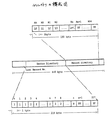
・第3の課題
半導体ディスク装置は、磁気ディスク装置をエミュレーションしているため、実デバイスが有するユーザデータ部に加えてディレクトリ(DIRECTORY)とよばれるコントロール情報部を各トラック毎に持ち、該ディレクトリにより現在エミュレートしているトラックフィールド内のレコード(ユーザデータ)に関するメモリ上のアドレスや各セクタ情報等を管理している。
チャネルアダプタは、指定されたトラックフィールドのユーザデータエリアをアクセスする場合、指定されたトラックのディレクトリをチャネルアダプタ内部に取り込むことによって、目的のトラックフィールドの制御情報を取得し、その情報に従ってユーザデータをアクセスする。このディレクトリは、▲1▼当該トラックフィールドに書き込まれているレコードのうち最終レコードのレコード番号や▲2▼セクタディレクトリ、▲3▼レコードディレクトリから成っている。セクタディレクトリは、セットセクタ処理で何番目のレコードが最初に読み出せるかが書き込まれたテーブルであり、レコードディレクトリは、各レコード毎のトラック先頭からの相対アドレス(オフセットアドレス)が書き込まれたテーブルであり、直接レコード番号で位置付けたレコードフィールドをアクセスするために用いるものである。これら情報を用いることにより、セットセクタ処理やサーチID処理時に直接オリエント(仮想ヘッド位置)を移動することができ、アクセスを高速に行うことができる。
【0007】
ところで、メモリの2ビットエラー等で目的のディレクトリ部を読み込めなくなると、当該ディレクトリが制御するトラックフィールドのユーザデータが全てアクセス不可能になってしまい、事実上、有効なユーザデータが失われてしまう。このため、データ消失回避機構として、ディレクトリが読み込み不可能な状態に陥った場合でも、ユーザデータをアクセスできるようにするデータ消失回避機構が必要になる。
従来の半導体ディスク装置では、チャネルアダプタのファームウェアが指定するトラックフィールドをアクセスしようとした時、まず当該トラックフィールドの制御情報が書き込まれているディレクトリを読み込んでから、通常処理を開始する。そのため、ディレクトリが読み込み不可能な場合、当該トラックフィールドへのアクセスをしようとしても、ディレクトリ崩壊時の回復手段がないため、アクセスが不可能である。そこで、読み込み不可能となったトラックを再度利用できるようにするために、最低単位のイニシャライズ(例えば1シリンダ単位)をして、崩壊したディレクトリを初期化し、ディレクトリを有効化してやる必要がある。しかし、イニシャライズ処理はイニシャライズする領域のユーザデータを消失させてしまうので、あらかじめイニシャライズする領域のデータを退避しておかなければならない。又、ディレクトリの崩壊によってアクセス不可能に陥ったトラックフィールドのデータはチャネルコマンドの1つとして用意されたメモリダンプ命令でしか読みだすことができない。このため、半導体ディスク装置内部のトラックフォーマットを知っている者以外は、当該トラックフィールドのユーザデータとして必要な部分を抜き出して再現することは不可能であり、完全に元のデータを復旧させることは殆ど不可能であった。
【0008】
・第4の課題
半導体ディスク装置は、データの記憶・格納媒体が半導体メモリチップである。このため、磁気ディスク装置に比較すると、ビット当りの記憶コストが高くなる。又、半導体ディスク装置1台当りの記憶容量は少なくなる。この容量に関する問題を解決するために、データを圧縮して書き込み、読み出す場合には圧縮データを復元する方法が提案されている。かかる圧縮方式の問題点は、ユーザデータを書き替える際に、圧縮後のサイズが圧縮前のサイズと異なる場合が生じることである。圧縮後のデータサイズが小さい場合には、メモリの有効利用のために余分な領域を解放する必要があり、逆に圧縮後のデータサイズが大きい場合には新たな領域を確保して書き替える必要がある。かかるメモリ管理は煩雑であり、従来は、メモリの有効利用を図りつつ、しかも簡単な方法でメモリ領域の解放、割当て管理を行うことができない問題があった。
【0009】
以上から本発明の目的は、別途保守装置を設けなくても半導体ディスク装置を運用中のまま、半導体メモリモジュールの交換ができ、しかも、半導体メモリモジュール交換中におけるアクセス速度を低下しないようにできるディスク装置を提供することである。
【0010】
【課題を解決するための手段】
上記課題は、本発明によれば、複数の半導体メモリモジュールと、予備の半導体メモリモジュールと、半導体メモリモジュールへのデータの書き込み及び読み出しを制御するチャネルアダプタと、半導体メモリモジュールへのアクセスに関して排他制御を実行する排他制御部と、各半導体メモリモジュールのメモリエラーを監視し、メモリエラーが発生した半導体メモリモジュールの記憶内容を予備の半導体メモリモジュールにコピーする際、各半導体メモリモジュールをそれぞれ複数のアクセス制御単位に分け、該アクセス制御単位でメモリエラーが生じた半導体メモリモジュールの記憶内容を予備の半導体メモリモジュールにコピーするサービスアダプタと、前記アクセス制御単位より小さい所定単位毎にコピーが正常に完了したか否かを示すコピー管理テーブルを備え、サービスアダプタは、コピーが正常に完了したか否かを示す情報を前記所定単位毎に前記コピー管理テーブルに書込み、前記チャネルアダプタはデータリード時に該コピー管理テーブルを参照し、アクセス対象である領域が正常の場合にはアクセスし、異常の場合にはアクセスせずエラーとし、又、データライト時、アクセス対象の領域にデータを書き込むと共に、該領域に応じたコピー管理データを正常とすることを特徴とするディスク装置により達成される。
【0013】
【作用】
サービスアダプタは、各半導体メモリモジュールのメモリエラーを監視し、メモリエラーが発生した半導体メモリモジュールの記憶内容を予備の半導体メモリモジュールにコピーする際、各半導体メモリモジュールをそれぞれ複数のアクセス制御単位に分け、該アクセス制御単位でメモリエラーが生じた半導体メモリモジュールの記憶内容を予備の半導体メモリモジュールにコピーする。この際、サービスアダプタは、アクセス制御単位より小さい所定単位 ( たとえばトラック単位 ) 毎にコピーが正常に完了したか否かを示す情報をコピー管理テーブルに書込み、チャネルアダプタはデータリード時に該コピー管理テーブルを参照し、アクセス対象である領域が正常の場合にはアクセスし、異常の場合にはアクセスせずエラーとし、又、データライト時、アクセス対象の領域にデータを書き込むと共に、該領域に応じたコピー管理データを正常とする。
【0018】
【実施例】
(a) 本発明の第1の実施例
(a−1) 半導体ディスク装置の構成
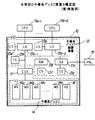
図1は本発明の半導体ディスク装置の構成図である。11a−1,11a−2,・・・はCPU(上位装置)、12は半導体ディスク装置(SSD)、13は半導体ディスク制御装置、14は半導体ディスク、15はサービスアダプタ(後述)に各種指示を出して保守を実行させるメンテナンスパネル(PNL)である。
半導体ディスク14は、複数のユーザデータ格納用の半導体メモリモジュール(MS:Main Storage)14a,14b,14c・・・14nと、半導体メモリモジュールにエラーが発生した時、該半導体メモリモジュールが新たな半導体メモリモジュールと交換されるまでその代役を勤める予備の半導体メモリモジュール(HS:Hot Spare Memory)16、各半導体メモリモジュールへのデータの書き込み/読み出しを制御するメモリインターフェースアダプタ(ESP:Extended Storage Adaptor)17を備えている。予備の半導体メモリモジュール(HS)は1枚しか示してないが、2枚以上設けることもできる。
【0019】
各半導体メモリモジュールは所定サイズ、例えばCPUからのアクセスの排他制御単位であるシリンダ単位で多数の範囲(範囲1〜範囲n)に区分されており、メモリエラー発生時にはこの範囲毎に予備の半導体メモリモジュール16への退避制御が行われ、該範囲のサイズがアクセス制御単位となる。
例えば、半導体メモリモジュール14aにエラーが発生した時の交換手順は、大略以下のようになる。
▲1▼エラーが発生した半導体メモリモジュール14aの記憶内容をアクセス制御単位に予備の半導体メモリモジュール(HS)16に退避する。排他制御はこのアクセス制御単位で行われる。
▲2▼退避完了後、予備の半導体メモリモジュール16がユーザデータ格納用の半導体メモリモジュールとなる。
▲3▼全アクセス制御単位の退避完了後に、メモリエラーが発生した半導体メモリモジュール14aを新たな半導体メモリモジュールと交換する。以後、この交換された半導体メモリモジュール14aが予備の半導体メモリモジュールとなる。尚、半導体メモリモジュール16を予備に戻すためには、▲1▼の手順と同様に半導体メモリモジュール16の記憶内容をアクセス制御単位に半導体メモリモジュール14aに復元する。
【0020】
半導体ディスク制御装置13において、13a−1,13a−2,・・・は上位装置(CPU)11a−1,11a−2,・・・との間に単一あるいは複数のインターフェース(上位インターフェース)を有するチャネルアダプタ(CA)、13bはリソースマネージャ(RM)であり、排他制御テーブルECT(図示せず)を備え、いずれのユニットも所定の半導体メモリモジュールのある領域を使用していない場合には、要求により他のユニットに半導体メモリモジュールの該領域へのアクセスを許可し、使用中の場合にはアクセスを許可しない排他制御を実行する。尚、本実施例では、リソースマネージャはアクセス制御単位で使用/未使用を管理し、該アクセス制御単位で排他制御を行う。
【0021】
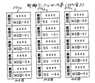
13cは各ユニットのIML(イニシャル・マイクロプログラム・ローデング)処理や状態監視処理、障害時のリカバリ処理、例えばメモリエラー発生時における半導体メモリモジュールの交換処理を行うサービスアダプタ(SA)である。13d〜13gは各種制御テーブルCTLやプログラムを記憶する制御記憶部(CS)である。制御テーブルCTLには、図2に示すように各半導体メモリモジュールの範囲(アクセス制御単位)毎に論理アドレス(CCHH)と半導体ディスクの物理アドレスの対応が記憶されている。論理アドレスとはCPUより指定されるアドレス(例えば磁気ディスクのデータアドレスで指定される場合は、シリンダ/ヘッド番号CCHH)、物理アドレスとは半導体ディスク装置内部で半導体メモリモジュールをアクセスする実アドレスである。各モジュールは制御テーブルCTLを用いて論理アドレスを物理アドレスに変換する。
【0022】
13hはコピーの成功/不成功(有効/無効)を示すコピー管理テーブルCCTを記憶する記憶部(TS)である。このコピー管理テーブルCCTは半導体メモリモジュールに書き込まれるデータのうち纏まった単位でコピーの成功/不成功を管理する。コピーが失敗した場合(媒体エラーで読めなかった場合等)、当該部分を無効とする。例えば、図3に示すようにトラック毎にコピーの成功/不成功を管理する。磁気ディスクをエミュレーションレートしている半導体ディスクの場合、シリンダ(アクセス制御単位)毎にコピーしていた場合に、エラーしてもそのシリンダ全てが無効ではない。そこで、コピー管理テーブルCCTによりトラック毎にエラーしたトラックのみ無効にすれば、きめ細かいデータの保証ができる。この場合、トラック毎でなくレコード単位で管理するとより細かいデータの保証ができる。コピー管理テーブルCCTは各モジュールが参照/更新できる場所におけばよく、半導体メモリモジュール内に配置することもできる。
【0023】
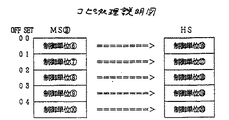
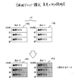
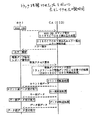
(a−2) 本発明の半導体メモリの第1の交換制御の概略
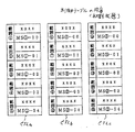
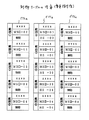
半導体ディスク14は、図4に示すように3枚の半導体メモリモジュール(MS▲1▼〜MS▲3▼)14a〜14cと、1枚の予備の半導体メモリモジュール(HS)16で構成され、それぞれ5個のアクセス制御単位で構成されている。初期時、各半導体メモリモジュール14a〜14cの制御テーブルCTLの内容は図5に示すようになっている。尚、図中、CTLaは半導体メモリモジュール14a(MS▲1▼)の制御テーブル部分、CTLbは半導体メモリモジュール14b(MS▲2▼)の制御テーブル部分、CTLcは半導体メモリモジュール14c(MS▲3▼)の制御テーブル部分である。又、図中、XXXXは論理アドレスを、MS▲1▼−00は半導体メモリモジュール14a(MS▲1▼)のオフセットアドレス00(図4参照)を意味しており、他の表記も同様である。
【0024】
半導体メモリモジュール14b(MS▲2▼)にメモリエラーが発生すると、サービスアダプタSAの制御でアクセス制御単位で半導体メモリモジュール14b(MS▲2▼)から予備の半導体メモリモジュール16にコピーが行われる。図6に示すように、コピー処理が進行して、第1、第2の制御単位▲6▼,▲7▼のコピーが終了し、第3の制御単位▲8▼のコピーは他のモジュールにより使用中のため行えず、現在第4の制御単位▲9▼をコピー中で、最後の制御単位をまだコピーしてないとすると、その時点で制御テーブルCTLの内容は図7に示すようになる。すなわち、コピーが完了した制御単位(範囲)▲6▼▲7▼の物理アドレスはコピー先の半導体メモリモジュール16の物理アドレスとなる。
以後、制御単位毎のコピーが行われ、全ての制御単位のコピーが完了すれば、制御テーブルCTLの内容は図8に示すようになる。すなわち、コピーが完了した全ての制御単位(範囲)の物理アドレスはコピー先の物理アドレスとなる。
【0025】
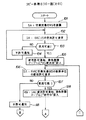
(a−3) 本発明の半導体メモリモジュールの交換制御処理
・コピー処理
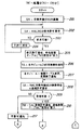
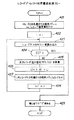
図9及び図10は半導体メモリモジュールの記憶内容を予備の半導体メモリモジュールにコピーするためのコピー処理のフロー図である。
保守パネル(PNL)15からの指示により、あるいはエラー検出管理により、サービスアダプタ(SA)13cはメモリエラー発生の半導体メモリモジュール(半導体メモリモジュール14bとする)を認識する(ステップ101)。尚、サービスアダプタSAは常時各メモリモジュールから1アドレスづつ順次データを読み出してメモリエラーが発生していないか監視している(パトロール)。1ビットエラーは元のデータに復元できるため、直ちにメモリエラー発生としないが設定値以上の1ビットエラーを検出した時メモリエラー発生と認定する。又、2ビットエラーはメモリインターフェースアダプタ(ESP)17よりサービスアダプタSAに通知される。
【0026】
サービスアダプタSAはメモリエラー発生の半導体メモリモジュールを認識すると、リソースマネージャ(RM)13bに予備の半導体メモリモジュール(HS)16の使用許可を要求する(ステップ102)。これは予備の半導体メモリモジュールHSが他の半導体メモリモジュールMSの交換作業に使用されていないことを確認するためのものである。例えば、半導体ディスク制御装置13が二重化されている場合において、他方のサービスアダプタSAが交換作業を行っている場合があるからである。
リソースマネージャRMは半導体メモリモジュールHSが使用中の場合にはサービスアダプタSAに不許可通知を出す(ステップ103,104)。これにより、サービスアダプタSAは、使用許可になる迄待つ。一方、半導体メモリモジュールHSが使用中でなければ、リソースマネージャRMは使用許可をサービスアダプタSAに通知し、内蔵の排他制御テーブルECTに「半導体メモリモジュールHSが使用中になったこと」を記入する(ステップ105)。
ついで、サービスアダプタSAはリソースマネージャRMにエラー発生の半導体メモリモジュールの第1番目のアクセス制御単位部分の使用許可を要求する(ステップ106)。
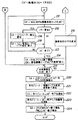
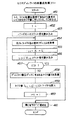
【0027】
使用可能であれば、リソースマネージャRMはサービスアダプタSAに使用許可を通知すると共に、排他制御テーブルECTに「第1番目のアクセス制御単位が使用中になったこと」を記入する(ステップ107,108)。
サービスアダプタSAは使用許可通知により、当該制御単位のコピーを実行する(ステップ109)。コピー中にエラーが発生せず、当該アクセス制御単位のコピーが完了すれば(ステップ110、111)、サービスアダプタSAは各モジュール13a−1,13a−2、13b等に制御テーブルCTLの変更を指示する(ステップ112)。すなわち、サービスアダプタSAは、制御テーブルCTLbの制御単位▲6▼における物理アドレスをHS−00に変更するように各モジュールに指示する。
各モジュールは指示された通りに制御メモリCSの制御テーブルCTLを変更し、変更完了をサービスアダプタSAに通知する(ステップ113)。尚、サービスアダプタSAも制御メモリCSの制御テーブルCTLを変更する。
【0028】
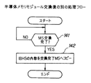
サービスアダプタSAは全モジュールから変更完了通知を受信すれば、リソースマネージャRMにアクセス終了を通知する。これによりリソースマネージャRMは、「第1番目のアクセス制御単位が不使用になったこと」を記入する(ステップ114)。ついで、サービスアダプタSAは半導体メモリモジュール14bの全制御単位のコピーが終了したチェックする(ステップ115)。
全制御単位のコピーが終了すれば、サービスアダプタSAはチャネルアダプタCAを介して上位装置CPUにコピー終了を通知すると共に、保守パネルPNLにコピー完了を表示し(ステップ116)、コピー処理を終える。コピー処理が完了すれば、保守員がメモリエラーを生じた半導体メモリモジュール(MS)14bを新たな半導体メモリモジュールと交換する。
一方、全制御単位のコピーが終了していなければ、コピー対象をコピーを終了していない別の制御単位に変更し(ステップ117)、以後ステップ106以降の処理を繰り返す。
ステップ107において、第1番目のアクセス制御単位が使用中である場合には、リソースマネージャRMはサービスアダプタSAに使用不許可通知を出す(ステップ118)。これにより、サービスアダプタSAはステップ115に飛び、以降の処理を繰り返す。
【0029】
又、ステップ110において、コピー時に所定トラックにおいてエラーが発生すれば、サービスアダプタSAはチャネルアダプタCAを介して上位装置CPUにエラー発生を通知すると共に(ステップ119)、コピー管理テーブルCCTの該当トラックにコピー不成功(無効)を記入する(ステップ120)。以後、ステップ111以降の処理を繰り返す。図11はコピーの成功/不成功を示すコピー管理テーブルCCTの説明図であり、制御単位▲6▼(半導体メモリモジュール14bの第1アクセス制御単位)のコピー管理テーブル部分を示している。尚、制御単位▲6▼は3つのトラック1〜3で構成されているものとしている。
図11(a)は制御単位▲6▼の全トラックのコピーがエラーを生じることなく成功した場合であり、コピー管理テーブルCCTのトラック1〜3には「有効」が記入される。図11(b)はトラック2のコピー時にエラーが発生した場合であり、コピー管理テーブルCCTのトラック2に「無効」が記入され、トラック1、3には「有効」が記入される。尚、コピーが不成功のトラックにデータを書き込んだ場合には、該トラックは「有効」に成り、コピー管理テーブルCCTが書き替えられる。
【0030】
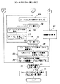
・半導体メモリモジュール交換後の処理
図12は半導体メモリモジュール交換後の処理フロー図である。
コピー完了後に保守員がエラーを生じた半導体メモリモジュールを交換すれば、サービスアダプタSAは交換完了を感知し(ステップ131)、以後、交換後の半導体メモリモジュールを予備の半導体メモリモジュールとする(ステップ132)。尚、交換完了後、保守員の保守パネルPNLからの指示により、半導体メモリモジュール16を予備の半導体メモリモジュールに戻すように構成することもできる。又、交換完了後、自動的に半導体メモリモジュール16を予備の半導体メモリモジュールに戻すように構成することもできる。図13はかかる場合の処理フロー図である。サービスアダプタSAは半導体メモリモジュールの交換完了を感知し(ステップ141)、前述のコピー処理と同様の手順で半導体メモリモジュール16の記憶データを交換後の半導体メモリモジュール14bにコピーする(ステップ142)。
【0031】
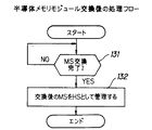
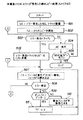
・コピー管理テーブルを用いたアクセス処理
各モジュールは半導体メモリモジュールよりレコードを読み出す場合にはコピー管理テーブルCCTを参照する。図14はコピー管理テーブルCCTを参照したアクセスの処理フロー図である。
まず、レコード読み出しか、書き込みかを判断し(ステップ151)、読み出しの場合には、アクセス先のトラックの有効/無効をコピー管理テーブルCCTを参照して調べ(ステップ152)、有効の場合には該レコードを読み出し(ステップ153)、無効の場合にはエラー処理を行う(ステップ154)。一方、書き込みの場合には、アクセス先のトラックが無効であれば「有効」に変更し(ステップ155)、しかる後、該トラックにレコードを書き込む(ステップ156)。
【0032】
以上のように、予備の半導体メモリモジュールを追加するだけで、メモリエラーが生じた半導体メモリモジュールの記憶内容を無停止で退避することができ、大がかりな保守装置を必要としない。また、半導体メモリモジュールをアクセス制御単位に細分化し、該アクセス制御単位でコピーを行うため、該制御単位で排他制御を行うことができ、コピー中であっても上位装置はコピー対象でない他のアクセス制御単位部分にアクセスすることができ、上位装置のアクセスに悪影響を与えることがない。
又、アクセス制御単位のコピーが完了する毎にサービスアダプタSAは、チャネルアダプタCA等に設けられている制御テーブルCTLにおける物理アドレスをコピー先の物理アドレスに変更するため、アクセス制御単位のコピー完了後、該アクセス制御単位については直ちにコピー先(予備の半導体メモリモジュール)にアクセスすることができる。
更に、アクセス制御単位毎にコピーが正常に完了したか否かを管理するコピー管理テーブルを設け、チャネルアダプタCA等のモジュールはデータリード時に該コピー管理テーブルを参照し、アクセス対象である領域(トラック)が正常の場合にはアクセスし、異常の場合にはアクセスせずエラーとする。この結果、コピー時にコピーエラーが発生しても誤ったデータを読み取って処理することがなく、誤動作を防止できる。
【0033】
(a−4) 本発明の半導体メモリの第2の交換制御の概略
以上は制御テーブルCTLが図2に示す構成を備えている場合である。制御テーブルCTLは図15に示すように構成することもできる。この制御テーブルCTLは、各半導体メモリモジュールの範囲(アクセス制御単位)毎に、▲1▼論理アドレス(CCHH)と、▲2▼半導体ディスクのオリジナルな物理アドレスと、▲3▼コピー先の物理アドレスを記入する欄を備えている。論理アドレスはCPU等より指定されるアドレス(例えば磁気ディスクのデータアドレスで指定される場合は、シリンダ/ヘッド番号CCHH)、オリジナルな物理アドレスは半導体ディスク装置内部で半導体メモリモジュールをアクセスする実アドレスである。通常は、論理アドレスに対応させてオリジナルな物理アドレスのみが対応付けされており、コピー先の物理アドレスは無効(マークを付けるなどして制御)となっている。
【0034】
半導体ディスク14は、図4に示すように3枚の半導体メモリモジュール(MS▲1▼〜MS▲3▼)14a〜14cと、1枚の予備の半導体メモリモジュール(HS)16で構成され、それぞれ5個のアクセス制御単位で構成されているものとする。初期時、各半導体メモリモジュール14a〜14cの制御テーブルCTLの内容は図16に示すようになっている。尚、図中、CTLaは半導体メモリモジュール14a(MS▲1▼)の制御テーブル部分、CTLbは半導体メモリモジュール14b(MS▲2▼)の制御テーブル部分、CTLcは半導体メモリモジュール14c(MS▲3▼)の制御テーブル部分である。又、図中、XXXXは論理アドレスを、MS▲1▼−00は半導体メモリモジュール14a(MS▲1▼)のオフセットアドレス00を意味しており、他の表記も同様である。
【0035】
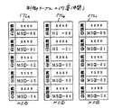
半導体メモリモジュール14b(MS▲2▼)にメモリエラーが発生すると、サービスアダプタSAの制御でアクセス制御単位で半導体メモリモジュール14b(MS▲2▼)から予備の半導体メモリモジュール16にコピーが行われる。この場合、コピーに先だって、サービスアダプタSAは各モジュールに対し制御テーブルの変更を指示する。すなわち、エラーを生じた半導体メモリモジュール14bの各論理アドレスに、▲1▼元の物理アドレスと▲2▼コピー先の物理アドレスとがそれぞれ対応するように制御テーブルの変更を指示する。これにより、各モジュールの制御テーブルCTLは図17に示すように変更される。
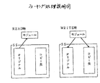
又、サービスアダプタSAは、チャネルアダプタCA等のモジュールに対して、半導体メモリモジュール14bへのアクセスに際してフォーキング処理を行うように指示する。フォーキング処理とは、図18に示すように、データ読み出しはオリジナルな物理アドレスが指示するエリアからデータを読み出し、データ書き込みは、オリジナルな物理アドレスとコピー先の物理アドレスが示す2つの記憶エリアに書き込む処理である。
【0036】
以後、図19に示すようにアクセス制御単位のコピーを行う。サービスアダプタSAは半導体メモリモジュール14bの全アクセス制御単位のコピーが終了すれば、各モジュールに制御テーブルCTLのオリジナルな物理アドレスとコピー先の物理アドレスの交換を指示する。これにより、各モジュールの制御テーブルCTLは図20に示すように変更される。以後、サービスアダプタSAは、各モジュールに対してフォーキング処理の終了を通知すると共に、コピー先の物理アドレス記入欄のアドレスを無効にするように指示してコピー処理を終了する。この結果、各モジュールの制御テーブルCTLは図21に示すようになり、オリジナルな物理アドレスはコピー先の物理アドレスとなる。
【0037】
(a−5) 本発明の半導体メモリモジュールの交換制御
・コピー処理
図22及び図23は半導体メモリモジュールの記憶内容を予備の半導体メモリモジュールにコピーするためのコピー処理のフロー図である。尚、制御テーブルCTLは図16に示すように構成されているものとする。
保守パネル(PNL)15からの指示により、あるいはエラー管理により、サービスアダプタ(SA)13cはメモリエラー発生の半導体メモリモジュール(半導体メモリモジュール14bとする)を認識する(ステップ201)。
サービスアダプタSAはメモリエラー発生の半導体メモリモジュールを認識すると、リソースマネージャ(RM)13bに予備の半導体メモリモジュール(HS)16の使用許可を要求する(ステップ202)。リソースマネージャRMは半導体メモリモジュールHSが使用中の場合にはサービスアダプタSAに不許可通知を出す(ステップ203,204)。これにより、サービスアダプタSAは、使用許可になる迄待つ。一方、半導体メモリモジュールHSが使用中でなければ、リソースマネージャRMは使用許可をサービスアダプタSAに通知し、内蔵の排他制御テーブルECTに「半導体メモリモジュールHSが使用中になったこと」を記入する(ステップ205)。
【0038】
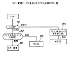
ついで、サービスアダプタSAはチャネルアダプタCA等の各モジュールに半導体メモリモジュール14bの交換開始及びフォーキング処理開始を指示する(ステップ206)。又、サービスアダプタSAは各モジュールに対し制御テーブルの変更を指示する。これにより、各モジュールは指示された通りに制御テーブルCTLを変更し(図17参照)、変更終了をサービスアダプタSAに通知する(ステップ207)。
各モジュールから制御テーブルの変更終了が通知されると、サービスアダプタSAはリソースマネージャRMにエラー発生の半導体メモリモジュールの第1番目のアクセス制御単位の使用許可を要求する(ステップ208)。
【0039】
使用可能であれば、リソースマネージャRMはサービスアダプタSAに使用許可を通知すると共に、排他制御テーブルECTに「第1番目のアクセス制御単位が使用中になったこと」を記入する(ステップ209,210)。
サービスアダプタSAは使用許可通知により、当該制御単位のコピーを実行する(ステップ211)。コピー中にエラーが発生せず、当該アクセス制御単位のコピーが完了すれば(ステップ212,213)、サービスアダプタSAはリソースマネージャRMにアクセス終了を通知する。これによりリソースマネージャRMは、「第1番目のアクセス制御単位が不使用になったこと」を記入する(ステップ214)。ついで、サービスアダプタSAは半導体メモリモジュール14bの全制御単位のコピーが終了したチェックする(ステップ215)。
全制御単位のコピーが終了していなければ、コピー対象をコピーを終了していない別の制御単位に変更し(ステップ216)、以後ステップ208以降の処理を繰り返す。
ステップ209において、第1番目のアクセス制御単位が使用中である場合には、リソースマネージャRMはサービスアダプタSAに使用不許可通知を出す(ステップ217)。これにより、サービスアダプタSAはステップ215に飛び、以降の処理を繰り返す。
【0040】
ステップ212において、コピー時に所定トラックにおいてエラーが発生すれば、サービスアダプタSAはチャネルアダプタCAを介して上位装置CPUにエラー発生を通知すると共に(ステップ218)、コピー管理テーブルCCTの該当トラックにコピー不成功(無効)を記入する(ステップ219)。以後、ステップ213以降の処理を繰り返す。
ステップ215において、半導体メモリモジュール14bの全制御単位のコピーが終了した場合には、サービスアダプタSAは各モジュール13a−1,13a−2、13b等に対して、半導体メモリモジュール14bに関係する制御テーブル部分のオリジナルな物理アドレスとコピー先の物理アドレスの交換を指示する(ステップ220)。これにより、各モジュールは制御テーブルCTLを指示通りに変更し(図20参照)、変更終了をサービスアダプタSAに通知する(ステップ221)。ついで、サービスアダプタSAは、各モジュールに対してコピー完了及びフォーキング処理の終了を通知すると共に(ステップ222)、半導体メモリモジュール14bに関係する制御テーブル部分のコピー先物理アドレス欄を無効にするように指示する(ステップ223)。各モジュールは制御テーブルCTLを指示された通りに変更する(図21参照)。これにより、オリジナルな物理アドレスはコピー先の物理アドレスとなる。
【0041】
以後、サービスアダプタSAはチャネルアダプタCAを介して上位装置CPUにコピー終了を通知すると共に、保守パネルPNLにコピー完了を表示し(ステップ224)、コピー処理を終える。コピー処理が完了すれば、保守員がメモリエラーを生じた半導体メモリモジュール(MS)14bを新たな半導体メモリモジュールと交換する。
以上のように、予備の半導体メモリモジュールを追加するだけで、メモリエラーが生じた半導体メモリモジュールの記憶内容を無停止でコピーすることができる。又、チャネルアダプタ等のモジュールはコピー中の半導体メモリモジュールにデータを書き込む際、フォーキング処理に従ってオリジナルな物理アドレスとコピー先の物理アドレスが示す2つの記憶エリアにデータを書き込むようにしたから、第1の交換制御処理のように制御単位のコピー完了毎に制御テーブルを変更する必要がなく、コピーを高速に行うことができる。
【0042】
・コピー中の制御単位エリアにライト命令が発生した場合の処理
コピー中の制御単位エリアに上位装置CPUからライト命令が発生する場合がある。かかる場合には、ライト命令をコピーが完了するまで待たせることもできるが上位装置のアクセス速度が低下する。そこで、ライト命令を優先してコピーを一時停止させるように制御する。図24はかかるコピー中の制御単位エリアにライト命令が発生した場合の処理の流れ図である。
上位装置CPUよりライト命令がチャネルアダプタCAに発行されると(ステップ251)、チャネルアダプタはアクセス制御単位についてリソースマネージャRMにアクセス許可を要求する(ステップ252)。リソースマネージャは、該アクセス制御単位がコピー中であるか調べ、コピー中でなければチャネルアダプタCAにアクセス許可を通知する(ステップ253、254)。これにより、チャネルアダプタCAはライトコマンドをフォーキング処理に従って実行する。
【0043】
一方、コピー中の場合には、リソースマネージャ255はサービスアダプタSAにコピー中の制御単位エリアに上位装置よりライトコマンドが発生したことを通知する(ステップ255)。これにより、サービスアダプタSAはコピーを停止する(ステップ256)。ついで、リソースマネージャRMはチャネルアダプタCAにアクセスを許可し(ステップ257)、チャネルアダプタCAはライトコマンドをフォーキング処理に従って実行する。
チャネルアダプタCAによる書き込みが完了すれば(ステップ258)、サービスアダプタSAは前記書き込みのアクセス単位(トラック数=Aw)とコピーのアクセス単位(トラック数=Acで例えばAc=1)の大小を比較する(ステップ259)。
Aw≧Acの場合には、サービスアダプタSAは書き込みコマンドのアクセス単位についてコピーが完了したものとみなし(ステップ260)、以後残りの部分についてコピーを再開する。
【0044】
一方、Aw<Acの場合には、書き込みコマンドのアクセス単位を包含するコピー単位は、コピーが完了していないものとみなして再度コピーし、あるいは、アクセス単位以外のコピー単位部分をコピーし(ステップ261)、以後残りの部分についてコピーを再開する。
以上のように、コピーを停止して上位装置CPUの書き込みコマンドを実行するようにしたから上位装置のアクセス速度は低下しない。又、アクセス単位がコピー単位より大きい場合には、アクセス単位部分のコピーは完了したものとみなせるからコピー速度を向上することができる。
【0045】
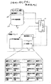
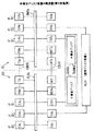
(a−6) 半導体ディスク装置の実際の構成
図25は半導体ディスク装置の全体構成図であり、二重化構成になっており、添字1を有するモジュールは第1の半導体ディスク装置G0側のモジュールであり、添字2を有するモジュールは第2半導体ディスク装置G1側のモジュール、添字の無いモジュールは共通のモジュールである。尚、制御記憶部CSは各モジュールに内蔵されている。
CAは上位装置のチャネルとのインターフェース制御を行うチャネルアダプタであり、電気チャネル、光チャネル、OCリンクに対応する種々のチャネルアダプタが適宜接続されるようになっている。RMはリソースマネージャであり排他制御、論理パス管理等の処理動作を制御すると共にサブシステム全体の資源管理を行う。SAはサービスアダプタであり、自分がマスターになり、他のユニット(モジュール)の状況を管理する。
【0046】
C−BUSは各ユニットがメッセージ通信及び制御情報のアクセスを行う制御用バス、D−BUSは各ユニットが半導体ディスクとの間でデータを授受するデータ転送用バス、S−BUSはサービスモジュールがマスターになり、各ユニットの状況を管理するサービスバスである。BH−1、BH−2はバスの競合制御、バスクロックの分配を行うバスハンドラ、MDKはメモリ障害時に該メモリの内容を一時的にバックアップする磁気ディスク装置(オプション)、DAは磁気ディスク装置とのインターフェース制御を行うデバイスアダプタ、BANKは半導体ディスク(共用メモリ)であり、半導体メモリモジュールMS,HS及び予備の半導体メモリモジュールHSが搭載されるようになっている。ESP1〜ESP4は半導体ディスクへのアクセス制御を行うポート(Extended Storage Port)、ESA1〜ESA4はESPと半導体メモリモジュールMS間のタイミング制御や、メモリのリフレッシュ、エラーチェックコードに基づくデータ修正を実行するメモリインタフェースアダプタ、PANELは保守パネルである。
【0047】
第1、第2半導体ディスク装置G0,G1は中央点線を中心に対称に構成されており、上位CPUは対称に第1、第2半導体ディスク装置のチャネルアダプタCA1,CA2に接続され、それぞれのポートESP2,ESP3は他方のメモリアダプタESA3,4と接続されている。従って、一方のチャネルアダプタに障害が生じてもCPUは他方のチャネルアダプタから半導体ディスクをアクセスすることができる。又、一方の半導体ディスクが障害を生じても他方の半導体ディスクにアクセスすることができ、信頼性を向上している。
チャネルアダプタCA,リソースマネージャRM、サービスアダプタSA等のモジュールはそれぞれマイクロプロセッサで構成されており、おおむね図26に示す構成を備えている。図において、91はマイクロプロセッサ(MPU)、92はRAM構成の制御記憶部(CS)、93はROM構成の制御記憶部(CS)、94は内部バスに接続されたドライバ/レシーバ(DV/RV)、95はバスインターフェースロジック(BIL)、96は外部インターフェースと接続されたドライバ/レシーバ(DV/RV)、97はバッファ又はテーブル記憶部(TS)、98は個別LSI(ゲートアレイ)である。尚、接続される外部インターフェースの数によってドライバ/レシーバ(DV/RV)96の数が異なる。
【0048】
(b) 本発明の第2の実施例
(b−1) 全体の構成
半導体ディスク装置は電源を切断するとその記憶内容が消失する。このため、半導体ディスク装置にバックアップディスク装置が接続される場合がある。
図27はバックアップディスク装置を備えた半導体ディスク装置の構成図であり、図1と同一部分には同一符号を付している。11a−1はCPU(上位装置)、12は半導体ディスク装置(SSD)、13は半導体ディスク制御装置、14は半導体ディスク、15はサービスアダプタSAに各種指示を出して保守を実行させるメンテナンスパネル(PNL)である。
【0049】
半導体ディスク14は、複数のユーザデータ格納用の半導体メモリモジュール(MS:Main Storage)14a,14b,14c・・・と、半導体メモリモジュールにエラーが発生した時、該半導体メモリモジュールが新たな半導体メモリモジュールと交換されるまでその代役を勤める予備の半導体メモリモジュール(HS)16を備えている。尚、17はメモリインタフェースアダプタである。
半導体ディスク制御装置13において、13a−1はチャネルアダプタ(CA)、13bはリソースマネージャ(RM)、13cはサービスアダプタ(SA)、13d,13f,13gは各種制御テーブルCTLやプログラムを記憶する制御記憶部(CS)である。18は電源切断時等において半導体ディスク14に記憶されているデータを記憶するバックアップ用の磁気ディスク装置、19は磁気ディスク装置18に半導体ディスク14に記憶されているデータを退避すると共に、退避されたデータを磁気ディスク装置より読み出して半導体ディスク14に復元するディスクアダプタである。
【0050】
(b−2) 半導体ディスクと磁気ディスクの論理ドライブ構成
半導体ディスク14を構成する各半導体メモリモジュール(MS)14a〜14cはそれぞれ1枚のプリント板で構成され、メモリバンクのスロットに挿入されている。各半導体メモリモジュール(MS)14a〜14cはそれぞれ所定サイズの複数の論理ドライブに分割されており、上位装置CPUはStart I/O命令により所定の論理ドライブを指定し、該論理ドライブが使用可能であれば該論理ドライブの所定位置にアクセスするようになっている。
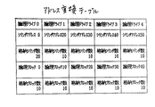
図28は半導体ディスク14と磁気ディスク装置18の論理ドライブの構成図である。半導体ディスク14は2枚の半導体メモリモジュール14a,14bで構成されているものとしており、第1半導体メモリモジュール14aは3つの論理ドライブ0〜3を備え、それぞれのサイズは10シリンダとなっている。又、第2の半導体メモリモジュール14bは10シリンダサイズの2つの論理ドライブ3〜4を備えている。
【0051】
磁気ディスク装置18における論理ドライブの構成は矢印で示すように半導体ディスク14の論理ドライブ構成と1:1の対応関係がある。すなわち、磁気ディスク装置18の論理ドライブ構成と半導体ディスク14の論理ドライブ構成は同一になっている。
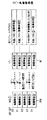
半導体ディスク14における論理ドライブの構成を示す第1の構成情報テーブル21は、論理ドライブ0〜4毎に先頭アドレス(シリンダアドレス)及び容量(シリンダ数)を保持しており、所定の半導体メモリモジュール(マスターモジュール)14aに格納されている。又、ディスク装置18における論理ドライブの構成を示す第2の構成情報テーブル22は、第1の構成情報テーブル21と同一の構成を有し磁気ディスク装置18に記憶されている。
【0052】
半導体ディスク14に記憶されているデータを磁気ディスク装置18に退避させる場合には、ディスクアダプタ(DA)19は第1、第2の構成情報テーブル21,22を読み取る。ついで、該第1の構成情報テーブル21を参照して第i論理ドライブ(i=0〜4)のデータを半導体ディスク14より読み取り、該データを第2の構成情報テーブル22を参照して磁気ディスク装置18の第i論理ドライブ(i=0〜4)に格納する。
又、磁気ディスク装置18に退避されているデータを半導体ディスク14に復元させる場合には、ディスクアダプタ(DA)19は第1、第2の構成情報テーブル21,22を読み取る。ついで、該第2の構成情報テーブル22を参照して第i論理ドライブ(i=0〜4)のデータを磁気ディスク18より読み取り、該データを第1の構成情報テーブル21を参照して半導体ディスク14の第i論理ドライブ(i=0〜4)に格納する。
【0053】
(b−3) 半導体ディスク14の論理ドライブ構成を変更した場合の問題点
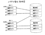
ところで、半導体ディスク14のデータを磁気ディスク装置18に退避した後に、半導体ディスク14の論理ドライブ構成を変更したい場合がある。図29は論理ドライブ構成の変更説明図であり、(a)は変更前の構成、(b)は変更後の構成であり、論理ドライブ0のサイズを10シリンダから20シリンダに増加し、論理ドライブ1〜論理ドライブ4の先頭アドレスを変更した場合である。
半導体ディスク14の構成を前記のように変更すると、従来装置では半導体ディスク14と磁気ディスク18の第1、第2の構成情報テーブル21、22は図30に示すようになる。この結果、磁気ディスク18に退避されているデータを半導体ディスク14に復元すると、矢印に示すように復元され、正しくデータの復元ができなくなる。すなわち、磁気ディスク18に退避されている論理ドライブ0、1のデータ(点線で囲んである)が半導体ディスク14の論理ドブ0に復元され、論理ドライブ2のデータが論理ドライブ1に復元され、論理ドライブ3のデータが論理ドライブ2に復元され、論理ドライブ4のデータが論理ドライブ3に復元されてしまう。この結果、退避したデータを使用できなくなる。
以上は、論理ドライブのサイズを変更した場合であるが、図31に示すように論理ドライブの配置を変更した場合も同様の問題点が生じる。
【0054】
(b−4) 本発明の復元処理の概略
図32はデータ退避後に半導体ディスク14の論理ドライブ構成を変更した場合における本発明の復元処理の概略説明図である。14は半導体ディスク、18は磁気ディスク装置19はディスクアダプタである。半導体ディスクディスク14において、20はユーザデータ格納領域、21は半導体ディスクの論理ドライブ構成を保持する第1構成情報テーブル、23は後述するアドレス変換テーブルである。磁気ディスク装置18において、22は磁気ディスクの論理ドライブ構成を保持する第2構成情報テーブル、24はユーザデータ格納領域である。半導体ディスク14及び磁気ディスク18は初期時に図28に示す構成を備えている。
半導体ディスク14のデータを磁気ディスク18に退避した後、保守パネル(PNL)15からの指示により半導体ディスク14の構成を図29(b)に示すように変更する。この結果、半導体ディスク14の第1の構成情報テーブル21は図30に示すようになる。
【0055】
ついで、保守パネルPNLより復元が指示されると、ディスクアダプタ(DA)19は、半導体ディスク14及び磁気ディスク18より第1、第2の構成情報テーブル21、22を読み取り、これら第1,第2の構成情報テーブル21,22を用いて、論理ドライブ毎にディスクアドレスを半導体メモリのアドレスに変換するためのアドレス変換テーブル23(図33参照)を作成する。このアドレス変換テーブル23は論理ドライブ毎に▲1▼半導体ディスク14の先頭アドレス、シリンダ数、及び▲2▼磁気ディスク18の先頭アドレス、シリンダ数を持たせたものである。
しかる後、ディスクアダプタDAは図34に示すようにアドレス変換テーブル23を参照して第i論理ドライブ(i=0〜4)のデータを磁気ディスク18より読み取り、該データをアドレス変換テーブル23が指示する半導体ディスク14の第i論理ドライブ(i=0〜4)に格納する。以上により、磁気ディスク18に退避してある各論理ドライブのデータを構成変更後の論理ドライブに復元でき、該データを使用することができる。
復元完了後に、磁気ディスク装置18の第2の構成情報テーブル22を半導体ディスク14の第1の構成情報テーブル21に一致させる。
【0056】
(b−5) 本発明の復元処理
図35は本発明の復元処理のフロー図である。
データを磁気ディスク装置18に退避した後に、半導体ディスク14の論理ドライブ構成を変更したい場合には、保守パネル(PNL)15より構成情報変更コマンドと論理ドライブの構成情報を入力する(ステップ301)。これにより、サービスアダプタSAは半導体ディスク14に記憶されている第1の構成情報テーブル21を更新する(ステップ302)。しかる後、磁気ディスク装置18に退避してあるデータを半導体ディスク14へ復元するために、保守パネルPNLよりリストアコマンドを入力する(ステップ303)。サービスアダプタSAはリストアコマンドが入力されると、ディスクアダプタ(DA)19に対して、アドレス変換テーブル23の作成を指示する(ステップ304)。
【0057】
ディスクアダプタDAは半導体ディスク14及び磁気ディスク装置18より第1、第2の構成情報テーブル21、22を読み取り、これら第1,第2の構成情報テーブル21,22を用いてアドレス変換テーブル23(図32参照)を作成し、半導体ディスク14に記憶する(ステップ305)。ついで、ディスクアダプタDAは該アドレス変換テーブル23を参照して第i論理ドライブ(i=0〜4)のデータを磁気ディスク18より読み取り、該データをアドレス変換テーブル23が指示する半導体ディスク14の第i論理ドライブ(i=0〜4)に格納する(ステップ306、307)。
【0058】
全データの半導体ディスク14への復元が完了すれば、保守パネルPNLより構成情報合わせ込みコマンドを発行する(ステップ308)。サービスアダプタSAは構成情報合わせ込みコマンドが発行されると、ディスクアダプタDAに第2の構成情報テーブル22の変更を指示する(ステップ309)。これにより、ディスクアダプタDAは半導体ディスク14より第1の構成情報テーブル21を読み出し、第1、第2の構成情報テーブル21,22が1:1に対応するように第2の構成情報テーブル22を作成し、磁気ディスク18に記憶されている内容を更新する(ステップ310)。
以上より、半導体ディスクの構成を変更しても、構成変更前にバックアップディスク装置に退避したデータを構成変更後の半導体ディスク装置に正しく復元でき、変更前のユーザデータが使用することができる。
【0059】
(c) 本発明の第3の実施例
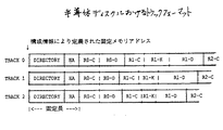
(c−1) トラックフォーマット、ディレクトリ及びカウント部の構成
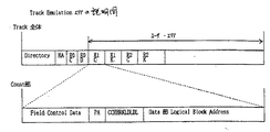
・トラックフォーマット
半導体ディスク装置では、各トラックフィールドの先頭にディレクト(コントロール情報部)が設けられている。チャネルアダプタCAは指定されたトラックフィールドのユーザデータをアクセスする場合、該トラックフィールドのディレクトリを読み込み、該ディレクトリを用いてユーザデータをアクセスする。
図36は半導体ディスクにおけるトラックフォーマットの例であり、各トラックの先頭にはディレクトリ(DIRECTORY)が配置され、その後にホームアドレス(HA)が置かれ、以降にCKDフォーマットにしたがった可変長のレコード(RECORD−0,RECORD−1,・・・)が配列されている。ホームアドレスHAはトラックアドレス(CCHH)を示すものであり、各レコードはカウント部C、キー部K、データ部Dで構成されている。
【0060】
・ディレクトリ
ディレクトリは図37に示すように448バイトを有し、▲1▼1バイトの最終レコード番号(LAST RECORD NO.)、▲2▼218バイトのセクタディレクトリ(SECTOR DIRECTORY)、▲3▼190バイトのレコードディレクトリ(RECORD DIRECTORY)、▲4▼その他有効性を確認するためのID部等のエリア、▲5▼未使用エリアで構成されている。
最終レコード番号(LAST RECORD NO.)はトラックフィールドに書き込まれている最後のレコードのレコード番号を示すものである。各トラックフィールドの最終レコードの直後にはエンドマーク(EOF)が書き込まれており、最終レコードはこのエンドマークを読み込む直前のレコードということになる。そして、最終レコードのレコード番号が最終レコード番号と成る。
【0061】
セクタディレクトリ(SECTOR DIRECTORY)は、セットセクタ処理で最初に読める物理レコード番号をセクタ値別に格納したものである。物理レコード番号とは、ホームアドレスHAを0として、論理レコード番号に1を加えた値である。トラックは例えば218のセクタに区分され、それぞれセクタ値0〜217迄の値が割り当てられる。セクタ値217はトラックを所定サイズのセクタで分割した時の最後のセクタを示すもので、最大セクタ値である。このセクタディレクトリ(SECTOR DIRECTORY)はセットセクタ命令に対するセットセクタ処理において使用され、セクタ処理で何番目のレコードが最初に読み出せるかを示す。尚、実際は0〜221のセクタが存在する。但し218〜221はレコード配置の関係上これ以降にレコードがくることはないのでセクタディレクトリには存在しない。
レコードディレクトリ(RECORD DIRECTORY)は各レコード(レコード0〜レコード94)までのトラック先頭からのオフセットアドレスを2バイトで示すものである。トラックの先頭アドレスに目的レコードのオフセットアドレスを加えることにより、該目的レコードのカウント部のメモリアドレスを求めることができる。レコード番号94はトラックに書き込める最大のレコード数を示す。このレコードディレクトリ(RECORD DIRECTORY)は、セクタ処理で取得したレコード番号のフィールドの読み出しや直接レコード番号を指定してレコードを読み出す際に使用される。
【0062】
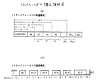
・カウント部
各レコードは前述のように、カウント部C、検索のためのキーが記録されるキー部K(必ずしも必要でない)、ユーザデータが記録されるデータ部Dで構成されている。カウント部Cは図38に示すように64バイトを有し、▲1▼ホストから与えられる8バイトの実データ部、▲2▼データの保証のために前後に付加される各4バイトのID部、▲3▼トラックフィールドをアクセスするための48バイトのコントロール情報部より成っている。実データ部には、トラックアドレス(CCHH)、レコード番号(R)、及び後に続くキー部の長さ(KL)、データ部の長さ(DL)が記録される。ID部にはレコードの先頭を識別するコードや、データが書き込まれた最新の時刻(タイムスタンプ)等が記録される。コントロール情報部は、ディレクトリが消失しても目的レコードを検索し、かつ、ディレクトリの一部を復元できるようにするためにディレクトリ復元データ(制御情報復元データ)が記録されている。ディレクトリ復元データには、▲1▼自分のレコードの先頭から次のレコード先頭迄の相対アドレス(オフセットアドレス)Aiと▲2▼自分のレコードが位置するセクタのセクタ値Siが含まれている。
【0063】
ディレクトリ、ホームアドレス、各レコードのカウント部の長さは一定のため、ディレクトリ、HA及びRECORD−0のカウント部はトラック先頭から決まった相対位置にある。図39(a)に示すようにトラック先頭からホームアドレスHAまでのオフセットアドレスL0,レコードRi−1迄のオフアドレスをLiとすると、これらオフセットアドレスLi(i=0,1,2,・・・)はレコードディレクトリ(RECORD DIRECTORY)に記録される(図37参照)。この場合、レコードRi−1からレコードRi迄のオフセットアドレスをAiとすると、該オフセットアドレスAiはディレクトリ復元データとしてレコードRiのカウント部に記録される。Ai,Li間には次式
Li+Ai→Li+1
の関係が成立する。
【0064】
又、セクタとレコードの関係が図39(b)に示すようになっているものとすると、セクタディレクトリ(SECTOR DIRECTORY)におけるセクタ値0に対応させて0(HA)が、セクタ値1〜2に対応させて1(レコードR0)が、セクタ値3〜6に対応させてレコード2(R1)が、セクタ値7〜13に対応させて3(レコードR2)が・・・記録される。すなわち、セクタiにレコードRjが存在すれば、セクタ値iに対応させてレコードRj+1がセクタディレクトリに記録される。そして、レコードRjがセクタi〜(i+m)に位置すると、セクタ値i〜(i+m)がディレクトリ復元データとしてレコードRj+1のカウント部に記録される。
【0065】
(c−2) レコード読み取り、書き込み手順
図40は半導体ディスク装置のレコード読み取りシーケンス説明図である。尚、半導体ディスク装置は図1と同一構成を備えているものとする。
上位装置CPUよりシークコマンドSKが発生すると、チャネルアダプタCAは直ちに動作終了信号を上位装置に返す。上位装置CPUは動作終了信号を受信すれば、つぎにセットセクタコマンドSSを発行する。以後、同様にして上位装置はサーチIDコマンドSIDを発行し、チャネルアダプタCAはこれらコマンドを受信する。
チャネルアダプタCAはサーチIDコマンドを受信すると、シ−クコマンドで指示されている論理アドレス(トラックアドレスCCHH)を半導体ディスクの物理アドレスに変換する。この物理アドレスはトラックの先頭アドレス、換言すればディレクトリの先頭アドレスを示しているから、半導体ディスクよりディレクトリを読み込む。
【0066】
ついで、セットセクタコマンドで指示されているセクタ値に応じたレコード番号をセクタディレクトリより求める(セットセクタ動作)。しかる後、該レコード番号のアドレスをレコードディレクトリより求め、該アドレスよりレコードのカウント部を読み取る。ついで、該カウント部に含まれるレコードのCCHHRとサーチIDコマンドで指示されている目的レコードのCCHHRが一致するかチェックし、一致すればサーチID動作を終了する。一致しない場合には次のレコード番号のレコードを読み取って同様の処理を行う。
目的のレコードが見つかれば、チャネルアダプタCAは上位装置に動作終了信号を返す。これにより上位装置はリードコマンド(READ CKD)を発行し、チャネルアダプタCAは該コマンドを受信する。以後、チャネルアダプタCAはカウント部C、キー部K、データ部Dを順次上位装置CPUに転送し、最後に正常終了を送って一連のレコードリード処理を終了する。
【0067】
図41は半導体ディスク装置のレコード書き込みシーケンス説明図であり、サーチ動作迄はレコード読み取り手順と同一である。
サーチID動作により目的とするレコードが見つかれば、チャネルアダプタCAは上位装置に動作終了信号を返す。これにより上位装置はライトコマンド(WRITE CKD)を発行し、チャネルアダプタCAは該コマンドを受信する。以後、チャネルアダプタCAは、ディレクトリ復元データ(制御情報復元データ)Ai,Siを求めてカウント部に挿入し、しかる後、レコードを記録する。
レコード記録完了後、チャネルアダプタCAは上位装置CPUに書き込み終了を通知する。通知後、ディレクトリの内容を更新し、ディレクトリが記録されていた半導体ディスク位置に書き戻す。
【0068】
(c−3) ディレクトリの読み込みエラーが発生した場合の処理
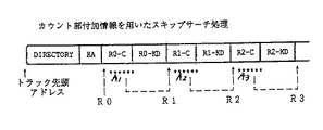
▲1▼スキップサーチ処理
レコードの読み込み、書き込み時に、チャネルアダプタCAがディレクトリを読み込めなくなった場合には、各レコードのカウント部に記録されているディレクトリ復元データを用いて目的とするレコードをサーチ(スキップサーチ)する。尚、ディレクトリが読み込めなくなった場合としては、2ビットエラーの発生、IDエラーの発生(ディレクトリの書き込み失敗)等があり、かかるエラー発生時、チャネルアダプタCAはディレクトリを取り込むことができず、通常のアクセスができなくなる。
図42はチャネルアダプタCAがディレクトリを読み込めなくなった場合のスキップサーチ処理のフロー図、図43はスキップサーチ処理の説明図である。
まず、チャネルアダプタは1→iとする(ステップ401)。ついで、チャネルアダプタCAはアドレスLi−1(=L0)よりレコードRi−1(=R0)のカウント部C0を読み込む(ステップ402)。なお、レコードR0のトラック先頭からの記憶位置は固定でL0は既知である。
【0069】
カウント部の読み込み後、該カウント部に含まれるているレコード番号がアクセス指示されたレコード番号Nと等しいかチェックする(ステップ403)。等しければ、レコードRi−1が目的とするレコードであり、該レコードを読み込み、あるいは書替えを行う(ステップ404)。
しかし、カウント部に記録されているレコード番号がアクセス指示されたレコード番号Nと等しくなければ、カウント部に記録されている次のレコードRi迄の相対アドレス(オフセットアドレス)Aiを取得する(ステップ405)。
ついで、次式
Li−1+Ai→Li
により、レコードRiのトラック先頭からのオフセットアドレスLiを演算し(ステップ406)、Li演算後iを歩進し(i+1→i、ステップ407)、以後ステップ402以降の処理を繰り返す。以上により、最終的にステップ403においてカウント部に記録されているレコード番号がアクセス指示されたレコード番号Nと等しくなり、目的とするレコードが求まり、該レコードの読み込み、あるいは書替えを行う。
以上のようにすれば、上位装置CPUより指示されたレコードの読み取りあるいは書き込み時に、ディレクトリを読み込めなくなってもチャネルアダプタCAは自動的に各レコード中に記録されているディレクトリ復元データを用いて上位装置より指示された目的レコードをサーチして該レコードの読み取りあるいは書き込みを行うことができる。
【0070】
▲2▼ディレクトリの再構築
ディレクトリを読み込めなくなった場合には、上記スキップサーチ法により目的とするレコードをサーチすることができる。この場合、スキップサーチ処理と並行してディレクトリ復元データを用いてディレクトリを再構築することができる。
・レコードディレクトリの再構成処理
図44はレコードディレクトリの再構成処理フロー図である。
まず、ホームアドレスHA、レコードR0のオフセットアドレスとしてL0,L1(固定値)をレコードディレクトリにセットする(ステップ421)。しかる後、iを1にセットし、レコードRi−1のカウント部を読み込む(ステップ422,423)。
ついで、読み込んだ情報がエンドマーク(EOF)でないかチェックし(ステップ424)、EOFでなければ、カウント部より次のレコードRi迄の相対アドレス(オフセットアドレス)Aiを取得する(ステップ425)。
【0071】
Aiが求まれば、次式
Li−1+Ai→Li
により、レコードRiのトラック先頭からのオフセットアドレスLiを演算する(ステップ426)。ついで、LiをレコードRiの先頭からのオフセットアドレスとしてレコードディレクトリにセットし(ステップ427)、iを歩進し(i+1→i、ステップ428)、以後ステップ423以降の処理を繰り返す。
以上の処理を繰り返せば、いつかステップ424においてエンドマークがEOFが検出される。エンドマークが検出されればレコードディレクトリにおける残りを”FF”で埋める(ステップ425)。
以上によりレコードディレクトリを復元することができる。
【0072】
・セクタディレクトリの再構成処理
図45はセクタディレクトリの再構成処理フロー図である。
ホームアドレスHA、レコードR0のカウント部の位置は固定である。従って、セクタディレクトリにおける最初の幾つかのセクタ値に対応させてH0,R0をセットする(ステップ451)。
ついで、iを1にし、レコードRi−1のカウント部を読み込む(ステップ452,453)。しかる後、カウント部より次のレコードRi迄の相対アドレス(オフセットアドレス)Aiを取得する(ステップ454)。
【0073】
Aiが求まれば、次式
Li−1+Ai→Li
により、レコードRiのトラック先頭からのオフセットアドレスLiを演算する(ステップ455)。ついで、レコードRiのカウント部を読み込み(ステップ456)、読み込んだ情報がエンドマーク(EOF)でないかチェックする(ステップ457)。EOFでなければ、レコードRiのカウント部より該レコードRiの先頭セクタ値Siを取得する(ステップ458)。ついで、セクタディレクトリにおけるセクタ値Siに対応させてレコードRiを記入し(ステップ459)、しかる後、iを歩進し(i+1→i、ステップ460)、ステップ454以降の処理を繰り返す。
【0074】
以上の処理を繰り返せば、いつかステップ424においてエンドマークがEOFが検出される。エンドマークが検出されればセクタディレクトリにおける残りを”FF”で埋める(ステップ461)。以上によりセクタディレクトリを復元することができる。
以上のようにすれば、上位装置CPUより指示されたレコードの読み取りあるいは書き込み時に、ディレクトリを読み込めなくなるエラーが発生した場合であっても、チャネルアダプタCAは自動的にディレクトリ復元データを用いてディレクトリを再構築するから、次のアクセスに際して該ディレクトリを参照して高速のアクセスが可能となる。
【0075】
図46は、ディレクトリにエラーが発生した場合の全体の概略シーケンスの説明図である。上位装置(ホスト)CPUよりレコード読み取り命令READ Dが発行されると、チャネルアダプタCAは該コマンドを受け付け、ディレクトリの読み込み処理を行う。ディレクトリの読み込みエラーが発生すると、チャネルアダプタCAはアクセス法を通常のディレクトリ使用のアクセス法からスキップサーチ法に切り替える。以後、図42に示す手順に従って目的とするレコードをスキップサーチし、目的レコードが求まればデータ部を上位装置に転送する。この場合、スキップサーチ処理と並行して図44及び図45のレコードディレクトリ、セクタディレクトリの再構成処理を行ってディレクトリを再構築することもできる。
【0076】
(c−4) ディレクトリにエラーが発生した場合の別の処理
以上では、ディレクトリにエラーが発生した場合、自動的に目的のレコードをサーチして読み/書きし、またディレクトリを再構築した場合について説明した。しかし、かかる目的レコードのサーチやディレクトリの再構築は上位装置CPUからの指示に従って行うようにしても良い。
図47はかかる場合のレコードリード手順説明図である。
上位装置(ホスト)CPUよりレコード読み取り命令READ CKDが発行されると、チャネルアダプタCAは該コマンドを受け付け、ディレクトリの読み込み処理を行う。この場合、ディレクトリの読み込みエラーが発生すると、チャネルアダプタCAはエラー情報を作成して上位装置にエラー報告を行う。
【0077】
上位装置CPUはエラーを解析し、特殊ダンプコマンドとレコード番号NをチャネルアダプタCAに発行する。チャネルアダプタCAは特殊ダンプコマンドを受け付け、図42に示す手順に従って目的とするレコードをサーチし、目的レコードが求まれば、カウント部、キー部、データ部を順次上位装置に転送する。
以上は、特殊ダンプ命令による処理にディレクトリ再構築処理が伴わない場合である。ディレクトリ再構築処理が伴う場合には、図44及び図45のレコードディレクトリ、セクタディレクトリの再構築処理を行い、ディレクトリを再構築し、対象トラックの先頭に書き込む。
【0078】
(c−5) コピー時にディレクトリエラーが発生した場合の処理
半導体ディスク装置にメモリ障害を生じると、サービスアダプタSAの制御によりエラーが生じた半導体メモリモジュールMSの内容を予備の半導体メモリモジュールHSにコピーし、しかる後、障害を生じた半導体メモリモジュールを新たな半導体メモリモジュールと交換する(第1実施例、図1参照)。
かかる場合、エラーが発生したトラック以外のコピーはサービスアダプタSAが行い、エラーが発生したトラックフィールドのコピーについてはチャネルアダプタCAに依頼して該当チャネルアダプタCAが行う。
というのは、サービスアダプタSAはフィールド単位の処理ができず、固定長(64バイト)毎のブロックコピーをする。このため、エラーが発生したトラックフィールドのコピーについて、同様のコピー処理を行ってもエラー発生情報をディレクトリや各カウント部付加情報に書き込めず、ユーザデータのアクセスは保証できないものになってしまうからである。そこで、サービスアダプタSAはメモリ障害が発生したトラックフィールドのコピー処理についてはチャネルアダプタCAに依頼し、依頼を受けたチャネルアダプタCAは、ディレクトリから順にエンドマークEOFまでフィールド単位でコピー処理を行う。
【0079】
チャネルアダプタCAはコピーの途中でメモリ障害を起こしているフィールド(カウント部、キー部、データ部)を発見すると、そのフィールド(カウント部の場合にはレコード全体)のみを無効化し、カウント部における必要な制御情報の書替えを行う。しかし、ディレクトリ部がメモリ障害を起こしている場合にディレクトリを無効化してしまうと、当該トラックフィールド上の全てのレコードが無効化してしまい、更にはチャネルアダプタCAもディレクトリを読み込めないためトラックのフォーマットを判断できない。
【0080】
これを回避するために、チャネルアダプタCAは、固定位置のHAフィールド及びレコードR0をコピーし、レコードR1以降のフィールドに関しては、スキップサーチ方法により次のレコードフィールドのアドレスを取得しながらエンドマークまでコピーを行う。すなわち、現レコードのカウント部を読み込めば、ディレクトリの再構築に必要な次のレコード迄のオフセットアドレスや現レコードのセクタ値、現レコードのキー長、データ長を取得でき、現レコードフィールドのコピーを行って次のレコードの処理に移れる。これをエンドマーク検出まで続けるとディレクトリを除く全てのフィールドのコピーができる。更に、上記コピー処理はディレクトリ再構築のために必要な全てのレコード部のディレクトリ復元データの読み込み処理を含んでいるため、必然的にディレクトリを再構築することができる。そこで、各フィールドのコピー処理をすると同時にディレクトリの再構築処理を行い、最後にチャネルアダプタCA内部で再構築したディレクトリをコピー先のディレクトリ領域に書き込むことでメモリ交換処理時のユーザデータ消失を防止することができる。
【0081】
図48及び図49は半導体メモリにエラーが生じた時のコピー処理のフロー図である。尚、半導体ディスク装置は図1に示す構成を有しているものとする。
サービスアダプタSAはエラーが発生した半導体メモリモジュールMS及びトラックを認識すると(ステップ501)、該半導体メモリモジュールMSのコピーを開始する(ステップ502)。
コピー対象トラックがエラー発生トラックであるかチェックし(ステップ503)、エラー発生トラックでなければ該トラックのコピーを実行し(ステップ504)、コピー完了後半導体メモリモジュールMSのコピーが完了したチェックし(ステップ505)、完了していれば次のトラックについてステップ503以降の処理を行う。
【0082】
一方、ステップ503において、コピー対象トラックがエラー発生トラックの場合には、該エラー発生トラックのコピーをチャネルアダプタCAに依頼する(ステップ506)。チャネルアダプタCAはフィールド単位でのコピーを開始し、フィールドの読み込みを行う(ステップ507)。該フィールドでエラーを検出すれば(ステップ508)、ディレクトリのエラーかチェックし(ステップ509)、ディレクトリのエラーでない場合には当該フィールドを無効化し(ステップ510)、ステップ507に飛ぶ。しかし、ディレクトリのエラーであればフラグFを”1”にし(”1”→F、ステップ511)、ステップ507に飛ぶ。
ステップ508において、フィールドにエラーが存在しない場合には、該フィールドのコピーを実行し(ステップ512)、ついで、F=”1”かチェックし(ステップ513)、F=”1”の場合にはディレクトリの再構築処理を行う(ステップ514)。
【0083】
しかる後、エンドマークEOFが検出されたチェックし(ステップ515)、検出してなければステップ507に飛び以降のフィールドのコピーを実行する。
エンドマークEOFが検出された場合には、F=”1”かチェックし(ステップ516)、F=”0”の場合にはサービスアダプタSAにコピー終了を通知する(ステップ517)。これにより、サービスアダプタは次のトラックに対してステップ503以降のコピー処理を繰り返す。
ステップ516において、F=”1”の場合には、再構築したディレクトリをコピー先のディレクトリ領域に書き込み(ステップ518)、ついでFを”0”にし(”0”→F、ステップ519)、サービスアダプタSAにコピー終了を通知する(ステップ517)。これにより、サービスアダプタは次のトラックに対してステップ503以降のコピー処理を繰り返す。
【0084】
以上のように、第3実施例によれば、ディレクトリを読み込めなくなっても、該ディレクトリを用いずに各レコードに含まれる制御情報復元データを用いて上位装置により指示された目的レコードへのアクセスが可能となる。又、制御情報復元データを用いてディレクトリの再構築ができるため、以後、再構築したディレクトリを用いてアクセスができる。このため、アクセス速度が低下することはない。
又、メモリエラーによる半導体メモリモジュール交換時のコピー処理において、ディレクトリを読み込めなくなるエラーが検出された場合にも、各レコードに含まれる制御情報復元データを用いて順次次のレコード位置が判明するためレコードのコピーができ、しかも、ディレクトリを再構築してコピー先のディレクトリ領域に書き込むことができる。
【0085】
(d) 第4実施例
(d−1) 全体の構成
図50はデータを圧縮して半導体ディスクに記憶する半導体ディスク装置の実施例の構成図であり、二重化構成になっており、添字1を有するモジュールは第1の半導体ディスク装置G0側のモジュールであり、添字2を有するモジュールは第2半導体ディスク装置G1側のモジュール、添字の無いモジュールは共通のモジュールである。
【0086】
CA1,CA2は上位装置のCPU、チャネルとのインターフェース制御を行うチャネルアダプタであり、上位装置(チャネル)に接続されるようになっている。RM1,RM2はリソースマネージャであり排他制御等の処理動作を制御すると共にサブシステム全体の資源管理を行う。TS1,TS2は排他制御テーブル等のテーブル類を記憶するテーブルストーリッジ(テーブル記憶部)、SA1,SA2はサービスアダプタ、MDKは半導体ディスクの内容を一時的にバックアップする磁気ディスク装置、DA1,DA2は磁気ディスク装置とのインターフェース制御を行うデバイスアダプタ、BANK1,BANK2は半導体ディスクであり、複数の半導体メモリモジュール及び予備の半導体メモリモジュールが搭載されるようになっている。ESP1,ESP2は半導体ディスクへのアクセス制御を行うポート、MT1,MT2は半導体メモリを多数の所定サイズのブロックに分割した時、各ブロックの使用/未使用状態を記憶する半導体メモリテーブル、MCA1,MCA2は半導体メモリにおけるブロック毎の使用/未使用状態を管理し、チャネルアダプタCA1,CA2からのブロック要求により未使用ブロックを割り当て、該ブロックを使用中にすると共に、チャネルアダプタからのブロック解放要求により所定の使用中ブロックを未使用中に変更する。
【0087】
BUS1,BUS2はバスであり、制御用バス、データ転送用バス、サービスバスを有している。CBUSは一方のテーブル記憶部TS1(TS2)の内容が変化した時、直ちに他方のテーブル記憶部TS2(TS1)にコピーするコピーバス、CBUS′は一方の半導体メモリテーブルMT1(MT2)の内容が変化した時、直ちに他方の半導体メモリテーブルMT2(MT1)にコピーするコピーバスである。
第1、第2半導体ディスク装置G0,G1は中央点線を中心に対称に構成されており、上位CPUは対称に第1、第2半導体ディスク装置のチャネルアダプタCA1,CA2に接続されている。
【0088】
(d−2) 半導体メモリの構成
半導体メモリBANKは図51に示すように、トラックエミュレーションエリア51と、レコードのうちデータ部を圧縮して記憶する圧縮データ格納エリア52に分けられている。圧縮データ格納エリア52は所定サイズの多数のブロック(論理ブロック)に分割され、各レコードのデータ部は圧縮された後、必要数のブロックに連続的にあるいは分散して格納される。
【0089】
トラックエミュレーションエリア51の各トラックはレコードのデータ部が記憶されない点を除けば、図36に示すトラックフォーマットを備えている。各トラックフィールドには図52に示すように、ディレクトリ、ホームアドレスHA、レコード0のカウント部及びデータ部、各レコードのカウント部、キー部が記憶される。各レコードRi(i=1,2・・・)のカウント部Cにはフィールドを制御する制御情報やレコード番号CCHHR、キー長KLデータ長DL等が書かれ、更に、データ部が記憶される圧縮データ格納エリア52のブロック番号(ブロックアドレス)が書かれるようになっている。
レコードを書き込は、図53に示すように書き込むべきレコードのデータ部DTを圧縮して圧縮データDT′とし、ついで、該圧縮データDT′のサイズに応じた数のブロック(図では3つ)確保し、該確保したブロックB1〜B3に圧縮データDT′の第1〜第3部分▲1▼〜▲3▼を格納し、これらブロックB1〜B3のブロックアドレスをカウント部に挿入してトラックエミュレーションエリア51に格納する。
【0090】
(d−3) チャネルアダプタの構成
図54は圧縮/復号処理を行うチャネルアダプタの構成図である。チャネルアダプタ内部において、61は非圧縮データを記憶する大容量(例えば1トラック分)の第1データバッファ、62は圧縮データを記憶する大容量(例えば1トラック分)の第2のデータバッファ、63はデータの圧縮・復号を行うデータ圧縮機構部、64は圧縮・復号動作を補助する辞書メモリ、64はチャネルインターフェースプロトコル制御部、65は第1、第2のデータバッファからのデータを選択して出力すると共に、逆にデータを第1、第2のデータバッファに選択的に出力するセレクタ、66は半導体ディスク装置内部の他のユニットと接続された内部バスを制御する内部バスインターフェース制御部(BIL)、67は非圧縮データのバイト数を計数する第1のカウンタ、68は圧縮データのバイト数を計数する第2のカウンタ、69はこれらハードウェア資源をマイクロプログラムにより制御するMPU、70はプログラム、制御テーブルその他のテーブル類を格納するコントロールストレージ、71はバスである。
【0091】
(d−4) レコード読み取り処理
図55はレコード読み取り処理のシーケンス説明図である。
上位装置CPUよりシークコマンドSKが発生すると、チャネルアダプタCA(MPU69)は直ちに動作終了信号を上位装置に返す。上位装置CPUは動作終了信号を受信すれば、つぎにセットセクタコマンドSSを発行する。以後、同様にして上位装置はサーチIDコマンドSID及びリードコマンド(READ CKD)を発行し、チャネルアダプタCAはこれらコマンドを受信する。
チャネルアダプタCAのMPU69はリードコマンドを受信すると、制御テーブルを用いてシ−クコマンドで指示されている論理アドレス(トラックアドレスCCHH)を半導体ディスクの物理アドレスに変換する。この物理アドレスはトラックエミュレーションエリア51における対応トラックの先頭アドレス、換言すればディレクトリの先頭アドレスを示しているから、半導体ディスクよりディレクトリを読み込む。
【0092】
ついで、セットセクタコマンドで指示されているセクタ値に応じたレコード番号をセクタディレクトリより求める(セットセクタ動作)。しかる後、該レコード番号のアドレスをレコードディレクトリより求め、該アドレスよりレコードのカウント部を読み取り、該カウント部に含まれるレコードのCCHHRとサーチIDコマンドで指示されている目的レコードのCCHHRが一致するかチェックする。一致すればサーチID動作を終了する。一致しない場合には次のレコード番号のレコードを読み取って同様の処理を行う。
目的のレコードが見つかれば、内部バスインタフェース制御部(BIL)66を介して該レコードのカウント部C、キー部Kを読み出す。セレクタ65は該カウント部C、キー部Kを第1のデータバッファ61にセットし、チャネルインタフェースプロトコル制御部64は該カウント部、キー部を上位装置に転送する。ついで、チャネルアダプタCAのMPUはカウント部Cに書き込まれているブロックアドレス(1つに限らない)をBILにセットする。これにより、以後BILはブロックアドレスが指示するブロックよりデータを順次読み取りセレクタ65を介して第2のデータバッファ62に書き込む。データ圧縮機構63は圧縮データを復元し、第1データバッファ61にセットし、チャネルインタフェースプロトコル制御部64は該データを上位装置に転送する。
【0093】
(d−5) レコード書替え処理
図56はレコード書替え処理のフロー図である。ライトコマンド(WRITE D)を受付けるまではリードコマンドの処理と同様である。
チャネルインターフェースプロトコル制御部64は上位装置からライトコマンド(WRITE D)を受信するとレコードを一時的に大容量のデータバッファ61に格納する(ステップ601)。ついで、チャネルアダプタCAのMPU69は制御テーブルを用いてシ−クコマンドで指示されている論理アドレス(トラックアドレスCCHH)を半導体ディスクの物理アドレスに変換する。この物理アドレスは対応トラックのディレクトリ位置を示しているから、該ディレクトリを読み込む(ステップ602)。
【0094】
しかる後、リードコマンドの場合と同様に目的レコードのアドレスを求め、該アドレスより目的レコードのカウント部を読み取る(ステップ603)。そして、カウント部に含まれるブロックアドレス及びブロック数Boを保存する(ステップ604)。尚、このブロックアドレス及びブロック数は、目的レコードのデータ部が記憶されているブロックのアドレス及びその数を示す。
ブロックアドレス及びブロック数Boの保存が完了すれば、あるいは以上と並行してデータ圧縮機構63はレコードのうちデータ部を圧縮して第2のデータバッファ62に格納する(ステップ605)。圧縮データのバイト数は第2のカウンタ68が監視しているから、該バイト数を1ブロックの容量で除算することにより必要なブロック数Bnを求める(ステップ606)。
ブロック数Bnが求まれば、今までのブロック数Boとの大小を比較し(ステップ607)、Bn=Boであれば、BILに今までのブロックアドレスをセットし(ステップ608)、該ブロックアドレスが指示するブロックに圧縮データを書き込む(ステップ609)。
【0095】
一方、Bn<Boの場合には、MPU69は不要になった(Bo−Bn)個のブロックアドレスを半導体メモリ管理アダプタMCTに指示する。これにより、半導体メモリ管理アダプタMCTは指示されたブロックアドレスを未使用にするようにメモリテーブルMTの内容を変更する(ステップ610)。又、MPU69は目的レコードのカウント部より、解放指示したブロックのブロックアドレスを削除する(ステップ611)。以後、チャネルアダプタのMPU69はBIL66に必要な数のブロックアドレスをセットし(ステップ608)、該ブロックアドレスが指示するブロックに圧縮データを書き込む(ステップ609)。
【0096】
又、Bn>Boの場合には、MPU69は(Bn−Bo)個の不足ブロックの割り当てを半導体メモリ管理アダプタMCTに要求する(ステップ612)。半導体メモリ管理アダプタMCTは該ブロック要求を受信すると、メモリテーブルMTを参照して要求された数の未使用ブロックを求めて使用中に変更すると共に、該求めた未使用ブロックのブロックアドレスをチャネルアダプタCAに通知する。チャネルアダプタCAのMPU69は半導体メモリ管理アダプタMCTより必要な数のブロックアドレスを受信すれば(ステップ613)、目的レコードのカウント部に新たに割り当てられたブロックのブロックアドレスを追加する(ステップ614)。以後、チャネルアダプタのMPU69はBIL66に新レコードの書き込みに必要な数のブロックアドレスをセットし(ステップ608)、該ブロックアドレスが指示するブロックに順次圧縮データを書き込む(ステップ609)。
【0097】
以上、第4の実施例によれば、ユーザデータを圧縮して記憶するからメモリの有効利用が図れ、しかも、制御情報(ディレクトリ、カウント部等)は圧縮しないため、復元処理が不要となり上位装置のデータアクセス時間の短縮を図ることができる。又、第4実施例によれば、データを圧縮して半導体メモリに書き込む場合、効果的にメモリ領域の解放、割当てを行ってメモリの有効利用を図ることができる。
以上、本発明を実施例により説明したが、本発明は請求の範囲に記載した本発明の主旨に従い種々の変形が可能であり、本発明はこれらを排除するものではない。
【0098】
【発明の効果】
本発明によれば、予備の半導体メモリモジュールを追加するだけで、メモリエラーが生じた半導体メモリモジュールの記憶内容を無停止で退避することができ、しかも、大がかりな保守装置を必要としない。
また、本発明によれば、半導体メモリモジュールをアクセス制御単位に細分化し、該アクセス制御単位でコピーを行う。このため、該制御単位で排他制御を行うことができ、コピー中であっても上位装置はコピー対象でない他のアクセス制御単位部分にアクセスすることができ、上位装置のアクセスに悪影響を与えることがない。
更に、本発明によれば制御単位のコピーが完了する毎にサービスアダプタSAは、チャネルアダプタCA等に設けられている制御テーブルCTLにおける物理アドレスをコピー先の物理アドレスに変更する、このため、アクセス制御単位のコピー完了後、該アクセス制御単位については直ちにコピー先(予備の半導体メモリモジュール)にアクセスすることができる。
【0099】
また、本発明によれば、アクセス制御単位毎にコピーが正常に完了したか否かを管理するコピー管理テーブルを設け、チャネルアダプタCA等のモジュールはデータリード時に該コピー管理テーブルを参照し、アクセス対象である領域(トラック)が正常の場合にはアクセスし、異常の場合にはアクセスせずエラーとする。この結果、コピー時にコピーエラーが発生しても誤ったデータを読み取って処理することがなく、誤動作を防止できる。
更に本発明によれば、チャネルアダプタ等のモジュールはコピー中の半導体メモリモジュールにデータを書き込む際、フォーキング処理に従ってオリジナルな物理アドレスとコピー先の物理アドレスが示す2つの記憶エリアにデータを書き込む。この結果、制御単位のコピー完了毎に制御テーブルを変更する必要がなく、コピーを高速に行うことができる。
又、本発明によれば、コピーを停止して上位装置CPUの書き込みコマンドを実行するようにしたから上位装置のアクセス速度は低下しない。又、この場合、アクセス単位がコピー単位より大きいければ、アクセス単位部分のコピーが完了したものとみなするからコピー速度を向上することができる。
【図面の簡単な説明】
【図1】本発明の半導体ディスク装置の構成図(第1実施例)である。
【図2】制御テーブルの説明図である。
【図3】コピー管理テーブルの説明図である。
【図4】半導体ディスクの構成図である。
【図5】制御テーブルの内容(初期状態)説明図である。
【図6】コピー処理説明図である。
【図7】制御テーブルの内容(中間)説明図である。
【図8】制御テーブルの内容(コピー完了)説明図である。
【図9】コピー処理のフロー図(その1)である。
【図10】コピー処理のフロー図(その2)である。
【図11】コピー管理テーブルの説明図である。
【図12】半導体メモリモジュールの交換後の処理フロー図である。
【図13】半導体メモリモジュールの交換後の別の処理フロー図である。
【図14】コピー管理テーブルを用いたアクセス処理フロー図である。
【図15】制御テーブルの別の構成図である。
【図16】制御テーブルの内容(初期時)説明図である。
【図17】制御テーブルの内容(変更指示後)説明図である。
【図18】フォーキング処理説明図である。
【図19】コピー処理説明図である。
【図20】制御テーブルの内容(物理アドレス交換指示後)説明図である。
【図21】制御テーブルの内容(コピー終了時)説明図である。
【図22】コピー処理のフロー図(その1)である。
【図23】コピー処理のフロー図(その2)である。
【図24】コピー中の制御単位エリアにライト命令が発生した場合の処理フロー図である。
【図25】半導体ディスク装置の実際の構成図である。
【図26】各モジュールの構成図である。
【図27】本発明の半導体ディスク装置の別の構成図(第2実施例)である。
【図28】論理ドライブの構成である。
【図29】論理ドライブ構成の変更説明図である。
【図30】論理ドライブ変更時の従来の問題点説明図である。
【図31】論理ドライブ構成変更の別の説明図である。
【図32】本発明の復元処理の概略説明図である。
【図33】アドレス変換テーブル説明図である。
【図34】ユーザデータ復元説明図である。
【図35】本発明の復元処理のフロー図である。
【図36】半導体ディスクにおけるトラックフォーマット説明図である。
【図37】ディレクトリの構成図である。
【図38】カウント部の構成図である。
【図39】トラックフィールドの構成説明図である。
【図40】レコードの読み取りシーケンス説明図である。
【図41】レコード書き込みシーケンス説明図である。
【図42】カウント部付加情報を用いたスキップサーチ処理のフロー図である。
【図43】カウント部付加情報を用いたスキップサーチ処理の説明図である。
【図44】レコードディレクトリの再構成処理のフロー図である。
【図45】セクタディレクトリの再構成処理のフロー図である。
【図46】ディレクトリにエラーが発生した場合の全体のシーケンス説明図である。
【図47】トラック特殊アクセス法を用いたホストアクセスの説明図である。
【図48】半導体メモリにエラーが発生した時のコピー処理フロー図(その1)である。
【図49】半導体メモリにエラーが発生した時のコピー処理フロー図(その2)である。
【図50】半導体ディスク装置の構成図(第4実施例)である。
【図51】メモリマップ説明図である。
【図52】トラックエミュレーションエリアの説明図である。
【図53】ユーザデータの論理ブロックへの格納説明図である。
【図54】チャネルアダプタの構成図である。
【図55】レコードの読み取りシーケンス説明図である。
【図56】レコードの書替え処理のフロー図である。
【図57】従来の半導体ディスク装置の構成図である。
【符号の説明】
11a−1,11a−2・・上位装置
12・・半導体ディスク装置
13・・半導体ディスク制御装置
13a−1,13a−2・・チャネルアダプタ
13b・・リソースマネージャ
13c・・サービスアダプタ
14・・半導体ディスク
14a〜14n・・複数の半導体メモリモジュール
16・・予備の半導体メモリモジュール[0001]
[Industrial applications]
The present inventionDisk unitIn particular, by writing all user data stored in a magnetic disk device (DASD: Direct Access Storage Device) to a semiconductor memory, high-speed access can be performed from a host device without mechanical operation.Disk unitAbout.
[0002]
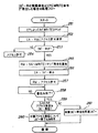
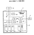
[Prior art]
The semiconductor disk device replaces the recording medium with a semiconductor memory from a magnetic disk while maintaining the behavior (command code, data transfer method, etc.) of the magnetic disk device. For this reason, the interface between the host device (CPU) and the semiconductor disk controller is exactly the same as the interface between the CPU and the magnetic disk controller. This semiconductor disk device has the advantage that it can be accessed instantly because the movement of the head is not necessary unlike the magnetic disk device, and has the advantage that the software resources between the CPU and the magnetic disk controller can be used as they are.
[0003]
FIG. 57 is a configuration diagram of such a semiconductor disk device. 1a is a CPU, 2 is a semiconductor disk device (SSD: Shared Storage Device), 3 is a semiconductor disk controller, 4 is a semiconductor disk, and a plurality of semiconductor memory modules (MS: Main Storage) 4a, 4b, 4c. 4n and a memory interface adapter (ESP: Extended Storage Adapter) 4s for controlling writing / reading of data to / from the semiconductor memory module.
In the semiconductor
[0004]
[Problems to be solved by the invention]
・ First issue
In a semiconductor disk device, a failure of a semiconductor memory module is fatal. Conventionally, when a failure occurs in a semiconductor memory module, the data is evacuated, then the power is turned off, and the failed semiconductor memory module is replaced with another semiconductor memory module. After the replacement, the power is turned on, the semiconductor disk device is started, and data is restored. However, in this method, a device for saving data is separately required, and the semiconductor disk device cannot be used when the power is turned off and when the data is saved / restored, so that there is a problem that a request for a non-stop device cannot be answered. A method of replacing a failed semiconductor memory module without stopping the semiconductor disk device has also been proposed (Japanese Unexamined Patent Publication No. 3-268020, name: Nondisruptive maintenance method for semiconductor disk). However, the proposed non-stop maintenance method for semiconductor disks has a problem that a large-scale maintenance device for enabling non-stop maintenance is required separately from the semiconductor disk device.
[0005]
・ Second task
By the way, when the power of the semiconductor disk device is turned off, its stored contents are lost. For this reason, a backup disk device may be connected to the semiconductor disk device. Each semiconductor memory module constituting the semiconductor disk is divided into a plurality of logical drives, and the higher-level device specifies a logical drive by a Start I / O command, and accesses a predetermined position of the logical drive if the logical drive is usable. It is supposed to. There is a 1: 1 relationship between the configuration of the logical drive of such a semiconductor disk and the configuration of the logical drive in the backup disk device. However, if the size or the position of the logical drive of the semiconductor disk is changed, the configuration of the logical drive between the semiconductor disk and the backup disk device does not correspond to 1: 1. Therefore, even if data is backed up to the backup disk device before the configuration of the semiconductor disk is changed, if the configuration of the logical drive of the semiconductor disk device is changed, the data backed up to the backup disk device is copied. There is a problem that the user data before the change is invalidated and cannot be used.
[0006]
・ Third issues
Since the semiconductor disk device emulates a magnetic disk device, a control information portion called a directory (DIRECTORY) is provided for each track in addition to the user data portion of the actual device. It manages addresses on the memory related to records (user data) in the track field, information on each sector, and the like.
When accessing the user data area of the specified track field, the channel adapter acquires the control information of the target track field by incorporating the directory of the specified track into the channel adapter, and stores the user data according to the information. to access. This directory is composed of (1) the record number of the last record among the records written in the track field, (2) the sector directory, and (3) the record directory. The sector directory is a table in which the number of the record which can be read first in the set sector processing is written. The record directory is a table in which a relative address (offset address) from the track head of each record is written. Yes, it is used to directly access the record field positioned by record number. By using these information, the orientation (virtual head position) can be moved directly during the set sector processing or search ID processing, and the access can be performed at high speed.
[0007]
If the target directory cannot be read due to a two-bit error in the memory or the like, all user data in the track field controlled by the directory becomes inaccessible, and effective user data is effectively lost. . For this reason, a data loss avoidance mechanism is required as a data loss avoidance mechanism that enables access to user data even when a directory falls into an unreadable state.
In a conventional semiconductor disk device, when an attempt is made to access a track field specified by the firmware of the channel adapter, first, a directory in which control information of the track field is written is read, and then normal processing is started. Therefore, if the directory cannot be read, even if an attempt is made to access the track field, access is impossible because there is no recovery means at the time of directory collapse. Therefore, in order to be able to use the unreadable track again, it is necessary to initialize the minimum directory (for example, one cylinder unit), initialize the corrupted directory, and validate the directory. However, since the initialization process causes the user data in the area to be initialized to be lost, the data in the area to be initialized must be saved in advance. Further, the data in the track field which has become inaccessible due to the collapse of the directory can be read out only by a memory dump instruction prepared as one of the channel commands. For this reason, it is impossible for anyone other than those who know the track format inside the semiconductor disk device to extract and reproduce the necessary part of the track field as user data, and it is impossible to completely restore the original data. It was almost impossible.
[0008]
・ Fourth task
In a semiconductor disk device, a data storage / storage medium is a semiconductor memory chip. Therefore, the storage cost per bit is higher than that of the magnetic disk device. Also, the storage capacity per semiconductor disk device is reduced. In order to solve the problem concerning the capacity, a method of restoring the compressed data when writing and reading the data by compressing the data has been proposed. The problem with such a compression scheme is that when rewriting user data, the size after compression may differ from the size before compression. If the data size after compression is small, it is necessary to release an extra area for effective use of memory. Conversely, if the data size after compression is large, it is necessary to secure a new area and rewrite. There is. Such memory management is complicated. Conventionally, there has been a problem that the memory area cannot be released and allocated in a simple manner while effectively using the memory.
[0009]
From aboveObject of the present inventionThe semiconductor memory module can be replaced while the semiconductor disk device is in operation without a separate maintenance device, and the access speed during replacement of the semiconductor memory module can be prevented from being reduced.Disk unitIt is to provide.
[0010]
[Means for Solving the Problems]
According to the present invention, according to the present invention, there are provided a plurality of semiconductor memory modules, a spare semiconductor memory module, a channel adapter for controlling writing and reading of data to and from the semiconductor memory module, and exclusive control for access to the semiconductor memory module. And an exclusive control unit that executes memory access, monitors a memory error in each semiconductor memory module, and accesses each semiconductor memory module by a plurality of accesses when copying the storage content of the semiconductor memory module in which the memory error occurred to a spare semiconductor memory module. A service adapter that divides the storage content of the semiconductor memory module in which a memory error has occurred in the access control unit into a spare semiconductor memory module, and that the copy has been normally completed for each predetermined unit smaller than the access control unit or not The service adapter writes information indicating whether or not the copy has been normally completed in the copy management table for each of the predetermined units, and the channel adapter refers to the copy management table when reading data. When the area to be accessed is normal, access is made. When the area is abnormal, no access is made. An error is made. When data is written, data is written in the area to be accessed, and copy management data corresponding to the area is written. Is made normal by the disk device.
[0013]
[Action]
The service adapter monitors the memory errors of each semiconductor memory module, and divides each semiconductor memory module into a plurality of access control units when copying the storage contents of the semiconductor memory module in which the memory error has occurred to the spare semiconductor memory module. Then, the storage contents of the semiconductor memory module in which a memory error has occurred in the access control unit are copied to a spare semiconductor memory module. At this time, the service adapter has a predetermined unit smaller than the access control unit. ( For example, track units ) Information indicating whether or not copying has been completed normally is written to the copy management table every time, and the channel adapter refers to the copy management table at the time of data reading, and accesses if the area to be accessed is normal, In the case of (1), an error is made without access, and at the time of data writing, data is written to the area to be accessed, and the copy management data corresponding to the area is made normal.
[0018]
【Example】
(A) First embodiment of the present invention
(A-1) Configuration of semiconductor disk device
FIG. 1 is a configuration diagram of the semiconductor disk device of the present invention. 11a-1, 11a-2,... Are CPUs (upper-level devices), 12 is a semiconductor disk device (SSD), 13 is a semiconductor disk controller, 14 is a semiconductor disk, and 15 is a service adapter (described later). This is a maintenance panel (PNL) for taking out and performing maintenance.
The
[0019]
Each semiconductor memory module is divided into a large number of ranges (
For example, a replacement procedure when an error occurs in the
(1) The storage contents of the
{Circle around (2)} After the evacuation is completed, the spare
{Circle around (3)} After the evacuation of all access control units is completed, the
[0020]
In the semiconductor
[0021]
[0022]
A storage unit (TS) 13h stores a copy management table CCT indicating success / failure (valid / invalid) of copying. The copy management table CCT manages copy success / failure in a unit of data written in the semiconductor memory module. If the copy fails (for example, if the data could not be read due to a medium error), the relevant part is invalidated. For example, as shown in FIG. 3, the success / failure of copying is managed for each track. In the case of a semiconductor disk emulating a magnetic disk, if copying is performed for each cylinder (access control unit), even if an error occurs, not all of the cylinders are invalid. Therefore, fine data can be assured by invalidating only the error track for each track by the copy management table CCT. In this case, more detailed data can be assured if the data is managed on a record basis, not on a track basis. The copy management table CCT may be located at a location where each module can refer to / update the module, and may be arranged in the semiconductor memory module.
[0023]
(A-2) Outline of first exchange control of semiconductor memory of the present invention
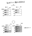
As shown in FIG. 4, the
[0024]
When a memory error occurs in the
Thereafter, copying is performed for each control unit, and when copying of all control units is completed, the contents of the control table CTL are as shown in FIG. That is, the physical addresses of all control units (ranges) for which copying has been completed are the physical addresses of the copy destination.
[0025]
(A-3) Exchange control processing of the semiconductor memory module of the present invention
・ Copy processing
FIGS. 9 and 10 are flowcharts of a copy process for copying the storage contents of the semiconductor memory module to the spare semiconductor memory module.
In response to an instruction from the maintenance panel (PNL) 15 or error detection management, the service adapter (SA) 13c recognizes a semiconductor memory module in which a memory error has occurred (
[0026]
When recognizing the semiconductor memory module in which the memory error has occurred, the service adapter SA requests the resource manager (RM) 13b to permit the use of the spare semiconductor memory module (HS) 16 (step 102). This is for confirming that the spare semiconductor memory module HS is not being used for replacing another semiconductor memory module MS. This is because, for example, when the
When the semiconductor memory module HS is in use, the resource manager RM issues a non-permission notification to the service adapter SA (
Next, the service adapter SA requests the resource manager RM to permit the use of the first access control unit of the semiconductor memory module in which the error has occurred (step 106).
[0027]
If usable, the resource manager RM notifies the service adapter SA of the use permission, and writes "the first access control unit is in use" in the exclusive control table ECT (
The service adapter SA executes the copy of the control unit according to the use permission notification (step 109). If no error occurs during copying and the copying of the access control unit is completed (
Each module changes the control table CTL of the control memory CS as instructed, and notifies the service adapter SA of the change completion (step 113). Note that the service adapter SA also changes the control table CTL of the control memory CS.
[0028]
Upon receiving the change completion notification from all the modules, the service adapter SA notifies the resource manager RM of the end of the access. As a result, the resource manager RM writes "the first access control unit has become unused" (step 114). Next, the service adapter SA checks that copying of all control units of the
When the copying of all the control units is completed, the service adapter SA notifies the host device CPU of the completion of the copying via the channel adapter CA, displays the completion of the copying on the maintenance panel PNL (step 116), and ends the copying process. When the copy processing is completed, the maintenance person replaces the semiconductor memory module (MS) 14b in which the memory error has occurred with a new semiconductor memory module.
On the other hand, if the copying of all the control units has not been completed, the copy target is changed to another control unit whose copying has not been completed (step 117), and the processing from
In
[0029]
If an error occurs in a predetermined track at the time of copying in
FIG. 11A shows a case where the copying of all the tracks of the control unit (6) succeeds without any error, and “valid” is written in the
[0030]
・ Process after semiconductor memory module replacement
FIG. 12 is a process flowchart after the semiconductor memory module is replaced.
If the maintenance staff replaces the semiconductor memory module in which the error has occurred after the copy is completed, the service adapter SA detects the completion of the replacement (step 131), and thereafter, the replaced semiconductor memory module is used as a spare semiconductor memory module (step 131). 132). After the replacement is completed, the
[0031]
・ Access processing using the copy management table
Each module refers to the copy management table CCT when reading a record from the semiconductor memory module. FIG. 14 is a processing flowchart of access with reference to the copy management table CCT.
First, it is determined whether the record is read or written (step 151). In the case of read, the validity / invalidity of the access destination track is checked by referring to the copy management table CCT (step 152). The record is read (step 153), and if invalid, error processing is performed (step 154). On the other hand, in the case of writing, if the access destination track is invalid, it is changed to "valid" (step 155), and thereafter, a record is written to the track (step 156).
[0032]
As described above, only by adding a spare semiconductor memory module, the storage contents of the semiconductor memory module in which a memory error has occurred can be evacuated without stopping, and a large-scale maintenance device is not required. In addition, since the semiconductor memory module is subdivided into access control units and copying is performed in the access control units, exclusive control can be performed in the control units. It is possible to access the control unit, and there is no adverse effect on the access of the host device.
Further, every time the copy of the access control unit is completed, the service adapter SA changes the physical address in the control table CTL provided in the channel adapter CA or the like to the physical address of the copy destination. The access control unit can immediately access the copy destination (spare semiconductor memory module).
Further, a copy management table for managing whether or not copying has been normally completed for each access control unit is provided, and a module such as the channel adapter CA refers to the copy management table at the time of data reading to access an area (track) to be accessed. If) is normal, access is made. If abnormal, access is not made and an error occurs. As a result, even if a copy error occurs during copying, erroneous data is not read and processed, and a malfunction can be prevented.
[0033]
(A-4) Outline of second exchange control of semiconductor memory of the present invention
The above is the case where the control table CTL has the configuration shown in FIG. The control table CTL may be configured as shown in FIG. The control table CTL includes (1) a logical address (CCHH), (2) an original physical address of a semiconductor disk, and (3) a physical address of a copy destination for each range (access control unit) of each semiconductor memory module. Is provided. The logical address is an address specified by the CPU or the like (for example, a cylinder / head number CCHH when specified by a data address of a magnetic disk), and the original physical address is a real address for accessing the semiconductor memory module inside the semiconductor disk device. is there. Normally, only the original physical address is associated with the logical address, and the physical address of the copy destination is invalid (control by attaching a mark, etc.).
[0034]
As shown in FIG. 4, the
[0035]
When a memory error occurs in the
Further, the service adapter SA instructs a module such as the channel adapter CA to perform a forking process when accessing the
[0036]
Thereafter, as shown in FIG. 19, the access control unit is copied. When the copying of all access control units of the
[0037]
(A-5) Exchange control of the semiconductor memory module of the present invention
・ Copy processing
FIGS. 22 and 23 are flowcharts of a copy process for copying the storage contents of the semiconductor memory module to the spare semiconductor memory module. It is assumed that the control table CTL is configured as shown in FIG.
In response to an instruction from the maintenance panel (PNL) 15 or error management, the service adapter (SA) 13c recognizes a semiconductor memory module (
When recognizing the semiconductor memory module in which the memory error has occurred, the service adapter SA requests the resource manager (RM) 13b to permit the use of the spare semiconductor memory module (HS) 16 (step 202). When the semiconductor memory module HS is in use, the resource manager RM issues a non-permission notice to the service adapter SA (
[0038]
Next, the service adapter SA instructs each module such as the channel adapter CA to start replacing the
When the completion of the change of the control table is notified from each module, the service adapter SA requests the resource manager RM to permit use of the first access control unit of the semiconductor memory module in which the error has occurred (step 208).
[0039]
If usable, the resource manager RM notifies the service adapter SA of the use permission, and writes "the first access control unit is in use" in the exclusive control table ECT (
The service adapter SA executes the copy of the control unit according to the use permission notification (step 211). If no error occurs during the copy and the copy of the access control unit is completed (
If the copying of all the control units has not been completed, the copy target is changed to another control unit whose copying has not been completed (step 216), and the processing from
In
[0040]
In
In
[0041]
Thereafter, the service adapter SA notifies the host device CPU of the end of the copy via the channel adapter CA, displays the completion of the copy on the maintenance panel PNL (step 224), and ends the copy processing. When the copy processing is completed, the maintenance person replaces the semiconductor memory module (MS) 14b in which the memory error has occurred with a new semiconductor memory module.
As described above, by simply adding a spare semiconductor memory module, the stored contents of the semiconductor memory module in which a memory error has occurred can be copied without stopping. Also, when writing data to the semiconductor memory module being copied, the channel adapter or the like writes data to two storage areas indicated by the original physical address and the copy destination physical address in accordance with the forking process. It is not necessary to change the control table every time the copy of the control unit is completed as in the case of the first exchange control process.
[0042]
• Processing when a write instruction is issued to the control unit area being copied
In some cases, a write command is issued from the host device CPU to the control unit area being copied. In such a case, the write command can be made to wait until the copy is completed, but the access speed of the host device is reduced. Therefore, control is performed such that copying is temporarily stopped with priority given to the write command. FIG. 24 is a flowchart of a process when a write command is issued to the control unit area during such copying.
When a write command is issued from the host device CPU to the channel adapter CA (step 251), the channel adapter requests access permission to the resource manager RM for the access control unit (step 252). The resource manager checks whether the access control unit is being copied, and if not, notifies the channel adapter CA of access permission (
[0043]
On the other hand, if copying is in progress, the
When the writing by the channel adapter CA is completed (step 258), the service adapter SA compares the write access unit (the number of tracks = Aw) with the copy access unit (the number of tracks = Ac, for example, Ac = 1). (Step 259).
If Aw ≧ Ac, the service adapter SA considers that copying has been completed for the access unit of the write command (step 260), and resumes copying for the remaining portion thereafter.
[0044]
On the other hand, if Aw <Ac, the copy unit including the access unit of the write command is copied again assuming that the copy has not been completed, or the copy unit other than the access unit is copied (step 261) Then, copying is resumed for the remaining portion.
As described above, since the copy is stopped and the write command of the host device CPU is executed, the access speed of the host device does not decrease. When the access unit is larger than the copy unit, the copy of the access unit can be regarded as completed and the copy speed can be improved.
[0045]
(A-6) Actual configuration of the semiconductor disk device
FIG. 25 is an overall configuration diagram of a semiconductor disk device, which has a duplex configuration, wherein a module having a
The CA is a channel adapter that controls the interface with the channel of the host device, and various channel adapters corresponding to an electric channel, an optical channel, and an OC link are appropriately connected. An RM is a resource manager that controls processing operations such as exclusive control and logical path management, and performs resource management of the entire subsystem. SA is a service adapter, which becomes a master and manages the status of other units (modules).
[0046]
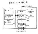
C-BUS is a control bus for each unit to access message communication and control information, D-BUS is a data transfer bus for each unit to exchange data with the semiconductor disk, and S-BUS is a master for the service module. The service bus manages the status of each unit. BH-1 and BH-2 are bus handlers for controlling bus contention and distributing a bus clock, MDK is a magnetic disk device (optional) for temporarily backing up the contents of the memory when a memory failure occurs, and DA is a magnetic disk device. BANK is a semiconductor disk (shared memory) for controlling the interfaces of the semiconductor memory modules MS and HS and a spare semiconductor memory module HS. ESP1 to ESP4 are ports (Extended Storage Port) for controlling access to the semiconductor disk, and ESA1 to ESA4 are memories for performing timing control between the ESP and the semiconductor memory module MS, refreshing the memory, and correcting data based on an error check code. The interface adapter and PANEL are maintenance panels.
[0047]
The first and second semiconductor disk devices G0 and G1 are configured symmetrically with respect to the center dotted line, and the upper CPU is symmetrically configured with the channel adapter CA of the first and second semiconductor disk devices.1, CA2And the respective ports ESP2 and ESP3 are connected to the other memory adapters ESA3 and ESA4. Therefore, even if a failure occurs in one channel adapter, the CPU can access the semiconductor disk from the other channel adapter. Further, even if one semiconductor disk fails, the other semiconductor disk can be accessed, thereby improving reliability.
Modules such as the channel adapter CA, the resource manager RM, and the service adapter SA are each configured by a microprocessor, and generally have a configuration shown in FIG. In the figure, 91 is a microprocessor (MPU), 92 is a control storage unit (CS) having a RAM configuration, 93 is a control storage unit (CS) having a ROM configuration, and 94 is a driver / receiver (DV / RV) connected to an internal bus. ) And 95 are bus interface logic (BIL), 96 is a driver / receiver (DV / RV) connected to an external interface, 97 is a buffer or table storage unit (TS), and 98 is an individual LSI (gate array). The number of drivers / receivers (DV / RV) 96 differs depending on the number of external interfaces connected.
[0048]
(B) Second embodiment of the present invention
(B-1) Overall configuration
When the power is turned off, the stored contents of the semiconductor disk device are lost. For this reason, a backup disk device may be connected to the semiconductor disk device.
FIG. 27 is a configuration diagram of a semiconductor disk device provided with a backup disk device, and the same parts as those in FIG. 1 are denoted by the same reference numerals. 11a-1 is a CPU (upper device), 12 is a semiconductor disk device (SSD), 13 is a semiconductor disk control device, 14 is a semiconductor disk, and 15 is a maintenance panel (PNL) for issuing various instructions to the service adapter SA to execute maintenance. ).
[0049]
The
In the
[0050]
(B-2) Logical drive configuration of semiconductor disk and magnetic disk
Each of the semiconductor memory modules (MS) 14a to 14c constituting the
FIG. 28 is a configuration diagram of a logical drive of the
[0051]
The configuration of the logical drive in the
The first configuration information table 21 indicating the configuration of the logical drive in the
[0052]
When the data stored in the
When restoring the data saved in the
[0053]
(B-3) Problems when the logical drive configuration of the
By the way, after saving the data of the
When the configuration of the
The above is the case where the size of the logical drive is changed, but the same problem occurs when the arrangement of the logical drive is changed as shown in FIG.
[0054]
(B-4) Outline of restoration processing of the present invention
FIG. 32 is a schematic explanatory diagram of the restoration processing of the present invention when the logical drive configuration of the
After the data of the
[0055]
Next, when restoration is instructed from the maintenance panel PNL, the disk adapter (DA) 19 reads the first and second configuration information tables 21 and 22 from the
Thereafter, the disk adapter DA reads the data of the i-th logical drive (i = 0 to 4) from the
After the restoration is completed, the second configuration information table 22 of the
[0056]
(B-5) Restoration processing of the present invention
FIG. 35 is a flowchart of the restoration processing of the present invention.
If it is desired to change the logical drive configuration of the
[0057]
The disk adapter DA reads the first and second configuration information tables 21 and 22 from the
[0058]
When the restoration of all data to the
As described above, even if the configuration of the semiconductor disk is changed, the data saved in the backup disk device before the configuration change can be correctly restored on the semiconductor disk device after the configuration change, and the user data before the change can be used.
[0059]
(C) Third embodiment of the present invention
(C-1) Configuration of track format, directory and count section
・ Track format
In the semiconductor disk device, a directory (control information section) is provided at the head of each track field. When accessing the user data of the designated track field, the channel adapter CA reads the directory of the track field and uses the directory to access the user data.
FIG. 36 shows an example of a track format in a semiconductor disk. A directory (DIRECTORY) is arranged at the beginning of each track, a home address (HA) is arranged thereafter, and a variable-length record (CKD) according to the CKD format follows. RECORD-0, RECORD-1,...) Are arranged. The home address HA indicates a track address (CCHH), and each record is composed of a count section C, a key section K, and a data section D.
[0060]
·directory
The directory has 448 bytes as shown in FIG. 37, (1) 1-byte last record number (LAST RECORD NO.), (2) 218-byte sector directory (SECTOR DIRECTORY), (3) 190-byte record A directory (RECORD DIRECTORY), (4) other areas such as an ID section for confirming validity, and (5) an unused area.
The last record number (LAST RECORD NO.) Indicates the record number of the last record written in the track field. An end mark (EOF) is written immediately after the last record of each track field, and the last record is the record immediately before reading the end mark. Then, the record number of the last record becomes the last record number.
[0061]
The sector directory (SECTOR DIRECTORY) stores the physical record numbers that can be read first in the set sector processing for each sector value. The physical record number is a value obtained by adding 1 to the logical record number with the home address HA set to 0. The track is divided into, for example, 218 sectors, and values of
The record directory (RECORD DIRECTORY) indicates an offset address from the head of the track to each record (
[0062]
・ Counting part
As described above, each record includes a count section C, a key section K (not necessarily required) in which a key for search is recorded, and a data section D in which user data is recorded. As shown in FIG. 38, the count section C has 64 bytes, (1) an 8-byte real data section provided from the host, and (2) a 4-byte ID section added before and after to guarantee the data. , (3) consists of a 48-byte control information section for accessing the track field. In the actual data portion, a track address (CCHH), a record number (R), a length of a subsequent key portion (KL), and a length of a data portion (DL) are recorded. In the ID part, a code for identifying the head of the record, the latest time (time stamp) at which the data was written, and the like are recorded. In the control information section, directory restoration data (control information restoration data) is recorded so that a target record can be searched even if the directory is lost, and a part of the directory can be restored. The directory restoration data includes (1) the relative address (offset address) Ai from the head of the own record to the head of the next record, and (2) the sector value Si of the sector where the own record is located.
[0063]
Since the length of the directory, the home address, and the count portion of each record is constant, the count portions of the directory, the HA, and the RECORD-0 are located at relative positions determined from the beginning of the track. As shown in FIG. 39 (a), assuming that an offset address L0 from the track head to the home address HA and an off address from the record Ri-1 are Li, these offset addresses Li (i = 0, 1, 2,...) ) Is recorded in a record directory (RECORD DIRECTORY) (see FIG. 37). In this case, assuming that the offset address from the record Ri-1 to the record Ri is Ai, the offset address Ai is recorded in the count section of the record Ri as directory restoration data. The following equation is used between Ai and Li.
Li + Ai
Is established.
[0064]
Assuming that the relationship between the sector and the record is as shown in FIG. 39 (b), 0 (HA) is changed to sector values 1-2 in correspondence with the
[0065]
(C-2) Record reading and writing procedure
FIG. 40 is an explanatory diagram of a record reading sequence of the semiconductor disk device. The semiconductor disk device has the same configuration as that of FIG.
When a seek command SK is generated from the host device CPU, the channel adapter CA immediately returns an operation end signal to the host device. Upon receiving the operation end signal, the host device CPU issues a set sector command SS. Thereafter, the upper-level device similarly issues a search ID command SID, and the channel adapter CA receives these commands.
Upon receiving the search ID command, the channel adapter CA converts the logical address (track address CCHH) specified by the seek command into a physical address of the semiconductor disk. Since this physical address indicates the head address of the track, in other words, the head address of the directory, the directory is read from the semiconductor disk.
[0066]
Next, a record number corresponding to the sector value specified by the set sector command is obtained from the sector directory (set sector operation). Thereafter, the address of the record number is obtained from the record directory, and the count part of the record is read from the address. Next, it is checked whether or not the CCHHR of the record included in the count section matches the CCHHR of the target record designated by the search ID command, and if they match, the search ID operation ends. If they do not match, the record of the next record number is read and the same processing is performed.
If the target record is found, the channel adapter CA returns an operation end signal to the host device. As a result, the host device issues a read command (READ CKD), and the channel adapter CA receives the command. Thereafter, the channel adapter CA sequentially transfers the count section C, the key section K, and the data section D to the upper-level device CPU, and finally sends a normal end to end a series of record read processing.
[0067]
FIG. 41 is an explanatory diagram of a record writing sequence of the semiconductor disk device. The procedure is the same as the record reading procedure up to the search operation.
If the target record is found by the search ID operation, the channel adapter CA returns an operation end signal to the host device. As a result, the host device issues a write command (WRITE CKD), and the channel adapter CA receives the command. Thereafter, the channel adapter CA obtains directory restoration data (control information restoration data) Ai, Si and inserts them into the counting section, and thereafter records a record.
After the record recording is completed, the channel adapter CA notifies the host device CPU that the writing has been completed. After the notification, the contents of the directory are updated and written back to the semiconductor disk position where the directory was recorded.
[0068]
(C-3) Processing when a directory reading error occurs
(1) Skip search processing
If the channel adapter CA cannot read the directory when reading or writing a record, the channel adapter CA searches for a target record (skip search) using the directory restoration data recorded in the count section of each record. Note that when the directory cannot be read, a 2-bit error occurs, an ID error occurs (write failure of the directory), and the like. When such an error occurs, the channel adapter CA cannot read the directory, You will not be able to access.
FIG. 42 is a flowchart of the skip search process when the channel adapter CA cannot read the directory, and FIG. 43 is an explanatory diagram of the skip search process.
First, the channel adapter sets 1 → i (step 401). Next, the channel adapter CA reads the count part C0 of the record Ri-1 (= R0) from the address Li-1 (= L0) (step 402). The storage position of the record R0 from the beginning of the track is fixed, and L0 is known.
[0069]
After the reading of the count section, it is checked whether the record number included in the count section is equal to the record number N instructed to access (step 403). If they are equal, the record Ri-1 is the target record, and the record is read or rewritten (step 404).
However, if the record number recorded in the count section is not equal to the record number N instructed to access, the relative address (offset address) Ai to the next record Ri recorded in the count section is obtained (step 405). ).
Then,
Li-1 + Ai → Li
Then, the offset address Li from the beginning of the track of the record Ri is calculated (step 406). After the Li calculation, i is incremented (i + 1 → i, step 407). As described above, the record number recorded in the count section in
In this way, even if a directory cannot be read when reading or writing a record specified by the host device CPU, the channel adapter CA automatically uses the directory restoration data recorded in each record to read the host device. It is possible to search for a designated target record and read or write the record.
[0070]
(2) Rebuild directory
When the directory cannot be read, the target record can be searched by the skip search method. In this case, the directory can be reconstructed using the directory restoration data in parallel with the skip search processing.
・ Record directory reorganization processing
FIG. 44 is a flowchart showing the process of reconstructing the record directory.
First, L0 and L1 (fixed values) are set in the record directory as the home address HA and the offset address of the record R0 (step 421). Thereafter, i is set to 1 and the count part of the record Ri-1 is read (
Next, it is checked whether the read information is an end mark (EOF) (step 424). If the information is not EOF, a relative address (offset address) Ai to the next record Ri is obtained from the counting section (step 425).
[0071]
If Ai is found, the following equation
Li-1 + Ai → Li
Then, the offset address Li from the track head of the record Ri is calculated (step 426). Next, Li is set in the record directory as an offset address from the top of the record Ri (step 427), i is incremented (i + 1 → i, step 428), and the processing of
If the above process is repeated, sometime in
Thus, the record directory can be restored.
[0072]
・ Sector directory reconfiguration processing
FIG. 45 is a flowchart showing the process of reconstructing the sector directory.
The home address HA and the position of the count part of the record R0 are fixed. Therefore, H0 and R0 are set corresponding to the first several sector values in the sector directory (step 451).
Next, i is set to 1 and the count part of the record Ri-1 is read (
[0073]
If Ai is found, the following equation
Li-1 + Ai → Li
Calculates the offset address Li from the track head of the record Ri (step 455). Next, the count part of the record Ri is read (step 456), and it is checked whether the read information is an end mark (EOF) (step 457). If it is not EOF, the leading sector value Si of the record Ri is obtained from the count part of the record Ri (step 458). Next, a record Ri is written in correspondence with the sector value Si in the sector directory (step 459). Thereafter, i is incremented (i + 1 → i, step 460), and the processing from
[0074]
If the above process is repeated, sometime in
In this way, the channel adapter CA automatically uses the directory restoration data to read the directory even if an error that prevents the directory from being read occurs when reading or writing the record specified by the host device CPU. Since the rebuilding is performed, the directory can be referred to at the time of the next access, and high-speed access can be performed.
[0075]
FIG. 46 is an explanatory diagram of an overall schematic sequence when an error occurs in a directory. When a record read command READ D is issued from the host device (host) CPU, the channel adapter CA accepts the command and performs a directory read process. When a directory reading error occurs, the channel adapter CA switches the access method from the normal directory use access method to the skip search method. Thereafter, the target record is skip-searched according to the procedure shown in FIG. 42, and when the target record is found, the data portion is transferred to the higher-level device. In this case, the directory can be reconstructed by performing the reconstruction process of the record directory and the sector directory shown in FIGS. 44 and 45 in parallel with the skip search process.
[0076]
(C-4) Another processing when an error occurs in the directory
In the above, a description has been given of a case where, when an error occurs in a directory, a target record is automatically searched and read / written, and the directory is reconstructed. However, the search for the target record and the reconstruction of the directory may be performed in accordance with an instruction from the host device CPU.
FIG. 47 is an explanatory diagram of a record read procedure in such a case.
When a record read command READ CKD is issued from the host device (host) CPU, the channel adapter CA receives the command and performs a directory read process. In this case, when a directory reading error occurs, the channel adapter CA creates error information and reports the error to the host device.
[0077]
The host CPU analyzes the error and issues a special dump command and a record number N to the channel adapter CA. The channel adapter CA accepts the special dump command, searches for a target record in accordance with the procedure shown in FIG. 42, and when the target record is obtained, sequentially transfers the count unit, the key unit, and the data unit to the host device.
The above is the case where the processing by the special dump instruction does not accompany the directory reconstruction processing. When the directory rebuilding process is involved, the record directory and the sector directory shown in FIGS. 44 and 45 are rebuilt, the directory is rebuilt, and the data is written at the head of the target track.
[0078]
(C-5) Processing when a directory error occurs during copying
When a memory failure occurs in the semiconductor disk device, the contents of the semiconductor memory module MS in which the error has occurred are copied to the spare semiconductor memory module HS under the control of the service adapter SA, and then the failed semiconductor memory module is replaced with a new one. Replace with a semiconductor memory module (first embodiment, see FIG. 1).
In such a case, the service adapter SA performs copying other than the track in which the error has occurred, and requests the channel adapter CA to copy the track field in which the error has occurred.
This is because the service adapter SA cannot perform processing in units of fields, and performs block copying for each fixed length (64 bytes). For this reason, even if a similar copy process is performed on the copy of the track field in which an error has occurred, the error occurrence information cannot be written in the directory or the additional information of each count unit, and access to user data cannot be guaranteed. is there. Therefore, the service adapter SA requests the channel adapter CA for the copy processing of the track field in which the memory failure has occurred, and the requested channel adapter CA performs the copy processing in order from the directory to the end mark EOF in field units.
[0079]
If the channel adapter CA finds a field (counting part, key part, data part) that causes a memory failure in the middle of copying, it invalidates only that field (in the case of the counting part, the entire record) and necessitates the counting part. Rewrite the control information. However, if the directory is invalidated when a memory failure occurs in the directory, all records on the track field are invalidated. Further, since the channel adapter CA cannot read the directory, the format of the track is changed. I can't judge.
[0080]
In order to avoid this, the channel adapter CA copies the HA field at the fixed position and the record R0, and copies the fields after the record R1 to the end mark while acquiring the address of the next record field by the skip search method. I do. That is, if the count part of the current record is read, the offset address to the next record necessary for reconstructing the directory, the sector value of the current record, the key length of the current record, and the data length can be obtained, and a copy of the current record field can be obtained. Go to the next record. If this is continued until the end mark is detected, all fields except the directory can be copied. Further, since the copy process includes a process of reading the directory restoration data of all the record parts necessary for the directory reconstruction, the directory can be necessarily reconstructed. Therefore, the directory rebuilding process is performed at the same time as the copying process of each field, and the directory rebuilt in the channel adapter CA is written to the copy destination directory area, thereby preventing the loss of user data during the memory exchange process. be able to.
[0081]
FIG. 48 and FIG. 49 are flowcharts of copy processing when an error occurs in the semiconductor memory. It is assumed that the semiconductor disk device has the configuration shown in FIG.
When recognizing the semiconductor memory module MS and the track in which the error has occurred (step 501), the service adapter SA starts copying the semiconductor memory module MS (step 502).
It is checked whether the track to be copied is an error track (step 503). If the track is not an error track, copying of the track is executed (step 504). After the copy is completed, it is checked that the copy of the semiconductor memory module MS is completed (step 504). Step 505), if completed, perform the processing from
[0082]
On the other hand, if the track to be copied is an error track in
If there is no error in the field in
[0083]
Thereafter, it is checked that the end mark EOF has been detected (step 515), and if not detected, the process jumps to step 507 to copy the subsequent fields.
If the end mark EOF is detected, it is checked whether F = "1" (step 516), and if F = "0", the copy completion is notified to the service adapter SA (step 517). As a result, the service adapter repeats the copy processing from
In
[0084]
As described above, according to the third embodiment, even if the directory cannot be read, access to the target record specified by the higher-level device using the control information restoration data included in each record without using the directory is performed. It becomes possible. Further, since the directory can be reconstructed using the control information restoration data, access can be made using the reconstructed directory. Therefore, the access speed does not decrease.
In addition, even if an error that makes it impossible to read the directory is detected in the copy processing when replacing the semiconductor memory module due to a memory error, the next record position is sequentially determined using the control information restoration data included in each record. Can be copied, and the directory can be reconstructed and written to the copy destination directory area.
[0085]
(D) Fourth embodiment
(D-1) Overall configuration
FIG. 50 is a configuration diagram of an embodiment of a semiconductor disk device that compresses data and stores the data on a semiconductor disk. The semiconductor disk device has a duplex configuration, and a module having a
[0086]
CA1, CA2Is a channel adapter that controls the interface with the CPU and channel of the host device, and is connected to the host device (channel). RM1, RM2Is a resource manager, which controls processing operations such as exclusive control and performs resource management of the entire subsystem. TS1, TS2Is a table storage (table storage unit) for storing tables such as an exclusive control table, and SA1, SA2Is a service adapter, MDK is a magnetic disk device for temporarily backing up the contents of a semiconductor disk, DA1, DA2Is a device adapter that controls the interface with the magnetic disk drive, BANK1, BANK2Is a semiconductor disk on which a plurality of semiconductor memory modules and spare semiconductor memory modules are mounted. ESP1, ESP2Is a port for controlling access to the semiconductor disk, MT1, MT2Is a semiconductor memory table for storing the used / unused state of each block when the semiconductor memory is divided into a plurality of blocks of a predetermined size;1, MCA2Manages the used / unused state of each block in the semiconductor memory, and uses the channel adapter CA1, CA2An unused block is allocated in response to a block request from, and the block is used, and a predetermined used block is changed to unused in response to a block release request from the channel adapter.
[0087]
BUS1, BUS2Is a bus having a control bus, a data transfer bus, and a service bus. CBUS is one table storage unit TS1(TS2) Changes immediately, the other table storage unit TS2(TS1) Is copied to one of the semiconductor memory tables MT.1(MT2) Changes immediately, the other semiconductor memory table MT2(MT1) Is a copy bus for copying.
The first and second semiconductor disk devices G0 and G1 are configured symmetrically with respect to the center dotted line, and the upper CPU is symmetrically configured with the channel adapter CA of the first and second semiconductor disk devices.1, CA2It is connected to the.
[0088]
(D-2) Configuration of semiconductor memory
As shown in FIG. 51, the semiconductor memory BANK is divided into a track emulation area 51 and a compressed data storage area 52 for compressing and storing a data portion of a record. The compressed data storage area 52 is divided into a large number of blocks (logical blocks) of a predetermined size, and after the data portion of each record is compressed, it is stored in a required number of blocks continuously or dispersedly.
[0089]
Each track in the track emulation area 51 has the track format shown in FIG. 36 except that the data part of the record is not stored. As shown in FIG. 52, each track field stores a directory, a home address HA, a count portion and a data portion of
To write a record, as shown in FIG. 53, the data portion DT of the record to be written is compressed into compressed data DT ', and then a number of blocks (three in the figure) corresponding to the size of the compressed data DT' The first to third portions (1) to (3) of the compressed data DT 'are stored in the secured blocks B1 to B3, and the block addresses of these blocks B1 to B3 are inserted into the count section to perform track emulation. It is stored in the area 51.
[0090]
(D-3) Configuration of channel adapter
FIG. 54 is a configuration diagram of a channel adapter that performs compression / decoding processing. Inside the channel adapter, 61 is a large-capacity (for example, one track) first data buffer for storing uncompressed data, 62 is a large-capacity (for example, one track) second data buffer for storing compressed data, 63 Is a data compression mechanism for compressing / decoding data, 64 is a dictionary memory for assisting the compression / decoding operation, 64 is a channel interface protocol controller, and 65 is a selector for selecting data from the first and second data buffers. A
[0091]
(D-4) Record reading processing
FIG. 55 is a sequence explanatory diagram of the record reading process.
When a seek command SK is generated from the host device CPU, the channel adapter CA (MPU 69) immediately returns an operation end signal to the host device. Upon receiving the operation end signal, the host device CPU issues a set sector command SS. Thereafter, the upper device issues a search ID command SID and a read command (READ CKD) in the same manner, and the channel adapter CA receives these commands.
When receiving the read command, the
[0092]
Next, a record number corresponding to the sector value specified by the set sector command is obtained from the sector directory (set sector operation). Thereafter, the address of the record number is obtained from the record directory, the count part of the record is read from the address, and the CCHHR of the record included in the count part matches the CCHHR of the target record specified by the search ID command. To check. If they match, the search ID operation ends. If they do not match, the record of the next record number is read and the same processing is performed.
When the target record is found, the count section C and key section K of the record are read out via the internal bus interface control section (BIL) 66. The
[0093]
(D-5) Record rewriting process
FIG. 56 is a flowchart of the record rewriting process. Until a write command (WRITE D) is received, the process is the same as that of the read command.
When receiving the write command (WRITE D) from the higher-level device, the channel
[0094]
Thereafter, as in the case of the read command, the address of the target record is obtained, and the count section of the target record is read from the address (step 603). Then, the block address and the number of blocks Bo included in the counting section are stored (step 604). The block address and the number of blocks indicate the address of the block in which the data part of the target record is stored and the number thereof.
When the storage of the block address and the number of blocks Bo is completed, or in parallel with the above, the
If the number of blocks Bn is obtained, the size of the block is compared with the number of blocks Bo so far (step 607). If Bn = Bo, the current block address is set in BIL (step 608). Write the compressed data to the block designated by (1) (step 609).
[0095]
On the other hand, if Bn <Bo, the
[0096]
If Bn> Bo, the
[0097]
As described above, according to the fourth embodiment, the user data is compressed and stored, so that the memory can be effectively used. Further, since the control information (directory, count unit, etc.) is not compressed, the restoration processing is not required, and the host Data access time can be reduced. According to the fourth embodiment, when data is compressed and written into the semiconductor memory, the memory area can be effectively released and allocated to effectively use the memory.
As described above, the present invention has been described with reference to the embodiments. However, the present invention can be variously modified in accordance with the gist of the present invention described in claims, and the present invention does not exclude these.
[0098]
【The invention's effect】
According to the present inventionBy simply adding a spare semiconductor memory module, the stored contents of the semiconductor memory module in which a memory error has occurred can be evacuated without stopping, and a large-scale maintenance device is not required.
Also,The present inventionAccording to this, the semiconductor memory module is subdivided into access control units, and copying is performed in the access control units. Therefore, exclusive control can be performed in the control unit, and even during copying, the host device can access another access control unit portion that is not a copy target, which may adversely affect the access of the host device. Absent.
Furthermore,The present inventionAccording to this, each time the copy of the control unit is completed, the service adapter SA changes the physical address in the control table CTL provided in the channel adapter CA or the like to the physical address of the copy destination. After completion, the access control unit can immediately access the copy destination (spare semiconductor memory module).
[0099]
Also,The present inventionAccording to the above, a copy management table for managing whether or not copying has been normally completed for each access control unit is provided, and a module such as the channel adapter CA refers to the copy management table at the time of data reading, and specifies an area to be accessed. If the (track) is normal, access is made. If it is abnormal, access is not made and an error occurs. As a result, even if a copy error occurs during copying, erroneous data is not read and processed, and a malfunction can be prevented.
FurtherThe present inventionAccording to this, when writing data to a semiconductor memory module being copied, a module such as a channel adapter writes data to two storage areas indicated by an original physical address and a copy destination physical address according to forking processing. As a result, it is not necessary to change the control table every time the control unit is copied, and the copy can be performed at high speed.
or,The present inventionAccording to the method described above, since the copy is stopped and the write command of the host device CPU is executed, the access speed of the host device does not decrease. In this case, if the access unit is larger than the copy unit, it is considered that the copy of the access unit has been completed, so that the copy speed can be improved.
[Brief description of the drawings]
FIG. 1 is a configuration diagram (first embodiment) of a semiconductor disk device of the present invention.
FIG. 2 is an explanatory diagram of a control table.
FIG. 3 is an explanatory diagram of a copy management table.
FIG. 4 is a configuration diagram of a semiconductor disk.
FIG. 5 is an explanatory diagram of the contents (initial state) of a control table.
FIG. 6 is an explanatory diagram of a copy process.
FIG. 7 is an explanatory diagram of the contents (intermediate) of a control table.
FIG. 8 is an explanatory diagram of the contents (copy completed) of a control table.
FIG. 9 is a flowchart (part 1) of a copy process;
FIG. 10 is a flowchart (part 2) of a copy process;
FIG. 11 is an explanatory diagram of a copy management table.
FIG. 12 is a processing flowchart after replacement of a semiconductor memory module.
FIG. 13 is another processing flowchart after replacement of the semiconductor memory module;
FIG. 14 is a flowchart of an access process using a copy management table.
FIG. 15 is another configuration diagram of the control table.
FIG. 16 is an explanatory diagram of the contents (at the initial stage) of a control table.
FIG. 17 is an explanatory diagram of the contents of a control table (after a change instruction).
FIG. 18 is an explanatory diagram of a forking process.
FIG. 19 is an explanatory diagram of a copy process.
FIG. 20 is an explanatory diagram of the contents of a control table (after a physical address exchange instruction).
FIG. 21 is an explanatory diagram of the contents of a control table (at the end of copying).
FIG. 22 is a flowchart (part 1) of a copy process.
FIG. 23 is a flowchart (part 2) of a copy process;
FIG. 24 is a processing flowchart when a write instruction is issued to a control unit area being copied;
FIG. 25 is an actual configuration diagram of a semiconductor disk device.
FIG. 26 is a configuration diagram of each module.
FIG. 27 is another configuration diagram (second embodiment) of the semiconductor disk device of the present invention.
FIG. 28 shows the configuration of a logical drive.
FIG. 29 is an explanatory diagram of a change in a logical drive configuration.
FIG. 30 is an explanatory diagram of a conventional problem at the time of changing a logical drive.
FIG. 31 is another explanatory diagram of a logical drive configuration change.
FIG. 32 is a schematic explanatory diagram of the restoration processing of the present invention.
FIG. 33 is an explanatory diagram of an address conversion table.
FIG. 34 is an explanatory diagram of restoring user data.
FIG. 35 is a flowchart of a restoration process according to the present invention.
FIG. 36 is an explanatory diagram of a track format in a semiconductor disk.
FIG. 37 is a configuration diagram of a directory.
FIG. 38 is a configuration diagram of a counting unit.
FIG. 39 is a diagram illustrating the configuration of a track field.
FIG. 40 is an explanatory diagram of a record reading sequence.
FIG. 41 is an explanatory diagram of a record writing sequence.
FIG. 42 is a flowchart of a skip search process using counting unit additional information.
FIG. 43 is an explanatory diagram of a skip search process using counting unit additional information.
FIG. 44 is a flowchart of a record directory restructuring process.
FIG. 45 is a flowchart of a process of reconstructing a sector directory.
FIG. 46 is an explanatory diagram of an entire sequence when an error occurs in a directory.
FIG. 47 is an explanatory diagram of host access using the track special access method.
FIG. 48 is a flowchart (part 1) of a copy process performed when an error occurs in a semiconductor memory;
FIG. 49 is a flowchart (part 2) of a copy process performed when an error occurs in the semiconductor memory;
FIG. 50 is a configuration diagram (fourth embodiment) of a semiconductor disk device.
FIG. 51 is an explanatory diagram of a memory map.
FIG. 52 is an explanatory diagram of a track emulation area.
FIG. 53 is an explanatory diagram of storing user data in a logical block;
FIG. 54 is a configuration diagram of a channel adapter.
FIG. 55 is an explanatory diagram of a record reading sequence.
FIG. 56 is a flowchart of a record rewriting process.
FIG. 57 is a configuration diagram of a conventional semiconductor disk device.
[Explanation of symbols]
11a-1, 11a-2 ··· Host device
12. Semiconductor disk device
13. Semiconductor disk controller
13a-1, 13a-2 channel adapter
13b ・ ・ Resource manager
13c Service adapter
14. Semiconductor disk
14a to 14n ··· A plurality of semiconductor memory modules
16. Spare semiconductor memory module
Claims (7)
予備の半導体メモリモジュールと、
半導体メモリモジュールへのデータの書き込み及び読み出しを制御するチャネルアダプタと、
半導体メモリモジュールへのアクセスに関して排他制御を実行する排他制御部と、
各半導体メモリモジュールのメモリエラーを監視し、メモリエラーが発生した半導体メモリモジュールの記憶内容を予備の半導体メモリモジュールにコピーする際、各半導体メモリモジュールをそれぞれ複数のアクセス制御単位に分け、該アクセス制御単位でメモリエラーが生じた半導体メモリモジュールの記憶内容を予備の半導体メモリモジュールにコピーするサービスアダプタと、
前記アクセス制御単位より小さい所定単位毎にコピーが正常に完了したか否かを示すコピー管理テーブル、
を備え、サービスアダプタは、コピーが正常に完了したか否かを示す情報を前記所定単位毎に前記コピー管理テーブルに書込み、
前記チャネルアダプタはデータリード時に該コピー管理テーブルを参照し、アクセス対象である領域が正常の場合にはアクセスし、異常の場合にはアクセスせずエラーとし、又、データライト時、アクセス対象の領域にデータを書き込むと共に、該領域に応じたコピー管理データを正常とすることを特徴とするディスク装置。 A plurality of semiconductor memory modules;
A spare semiconductor memory module;
A channel adapter that controls writing and reading of data to and from the semiconductor memory module;
An exclusive control unit that performs exclusive control on access to the semiconductor memory module;
When monitoring the memory error of each semiconductor memory module and copying the storage contents of the semiconductor memory module in which the memory error has occurred to the spare semiconductor memory module , each semiconductor memory module is divided into a plurality of access control units, and the access control is performed. A service adapter for copying the storage content of the semiconductor memory module in which a memory error has occurred in units to a spare semiconductor memory module;
A copy management table indicating whether copying has been completed normally for each predetermined unit smaller than the access control unit,
The service adapter writes information indicating whether or not the copy has been normally completed in the copy management table for each of the predetermined units,
The channel adapter refers to the copy management table at the time of data reading, accesses when the area to be accessed is normal, makes an error without accessing when the area is abnormal, and sets the area to be accessed at the time of data writing. A disk device for writing data to the disk and normalizing copy management data corresponding to the area.
前記サービスアダプタはアクセス制御単位のコピー完了後に、該制御テーブルにおけるアクセス制御単位の物理アドレスをコピー先の物理アドレスに変更するように制御する、
ことを特徴とする請求項1又は請求項2記載のディスク装置。 At least the channel adapter is provided with a control table for holding a correspondence between logical addresses and physical addresses for each access control unit of each semiconductor memory module,
The service adapter after the completion copy of the access control unit performs control to change the physical address of the access control unit in the control table to the destination physical address,
3. The disk device according to claim 1, wherein:
予備の半導体メモリモジュールと、 A spare semiconductor memory module;
半導体メモリモジュールへのデータの書き込み及び読み出しを制御するチャネルアダプタと、 A channel adapter that controls writing and reading of data to and from the semiconductor memory module;
半導体メモリモジュールへのアクセスに関して排他制御を実行する排他制御部と、 An exclusive control unit that performs exclusive control on access to the semiconductor memory module;
各半導体メモリモジュールのメモリエラーを監視し、メモリエラーが発生した半導体メモリモジュールの記憶内容を予備の半導体メモリモジュールにコピーする際、各半導体メモリモジュールをそれぞれ複数のアクセス制御単位に分け、該アクセス制御単位でメモリエラーが生じた半導体メモリモジュールの記憶内容を予備の半導体メモリモジュールにコピーするサービスアダプタ、 When monitoring the memory error of each semiconductor memory module and copying the storage contents of the semiconductor memory module in which the memory error has occurred to the spare semiconductor memory module, each semiconductor memory module is divided into a plurality of access control units, and the access control is performed. A service adapter for copying the storage content of a semiconductor memory module in which a memory error has occurred in units to a spare semiconductor memory module,
を備え、少なくとも前記チャネルアダプタは、各半導体メモリモジュールのアクセス制御単位毎に論理アドレスと物理アドレスの対応を保持する制御テーブルを備え、 At least, the channel adapter includes a control table that holds a correspondence between a logical address and a physical address for each access control unit of each semiconductor memory module,
メモリエラーが発生して半導体メモリモジュールの記憶内容を予備の半導体メモリモジュールにコピーするに先だって、前記サービスアダプタは、エラーが生じた半導体メモリモジュールの各論理アドレスにオリジナルな物理アドレスとコピー先の物理アドレスとが対応するように前記制御テーブルを変更すると共に、前記チャネルアダプタに該半導体メモリモジュールへのデータ書き込みをオリジナルな物理アドレスとコピー先の物理アドレスが示す2つの記憶エリアに書き込むように指示し、エラーが生じた半導体メモリモジュールの予備の半導体メモリモジュールへのコピー終了後に、エラーが生じた半導体メモリモジュールの各論理アドレスに前記コピー先の物理アドレスのみが対応するように前記制御テーブルを変更することを特徴とするディスク装置。 Prior to copying the storage contents of the semiconductor memory module to the spare semiconductor memory module due to the occurrence of the memory error, the service adapter assigns the original physical address and the physical address of the copy destination to each logical address of the semiconductor memory module in which the error occurred. The control table is changed so that the addresses correspond to each other, and the channel adapter is instructed to write data to the semiconductor memory module into two storage areas indicated by the original physical address and the copy destination physical address. After the copying of the semiconductor memory module with the error to the spare semiconductor memory module is completed, the control table is changed so that only the physical address of the copy destination corresponds to each logical address of the semiconductor memory module with the error. Specially Disk apparatus according to.
該排他制御部はライト命令の対象である領域がコピー中の場合には、前記サービスアダプタにライト命令の発生を通知し、
該サービスアダプタは該通知によりコピーを停止し、
前記チャネルアダプタは該領域にデータを書き込むことを特徴とする請求項4記載のディスク装置。 The channel adapter when receiving a write command from the host device to request permission to the exclusive control unit,
The exclusive control unit when the region is the subject of the write instruction is being copied notifies the occurrence of the write command to the service adapter,
The service adapter stops copying according to the notification,
5. The disk device according to claim 4, wherein the channel adapter writes data to the area .
Priority Applications (4)
| Application Number | Priority Date | Filing Date | Title |
|---|---|---|---|
| JP10392794A JP3561002B2 (en) | 1994-05-18 | 1994-05-18 | Disk unit |
| US08/408,911 US5859960A (en) | 1994-05-18 | 1995-03-22 | Semiconductor disk apparatus having a semiconductor memory for a recording medium |
| KR1019950010336A KR100226211B1 (en) | 1994-05-18 | 1995-04-28 | Semiconductor disk device |
| DE19515661A DE19515661C2 (en) | 1994-05-18 | 1995-04-28 | Semiconductor disk device |
Applications Claiming Priority (1)
| Application Number | Priority Date | Filing Date | Title |
|---|---|---|---|
| JP10392794A JP3561002B2 (en) | 1994-05-18 | 1994-05-18 | Disk unit |
Related Child Applications (3)
| Application Number | Title | Priority Date | Filing Date |
|---|---|---|---|
| JP2004039124A Division JP2004199711A (en) | 2004-02-17 | 2004-02-17 | Semiconductor disk drive |
| JP2004039126A Division JP2004158047A (en) | 2004-02-17 | 2004-02-17 | Semiconductor disk drive |
| JP2004039125A Division JP2004213684A (en) | 2004-02-17 | 2004-02-17 | Semiconductor disk drive |
Publications (2)
| Publication Number | Publication Date |
|---|---|
| JPH07311661A JPH07311661A (en) | 1995-11-28 |
| JP3561002B2 true JP3561002B2 (en) | 2004-09-02 |
Family
ID=14367071
Family Applications (1)
| Application Number | Title | Priority Date | Filing Date |
|---|---|---|---|
| JP10392794A Expired - Fee Related JP3561002B2 (en) | 1994-05-18 | 1994-05-18 | Disk unit |
Country Status (4)
| Country | Link |
|---|---|
| US (1) | US5859960A (en) |
| JP (1) | JP3561002B2 (en) |
| KR (1) | KR100226211B1 (en) |
| DE (1) | DE19515661C2 (en) |
Cited By (1)
| Publication number | Priority date | Publication date | Assignee | Title |
|---|---|---|---|---|
| EP2704050A1 (en) * | 2012-08-31 | 2014-03-05 | Fujitsu Limited | Capacity on Demand processing apparatus and control method |
Families Citing this family (22)
| Publication number | Priority date | Publication date | Assignee | Title |
|---|---|---|---|---|
| JP3948692B2 (en) * | 1999-03-26 | 2007-07-25 | シャープ株式会社 | Semiconductor memory device |
| US6542980B1 (en) * | 2000-08-11 | 2003-04-01 | Trw Inc. | Time slot data memory storage and access system |
| US7433948B2 (en) | 2002-01-23 | 2008-10-07 | Cisco Technology, Inc. | Methods and apparatus for implementing virtualization of storage within a storage area network |
| US7934023B2 (en) | 2003-12-01 | 2011-04-26 | Cisco Technology, Inc. | Apparatus and method for performing fast fibre channel write operations over relatively high latency networks |
| US7406624B2 (en) * | 2005-02-15 | 2008-07-29 | General Motors Corporation | Method for responding to a control module failure |
| US20070005625A1 (en) * | 2005-07-01 | 2007-01-04 | Nec Laboratories America, Inc. | Storage architecture for embedded systems |
| US8886892B2 (en) * | 2007-01-26 | 2014-11-11 | Hewlett-Packard Development Company, L.P. | Memory module and method employing a multiplexer to replace a memory device |
| JP5014821B2 (en) * | 2007-02-06 | 2012-08-29 | 株式会社日立製作所 | Storage system and control method thereof |
| JP5224800B2 (en) * | 2007-12-21 | 2013-07-03 | 株式会社東芝 | Information processing apparatus and data recovery method |
| US8041991B2 (en) * | 2008-11-18 | 2011-10-18 | Lsi Corporation | System and method for recovering solid state drive data |
| US8239724B2 (en) * | 2009-04-08 | 2012-08-07 | Google Inc. | Error correction for a data storage device |
| US8447918B2 (en) | 2009-04-08 | 2013-05-21 | Google Inc. | Garbage collection for failure prediction and repartitioning |
| JP4836014B2 (en) * | 2009-07-24 | 2011-12-14 | 日本電気株式会社 | Disk array device and physical disk restoration method |
| EP2467855A4 (en) * | 2009-08-21 | 2013-08-21 | Rambus Inc | In-situ memory annealing |
| WO2012098633A1 (en) * | 2011-01-17 | 2012-07-26 | 富士通株式会社 | Memory management method, memory management device and memory management circuit |
| US9513845B2 (en) | 2012-03-30 | 2016-12-06 | Violin Memory Inc. | Memory module virtualization |
| JP5949408B2 (en) * | 2012-10-02 | 2016-07-06 | 富士通株式会社 | Information processing apparatus, information processing apparatus control method, and information processing apparatus control program |
| US20150269092A1 (en) | 2014-03-19 | 2015-09-24 | Fujitsu Limited | Information processing device and shared memory management method |
| US10067833B2 (en) | 2014-07-31 | 2018-09-04 | Hitachi, Ltd. | Storage system |
| JP6406027B2 (en) | 2015-01-20 | 2018-10-17 | 富士通株式会社 | Information processing system, information processing apparatus, and memory access control method |
| JP7213712B2 (en) * | 2019-02-14 | 2023-01-27 | キオクシア株式会社 | Nonvolatile semiconductor memory device |
| EP4300319A4 (en) * | 2022-05-18 | 2024-02-28 | Changxin Memory Technologies, Inc. | HOT PLUGGING METHOD AND APPARATUS FOR MEMORY MODULE, AND MEMORY MODULE |
Family Cites Families (22)
| Publication number | Priority date | Publication date | Assignee | Title |
|---|---|---|---|---|
| US4148098A (en) * | 1976-10-18 | 1979-04-03 | Xerox Corporation | Data transfer system with disk command verification apparatus |
| US4244049A (en) * | 1979-02-02 | 1981-01-06 | Burroughs Corporation | Method and apparatus for enhancing I/O transfers in a named data processing system |
| US4630030A (en) * | 1984-06-28 | 1986-12-16 | Wang Laboratories, Inc. | Compression of data for storage |
| JPH0673101B2 (en) * | 1984-12-26 | 1994-09-14 | 富士通株式会社 | Semiconductor disk device |
| JPS61201356A (en) * | 1985-03-01 | 1986-09-06 | Nippon Telegr & Teleph Corp <Ntt> | Memory device |
| JPS6219953A (en) * | 1985-07-17 | 1987-01-28 | Fujitsu Ltd | Recognizing system for packaged storage capacity |
| US4754396A (en) * | 1986-03-28 | 1988-06-28 | Tandem Computers Incorporated | Overlapped control store |
| DE3612730A1 (en) * | 1986-04-16 | 1987-10-22 | Ant Nachrichtentech | Processor system |
| JPS62260223A (en) * | 1986-05-06 | 1987-11-12 | Mitsubishi Electric Corp | Data mutual transfer control device |
| US4870643A (en) * | 1987-11-06 | 1989-09-26 | Micropolis Corporation | Parallel drive array storage system |
| JPH0267623A (en) * | 1988-09-01 | 1990-03-07 | Fujitsu Ltd | Directory reproducing system for semiconductor disk device |
| JPH0277927A (en) * | 1988-09-14 | 1990-03-19 | Hitachi Ltd | Control system for semiconductor disk subsystem |
| GB8915875D0 (en) * | 1989-07-11 | 1989-08-31 | Intelligence Quotient United K | A method of operating a data processing system |
| JPH03136169A (en) * | 1989-10-23 | 1991-06-10 | Nec Corp | Electronic filing device |
| US5276867A (en) * | 1989-12-19 | 1994-01-04 | Epoch Systems, Inc. | Digital data storage system with improved data migration |
| JPH03268020A (en) * | 1990-03-19 | 1991-11-28 | Hitachi Ltd | Non-stop maintenance system for semiconductor disk |
| JPH04217017A (en) * | 1990-12-19 | 1992-08-07 | Fujitsu Ltd | Memory extension method for semiconductor disk device |
| JPH04338815A (en) * | 1991-05-16 | 1992-11-26 | Fujitsu Ltd | Semiconductor disk device |
| US5802264A (en) * | 1991-11-15 | 1998-09-01 | Fujitsu Limited | Background data reconstruction in a storage device array system |
| JPH0695812A (en) * | 1992-09-17 | 1994-04-08 | Fujitsu Ltd | Data processing system with semiconductor disk device |
| EP0612071B1 (en) * | 1993-02-19 | 2000-04-26 | Canon Kabushiki Kaisha | Information reproducing method and apparatus |
| US6272679B1 (en) * | 1997-10-17 | 2001-08-07 | Hughes Electronics Corporation | Dynamic interference optimization method for satellites transmitting multiple beams with common frequencies |
-
1994
- 1994-05-18 JP JP10392794A patent/JP3561002B2/en not_active Expired - Fee Related
-
1995
- 1995-03-22 US US08/408,911 patent/US5859960A/en not_active Expired - Fee Related
- 1995-04-28 DE DE19515661A patent/DE19515661C2/en not_active Expired - Fee Related
- 1995-04-28 KR KR1019950010336A patent/KR100226211B1/en not_active Expired - Fee Related
Cited By (2)
| Publication number | Priority date | Publication date | Assignee | Title |
|---|---|---|---|---|
| EP2704050A1 (en) * | 2012-08-31 | 2014-03-05 | Fujitsu Limited | Capacity on Demand processing apparatus and control method |
| US9032482B2 (en) | 2012-08-31 | 2015-05-12 | Fujitsu Limited | Information processing apparatus and control method |
Also Published As
| Publication number | Publication date |
|---|---|
| US5859960A (en) | 1999-01-12 |
| JPH07311661A (en) | 1995-11-28 |
| KR100226211B1 (en) | 1999-10-15 |
| DE19515661C2 (en) | 2001-04-12 |
| KR950033872A (en) | 1995-12-26 |
| DE19515661A1 (en) | 1995-11-30 |
Similar Documents
| Publication | Publication Date | Title |
|---|---|---|
| JP3561002B2 (en) | Disk unit | |
| US5155835A (en) | Multilevel, hierarchical, dynamically mapped data storage subsystem | |
| US8051367B2 (en) | Storage sub-system and method for controlling the same | |
| CN1965298B (en) | Method, system, and equipment for managing parity RAID data reconstruction | |
| US5579474A (en) | Disk array system and its control method | |
| US5210866A (en) | Incremental disk backup system for a dynamically mapped data storage subsystem | |
| US5239659A (en) | Phantom duplex copy group apparatus for a disk drive array data storge subsystem | |
| US5430855A (en) | Disk drive array memory system using nonuniform disk drives | |
| US5469453A (en) | Data corrections applicable to redundant arrays of independent disks | |
| JP3176157B2 (en) | Disk array device and data updating method thereof | |
| JP3575811B2 (en) | Storage device | |
| WO1991013405A1 (en) | Non-volatile memory storage of write operation identifier in data storage device | |
| JP3260999B2 (en) | Control method of disk controller | |
| US5574736A (en) | Data storage device and method of operation | |
| US12073089B2 (en) | Storage device and data recovery method by storage device | |
| JP3155836B2 (en) | Disk array device | |
| JP2000029636A (en) | I / O subsystem and data storage and memory initialization method in I / O subsystem | |
| JP2004213684A (en) | Semiconductor disk drive | |
| JP2004199711A (en) | Semiconductor disk drive | |
| JP2004158047A (en) | Semiconductor disk drive | |
| JP3256329B2 (en) | Disk array device and control method therefor | |
| CN1124376A (en) | An improved data storage device and method of operation | |
| JP2002324007A (en) | I / O subsystem and memory initialization method in I / O subsystem | |
| JP3234211B2 (en) | Disk array system | |
| JPH04102148A (en) | data processing equipment |
Legal Events
| Date | Code | Title | Description |
|---|---|---|---|
| A131 | Notification of reasons for refusal |
Free format text: JAPANESE INTERMEDIATE CODE: A131 Effective date: 20031224 |
|
| A521 | Written amendment |
Free format text: JAPANESE INTERMEDIATE CODE: A523 Effective date: 20040217 |
|
| TRDD | Decision of grant or rejection written | ||
| A01 | Written decision to grant a patent or to grant a registration (utility model) |
Free format text: JAPANESE INTERMEDIATE CODE: A01 Effective date: 20040525 |
|
| A61 | First payment of annual fees (during grant procedure) |
Free format text: JAPANESE INTERMEDIATE CODE: A61 Effective date: 20040527 |
|
| R150 | Certificate of patent or registration of utility model |
Free format text: JAPANESE INTERMEDIATE CODE: R150 |
|
| FPAY | Renewal fee payment (event date is renewal date of database) |
Free format text: PAYMENT UNTIL: 20090604 Year of fee payment: 5 |
|
| FPAY | Renewal fee payment (event date is renewal date of database) |
Free format text: PAYMENT UNTIL: 20100604 Year of fee payment: 6 |
|
| LAPS | Cancellation because of no payment of annual fees |