EP2398304A2 - Kupferkaschiertes Laminat mit kupferplattierter Leitungsschicht und Verfahren zur Herstellung einer Leiterplatte unter Verwendung des kupferkaschierten Laminats mit der kupferplattierten Leitungsschicht - Google Patents
Kupferkaschiertes Laminat mit kupferplattierter Leitungsschicht und Verfahren zur Herstellung einer Leiterplatte unter Verwendung des kupferkaschierten Laminats mit der kupferplattierten Leitungsschicht Download PDFInfo
- Publication number
- EP2398304A2 EP2398304A2 EP11180970A EP11180970A EP2398304A2 EP 2398304 A2 EP2398304 A2 EP 2398304A2 EP 11180970 A EP11180970 A EP 11180970A EP 11180970 A EP11180970 A EP 11180970A EP 2398304 A2 EP2398304 A2 EP 2398304A2
- Authority
- EP
- European Patent Office
- Prior art keywords
- copper
- layer
- clad laminate
- circuit layer
- plated circuit
- Prior art date
- Legal status (The legal status is an assumption and is not a legal conclusion. Google has not performed a legal analysis and makes no representation as to the accuracy of the status listed.)
- Withdrawn
Links
Images



Classifications
-
- H—ELECTRICITY
- H05—ELECTRIC TECHNIQUES NOT OTHERWISE PROVIDED FOR
- H05K—PRINTED CIRCUITS; CASINGS OR CONSTRUCTIONAL DETAILS OF ELECTRIC APPARATUS; MANUFACTURE OF ASSEMBLAGES OF ELECTRICAL COMPONENTS
- H05K3/00—Apparatus or processes for manufacturing printed circuits
- H05K3/38—Improvement of the adhesion between the insulating substrate and the metal
-
- H—ELECTRICITY
- H05—ELECTRIC TECHNIQUES NOT OTHERWISE PROVIDED FOR
- H05K—PRINTED CIRCUITS; CASINGS OR CONSTRUCTIONAL DETAILS OF ELECTRIC APPARATUS; MANUFACTURE OF ASSEMBLAGES OF ELECTRICAL COMPONENTS
- H05K3/00—Apparatus or processes for manufacturing printed circuits
- H05K3/10—Apparatus or processes for manufacturing printed circuits in which conductive material is applied to the insulating support in such a manner as to form the desired conductive pattern
- H05K3/108—Apparatus or processes for manufacturing printed circuits in which conductive material is applied to the insulating support in such a manner as to form the desired conductive pattern by semi-additive methods; masks therefor
-
- H—ELECTRICITY
- H05—ELECTRIC TECHNIQUES NOT OTHERWISE PROVIDED FOR
- H05K—PRINTED CIRCUITS; CASINGS OR CONSTRUCTIONAL DETAILS OF ELECTRIC APPARATUS; MANUFACTURE OF ASSEMBLAGES OF ELECTRICAL COMPONENTS
- H05K1/00—Printed circuits
- H05K1/02—Details
- H05K1/09—Use of materials for the conductive, e.g. metallic pattern
-
- H—ELECTRICITY
- H05—ELECTRIC TECHNIQUES NOT OTHERWISE PROVIDED FOR
- H05K—PRINTED CIRCUITS; CASINGS OR CONSTRUCTIONAL DETAILS OF ELECTRIC APPARATUS; MANUFACTURE OF ASSEMBLAGES OF ELECTRICAL COMPONENTS
- H05K2201/00—Indexing scheme relating to printed circuits covered by H05K1/00
- H05K2201/03—Conductive materials
- H05K2201/0332—Structure of the conductor
- H05K2201/0335—Layered conductors or foils
- H05K2201/0355—Metal foils
-
- H—ELECTRICITY
- H05—ELECTRIC TECHNIQUES NOT OTHERWISE PROVIDED FOR
- H05K—PRINTED CIRCUITS; CASINGS OR CONSTRUCTIONAL DETAILS OF ELECTRIC APPARATUS; MANUFACTURE OF ASSEMBLAGES OF ELECTRICAL COMPONENTS
- H05K3/00—Apparatus or processes for manufacturing printed circuits
- H05K3/02—Apparatus or processes for manufacturing printed circuits in which the conductive material is applied to the surface of the insulating support and is thereafter removed from such areas of the surface which are not intended for current conducting or shielding
- H05K3/06—Apparatus or processes for manufacturing printed circuits in which the conductive material is applied to the surface of the insulating support and is thereafter removed from such areas of the surface which are not intended for current conducting or shielding the conductive material being removed chemically or electrolytically, e.g. by photo-etch process
- H05K3/067—Etchants
-
- Y—GENERAL TAGGING OF NEW TECHNOLOGICAL DEVELOPMENTS; GENERAL TAGGING OF CROSS-SECTIONAL TECHNOLOGIES SPANNING OVER SEVERAL SECTIONS OF THE IPC; TECHNICAL SUBJECTS COVERED BY FORMER USPC CROSS-REFERENCE ART COLLECTIONS [XRACs] AND DIGESTS
- Y10—TECHNICAL SUBJECTS COVERED BY FORMER USPC
- Y10S—TECHNICAL SUBJECTS COVERED BY FORMER USPC CROSS-REFERENCE ART COLLECTIONS [XRACs] AND DIGESTS
- Y10S428/00—Stock material or miscellaneous articles
- Y10S428/901—Printed circuit
-
- Y—GENERAL TAGGING OF NEW TECHNOLOGICAL DEVELOPMENTS; GENERAL TAGGING OF CROSS-SECTIONAL TECHNOLOGIES SPANNING OVER SEVERAL SECTIONS OF THE IPC; TECHNICAL SUBJECTS COVERED BY FORMER USPC CROSS-REFERENCE ART COLLECTIONS [XRACs] AND DIGESTS
- Y10—TECHNICAL SUBJECTS COVERED BY FORMER USPC
- Y10T—TECHNICAL SUBJECTS COVERED BY FORMER US CLASSIFICATION
- Y10T428/00—Stock material or miscellaneous articles
- Y10T428/12—All metal or with adjacent metals
- Y10T428/12493—Composite; i.e., plural, adjacent, spatially distinct metal components [e.g., layers, joint, etc.]
- Y10T428/12535—Composite; i.e., plural, adjacent, spatially distinct metal components [e.g., layers, joint, etc.] with additional, spatially distinct nonmetal component
-
- Y—GENERAL TAGGING OF NEW TECHNOLOGICAL DEVELOPMENTS; GENERAL TAGGING OF CROSS-SECTIONAL TECHNOLOGIES SPANNING OVER SEVERAL SECTIONS OF THE IPC; TECHNICAL SUBJECTS COVERED BY FORMER USPC CROSS-REFERENCE ART COLLECTIONS [XRACs] AND DIGESTS
- Y10—TECHNICAL SUBJECTS COVERED BY FORMER USPC
- Y10T—TECHNICAL SUBJECTS COVERED BY FORMER US CLASSIFICATION
- Y10T428/00—Stock material or miscellaneous articles
- Y10T428/12—All metal or with adjacent metals
- Y10T428/12493—Composite; i.e., plural, adjacent, spatially distinct metal components [e.g., layers, joint, etc.]
- Y10T428/12771—Transition metal-base component
- Y10T428/12861—Group VIII or IB metal-base component
- Y10T428/12903—Cu-base component
- Y10T428/1291—Next to Co-, Cu-, or Ni-base component
-
- Y—GENERAL TAGGING OF NEW TECHNOLOGICAL DEVELOPMENTS; GENERAL TAGGING OF CROSS-SECTIONAL TECHNOLOGIES SPANNING OVER SEVERAL SECTIONS OF THE IPC; TECHNICAL SUBJECTS COVERED BY FORMER USPC CROSS-REFERENCE ART COLLECTIONS [XRACs] AND DIGESTS
- Y10—TECHNICAL SUBJECTS COVERED BY FORMER USPC
- Y10T—TECHNICAL SUBJECTS COVERED BY FORMER US CLASSIFICATION
- Y10T428/00—Stock material or miscellaneous articles
- Y10T428/24—Structurally defined web or sheet [e.g., overall dimension, etc.]
- Y10T428/24802—Discontinuous or differential coating, impregnation or bond [e.g., artwork, printing, retouched photograph, etc.]
- Y10T428/24917—Discontinuous or differential coating, impregnation or bond [e.g., artwork, printing, retouched photograph, etc.] including metal layer
-
- Y—GENERAL TAGGING OF NEW TECHNOLOGICAL DEVELOPMENTS; GENERAL TAGGING OF CROSS-SECTIONAL TECHNOLOGIES SPANNING OVER SEVERAL SECTIONS OF THE IPC; TECHNICAL SUBJECTS COVERED BY FORMER USPC CROSS-REFERENCE ART COLLECTIONS [XRACs] AND DIGESTS
- Y10—TECHNICAL SUBJECTS COVERED BY FORMER USPC
- Y10T—TECHNICAL SUBJECTS COVERED BY FORMER US CLASSIFICATION
- Y10T428/00—Stock material or miscellaneous articles
- Y10T428/24—Structurally defined web or sheet [e.g., overall dimension, etc.]
- Y10T428/24942—Structurally defined web or sheet [e.g., overall dimension, etc.] including components having same physical characteristic in differing degree
-
- Y—GENERAL TAGGING OF NEW TECHNOLOGICAL DEVELOPMENTS; GENERAL TAGGING OF CROSS-SECTIONAL TECHNOLOGIES SPANNING OVER SEVERAL SECTIONS OF THE IPC; TECHNICAL SUBJECTS COVERED BY FORMER USPC CROSS-REFERENCE ART COLLECTIONS [XRACs] AND DIGESTS
- Y10—TECHNICAL SUBJECTS COVERED BY FORMER USPC
- Y10T—TECHNICAL SUBJECTS COVERED BY FORMER US CLASSIFICATION
- Y10T428/00—Stock material or miscellaneous articles
- Y10T428/24—Structurally defined web or sheet [e.g., overall dimension, etc.]
- Y10T428/24942—Structurally defined web or sheet [e.g., overall dimension, etc.] including components having same physical characteristic in differing degree
- Y10T428/24983—Hardness
Definitions
- the present invention relates to a copper clad laminate with a copper-plated circuit layer, and a method for manufacturing a printed wiring board using the copper clad laminate with the copper-plated circuit layer.
- the aspect ratio of the formed circuit is satisfactory. That is, the shape when the circuit is observed from the cross section is generally so-called trapezoidal, and if the upper end portion is narrower than the lower end portion, the aspect ratio becomes poor. A smaller width of the upper end portion means that the part mounting area is narrow, so that the difficulty of mounting operations redoubles.
- the surface of an outer-layer copper foil is exposed on the surface of a copper foil positioned on the outer layer of a copper clad laminate, by separating and removing the plating resist from the portion whereon a circuit is formed through processes of exposing and developing with the use of the plating resist, leaving only the plating resist of the portion whereon no circuits are formed on the outer-layer copper foil.
- Fig. 1 shows a schematic sectional view of a copper clad laminate with a copper-plated circuit layer so called in the present invention.
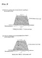
- Fig. 2 shows a diagram for schematically comparing and illustrating difference in the sectional shape of the circuit obtained by the present invention and the sectional shape of the circuit obtained by a conventional method.
- Fig. 3 shows diagrams showing the relationship between the dissolution rate and the hardness of copper.
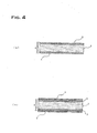
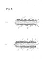
- Figs. 4 to 6 show schematic diagrams representing the manufacturing flow of a printed wiring board.
- the inventors of the present invention conducted intensive studies, and found that the above problems could be solved by designing a copper clad laminate considering the characteristics of a copper foil for laying on the copper clad laminate, and the copper-plated circuit layer formed thereon. That is, by paying attention to difference in dissolution rates to an etchant between the copper-plated circuit layer and the copper foil layer, a certain level or more of difference in dissolution rates was produced between the two, and by using a specific etchant, a high-quality printed wiring board that could not be obtained by prior art could be manufactured using a semi-additive method.
- a copper clad laminate comprising a copper-plated circuit layer for manufacturing a printed wiring board by a semi-additive method
- the copper clad laminate with a copper-plated circuit layer characterized by comprising a copper-plated circuit layer and an outer-layer copper foil layer that satisfied the relationship wherein, when a specific etchant is used, the Rv value (Vsc/Vsp), which is the ratio of the dissolution rate (Vsp) of deposited copper that constitutes said copper-plated circuit layer to the dissolution rate (Vsc) of copper that constitutes said outer-layer copper foil layer, is 1.0 or more.
- Fig. 1 shows a schematic cross section of the copper clad laminate with a copper-plated circuit layer.
- the copper clad laminate with a copper-plated circuit layer means the state when the processes to the step (2) of the above-described conventional semi-additive method have been completed.
- a copper clad laminate with a copper-plated circuit layer has the Rv value (Vsc/Vsp), which is the ratio of the dissolution rate (Vsp) of deposited copper that constitutes said copper-plated circuit layer to the dissolution rate (Vsc) of copper that constitutes said outer-layer copper foil layer, is 1.0 or more, then the erosion of the upper edge portion of the copper-plated circuit layer is prevented when the copper foil layer is removed by flush etching in the following step, and the deterioration of the circuit pattern of the printed wiring board, which is the end product, can be avoided.
- Vsc/Vsp the ratio of the dissolution rate (Vsp) of deposited copper that constitutes said copper-plated circuit layer to the dissolution rate (Vsc) of copper that constitutes said outer-layer copper foil layer
- Fig. 2 (b) shows, the edge portions on the upper portion of the cross section of the formed circuit is eroded, and the corners are rounded. As a result, the flat region on the upper portion of the circuit is narrowed.
- the use of the copper clad laminate with the copper-plated circuit layer prevents the erosion of the edge portions on the upper portion of the cross section of the formed circuit, and sharp corners as Fig. 2 (c) shows remain intact.
- the flat region on the upper portion of the circuit is widened, the initially designed circuit width can be achieved easily, and finishing accuracy becomes favorable.
- the connecting area for mounting the parts is widened, and process control if facilitated.
- the dissolution rate (Vsp) of the deposited copper constituting the copper-plated circuit layer is slower than the dissolution rate (Vsc) of the copper constituting the above-described outer-layer copper foil layer, the object cannot be achieved obviously. Furthermore, strictly speaking, the dissolution rate differs depending on the type of the etchant. Also, the type of the etchant determines whether difference between Vsp and Vsc is large or not.
- the Rv value (Vsc/vsp) must be the value of 1. 0 or more.
- the Rv value is less than 1.0, the erosion of the copper-plated circuit layer portion increases, and the aspect ratio of the cross section of the circuit begins changing steeply. Therefore, as a matter of course, the larger difference enables the erosion of the copper-plated circuit layer to be prevented in the flush etching of the above-described semi-additive method.
- the claim uses the expression of "when a specific etchant is used" is used. This etchant will be described in detail below in the description of the manufacturing method.
- a copper clad laminate with a copper-plated circuit layer characterized in comprising a copper-plated circuit layer and an outer-layer copper foil layer that satisfied the relationship wherein, when a specific etchant is used, the Rhv value (Hvc/Hvp), which is the ratio of the Vickers' hardness (Hvp) of deposited copper that constitutes said copper-plated circuit layer to the dissolution rate (Hvc) of copper that constitutes said outer-layer copper foil layer, is 1.0 or less.
- the present inventors found, as the result of substituting the range where the above-described Rv value (Vsc/Vsp) is 1.0 or more with the value of Wickers hardness, that it is enough if the relationship wherein the Rhv value (Hvc/Hvp), which is the ratio of the Vickers' hardness (Hvp) of deposited copper that constitutes the copper-plated circuit layer to the Vickers' hardness (Hvc) of copper that constitutes said outer- layer copper foil layer, is 1.0 or less is satisfied.
- the present inventors used various solutions as the etchants in studying the above-described dissolution rate of copper. Typically, they were copper-chloride-based, iron-chloride-based, sulfuric acid/hydrogen peroxide-based solutions, and the like. Since there were cases to use additives that can be considered as a common sense in combination, the expression of "...-base" was used.
- a method for manufacturing a printed wiring board characterized in that, as an etchant used in flush etching for etching off the outer-layer copper foil layer at areas on which surface the copper-plated circuit layer is not formed and is exposed, any of copper-chloride-based, iron-chloride-based, or sulfuric acid/hydrogen peroxide-based copper etchants is employed.
- a copper clad laminate with a copper-plated circuit layer was manufactured, and subjecting the copper clad laminate with a copper-plated circuit layer to the flush etching to manufacture a printed wiring board. Then, the cross-sectional shape of the formed circuit was observed.
- a double-sided printed wiring board was manufactured using a semi-additive method.
- the embodiment will be described below with reference to the manufacturing flow shown in Figs. 4 to 6 . Therefore, here, a double-sided copper clad laminate 4, wherein electrodeposited copper foils 3 each having a nominal thickness of 5 ⁇ m were laid on the both surfaces of FR-4 prepreg 2 shown in Fig. 4 (a) as the outer layers, was used.
- plating resist layers 5 were formed on the both surfaces of the electrodeposited copper foils 3 laid on the outer layers of the double-sided copper clad laminate 4.
- dry films positive type
- each having a thickness of 25 ⁇ m were compressed with heated rollers with the use of a dry-film laminator.
- photo-mask films corresponding to the circuit pattern to be formed were placed on the plating resist layers 5 formed on the surfaces of the outer-layer copper foils, and exposed to UV radiation.
- the UV dose at this time was about 40 mJ/cm 2 .
- a positive-type dry film which has an exposure resolution superior to that of a so-called negative-type dry film, the portions of the plating resist layers 5 exposed to UV radiation were dissolved during developing, and the portions of the plating resist layers 5 not exposed to UV radiation were left after developing.
- the copper clad laminate with a copper-plated circuit layer 7 having a cross section shown in the schematic sectional view of Fig. 6 (e) was flush-etched using a solution containing 40 m/1 of sulfuric acid and 32 m/1 of hydrogen peroxide of a liquid temperature of 30°C as the etchant. As a result, a double-sided printed wiring board 1 of a cross section shown in the schematic sectional view of Fig. 6 (f) was obtained.
- the circuit of a printed wiring board obtained with the use of a copper clad laminate with a copper-plated circuit layer according to the present invention through the manufacturing method according to the present invention can possess a cross-sectional shape having a very excellent aspect ratio, can easily obtain the circuit width as designed, and excels in finishing accuracy in the level that cannot be obtained by prior art. Moreover, it becomes possible to secure a large part mounting area for mounting parts, to reduce the costs for process control, and to contribute to the reduction of total manufacturing costs.
Landscapes
- Engineering & Computer Science (AREA)
- Manufacturing & Machinery (AREA)
- Microelectronics & Electronic Packaging (AREA)
- Manufacturing Of Printed Circuit Boards (AREA)
- Manufacturing Of Printed Wiring (AREA)
- Electroplating Methods And Accessories (AREA)
- ing And Chemical Polishing (AREA)
- Parts Printed On Printed Circuit Boards (AREA)
- Laminated Bodies (AREA)
Applications Claiming Priority (2)
| Application Number | Priority Date | Filing Date | Title |
|---|---|---|---|
| JP2001163743A JP4683769B2 (ja) | 2001-05-31 | 2001-05-31 | 銅メッキ回路層付銅張積層板及びその銅メッキ回路層付銅張積層板を用いたプリント配線板の製造方法 |
| EP02733250A EP1392092A4 (de) | 2001-05-31 | 2002-05-30 | Verkupferte schaltungsschicht-tragendes kupferbeschichtetes laminiertes blatt und verfahren zur herstellung einer leiterplattenverdrahtung damit |
Related Parent Applications (1)
| Application Number | Title | Priority Date | Filing Date |
|---|---|---|---|
| EP02733250.1 Division | 2002-05-30 |
Publications (2)
| Publication Number | Publication Date |
|---|---|
| EP2398304A2 true EP2398304A2 (de) | 2011-12-21 |
| EP2398304A3 EP2398304A3 (de) | 2012-10-10 |
Family
ID=19006653
Family Applications (2)
| Application Number | Title | Priority Date | Filing Date |
|---|---|---|---|
| EP11180970A Withdrawn EP2398304A3 (de) | 2001-05-31 | 2002-05-30 | Kupferkaschiertes Laminat mit kupferplattierter Leitungsschicht und Verfahren zur Herstellung einer Leiterplatte unter Verwendung des kupferkaschierten Laminats mit der kupferplattierten Leitungsschicht |
| EP02733250A Ceased EP1392092A4 (de) | 2001-05-31 | 2002-05-30 | Verkupferte schaltungsschicht-tragendes kupferbeschichtetes laminiertes blatt und verfahren zur herstellung einer leiterplattenverdrahtung damit |
Family Applications After (1)
| Application Number | Title | Priority Date | Filing Date |
|---|---|---|---|
| EP02733250A Ceased EP1392092A4 (de) | 2001-05-31 | 2002-05-30 | Verkupferte schaltungsschicht-tragendes kupferbeschichtetes laminiertes blatt und verfahren zur herstellung einer leiterplattenverdrahtung damit |
Country Status (7)
| Country | Link |
|---|---|
| US (1) | US6652993B2 (de) |
| EP (2) | EP2398304A3 (de) |
| JP (1) | JP4683769B2 (de) |
| KR (1) | KR100866440B1 (de) |
| CN (1) | CN1222203C (de) |
| TW (1) | TW550982B (de) |
| WO (1) | WO2002098194A1 (de) |
Families Citing this family (12)
| Publication number | Priority date | Publication date | Assignee | Title |
|---|---|---|---|---|
| JP2007081214A (ja) * | 2005-09-15 | 2007-03-29 | Mitsui Mining & Smelting Co Ltd | プリント配線基板の製造方法 |
| JP2007095910A (ja) * | 2005-09-28 | 2007-04-12 | Elna Co Ltd | 配線基板の製造方法 |
| KR100685177B1 (ko) * | 2006-03-10 | 2007-02-22 | 삼성전기주식회사 | 보드 온 칩 패키지 및 그 제조 방법 |
| JP2012501084A (ja) * | 2008-08-27 | 2012-01-12 | エーエムオー ゲーエムベーハー | 改良型ナノインプリント方法 |
| CN101977482B (zh) * | 2010-11-09 | 2012-03-28 | 深圳崇达多层线路板有限公司 | 一种高纵横比的pcb产品外层线路蚀刻方法 |
| EP2566311A1 (de) * | 2011-09-02 | 2013-03-06 | Atotech Deutschland GmbH | Direktplattierungsverfahren |
| EP2594662B1 (de) * | 2011-11-21 | 2014-04-09 | Atotech Deutschland GmbH | Wässrige Zusammensetzung zur Ätzung von Kupfer und Kupferlegierungen |
| CN105188271B (zh) * | 2012-01-17 | 2017-12-05 | 江苏普诺威电子股份有限公司 | 加成法凸台印制板制作工艺 |
| US20140123487A1 (en) * | 2012-11-08 | 2014-05-08 | Boardtek Electronics Corporation | Printed circuit board manufacturing method |
| JP2015134953A (ja) | 2014-01-17 | 2015-07-27 | Jx日鉱日石金属株式会社 | 表面処理銅箔、キャリア付銅箔、プリント配線板、プリント回路板、銅張積層板及びプリント配線板の製造方法 |
| CN109429434A (zh) * | 2017-08-31 | 2019-03-05 | 鹏鼎控股(深圳)股份有限公司 | 电路板及其制作方法 |
| CN114786365B (zh) * | 2022-04-14 | 2024-12-13 | 扬州华盟电子有限公司 | 一种无线充电用柔性线路板及其制作方法与应用 |
Family Cites Families (15)
| Publication number | Priority date | Publication date | Assignee | Title |
|---|---|---|---|---|
| US4383003A (en) * | 1980-09-22 | 1983-05-10 | General Electric Company | Transfer lamination of copper thin sheets and films, method and product |
| US4458052A (en) * | 1982-06-23 | 1984-07-03 | Mobil Oil Corporation | Alkyl sulfonates of polyvinyl alcohol as viscosifiers in saline solutions |
| US4806200A (en) * | 1986-06-18 | 1989-02-21 | Macdermid, Incorporated | Method for manufacture of printed circuit boards |
| US5049244A (en) * | 1989-01-20 | 1991-09-17 | Casio Computer Co., Ltd. | Method of manufacturing double-sided wiring substrate |
| GB2259812B (en) * | 1991-09-06 | 1996-04-24 | Toa Gosei Chem Ind | Method for making multilayer printed circuit board having blind holes and resin-coated copper foil used for the method |
| DE4231535C2 (de) * | 1991-09-20 | 1997-12-11 | Hitachi Ltd | Verfahren zur Erzeugung eines leitenden Schaltungsmusters |
| JPH05175640A (ja) * | 1991-12-26 | 1993-07-13 | Hitachi Ltd | プリント基板製造方法 |
| US5262041A (en) * | 1992-12-11 | 1993-11-16 | Shipley Company Inc. | Additive plating process |
| JPH07329246A (ja) * | 1994-06-08 | 1995-12-19 | Hitachi Chem Co Ltd | 金属張り積層板及びその製造法 |
| US5733468A (en) * | 1996-08-27 | 1998-03-31 | Conway, Jr.; John W. | Pattern plating method for fabricating printed circuit boards |
| JP3184485B2 (ja) * | 1997-11-06 | 2001-07-09 | 三井金属鉱業株式会社 | 銅張積層板用樹脂組成物、樹脂付き銅箔、多層銅張り積層板および多層プリント配線板 |
| JPH11302809A (ja) | 1998-04-16 | 1999-11-02 | Mitsui Chem Inc | 銅薄膜基板及びプリント配線板の製造法 |
| SG101924A1 (en) * | 1998-10-19 | 2004-02-27 | Mitsui Mining & Smelting Co | Composite material used in making printed wiring boards |
| US6212769B1 (en) * | 1999-06-29 | 2001-04-10 | International Business Machines Corporation | Process for manufacturing a printed wiring board |
| JP2001111201A (ja) * | 1999-10-14 | 2001-04-20 | Matsushita Electric Ind Co Ltd | 配線板の製造方法およびそれを用いて製造された配線板 |
-
2001
- 2001-05-31 JP JP2001163743A patent/JP4683769B2/ja not_active Expired - Lifetime
-
2002
- 2002-04-25 US US10/131,222 patent/US6652993B2/en not_active Expired - Lifetime
- 2002-04-30 TW TW091109036A patent/TW550982B/zh not_active IP Right Cessation
- 2002-05-30 EP EP11180970A patent/EP2398304A3/de not_active Withdrawn
- 2002-05-30 EP EP02733250A patent/EP1392092A4/de not_active Ceased
- 2002-05-30 CN CNB028023013A patent/CN1222203C/zh not_active Expired - Lifetime
- 2002-05-30 KR KR1020037001479A patent/KR100866440B1/ko not_active Expired - Lifetime
- 2002-05-30 WO PCT/JP2002/005255 patent/WO2002098194A1/ja not_active Ceased
Non-Patent Citations (1)
| Title |
|---|
| None |
Also Published As
| Publication number | Publication date |
|---|---|
| WO2002098194A1 (fr) | 2002-12-05 |
| EP1392092A4 (de) | 2007-05-02 |
| TW550982B (en) | 2003-09-01 |
| CN1465216A (zh) | 2003-12-31 |
| US6652993B2 (en) | 2003-11-25 |
| KR100866440B1 (ko) | 2008-10-31 |
| US20020182434A1 (en) | 2002-12-05 |
| EP1392092A1 (de) | 2004-02-25 |
| JP2002359454A (ja) | 2002-12-13 |
| EP2398304A3 (de) | 2012-10-10 |
| JP4683769B2 (ja) | 2011-05-18 |
| CN1222203C (zh) | 2005-10-05 |
| KR20030017662A (ko) | 2003-03-03 |
Similar Documents
| Publication | Publication Date | Title |
|---|---|---|
| US6652993B2 (en) | Cooper clad laminate with cooper-plated circuit layer, and method for manufacturing printed wiring board using the copper clad laminate with cooper-plated circuit layer | |
| CA2336918C (en) | Improved method for forming conductive traces and printed circuits made thereby | |
| DE112006003899T5 (de) | Verfahren zur Bildung eines Resistmusters, Verfahren zur Herstellung einer Leiterplatte sowie Leiterplatte | |
| JPH07273448A (ja) | プリント回路基板とフィルム回路基板およびそれらの製造方法、ならびにプリント回路基板とフィルム回路基板用中間物 | |
| KR20120007909A (ko) | 프린트기판의 제조방법 | |
| US5733468A (en) | Pattern plating method for fabricating printed circuit boards | |
| EP1335643A2 (de) | Verfahren zur Herstellung einer doppelseitigen Leiterplatte | |
| KR100899588B1 (ko) | 인쇄 회로 기판 제조에서 옥사이드 공정을 대체하고 미세라인을 제조하기 위해 구리 포일을 금속 처리하는 인쇄회로 기판 제조 방법 | |
| US8074352B2 (en) | Method of manufacturing printed circuit board | |
| CN105323953A (zh) | 印刷线路板及其制造方法 | |
| CN116033663B (zh) | 精细柔性线路板及其线路蚀刻补偿方法 | |
| CN118899229A (zh) | 无芯封装基板制作方法及无芯封装基板 | |
| US20030226687A1 (en) | Method of manufacturing printed wiring board and printed wiring board obtained by the manufacturing method | |
| JP2003031927A (ja) | プリント配線板の製造方法 | |
| EP0949855B1 (de) | Verfahren zur Herstellung einer mit elektroplattiertem Sackloch versehenen mehrschichtige Leiterplatte | |
| JPH0243356B2 (de) | ||
| JP4730222B2 (ja) | 配線基板の製造方法 | |
| JPH04286389A (ja) | 回路基板の製造方法 | |
| KR102767755B1 (ko) | 미세 상호 연결을 갖는 회로 기판을 제조하기 위한 차감 방법 | |
| CN120076205B (zh) | 一种通孔单面孔环的高精度电路板制作方法 | |
| JP2006173597A (ja) | レジストパターンの形成方法、回路基板の製造方法及び回路基板 | |
| JP4628993B2 (ja) | 回路基板の製造方法 | |
| JP3187630B2 (ja) | 電鋳法 | |
| JP2002314228A (ja) | 配線回路基板およびその製造方法 | |
| JPH03124090A (ja) | プリント配線板のパターンめっき形成方法 |
Legal Events
| Date | Code | Title | Description |
|---|---|---|---|
| AC | Divisional application: reference to earlier application |
Ref document number: 1392092 Country of ref document: EP Kind code of ref document: P |
|
| AK | Designated contracting states |
Kind code of ref document: A2 Designated state(s): DE FR GB LU |
|
| PUAI | Public reference made under article 153(3) epc to a published international application that has entered the european phase |
Free format text: ORIGINAL CODE: 0009012 |
|
| PUAL | Search report despatched |
Free format text: ORIGINAL CODE: 0009013 |
|
| AK | Designated contracting states |
Kind code of ref document: A3 Designated state(s): DE FR GB LU |
|
| RIC1 | Information provided on ipc code assigned before grant |
Ipc: H05K 3/10 20060101AFI20120831BHEP Ipc: C23F 1/18 20060101ALI20120831BHEP Ipc: C25D 7/00 20060101ALI20120831BHEP Ipc: C23F 1/00 20060101ALI20120831BHEP Ipc: C25D 5/48 20060101ALI20120831BHEP |
|
| STAA | Information on the status of an ep patent application or granted ep patent |
Free format text: STATUS: THE APPLICATION IS DEEMED TO BE WITHDRAWN |
|
| 18D | Application deemed to be withdrawn |
Effective date: 20130411 |