EP2390699B1 - Optisches Kupplungsmodul mit optischer Wellenleiterstruktur - Google Patents
Optisches Kupplungsmodul mit optischer Wellenleiterstruktur Download PDFInfo
- Publication number
- EP2390699B1 EP2390699B1 EP11167325.7A EP11167325A EP2390699B1 EP 2390699 B1 EP2390699 B1 EP 2390699B1 EP 11167325 A EP11167325 A EP 11167325A EP 2390699 B1 EP2390699 B1 EP 2390699B1
- Authority
- EP
- European Patent Office
- Prior art keywords
- optical
- film
- signal
- coupler module
- optical coupler
- Prior art date
- Legal status (The legal status is an assumption and is not a legal conclusion. Google has not performed a legal analysis and makes no representation as to the accuracy of the status listed.)
- Not-in-force
Links
- 230000003287 optical effect Effects 0.000 title claims description 286
- 230000005540 biological transmission Effects 0.000 claims description 78
- 239000004065 semiconductor Substances 0.000 claims description 46
- 239000000758 substrate Substances 0.000 claims description 43
- 239000013307 optical fiber Substances 0.000 claims description 33
- 238000006243 chemical reaction Methods 0.000 claims description 24
- 239000010410 layer Substances 0.000 claims description 9
- 238000005516 engineering process Methods 0.000 claims description 5
- 239000007769 metal material Substances 0.000 claims description 5
- 230000004044 response Effects 0.000 claims description 5
- 229910052710 silicon Inorganic materials 0.000 claims description 5
- 239000010703 silicon Substances 0.000 claims description 5
- 239000000463 material Substances 0.000 claims description 3
- 230000003667 anti-reflective effect Effects 0.000 claims description 2
- 239000012212 insulator Substances 0.000 claims description 2
- 230000010287 polarization Effects 0.000 claims description 2
- 239000002356 single layer Substances 0.000 claims description 2
- 238000000034 method Methods 0.000 description 10
- 238000010586 diagram Methods 0.000 description 9
- 230000008569 process Effects 0.000 description 9
- 238000013461 design Methods 0.000 description 7
- 238000012986 modification Methods 0.000 description 5
- 230000004048 modification Effects 0.000 description 5
- 230000008878 coupling Effects 0.000 description 4
- 238000010168 coupling process Methods 0.000 description 4
- 238000005859 coupling reaction Methods 0.000 description 4
- XUIMIQQOPSSXEZ-UHFFFAOYSA-N Silicon Chemical compound [Si] XUIMIQQOPSSXEZ-UHFFFAOYSA-N 0.000 description 3
- 230000000694 effects Effects 0.000 description 3
- RYGMFSIKBFXOCR-UHFFFAOYSA-N Copper Chemical compound [Cu] RYGMFSIKBFXOCR-UHFFFAOYSA-N 0.000 description 2
- 239000011248 coating agent Substances 0.000 description 2
- 238000000576 coating method Methods 0.000 description 2
- 229910052802 copper Inorganic materials 0.000 description 2
- 239000010949 copper Substances 0.000 description 2
- 239000002861 polymer material Substances 0.000 description 2
- 230000005855 radiation Effects 0.000 description 2
- 230000008054 signal transmission Effects 0.000 description 2
- VYPSYNLAJGMNEJ-UHFFFAOYSA-N Silicium dioxide Chemical compound O=[Si]=O VYPSYNLAJGMNEJ-UHFFFAOYSA-N 0.000 description 1
- 230000009471 action Effects 0.000 description 1
- 230000000712 assembly Effects 0.000 description 1
- 238000000429 assembly Methods 0.000 description 1
- 238000011161 development Methods 0.000 description 1
- 238000005530 etching Methods 0.000 description 1
- 230000017525 heat dissipation Effects 0.000 description 1
- 230000010354 integration Effects 0.000 description 1
- 229910021421 monocrystalline silicon Inorganic materials 0.000 description 1
- 238000012545 processing Methods 0.000 description 1
- 229910052814 silicon oxide Inorganic materials 0.000 description 1
- 239000002210 silicon-based material Substances 0.000 description 1
Images


Classifications
-
- G—PHYSICS
- G02—OPTICS
- G02B—OPTICAL ELEMENTS, SYSTEMS OR APPARATUS
- G02B6/00—Light guides; Structural details of arrangements comprising light guides and other optical elements, e.g. couplings
- G02B6/24—Coupling light guides
- G02B6/42—Coupling light guides with opto-electronic elements
-
- G—PHYSICS
- G02—OPTICS
- G02B—OPTICAL ELEMENTS, SYSTEMS OR APPARATUS
- G02B6/00—Light guides; Structural details of arrangements comprising light guides and other optical elements, e.g. couplings
- G02B6/24—Coupling light guides
- G02B6/42—Coupling light guides with opto-electronic elements
- G02B6/4201—Packages, e.g. shape, construction, internal or external details
- G02B6/4204—Packages, e.g. shape, construction, internal or external details the coupling comprising intermediate optical elements, e.g. lenses, holograms
- G02B6/4214—Packages, e.g. shape, construction, internal or external details the coupling comprising intermediate optical elements, e.g. lenses, holograms the intermediate optical element having redirecting reflective means, e.g. mirrors, prisms for deflecting the radiation from horizontal to down- or upward direction toward a device
-
- G—PHYSICS
- G02—OPTICS
- G02B—OPTICAL ELEMENTS, SYSTEMS OR APPARATUS
- G02B6/00—Light guides; Structural details of arrangements comprising light guides and other optical elements, e.g. couplings
- G02B6/24—Coupling light guides
- G02B6/42—Coupling light guides with opto-electronic elements
- G02B6/4201—Packages, e.g. shape, construction, internal or external details
- G02B6/4249—Packages, e.g. shape, construction, internal or external details comprising arrays of active devices and fibres
-
- G—PHYSICS
- G02—OPTICS
- G02B—OPTICAL ELEMENTS, SYSTEMS OR APPARATUS
- G02B6/00—Light guides; Structural details of arrangements comprising light guides and other optical elements, e.g. couplings
- G02B6/24—Coupling light guides
- G02B6/42—Coupling light guides with opto-electronic elements
- G02B6/43—Arrangements comprising a plurality of opto-electronic elements and associated optical interconnections
-
- H—ELECTRICITY
- H01—ELECTRIC ELEMENTS
- H01L—SEMICONDUCTOR DEVICES NOT COVERED BY CLASS H10
- H01L2224/00—Indexing scheme for arrangements for connecting or disconnecting semiconductor or solid-state bodies and methods related thereto as covered by H01L24/00
- H01L2224/01—Means for bonding being attached to, or being formed on, the surface to be connected, e.g. chip-to-package, die-attach, "first-level" interconnects; Manufacturing methods related thereto
- H01L2224/10—Bump connectors; Manufacturing methods related thereto
- H01L2224/15—Structure, shape, material or disposition of the bump connectors after the connecting process
- H01L2224/16—Structure, shape, material or disposition of the bump connectors after the connecting process of an individual bump connector
- H01L2224/161—Disposition
- H01L2224/16151—Disposition the bump connector connecting between a semiconductor or solid-state body and an item not being a semiconductor or solid-state body, e.g. chip-to-substrate, chip-to-passive
- H01L2224/16221—Disposition the bump connector connecting between a semiconductor or solid-state body and an item not being a semiconductor or solid-state body, e.g. chip-to-substrate, chip-to-passive the body and the item being stacked
- H01L2224/16225—Disposition the bump connector connecting between a semiconductor or solid-state body and an item not being a semiconductor or solid-state body, e.g. chip-to-substrate, chip-to-passive the body and the item being stacked the item being non-metallic, e.g. insulating substrate with or without metallisation
-
- H—ELECTRICITY
- H01—ELECTRIC ELEMENTS
- H01L—SEMICONDUCTOR DEVICES NOT COVERED BY CLASS H10
- H01L2224/00—Indexing scheme for arrangements for connecting or disconnecting semiconductor or solid-state bodies and methods related thereto as covered by H01L24/00
- H01L2224/01—Means for bonding being attached to, or being formed on, the surface to be connected, e.g. chip-to-package, die-attach, "first-level" interconnects; Manufacturing methods related thereto
- H01L2224/42—Wire connectors; Manufacturing methods related thereto
- H01L2224/44—Structure, shape, material or disposition of the wire connectors prior to the connecting process
- H01L2224/45—Structure, shape, material or disposition of the wire connectors prior to the connecting process of an individual wire connector
- H01L2224/45001—Core members of the connector
- H01L2224/45099—Material
- H01L2224/451—Material with a principal constituent of the material being a metal or a metalloid, e.g. boron (B), silicon (Si), germanium (Ge), arsenic (As), antimony (Sb), tellurium (Te) and polonium (Po), and alloys thereof
- H01L2224/45138—Material with a principal constituent of the material being a metal or a metalloid, e.g. boron (B), silicon (Si), germanium (Ge), arsenic (As), antimony (Sb), tellurium (Te) and polonium (Po), and alloys thereof the principal constituent melting at a temperature of greater than or equal to 950°C and less than 1550°C
- H01L2224/45147—Copper (Cu) as principal constituent
-
- H—ELECTRICITY
- H01—ELECTRIC ELEMENTS
- H01L—SEMICONDUCTOR DEVICES NOT COVERED BY CLASS H10
- H01L2224/00—Indexing scheme for arrangements for connecting or disconnecting semiconductor or solid-state bodies and methods related thereto as covered by H01L24/00
- H01L2224/01—Means for bonding being attached to, or being formed on, the surface to be connected, e.g. chip-to-package, die-attach, "first-level" interconnects; Manufacturing methods related thereto
- H01L2224/42—Wire connectors; Manufacturing methods related thereto
- H01L2224/47—Structure, shape, material or disposition of the wire connectors after the connecting process
- H01L2224/48—Structure, shape, material or disposition of the wire connectors after the connecting process of an individual wire connector
- H01L2224/4805—Shape
- H01L2224/4809—Loop shape
- H01L2224/48091—Arched
-
- H—ELECTRICITY
- H01—ELECTRIC ELEMENTS
- H01L—SEMICONDUCTOR DEVICES NOT COVERED BY CLASS H10
- H01L2924/00—Indexing scheme for arrangements or methods for connecting or disconnecting semiconductor or solid-state bodies as covered by H01L24/00
- H01L2924/15—Details of package parts other than the semiconductor or other solid state devices to be connected
- H01L2924/151—Die mounting substrate
- H01L2924/1517—Multilayer substrate
- H01L2924/15172—Fan-out arrangement of the internal vias
- H01L2924/15174—Fan-out arrangement of the internal vias in different layers of the multilayer substrate
-
- H—ELECTRICITY
- H01—ELECTRIC ELEMENTS
- H01L—SEMICONDUCTOR DEVICES NOT COVERED BY CLASS H10
- H01L2924/00—Indexing scheme for arrangements or methods for connecting or disconnecting semiconductor or solid-state bodies as covered by H01L24/00
- H01L2924/15—Details of package parts other than the semiconductor or other solid state devices to be connected
- H01L2924/151—Die mounting substrate
- H01L2924/1517—Multilayer substrate
- H01L2924/15192—Resurf arrangement of the internal vias
-
- H—ELECTRICITY
- H01—ELECTRIC ELEMENTS
- H01L—SEMICONDUCTOR DEVICES NOT COVERED BY CLASS H10
- H01L2924/00—Indexing scheme for arrangements or methods for connecting or disconnecting semiconductor or solid-state bodies as covered by H01L24/00
- H01L2924/15—Details of package parts other than the semiconductor or other solid state devices to be connected
- H01L2924/151—Die mounting substrate
- H01L2924/153—Connection portion
- H01L2924/1531—Connection portion the connection portion being formed only on the surface of the substrate opposite to the die mounting surface
- H01L2924/15311—Connection portion the connection portion being formed only on the surface of the substrate opposite to the die mounting surface being a ball array, e.g. BGA
Definitions
- the present invention relates to an optical coupler module having an optical waveguide structure, and more particularly to a receiver module, a transmitter module or a transceiver module having the optical waveguide structure for converting and transmitting optical/electrical signals with total internal reflection phenomenon.
- copper wires are widely used for transmitting electrical signals or data between different components in a cheap and convenient way.
- a high performance electronic system since more and more processors are provided and the signal processing speed upgrades, it is important to enhance the quality and speed of transmitting the signals and data between the processors.
- the conventional copper wires fail to meet these requirements.
- An optical coupler device may be used to convert electrical signals into optical signals, convert optical signals into electrical signals, and emit and receive the electrical signals and optical signals.
- the optical coupler device includes for example an optical emitter or a light source unit for emitting optical signals, an optical receiver or a light-detecting unit for receiving optical signals, or a driver circuit or an amplifier circuit for driving these units or amplifying these signals.
- the optical emitter and the optical receiver are usually packaged in a coupler module and there is no electrical or physical connection therein. In other words, the electrical interference is eliminated as much as possible for the optical coupler device.
- FIG. 1A a cross-sectional view illustrating the optical coupler device 101.
- the optical coupler device 101 1 includes a trench 105 defined in a semiconductor substrate 103.
- a reflector 107 is defined at a first end of the trench 105, and there is an angle between the reflector 107 and the lengthwise direction of the trench 105.
- An optical fiber 109 is disposed in the trench 105 at a second end of the trench 105.
- An optical device 111 is mounted on the semiconductor substrate 103 proximate to the trench 105 such that the optical device 111 is optically coupled to the optical fiber 109 via the reflector 107.
- the optical device 111 may be an optical emitter for outputting optical signals 113 or an optical receiver for receiving optical signals 113.
- the semiconductor substrate 103 is mounted on a printed circuit board (PCB) 115 including contacts 117 which are electrically coupled to the semiconductor substrate 103.
- a circuit 125 is included in another semiconductor substrate 127 which is mounted on the semiconductor substrate 103 by contacts 131.
- the circuit 125 can drive or control the optical device 111 to convert electrical signals 119 from the contacts 117 into optical signals 113.
- the optical signals 113 are reflected by the reflector 107 and outputted through the optical fiber 109. In a reverse direction, the optical signals 113 inputted from the optical fiber 109 are reflected by the reflector 107 and received by the optical device 111.
- the optical signals 113 are converted into electrical signals 119 to be outputted through the contacts 117.
- a lid 133 is mounted over the semiconductor substrate 103 and encloses the optical device 111. The lid 133 protects the enclosed items.
- a plurality of corresponding optical devices 111, trenches 105 and optical fibers 109 may be included in an optical coupler device 101. As shown in FIG. 1B , two optical coupler devices 101a and 101b, each including a plurality of corresponding optical devices 111, trenches 105 and optical fibers 109, are connected to each other through the representative optical fibers 109a and 109b to achieve signal transmission.
- an optical coupler module converts and transmits an electrical signal or an optical signal, and includes a semiconductor substrate, a first film, a second film, an electrical transmission unit, at least one signal conversion unit and an optical waveguide structure.
- the first film and the second film are formed on opposite surfaces of the semiconductor substrate.
- the electrical transmission unit is mounted on the first film and responsible for transmitting electrical signals.
- the signal conversion unit is mounted on and electrically connected to the electrical transmission unit for converting the electrical signal or the optical signal.
- the optical waveguide structure formed on the second film has a reflector and a waveguide body. The optical signal generated from the signal conversion unit sequentially passes the first film, the semiconductor substrate and the second film and enters the optical waveguide structure. Then, the optical signal is reflected by the reflector and transmitted in the waveguide body to be outputted. Alternatively, the optical signal is transmitted in a reverse direction from the optical waveguide structure to the signal conversion unit.
- the optical coupler module converts and transmits an electrical signal or an optical signal, and includes a semiconductor substrate, a first film, a second film, a control circuit, at least one signal conversion unit and at least one optical waveguide structure.
- the first film and the second film are formed on opposite surfaces of the semiconductor substrate.
- the control circuit with operation function is mounted on the first film and adjacent to the first film.
- the signal conversion unit is mounted above the first film and electrically connected to the control circuit for converting the electrical signal or the optical signal.
- the optical waveguide structure formed on the second film has a reflector and a waveguide body.
- the optical signal generated from the signal conversion unit sequentially passes the first film, the semiconductor substrate and the second film and enters the optical waveguide structure. Then, the optical signal is reflected by the reflector and transmitted in the waveguide body to be outputted. Alternatively, the optical signal is transmitted in a reverse direction from the optical waveguide structure to the signal conversion unit.
- FIG. 1A is a cross-sectional view illustrating a conventional optical coupler device
- FIG. 2A is a cross-sectional view illustrating an embodiment of a transmitter module according to the present invention.
- FIG. 2B is schematic diagram showing light path of the optical signals in the transmitter module of FIG. 2A ;
- FIG. 3A is a cross-sectional view illustrating the profile of the optical waveguide structure in FIG. 2A ;
- FIG. 3B is a perspective view showing the bottom of the transmitter module of FIG. 2A ;
- FIG. 4 is a perspective view illustrating the transmitter module according to the present invention.
- FIG. 5 is a cross-sectional view illustrating an embodiment of a receiver module according to the present invention.
- FIG. 6 is a schematic diagram showing the optical connection between the transmitter module and the receiver module according to the present invention.
- FIGs. 7A ⁇ 7D are schematic diagrams showing different modified embodiments of the transmitter modules according to the present invention.
- FIG. 8A is a cross-sectional view illustrating another modified embodiment of the transmitter module of FIG. 2A according to the present invention.
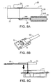
- FIG. 8B is a perspective diagram illustrating a connector for the optical coupler module of the present invention.
- FIG. 8C is a schematic diagram showing the coupling of the connector of FIG. 8B to a transmission interface according to the present invention.
- FIG. 9 is a schematic diagram showing the coupling of an optical fiber to the transmitter module according to the present invention.
- FIG. 10A is a schematic diagram showing the optical connection between a transmitter module and a receiver module according to the present invention.
- FIG. 10B is a schematic diagram showing the optical connection between a transmitter module and a chip according to the present invention.
- the structure of the conventional optical coupler device e.g. transmitter module and receiver module is too complicated to be easily and precisely manufactured.
- the optical transmission between the optical coupler device and the optical fiber is possibly affected due to a slight assembly error.
- an optical coupler module e.g. a transmitter module for electrical-optical signal conversion, a receiver module for optical-electrical signal conversion or a transceiver module for both conversions.
- the optical coupler module is manufactured by easier semiconductor process and can be assembled under certain tolerance, but with excellent quality of signal conversion and transmission.
- FIG. 2A a cross-sectional view illustrating an embodiment of a transmitter module according to the present invention.
- the transmitter module 2 includes a semiconductor substrate 20, a light source unit 24 and an optical waveguide structure 26.
- the semiconductor substrate 20 supports the light source unit 24 on its surface.
- the semiconductor substrate 20 is a monocrystalline silicon substrate in a form of double-sided polished silicon-on-insulator (SOI) wafer, but is not limited to this.
- SOI silicon-on-insulator
- a first film 21 and a second film 22 are formed on two opposite surfaces 201 and 202 of the semiconductor substrate 20, respectively.
- the first film 21 provides electrical-insulating effect and confines electrical/optical signals to avoid electrical interference in optical transmission. Since the optical signals travel through the first film 21 and the second film 22, the films 21 and 22 should be penetrable to optical signals as the semiconductor substrate 20.
- each of the films 21 and 22 is a single layer film made of silicon oxide, which is easily formed on the surface 201 or 202 of the semiconductor substrate 20 by known technology to assist the transmission of the optical signals.
- each of the films 21 and 22 is a multi-layer film with anti-reflecting coating.
- the second film 22 may provide electrical-insulating effect and confine electrical/optical signals.
- the films 21 and 22 can increase the tolerance of wavelength, angle of incidence and low polarization dependence.
- the light source unit 24 may include a light-emitting diode (LED), a semiconductor laser or a vertical cavity surface emitting laser (VCSEL) capable of emitting light beams or optical signals in response to electrical signals.
- the transmitter module 2 further includes an electrical transmission unit 23 on the first film 21.
- the light source unit 24 is mounted on and electrically connected to the electrical transmission unit 23.
- the transmitter module 2 may be mounted on or electrically connected to a printed circuit board to allow the transmitter module 2 to receive electrical signals 27 to be transmitted from the printed circuit board.
- the transmitter module 2 further includes a driving circuit 25 mounted on the first film 21 and electrically connected to the electrical transmission unit 23.
- the driving circuit 25 drives the light source unit 24 through the electrical transmission unit 23 to generate optical signals 28 in response to the electrical signals 27.
- the light source unit 24 is mounted on the electrical transmission unit 23 wherein a portion of the bottom area of the light source unit 24 touches the electrical transmission unit 23 to achieve the electrical connection.
- the transmitter module 2 may be implemented by system on chip (SoC) technology so that operation function is also integrated into the chip.
- SoC system on chip
- the integrated circuit (IC) with operation function is integrated into the driving circuit 25. Therefore, the driving circuit 25 may not only drive the light source unit 24 but also perform operation functionality.
- the electrical transmission unit 23 is made of metallic material for transmitting the electrical signals 27. Furthermore, the metallic material is advantageous to dissipate heat generated from the light source unit 24 during the conversion from the electrical signals 27 into the optical signals 28.
- the electrical transmission unit 23 made of metallic material and interfaced between the light source unit 24 and the first film 21 may effectively dissipate the heat by conduction or radiation.
- a via hole 230 is formed on the electrical transmission unit 23 so that the electrical transmission unit 23 does not obstruct the light path of the optical signals 28. Therefore, the optical signals 28 can pass the via hole of the electrical transmission unit 23, the first film 21 and the semiconductor substrate 20 for optical transmission.
- a via hole 230 is provided on the electrical transmission unit 23, the small size of the via hole 230 does not affect the heat-dissipation effect of the electrical transmission unit 23.
- the optical waveguide structure 26 is made of the same silicon material as the semiconductor substrate 20.
- the optical waveguide structure 26 is formed on the second film 22 and the position of the optical waveguide structure 26 corresponds to the position of the light source unit 23 so that the optical signals 28 provided by the light source unit 24 can enter the optical waveguide structure 26.
- the optical waveguide structure 26 includes a reflector 263 and a waveguide body 260.
- the optical signals 28 are reflected by the reflector 263 and the reflected optical signals 28 are transmitted along an axial or lengthwise direction of the waveguide body 260.
- the reflector 263 is arranged at a first end of the optical waveguide structure 26 and corresponds to the light source unit 24 so that the optical signals 28 can reach the reflector 263.
- the semiconductor substrate 20, the first film 21, the second film 22 and the optical waveguide structure 26 are formed in a semiconductor process. Particularly, after the second film 22 is formed on the second surface 202 of the semiconductor substrate 20, another silicon layer is formed on the second film 22. The silicon layer is partially etched to form a 45° slant surface at the first end 261. Suitable reflective coating is applied to the slant surface to form the reflector 263. Then, the light source unit 24, the electrical transmission unit 23 and the driving circuit 25 are mounted on the first film 21 by wafer bonding.
- the first film 21 and the second film 22 are dielectric films and penetrable to optical signals.
- the light source unit 24 emits the optical signals 28 in a "vertical" direction nearly normal to the second film 22 or the lengthwise direction of the optical waveguide structure 26.
- the optical signals 28 passes the first film 21, the semiconductor substrate 20 and the second film 22 to enter the first end 261 of the optical waveguide structure 26. Then, the optical signals 28 are reflected by the 45° reflector 263, transmitted by the waveguide body 260, and outputted from a second end 262 of the optical waveguide structure 26.
- FIG. 2B shows the light path of the optical signals 28 in the transmitter module 2. If the optical signals 28 enter the optical waveguide structure 26 at the first end 261 with an angle of incidence of 45°, the optical signals 28 are reflected and the reflected light direction is perpendicular to the incident direction. Therefore, the light path is parallel with the lengthwise direction of the waveguide body 260 and little energy loss occurs during the transmission.
- the light source unit 24 does not always emit "perfect" vertical light, that is, little scatter cannot be avoided.
- optical signals 28a and 28b enter the optical waveguide structure 26 at the first end 261 with little deviation from the perfect optical signals 28.
- the light paths of the reflected optical signals 28a and 28b are not parallel with the lengthwise direction of the waveguide body 260, and the reflected optical signals 28a and 28b will reach the surface of the waveguide body 260.
- the angle of incidence is greater than the critical angel for the interface between the waveguide body 260 and the second film 22 or the surrounding air. Therefore, total internal reflection occurs and the optical signals 28a and 28b do not escape from the waveguide body 260.
- the index of refraction of the second film 22 and the optical waveguide structure 26 should be taken into consideration to ensure total internal reflection.
- the index of refraction of the second film 22 should be smaller than that of the optical waveguide structure 26.
- FIG. 3A showing a profile of the second end 262 of the optical waveguide structure 26.
- the optical waveguide structure 26 has two symmetrical lateral surfaces, but is not limited to this.
- FIG. 3B showing the bottom of the transmitter module 2.
- the optical signals 28 are transmitted to the reflector 263, and total internal reflection occurs on the top surface and the bottom surface of the waveguide body 260. Therefore, the profile of the optical waveguide structure 26 has no particular restriction. Any profile with 45° slant surface for the reflector 263 and is easily obtained by an etching step is practicable.
- the transmitter module 2 may include more than one light source unit and corresponding optical waveguide structure to perform the optical transmission.
- the positions of the reflectors of the optical waveguide structures 26, 26a and 26b correspond to three light source units, respectively, so that the reflector of each of the optical waveguide structures 26, 26a and 26b may receive an optical signal from a corresponding light source unit.
- the transmitter module 2 includes four light source units 24, 24a, 24b and 24c for emitting optical signals.
- the four optical waveguide structures 26, 26a, 26b and 26c provided on the second film 22 receive optical signals from the corresponding light source units 24, 24a, 24b and 24c.
- the electrical transmission unit 23 includes four transmission lines connected to the driving circuit 25. Therefore, the driving circuit 25 drives the four light source units 24, 24a, 24b and 24c through the four transmission lines to generate four optical signals in response to four electrical signals to be transmitted by the four optical waveguide structures 26, 26a, 26b and 26c.
- a receiver module may be provided to receive optical signals, convert the optical signals into electrical signals, and output the electrical signals.
- FIG. 5 a cross-sectional view illustrating an embodiment of a receiver module according to the present invention.
- the receiver module 3 includes a semiconductor substrate 30, a light-detecting unit 34, an optical waveguide structure 36, an electrical transmission unit 33, an amplifier circuit 35, and two films 31 and 32 on opposite surfaces 301 and 302.
- the light source unit 24 and the driving circuit 25 of the transmitter module 2 are replaced by the light-detecting unit 34 and the amplifier circuit 35 in the receiver module 3.
- the detailed structure, material and function of the other components of the receiver module 3 are similar to those of the transmitter module 2 except the signal transmission direction and the conversion from the optical signal 38 into the electrical signal 37.
- the light-detecting unit 34 may include a photodiode or a photodetector capable of receiving and converting the optical signals 38 into electrical signals 37 for further transmission.
- the amplifier circuit 35 is usually implemented by a transimpedance amplifier.
- the optical waveguide structure 36 receives the external optical signals 38 at the second end 362, and the optical signals 38 are transmitted along the lengthwise direction of the waveguide body 360 with or without total internal reflection.
- the reflector 363 with a 45° slant surface at the first end 361 reflects the optical signals 38 to allow the optical signals 38 to pass through the second film 32, the semiconductor substrate 30, the first film 31 and the via hole 330 to reach the light-detecting unit 34.
- the optical signals 38 are converted into the electrical signals 37 by the light-detecting unit 34.
- the receiver module 3 may be mounted on and electrically connected to a printed circuit board.
- the amplifier circuit 35 amplifies and outputs the electrical signals 37 to the printed circuit board.
- the electrical transmission unit 33 made of metallic material and interfaced between the light-detecting unit 34 and the first film 31 may effectively dissipate the heat generated by the light-detecting unit 34 by conduction or radiation.
- the receiver module 3 may be implemented by a system on chip (SoC) technology so that operation function is also integrated into the chip.
- SoC system on chip
- the IC with operation function is integrated into the amplifier circuit 35. Therefore, the amplifier circuit 35 may not only amplify the electrical signals 37 but also perform operation functionality.
- the receiver module 3 may include a plurality of light-detecting unit 34 and corresponding optical waveguide structures 36 as above described with reference to FIG. 4 to perform multiple optical-electrical conversion and transmission.
- the optical coupler module according to the present invention has been described in the form of the transmitter module 2 and the receiver module 3.
- the optical coupler module may be a transceiver module by integrating the transmitter module 2 of FIG. 2A and the receiver module 3 of FIG. 5 capable of transmitting and receiving optical signals.
- the optical coupler module of FIG. 4 may include at least one light source unit and at least one light-detecting unit. Each one of the light source unit and the light-detecting unit is optically coupled to a corresponding optical waveguide structure.
- the optical coupler module e.g. the transmitter module, the receiving module or the transceiver module should be coupled to an optical transmission element such as an optical fiber so that the optical coupler module may receive optical signals from the optical transmission element or transmits optical signals to the optical transmission element.
- an optical transmission element such as an optical fiber
- the optical coupler module may receive optical signals from the optical transmission element or transmits optical signals to the optical transmission element.
- FIG. 6 showing the connection between the transmitter module and the receiver module according to the present invention.
- the transmitter module 2 and the receiver module 3 are respectively mounted on and electrically connected to the printed circuit boards 40 and 50.
- the printed circuit board 40 provides electrical signals to the transmitter module 2, and the printed circuit board 50 receives electrical signals from the receiver module 3.
- pin guides 41, 42, 51 and 52 provided on the printed circuit boards 40 and 50 for assembly of the printed circuit boards 40 and 50 and the optical fibers 60.
- pins 611, 612, 621 and 622 provided on two connectors 61 and 62 at two ends of the optical fibers 60.
- one of the transmitter module 2 and the receiver module 3 is coupled to one end of the optical fibers 60 through the connector 61 or 62 according to the present invention, while a conventional receiver module or transmitter module, e.g. optical coupler device with trenches as described in the prior arts, may be coupled to the other end of the optical fibers 60 through a conventional connector.
- a conventional receiver module or transmitter module e.g. optical coupler device with trenches as described in the prior arts
- the transmitter module and the receiver module concerning the position or the arrangement of the control circuit such as the driving circuit or the amplifier circuit.
- FIG. 7A showing another embodiment of the transmitter module 2a.
- the first film 21a does not cover all the first surface 201 of the semiconductor substrate 20. Only a portion of the first surface 201 where the light path of the optical signals 28 passes is covered by the first film 21a.
- the first film 21a is penetrable to optical signals 28 and anti-reflective.
- the driving circuit 25a is mounted on the other portion of the first surface 201 and adjacent to the first film 21a. According to the design, the electrical transmission unit is integrated into the driving circuit 25a, for example, the portion of the driving circuit 25a under the light source unit 24. Therefore, the driving circuit 25a forms a circuit layer on the first surface 201.
- the circuit layer is made by less line-width process, while the photonic layer is made by greater line-width process.
- the circuit layer and the photonic layer formed with different line-width processes are integrated on the silicon substrate 20 to form a monolithic optical-electrical/electrical-optical element.
- FIG. 7B illustrating another embodiment of the transmitter module 2b.
- the electrical transmission unit 23b is extended to cover the first surface 201 under the driving circuit 25b.
- the driving circuit 25b is mounted on the electrical transmission unit 23b by flip-chip process based on hybrid integration technique and electrically connected to the electrical transmission unit 23b.
- the top surface of the driving circuit 25b is aligned with the top surface of the light source unit 24.
- a third film 264 is formed on the second end of the optical waveguide structure 26.
- the material of the third film 264 may be the same as the first film 21 and the second film 22.
- the third film 264 can be applied to all the above-described embodiments.
- the driving circuit 25c is located on the printed circuit board 40 rather than on the electrical transmission unit 23c.
- an interconnect structure may be formed in the semiconductor substrate 20 to communicate the driving circuit 25c and the electrical transmission unit 23c, as shown in FIG. 7C .
- the driving circuit 25c may be electrically connected to the electrical transmission unit 23c by a wire, as shown in FIG. 7D . It is to be noted that the modifications, as described with reference to FIGs. 7A-7D , to the transmitter module 2 can be applied to the receiver module 3 or the transceiver module.
- the semiconductor substrate 20 and 30 separates the signal conversion unit, e.g. light source unit 24 and the light-detecting unit 34 from the optical waveguide structures 26 and 36, the optical signals 28 and 38 transmitted in the optical waveguide structures 26 and 36 are not affected by electrical interference. Furthermore, coupling the optical fibers to the optical waveguide structures 26 and 36 will not damage the sophisticated light source unit 24 and light-detecting unit 34.
- various modifications can be made to the assembly of the optical transmission system.
- FIG. 8A illustrating another embodiment of a transmitter module according to the present invention.
- a trench 203 is provided in the semiconductor substrate 20 near the second end of the optical waveguide structure 26 for accommodating the optical fiber 63.
- the profile of the trench 203 depends on the cross-section of the optical fiber 63, for example, U-shape or V-shape.
- the optical fiber 63 is put in the trench 203, the optical fiber 63 is coupled to the optical waveguide structure 26.
- the optical fiber 63 is fixed to the transmitter module 2 and cannot be removed.
- a pluggable design is applicable without affecting or damaging the light source unit 24 since the light source unit 24 is located at the other surface of the semiconductor substrate 20.
- the same design can be applied to other type of optical coupler module such as the receiver module or the transceiver module.
- FIGs. 8B and 8C illustrating a connector at the other end of the optical fiber 63.
- the connector 70 of the optical fiber 63 will be optically coupled to a transmission interface 71 which is mounted on a circuit board or a mainboard.
- the connector 70 has a 45° reflector 72 for changing the transmission direction of the optical signals and direct the optical signals into the transmission interface 71 for further transmission.
- FIG. 9 illustrates a pluggable design for the transmitter module 2.
- the transmitter module 2 is fixed to a first board 43 having thereon two guiding rails 44 and 45.
- the connector 65 of the optical fiber 66 is disposed on a second board 64.
- the optical fiber 66 is optically coupled to the second end of the optical waveguide structure for receiving optical signals from the transmitter module 2.
- other securing parts such as screw or bolt may be utilized to further secure the assembly.
- the same design can be applied to other type of optical coupler module such as the receiver module or the transceiver module.
- FIG. 10A showing the optical connection between the transmitter module and the receiver module according to the present invention.
- the transmitter module 2 and the receiver module 3 are disposed on the cards 81 and 82, respectively, and communicate with each other through the printed circuit board 80.
- the optical waveguide structure 86 includes a waveguide body 860 and two 45° reflectors 861 and 862 at two ends.
- the optical waveguide structures 26 and 36 are optically coupled to the optical waveguide structure 86.
- FIG. 10B showing the optical connection between the transmitter module and a chip according to the present invention.
- the transmitter module 2 is mounted on a first printed circuit board 40, and the chip 91 is mounted on a second printed circuit board 90 having therein an optical waveguide structure 92.
- the two optical waveguide structures 26 and 92 are optically coupled to each other.
- the optical signals outputted from the optical waveguide structure 26 enter the waveguide body 920 and reach the reflector 921.
- the reflected optical signals are received by the chip 91 mounted on the second printed circuit board 90.
- the same design can be applied to other type of optical coupler module such as the receiver module or the transceiver module.
- the present invention provides an optical coupler module for electrical-optical or optical-electrical conversion.
- the optical coupler module can be manufactured by a simple semiconductor process.
- the optical coupler module can be easily coupled to an optical transmission element such as optical fiber without complicated assembly and the assembly tolerance increases. Since the electrical element and the optical element are arranged on opposite surfaces of the semiconductor substrate, the optical element, e.g. the optical waveguide structure will not affected by the electrical interference, and the electrical element such as the light source unit or the light-detecting unit will not be damaged during the assembly of the optical element and external optical transmission element.
- the optical coupler module according to the present invention may be coupled to different transmission element, e.g. optical fiber or printed circuit board with optical waveguide structure. Therefore, the wide application of the present invention is expected.
Claims (15)
- Optisches Kupplungsmodul (2; 2a; 2b; 3) zum Umwandeln und Übertragen eines elektrischen Signals (27) oder eines optischen Signals (38), wobei das optische Kupplungsmodul (2; 2a; 2b; 3) dazu konfiguriert ist, steckbar mit einem optischen Übertragungselement (60; 63; 66; 80; 90) verbunden zu sein, und das optische Kupplungsmodul (2; 2a; 2b; 3) dadurch gekennzeichnet ist, dass das optische Kupplungsmodul (2; 2a; 2b; 3) umfasst:ein Halbleitersubstrat (20; 30) aus Silizium mit einer ersten Oberfläche (201; 301) und einer der ersten Oberfläche (201; 301) gegenüberliegenden zweiten Oberfläche (202; 302);eine erste Folie (21; 21 a; 31) und eine zweite Folie (22; 32), die jeweils auf der ersten Oberfläche (201; 301) und der zweiten Oberfläche (202; 302) ausgebildet sind;ein auf der ersten Folie (21; 31) oder der ersten Oberfläche (201; 301) ausgebildetes elektrisches Übertragungselement (23; 23b; 23c; 33) zum Übertragen des elektrischen Signals (27);mindestens eine auf der elektrischen Übertragungseinheit (23; 23b; 23c; 33) montierte und mit dieser verbundene Signalumwandlungseinheit (24; 24a∼c; 34) zum Umwandeln des elektrischen Signals (27) in ein entsprechendes optisches Signal (28) oder zum Umwandeln eines optischen Signals (38) in ein entsprechendes elektrisches Signal (37); undeine erste optische Wellenleiterstruktur (26; 26a∼c; 36), die aus dem gleichen Silizium wie das Halbleitersubstrat (20; 30) hergestellt und auf der zweiten Folie (22; 32) ausgebildet ist, wobei die erste optische Wellenleiterstruktur (26; 26a∼c; 36) einen Reflektor (263; 363) an einem ersten Ende (261; 361) und einen Wellenleiterkörper (260; 360) aufweist, wobei die Position des Reflektors (263; 363) an die Signalumwandlungseinheit (24; 24a∼c; 34) angepasst ist,wobei das entsprechende optische Signal (28) sequentiell die erste Folie (21; 21a), das Halbleitersubstrat (20) und die zweite Folie (22) passiert und von der ersten optischen Wellenleiterstruktur (26; 26a∼c; 36) aufgenommen wird, so dass das entsprechende optische Signal (28) von dem Reflektor (263) reflektiert und im Wellenleiterkörper (260) an ein zweites Ende (262) der ersten optischen Wellenleiterstruktur (26; 26a∼c) übertragen wird, wobei das zweite Ende (262), falls das optische Kupplungsmodul (2; 2a; 2b; 3) steckbar mit dem optischen Übertragungselement (60; 63; 66; 80; 90) verbunden ist, optisch mit dem optischen Übertragungselement (60; 63; 66; 80; 90) verbunden ist; oder das optische Signal (38) im Wellenleiterkörper (360) vom zweiten Ende (362) der ersten optischen Wellenleiterstruktur (26a∼c; 36) übertragen und vom Reflektor (363) reflektiert wird und sequentiell die zweite Folie (32), das Halbleitersubstrat (30) und die erste Folie (31) passiert, um die Signalumwandlungseinheit (24; 24a∼c; 34) zu erreichen, um in das entsprechende elektrische Signal (37) umgewandelt zu werden.
- Optisches Kupplungsmodul (2) gemäß Anspruch 1, wobei das Halbleitersubstrat (20; 30) ein doppelseitiger, polierter Silizium-auf-Isolator-Wafer (SOI) ist, und die erste Folie (21; 21a; 31) und die zweite Folie (22; 32) dielektrische Folien sind.
- Optisches Kupplungsmodul (2; 3) gemäß Anspruch 1,
dadurch gekennzeichnet, dass
das optische Kupplungsmodul (2; 3) auf einer Leiterplatte (40; 50) montiert und mit dieser elektrisch verbunden ist, wobei das optische Kupplungsmodul (2; 3) das elektrische Signal (27) von der Leiterplatte (40) empfängt oder das entsprechende elektrische Signal (37) an die Leiterplatte (50) ausgibt. - Optisches Kupplungsmodul (2; 3) gemäß Anspruch 1,
dadurch gekennzeichnet, dass
die elektrische Übertragungseinheit (23; 23b; 23c; 33) aus einem metallischen Material hergestellt ist, und ein Teil der elektrischen Übertragungseinheit (23; 23b; 23c; 33) die Signalumwandlungseinheit (24; 24a∼c; 34) berührt, um die von der Signalumwandlungseinheit (24; 24a∼c; 34) generierte Hitze abzuleiten. - Optisches Kupplungsmodul (2; 3) gemäß Anspruch 1,
dadurch gekennzeichnet, dass
zwischen dem Reflektor (263; 363) und der zweiten Folie (22; 32) ein Winkel von 45 Grad vorhanden ist, wobei das optische Signal (28) oder das entsprechende optische Signal (38) in dem Wellenleiterkörper (260; 360) durch interne Totalreflexion übertragen wird. - Optisches Kupplungsmodul (2) gemäß Anspruch 1,
dadurch gekennzeichnet, dass
die erste optische Wellenleiterstruktur (26; 26a∼c; 36) und das Halbleitersubstrat (20; 30) einstückig ausgebildet sind, und der Reflektor (263; 363) eine abgeschrägte, mit einem reflektierenden Material beschichtete Oberfläche ist. - Optisches Kupplungsmodul (2; 3) gemäß Anspruch 1,
dadurch gekennzeichnet, dass
das zweite Ende (262; 362) der ersten optischen Wellenleiterstruktur (26; 36) optisch mit einer zweiten optischen Wellenleiterstruktur (86; 92) einer Leiterplatte (80; 90) oder einem Lichtwellenleiter (60; 66) verbunden ist, um die Übertragung des optischen Signals (28) oder des entsprechenden optischen Signals (38) zwischen der ersten optischen Wellenleiterstruktur (26; 36) und der zweiten optischen Wellenleiterstruktur (86; 92) oder dem Lichtwellenleiter (60; 66) zu ermöglichen. - Optisches Kupplungsmodul (2; 3) gemäß Anspruch 1,
dadurch gekennzeichnet, dass
das optische Kupplungsmodul (2; 2b; 3) eine am zweite Ende (262) der ersten optischen Wellenleiterstruktur (26; 21) ausgebildete dritte Folie (264) umfasst, und jede der ersten Folie (21; 21a; 31), der zweiten Folie (22; 32) und der dritten Folie (264) eine einlagige Folie oder eine mehrlagige Folie mit Antireflexionsfunktion ist, die von dem optischen Signal (28) oder dem entsprechenden optischen Signal (38) durchdringbar ist und die Wellenlängentoleranz, den Einfallswinkel und die geringe Polarisationsabhängigkeit steigert. - Optisches Kupplungsmodul (2; 2a; 2b; 3) gemäß Anspruch 1,
dadurch gekennzeichnet, dass
das optische Kupplungsmodul (2; 2a; 2b; 3) ein Übertragungsmodul (2; 2a∼d) ist, und die Signalumwandlungseinheit eine Lichtquelleneinheit (24; 24a∼c) ist, die eine Leuchtdiode (LED), einen Halbleiterlaser und einen Vertical-Cavity-Surface-Emitting-Laser (VCSEL) zum Generieren des entsprechenden optischen Signals (28) als Reaktion auf das elektrische Signal (27) umfasst. - Optisches Kupplungsmodul (2; 2a; 2b; 3) gemäß Anspruch 9,
dadurch gekennzeichnet, dass
das Übertragungsmodul (2; 2a∼d) einen auf der ersten Folie (21) angeordneten Steuerkreis (25; 25a∼c), die elektrische Übertragungseinheit (23b) oder eine Leiterplatte (40) sowie die elektrische Verbindung mit der elektrischen Übertragungseinheit (23; 23b; 23c) zum Steuern der Lichtquelleneinheit (24) durch die elektrische Übertragungseinheit (23; 23b; 23c) zum Generieren des entsprechenden optischen Signals (28) als Reaktion auf das elektrische Signal (27), umfasst. - Optisches Kupplungsmodul (2; 2a; 2b; 3) gemäß Anspruch 10,
dadurch gekennzeichnet, dass
der Steuerkreis (25; 25a∼c) mittels einer System-on-Chip-Technologie implementiert ist, um einen integrierten Schaltkreis mit Bedienfunktion in den Steuerkreis (25; 25a∼c) zu integrieren, oder die elektrische Übertragungseinheit in den Steuerkreis (25a) integriert ist. - Optisches Kupplungsmodul (2; 3) gemäß Anspruch 9,
dadurch gekennzeichnet, dass
das optische Kupplungsmodul (2; 3) ferner umfasst:eine auf der zweiten Folie (32) ausgebildete zweite optische Wellenleiterstruktur (36) und eine licht-detektierende Einheit (34), die auf der elektrischen Übertragungseinheit (33) montiert und mit dieser elektrisch verbunden ist,wobei die zweite optische Wellenleiterstruktur (36) einen Reflektor (363) an einem ersten Ende (361) und einen Wellenleiterkörper (360) umfasst, wobei die Position des Reflektors (363) der zweiten optischen Wellenleiterstruktur (36) an die licht-detektierende Einheit (34) angepasst ist. - Optisches Kupplungsmodul (3) gemäß Anspruch 1,
dadurch gekennzeichnet, dass
das optische Kupplungsmodul (3) ein Empfangsmodul (3) ist, und die Signalumwandlungseinheit eine licht-detektierende Einheit (34) ist, die eine Fotodiode oder einen Fotodetektor zum Umwandeln des optischen Signals (38) in das entsprechende elektrische Signal (37) einschließt. - Optisches Kupplungsmodul (3) gemäß Anspruch 13,
dadurch gekennzeichnet, dass
das Empfangsmodul (3) eine auf der ersten Folie (31) angeordnete Verstärkerschaltung (35), die elektrische Übertragungseinheit (33) oder eine Leiterplatte (50) sowie die elektrische Verbindung mit der elektrischen Übertragungseinheit (33) zum Verstärken und Übertragen des entsprechenden, von der licht-detektierenden Einheit (34) ausgegebenen elektrischen Signals (37) umfasst. - Optisches Kupplungsmodul (3) gemäß Anspruch 14,
dadurch gekennzeichnet, dass
die Verstärkerschaltung (35) mittels einer System-on-Chip-Technologie implementiert ist, um einen integrierten Schaltkreis mit Bedienfunktion in die Verstärkerschaltung (35) zu integrieren, oder die elektrische Übertragungseinheit in die Verstärkerschaltung (35) integriert ist.
Applications Claiming Priority (2)
| Application Number | Priority Date | Filing Date | Title |
|---|---|---|---|
| TW99116550 | 2010-05-24 | ||
| TW099117302A TWI436114B (zh) | 2010-05-24 | 2010-05-28 | 具有光波導結構之發射端模組和接收端模組 |
Publications (2)
| Publication Number | Publication Date |
|---|---|
| EP2390699A1 EP2390699A1 (de) | 2011-11-30 |
| EP2390699B1 true EP2390699B1 (de) | 2015-12-02 |
Family
ID=44343110
Family Applications (1)
| Application Number | Title | Priority Date | Filing Date |
|---|---|---|---|
| EP11167325.7A Not-in-force EP2390699B1 (de) | 2010-05-24 | 2011-05-24 | Optisches Kupplungsmodul mit optischer Wellenleiterstruktur |
Country Status (4)
| Country | Link |
|---|---|
| US (1) | US8644654B2 (de) |
| EP (1) | EP2390699B1 (de) |
| JP (1) | JP5681566B2 (de) |
| TW (1) | TWI436114B (de) |
Families Citing this family (15)
| Publication number | Priority date | Publication date | Assignee | Title |
|---|---|---|---|---|
| KR20140109951A (ko) * | 2012-01-10 | 2014-09-16 | 히타치가세이가부시끼가이샤 | 거울 부착 광도파로 및 광섬유 커넥터와 그 제조방법 |
| US20140049292A1 (en) * | 2012-08-17 | 2014-02-20 | Ati Technologies Ulc | Integrated circuit package having medium-independent signaling interface coupled to connector assembly |
| TWI572924B (zh) * | 2013-05-15 | 2017-03-01 | 鴻海精密工業股份有限公司 | 光學通訊模組 |
| TWI572919B (zh) * | 2013-05-15 | 2017-03-01 | 鴻海精密工業股份有限公司 | 光通訊裝置 |
| TWI572933B (zh) * | 2013-05-20 | 2017-03-01 | 鴻海精密工業股份有限公司 | 光通訊裝置 |
| US9348099B2 (en) * | 2014-07-18 | 2016-05-24 | Intel Corporation | Optical coupler |
| TWI646706B (zh) * | 2015-09-21 | 2019-01-01 | 隆達電子股份有限公司 | 發光二極體晶片封裝體 |
| TW201802510A (zh) * | 2016-03-07 | 2018-01-16 | 源傑科技股份有限公司 | 光學連接模組 |
| US10012809B2 (en) * | 2016-06-20 | 2018-07-03 | Mellanox Technologies, Ltd. | Printed circuit board assembly with a photonic integrated circuit for an electro-optical interface |
| US10168475B2 (en) * | 2017-01-18 | 2019-01-01 | Juniper Networks, Inc. | Atomic layer deposition bonding for heterogeneous integration of photonics and electronics |
| JP7176842B2 (ja) * | 2017-12-12 | 2022-11-22 | 日東電工株式会社 | 光電気混載基板 |
| CN109660300A (zh) * | 2019-02-01 | 2019-04-19 | 深圳供电局有限公司 | 荧光收发器 |
| US11531172B2 (en) | 2020-05-13 | 2022-12-20 | Globalfoundries U.S. Inc. | Wafer-level testing of lasers attached to photonics chips |
| CN113866908B (zh) * | 2021-08-17 | 2022-11-22 | 中国电子科技集团公司第二十九研究所 | 一种多通道高射频隔离的微波光子模块封装结构 |
| CN116263524A (zh) * | 2021-12-13 | 2023-06-16 | 中兴通讯股份有限公司 | 一种光连接器及其制备方法 |
Citations (1)
| Publication number | Priority date | Publication date | Assignee | Title |
|---|---|---|---|---|
| US6227722B1 (en) * | 1998-04-24 | 2001-05-08 | Siemens Aktiengesellschaft | Component module |
Family Cites Families (21)
| Publication number | Priority date | Publication date | Assignee | Title |
|---|---|---|---|---|
| JP3484543B2 (ja) | 1993-03-24 | 2004-01-06 | 富士通株式会社 | 光結合部材の製造方法及び光装置 |
| JPH0832102A (ja) | 1994-07-12 | 1996-02-02 | Furukawa Electric Co Ltd:The | フォトディテクタ |
| JP3171023B2 (ja) | 1994-10-11 | 2001-05-28 | 日立電線株式会社 | 導波路型光モジュール |
| US6785447B2 (en) | 1998-10-09 | 2004-08-31 | Fujitsu Limited | Single and multilayer waveguides and fabrication process |
| JP2000227524A (ja) * | 1999-02-05 | 2000-08-15 | Sony Corp | 光導波装置および光送受信装置、ならびにそれらの製造方法 |
| FR2792734A1 (fr) | 1999-04-23 | 2000-10-27 | Centre Nat Rech Scient | Circuit photonique integre comprenant un composant optique resonant et procedes de fabrication de ce circuit |
| JP2002131565A (ja) | 2000-10-20 | 2002-05-09 | Dainippon Printing Co Ltd | 実装用基板及びそれを用いたデバイスの搭載構造 |
| US6603915B2 (en) * | 2001-02-05 | 2003-08-05 | Fujitsu Limited | Interposer and method for producing a light-guiding structure |
| JP2002296434A (ja) | 2001-03-30 | 2002-10-09 | Seiko Epson Corp | 受光モジュール及びその製造方法 |
| JP2003262749A (ja) | 2002-03-08 | 2003-09-19 | Shin Etsu Chem Co Ltd | 光導波路基板の製造方法及び光導波路基板、並びに光導波路 |
| US6885795B1 (en) * | 2002-05-31 | 2005-04-26 | Kotusa, Inc. | Waveguide tap monitor |
| JP3927913B2 (ja) | 2003-03-05 | 2007-06-13 | キヤノン株式会社 | 光電気混載装置、及びその駆動方法 |
| US7369718B2 (en) * | 2004-01-23 | 2008-05-06 | Intel Corporation | Package substrate pattern to accommodate optical waveguide |
| US7306378B2 (en) * | 2004-05-06 | 2007-12-11 | Intel Corporation | Method and apparatus providing an electrical-optical coupler |
| JP2006091241A (ja) | 2004-09-22 | 2006-04-06 | Hitachi Cable Ltd | 光電気複合配線部品及びこれを用いた電子機器 |
| JP2006234850A (ja) | 2005-02-21 | 2006-09-07 | Bridgestone Corp | 光デバイスおよびその製造方法 |
| JP2007212915A (ja) | 2006-02-13 | 2007-08-23 | Seiko Epson Corp | 光電気複合基板及び電子機器 |
| JP5223183B2 (ja) | 2006-10-31 | 2013-06-26 | 日立電線株式会社 | 光電気複合配線部品及びこれを用いた電子機器 |
| JP2008158440A (ja) | 2006-12-26 | 2008-07-10 | Toshiba Corp | 光電気配線板及び光電気配線装置の製造方法 |
| JP2009192818A (ja) | 2008-02-14 | 2009-08-27 | Nitto Denko Corp | 光電気混載基板の製法およびそれによって得られる光電気混載基板 |
| CN101521194B (zh) | 2009-03-31 | 2011-06-15 | 武汉电信器件有限公司 | 高速光电组件 |
-
2010
- 2010-05-28 TW TW099117302A patent/TWI436114B/zh not_active IP Right Cessation
-
2011
- 2011-05-24 EP EP11167325.7A patent/EP2390699B1/de not_active Not-in-force
- 2011-05-24 US US13/114,330 patent/US8644654B2/en active Active
- 2011-05-24 JP JP2011115725A patent/JP5681566B2/ja not_active Expired - Fee Related
Patent Citations (1)
| Publication number | Priority date | Publication date | Assignee | Title |
|---|---|---|---|---|
| US6227722B1 (en) * | 1998-04-24 | 2001-05-08 | Siemens Aktiengesellschaft | Component module |
Also Published As
| Publication number | Publication date |
|---|---|
| JP5681566B2 (ja) | 2015-03-11 |
| US8644654B2 (en) | 2014-02-04 |
| TW201143314A (en) | 2011-12-01 |
| EP2390699A1 (de) | 2011-11-30 |
| US20110286695A1 (en) | 2011-11-24 |
| TWI436114B (zh) | 2014-05-01 |
| JP2011248361A (ja) | 2011-12-08 |
Similar Documents
| Publication | Publication Date | Title |
|---|---|---|
| EP2390699B1 (de) | Optisches Kupplungsmodul mit optischer Wellenleiterstruktur | |
| US8588559B2 (en) | Optical coupler module having optical waveguide structure | |
| US10454586B2 (en) | Integrated transceiver with lightpipe coupler | |
| CN106646773B (zh) | 光电转换组件 | |
| US7210861B2 (en) | Optical connector | |
| US9028156B2 (en) | Optical module and signal transmission medium | |
| CN106646772B (zh) | 光电转换模组的结构 | |
| EP2085802B1 (de) | Verbinder zur optisch-elektrischen Übertragung, Vorrichtung zur optisch-elektrischen Übertragung und elektronische Vorrichtung | |
| JP2007271998A (ja) | 光コネクタ及び光モジュール | |
| KR100734906B1 (ko) | 연성 광 pcb를 이용한 광연결 장치 | |
| TWI402549B (zh) | 光電互連模組 | |
| KR100398045B1 (ko) | 광 송수신 모듈 | |
| JP4659082B2 (ja) | 光電気複合配線部品及びこれを用いた電子機器 |
Legal Events
| Date | Code | Title | Description |
|---|---|---|---|
| AK | Designated contracting states |
Kind code of ref document: A1 Designated state(s): AL AT BE BG CH CY CZ DE DK EE ES FI FR GB GR HR HU IE IS IT LI LT LU LV MC MK MT NL NO PL PT RO RS SE SI SK SM TR |
|
| AX | Request for extension of the european patent |
Extension state: BA ME |
|
| PUAI | Public reference made under article 153(3) epc to a published international application that has entered the european phase |
Free format text: ORIGINAL CODE: 0009012 |
|
| 17P | Request for examination filed |
Effective date: 20120529 |
|
| 17Q | First examination report despatched |
Effective date: 20130208 |
|
| RIC1 | Information provided on ipc code assigned before grant |
Ipc: G02B 6/42 20060101AFI20150216BHEP Ipc: G02B 6/43 20060101ALI20150216BHEP |
|
| GRAP | Despatch of communication of intention to grant a patent |
Free format text: ORIGINAL CODE: EPIDOSNIGR1 |
|
| INTG | Intention to grant announced |
Effective date: 20150608 |
|
| RIN1 | Information on inventor provided before grant (corrected) |
Inventor name: CHANG, CHIA-CHI Inventor name: LEE, YUN-CHIH Inventor name: LAN, HSIAO-CHIN Inventor name: CHEN, CHIN-TA Inventor name: WU, MAO-JEN Inventor name: LU, GUAN-FU Inventor name: SHEN, BO-KUAN Inventor name: CHANG, YAN-CHONG Inventor name: CHANG, JEN-YU Inventor name: HSIAO, HSU-LIANG |
|
| GRAS | Grant fee paid |
Free format text: ORIGINAL CODE: EPIDOSNIGR3 |
|
| GRAA | (expected) grant |
Free format text: ORIGINAL CODE: 0009210 |
|
| AK | Designated contracting states |
Kind code of ref document: B1 Designated state(s): AL AT BE BG CH CY CZ DE DK EE ES FI FR GB GR HR HU IE IS IT LI LT LU LV MC MK MT NL NO PL PT RO RS SE SI SK SM TR |
|
| REG | Reference to a national code |
Ref country code: GB Ref legal event code: FG4D |
|
| REG | Reference to a national code |
Ref country code: AT Ref legal event code: REF Ref document number: 763874 Country of ref document: AT Kind code of ref document: T Effective date: 20151215 Ref country code: CH Ref legal event code: EP |
|
| REG | Reference to a national code |
Ref country code: IE Ref legal event code: FG4D |
|
| REG | Reference to a national code |
Ref country code: DE Ref legal event code: R096 Ref document number: 602011021766 Country of ref document: DE |
|
| REG | Reference to a national code |
Ref country code: NL Ref legal event code: MP Effective date: 20160302 |
|
| REG | Reference to a national code |
Ref country code: LT Ref legal event code: MG4D |
|
| REG | Reference to a national code |
Ref country code: AT Ref legal event code: MK05 Ref document number: 763874 Country of ref document: AT Kind code of ref document: T Effective date: 20151202 |
|
| PG25 | Lapsed in a contracting state [announced via postgrant information from national office to epo] |
Ref country code: LT Free format text: LAPSE BECAUSE OF FAILURE TO SUBMIT A TRANSLATION OF THE DESCRIPTION OR TO PAY THE FEE WITHIN THE PRESCRIBED TIME-LIMIT Effective date: 20151202 Ref country code: ES Free format text: LAPSE BECAUSE OF FAILURE TO SUBMIT A TRANSLATION OF THE DESCRIPTION OR TO PAY THE FEE WITHIN THE PRESCRIBED TIME-LIMIT Effective date: 20151202 Ref country code: NO Free format text: LAPSE BECAUSE OF FAILURE TO SUBMIT A TRANSLATION OF THE DESCRIPTION OR TO PAY THE FEE WITHIN THE PRESCRIBED TIME-LIMIT Effective date: 20160302 |
|
| PG25 | Lapsed in a contracting state [announced via postgrant information from national office to epo] |
Ref country code: PL Free format text: LAPSE BECAUSE OF FAILURE TO SUBMIT A TRANSLATION OF THE DESCRIPTION OR TO PAY THE FEE WITHIN THE PRESCRIBED TIME-LIMIT Effective date: 20151202 Ref country code: AT Free format text: LAPSE BECAUSE OF FAILURE TO SUBMIT A TRANSLATION OF THE DESCRIPTION OR TO PAY THE FEE WITHIN THE PRESCRIBED TIME-LIMIT Effective date: 20151202 Ref country code: GR Free format text: LAPSE BECAUSE OF FAILURE TO SUBMIT A TRANSLATION OF THE DESCRIPTION OR TO PAY THE FEE WITHIN THE PRESCRIBED TIME-LIMIT Effective date: 20160303 Ref country code: FI Free format text: LAPSE BECAUSE OF FAILURE TO SUBMIT A TRANSLATION OF THE DESCRIPTION OR TO PAY THE FEE WITHIN THE PRESCRIBED TIME-LIMIT Effective date: 20151202 Ref country code: NL Free format text: LAPSE BECAUSE OF FAILURE TO SUBMIT A TRANSLATION OF THE DESCRIPTION OR TO PAY THE FEE WITHIN THE PRESCRIBED TIME-LIMIT Effective date: 20151202 Ref country code: RS Free format text: LAPSE BECAUSE OF FAILURE TO SUBMIT A TRANSLATION OF THE DESCRIPTION OR TO PAY THE FEE WITHIN THE PRESCRIBED TIME-LIMIT Effective date: 20151202 Ref country code: LV Free format text: LAPSE BECAUSE OF FAILURE TO SUBMIT A TRANSLATION OF THE DESCRIPTION OR TO PAY THE FEE WITHIN THE PRESCRIBED TIME-LIMIT Effective date: 20151202 Ref country code: SE Free format text: LAPSE BECAUSE OF FAILURE TO SUBMIT A TRANSLATION OF THE DESCRIPTION OR TO PAY THE FEE WITHIN THE PRESCRIBED TIME-LIMIT Effective date: 20151202 |
|
| PG25 | Lapsed in a contracting state [announced via postgrant information from national office to epo] |
Ref country code: IS Free format text: LAPSE BECAUSE OF FAILURE TO SUBMIT A TRANSLATION OF THE DESCRIPTION OR TO PAY THE FEE WITHIN THE PRESCRIBED TIME-LIMIT Effective date: 20151202 |
|
| PG25 | Lapsed in a contracting state [announced via postgrant information from national office to epo] |
Ref country code: CZ Free format text: LAPSE BECAUSE OF FAILURE TO SUBMIT A TRANSLATION OF THE DESCRIPTION OR TO PAY THE FEE WITHIN THE PRESCRIBED TIME-LIMIT Effective date: 20151202 Ref country code: IT Free format text: LAPSE BECAUSE OF FAILURE TO SUBMIT A TRANSLATION OF THE DESCRIPTION OR TO PAY THE FEE WITHIN THE PRESCRIBED TIME-LIMIT Effective date: 20151202 |
|
| PG25 | Lapsed in a contracting state [announced via postgrant information from national office to epo] |
Ref country code: SK Free format text: LAPSE BECAUSE OF FAILURE TO SUBMIT A TRANSLATION OF THE DESCRIPTION OR TO PAY THE FEE WITHIN THE PRESCRIBED TIME-LIMIT Effective date: 20151202 Ref country code: SM Free format text: LAPSE BECAUSE OF FAILURE TO SUBMIT A TRANSLATION OF THE DESCRIPTION OR TO PAY THE FEE WITHIN THE PRESCRIBED TIME-LIMIT Effective date: 20151202 Ref country code: RO Free format text: LAPSE BECAUSE OF FAILURE TO SUBMIT A TRANSLATION OF THE DESCRIPTION OR TO PAY THE FEE WITHIN THE PRESCRIBED TIME-LIMIT Effective date: 20151202 Ref country code: PT Free format text: LAPSE BECAUSE OF FAILURE TO SUBMIT A TRANSLATION OF THE DESCRIPTION OR TO PAY THE FEE WITHIN THE PRESCRIBED TIME-LIMIT Effective date: 20160404 Ref country code: EE Free format text: LAPSE BECAUSE OF FAILURE TO SUBMIT A TRANSLATION OF THE DESCRIPTION OR TO PAY THE FEE WITHIN THE PRESCRIBED TIME-LIMIT Effective date: 20151202 Ref country code: BE Free format text: LAPSE BECAUSE OF NON-PAYMENT OF DUE FEES Effective date: 20160531 Ref country code: IS Free format text: LAPSE BECAUSE OF FAILURE TO SUBMIT A TRANSLATION OF THE DESCRIPTION OR TO PAY THE FEE WITHIN THE PRESCRIBED TIME-LIMIT Effective date: 20160402 |
|
| REG | Reference to a national code |
Ref country code: DE Ref legal event code: R097 Ref document number: 602011021766 Country of ref document: DE |
|
| PLBE | No opposition filed within time limit |
Free format text: ORIGINAL CODE: 0009261 |
|
| STAA | Information on the status of an ep patent application or granted ep patent |
Free format text: STATUS: NO OPPOSITION FILED WITHIN TIME LIMIT |
|
| PG25 | Lapsed in a contracting state [announced via postgrant information from national office to epo] |
Ref country code: DK Free format text: LAPSE BECAUSE OF FAILURE TO SUBMIT A TRANSLATION OF THE DESCRIPTION OR TO PAY THE FEE WITHIN THE PRESCRIBED TIME-LIMIT Effective date: 20151202 |
|
| 26N | No opposition filed |
Effective date: 20160905 |
|
| PG25 | Lapsed in a contracting state [announced via postgrant information from national office to epo] |
Ref country code: SI Free format text: LAPSE BECAUSE OF FAILURE TO SUBMIT A TRANSLATION OF THE DESCRIPTION OR TO PAY THE FEE WITHIN THE PRESCRIBED TIME-LIMIT Effective date: 20151202 |
|
| PG25 | Lapsed in a contracting state [announced via postgrant information from national office to epo] |
Ref country code: BE Free format text: LAPSE BECAUSE OF FAILURE TO SUBMIT A TRANSLATION OF THE DESCRIPTION OR TO PAY THE FEE WITHIN THE PRESCRIBED TIME-LIMIT Effective date: 20151202 Ref country code: LU Free format text: LAPSE BECAUSE OF FAILURE TO SUBMIT A TRANSLATION OF THE DESCRIPTION OR TO PAY THE FEE WITHIN THE PRESCRIBED TIME-LIMIT Effective date: 20160524 |
|
| REG | Reference to a national code |
Ref country code: CH Ref legal event code: PL |
|
| GBPC | Gb: european patent ceased through non-payment of renewal fee |
Effective date: 20160524 |
|
| PG25 | Lapsed in a contracting state [announced via postgrant information from national office to epo] |
Ref country code: CH Free format text: LAPSE BECAUSE OF NON-PAYMENT OF DUE FEES Effective date: 20160531 Ref country code: LI Free format text: LAPSE BECAUSE OF NON-PAYMENT OF DUE FEES Effective date: 20160531 |
|
| REG | Reference to a national code |
Ref country code: IE Ref legal event code: MM4A |
|
| REG | Reference to a national code |
Ref country code: FR Ref legal event code: ST Effective date: 20170131 |
|
| PG25 | Lapsed in a contracting state [announced via postgrant information from national office to epo] |
Ref country code: FR Free format text: LAPSE BECAUSE OF NON-PAYMENT OF DUE FEES Effective date: 20160531 |
|
| PG25 | Lapsed in a contracting state [announced via postgrant information from national office to epo] |
Ref country code: IE Free format text: LAPSE BECAUSE OF NON-PAYMENT OF DUE FEES Effective date: 20160524 Ref country code: GB Free format text: LAPSE BECAUSE OF NON-PAYMENT OF DUE FEES Effective date: 20160524 |
|
| PG25 | Lapsed in a contracting state [announced via postgrant information from national office to epo] |
Ref country code: CY Free format text: LAPSE BECAUSE OF FAILURE TO SUBMIT A TRANSLATION OF THE DESCRIPTION OR TO PAY THE FEE WITHIN THE PRESCRIBED TIME-LIMIT Effective date: 20151202 Ref country code: HU Free format text: LAPSE BECAUSE OF FAILURE TO SUBMIT A TRANSLATION OF THE DESCRIPTION OR TO PAY THE FEE WITHIN THE PRESCRIBED TIME-LIMIT; INVALID AB INITIO Effective date: 20110524 |
|
| PG25 | Lapsed in a contracting state [announced via postgrant information from national office to epo] |
Ref country code: MT Free format text: LAPSE BECAUSE OF NON-PAYMENT OF DUE FEES Effective date: 20160531 Ref country code: TR Free format text: LAPSE BECAUSE OF FAILURE TO SUBMIT A TRANSLATION OF THE DESCRIPTION OR TO PAY THE FEE WITHIN THE PRESCRIBED TIME-LIMIT Effective date: 20151202 Ref country code: MK Free format text: LAPSE BECAUSE OF FAILURE TO SUBMIT A TRANSLATION OF THE DESCRIPTION OR TO PAY THE FEE WITHIN THE PRESCRIBED TIME-LIMIT Effective date: 20151202 Ref country code: MC Free format text: LAPSE BECAUSE OF FAILURE TO SUBMIT A TRANSLATION OF THE DESCRIPTION OR TO PAY THE FEE WITHIN THE PRESCRIBED TIME-LIMIT Effective date: 20151202 Ref country code: HR Free format text: LAPSE BECAUSE OF FAILURE TO SUBMIT A TRANSLATION OF THE DESCRIPTION OR TO PAY THE FEE WITHIN THE PRESCRIBED TIME-LIMIT Effective date: 20151202 |
|
| PG25 | Lapsed in a contracting state [announced via postgrant information from national office to epo] |
Ref country code: BG Free format text: LAPSE BECAUSE OF FAILURE TO SUBMIT A TRANSLATION OF THE DESCRIPTION OR TO PAY THE FEE WITHIN THE PRESCRIBED TIME-LIMIT Effective date: 20151202 |
|
| PG25 | Lapsed in a contracting state [announced via postgrant information from national office to epo] |
Ref country code: AL Free format text: LAPSE BECAUSE OF FAILURE TO SUBMIT A TRANSLATION OF THE DESCRIPTION OR TO PAY THE FEE WITHIN THE PRESCRIBED TIME-LIMIT Effective date: 20151202 |
|
| PGFP | Annual fee paid to national office [announced via postgrant information from national office to epo] |
Ref country code: DE Payment date: 20220524 Year of fee payment: 12 |
|
| REG | Reference to a national code |
Ref country code: DE Ref legal event code: R119 Ref document number: 602011021766 Country of ref document: DE |
|
| PG25 | Lapsed in a contracting state [announced via postgrant information from national office to epo] |
Ref country code: DE Free format text: LAPSE BECAUSE OF NON-PAYMENT OF DUE FEES Effective date: 20231201 |