EP2369327B1 - Substrat für oberflächenverstärkte Raman-Streuung - Google Patents
Substrat für oberflächenverstärkte Raman-Streuung Download PDFInfo
- Publication number
- EP2369327B1 EP2369327B1 EP11159330.7A EP11159330A EP2369327B1 EP 2369327 B1 EP2369327 B1 EP 2369327B1 EP 11159330 A EP11159330 A EP 11159330A EP 2369327 B1 EP2369327 B1 EP 2369327B1
- Authority
- EP
- European Patent Office
- Prior art keywords
- substrate
- mentioned
- gallium
- sers
- foregoing
- Prior art date
- Legal status (The legal status is an assumption and is not a legal conclusion. Google has not performed a legal analysis and makes no representation as to the accuracy of the status listed.)
- Not-in-force
Links
- 239000000758 substrate Substances 0.000 title claims description 85
- 238000004416 surface enhanced Raman spectroscopy Methods 0.000 title claims description 58
- 229910002601 GaN Inorganic materials 0.000 claims description 32
- GYHNNYVSQQEPJS-UHFFFAOYSA-N Gallium Chemical compound [Ga] GYHNNYVSQQEPJS-UHFFFAOYSA-N 0.000 claims description 22
- 229910052733 gallium Inorganic materials 0.000 claims description 22
- PCHJSUWPFVWCPO-UHFFFAOYSA-N gold Chemical compound [Au] PCHJSUWPFVWCPO-UHFFFAOYSA-N 0.000 claims description 20
- 229910052737 gold Inorganic materials 0.000 claims description 20
- 239000010931 gold Substances 0.000 claims description 20
- 229910052751 metal Inorganic materials 0.000 claims description 20
- 239000002184 metal Substances 0.000 claims description 20
- 150000004767 nitrides Chemical class 0.000 claims description 18
- 238000001237 Raman spectrum Methods 0.000 claims description 13
- BASFCYQUMIYNBI-UHFFFAOYSA-N platinum Chemical compound [Pt] BASFCYQUMIYNBI-UHFFFAOYSA-N 0.000 claims description 10
- JMASRVWKEDWRBT-UHFFFAOYSA-N Gallium nitride Chemical compound [Ga]#N JMASRVWKEDWRBT-UHFFFAOYSA-N 0.000 claims description 9
- 229910052709 silver Inorganic materials 0.000 claims description 9
- BQCADISMDOOEFD-UHFFFAOYSA-N Silver Chemical compound [Ag] BQCADISMDOOEFD-UHFFFAOYSA-N 0.000 claims description 8
- 239000004332 silver Substances 0.000 claims description 8
- 230000007547 defect Effects 0.000 claims description 7
- 229910052697 platinum Inorganic materials 0.000 claims description 5
- 229910052802 copper Inorganic materials 0.000 claims description 4
- 239000010949 copper Substances 0.000 claims description 4
- RYGMFSIKBFXOCR-UHFFFAOYSA-N Copper Chemical compound [Cu] RYGMFSIKBFXOCR-UHFFFAOYSA-N 0.000 claims description 3
- 229910045601 alloy Inorganic materials 0.000 claims description 3
- 239000000956 alloy Substances 0.000 claims description 3
- 238000000034 method Methods 0.000 description 24
- 238000001228 spectrum Methods 0.000 description 23
- 239000000243 solution Substances 0.000 description 21
- 238000000479 surface-enhanced Raman spectrum Methods 0.000 description 16
- 238000005259 measurement Methods 0.000 description 15
- FDZZZRQASAIRJF-UHFFFAOYSA-M malachite green Chemical compound [Cl-].C1=CC(N(C)C)=CC=C1C(C=1C=CC=CC=1)=C1C=CC(=[N+](C)C)C=C1 FDZZZRQASAIRJF-UHFFFAOYSA-M 0.000 description 12
- 229940107698 malachite green Drugs 0.000 description 12
- WCDSVWRUXWCYFN-UHFFFAOYSA-N 4-aminobenzenethiol Chemical compound NC1=CC=C(S)C=C1 WCDSVWRUXWCYFN-UHFFFAOYSA-N 0.000 description 11
- 238000001069 Raman spectroscopy Methods 0.000 description 10
- 238000005530 etching Methods 0.000 description 9
- 239000002070 nanowire Substances 0.000 description 8
- 238000004626 scanning electron microscopy Methods 0.000 description 7
- IJGRMHOSHXDMSA-UHFFFAOYSA-N Atomic nitrogen Chemical compound N#N IJGRMHOSHXDMSA-UHFFFAOYSA-N 0.000 description 6
- 239000000523 sample Substances 0.000 description 6
- 238000000151 deposition Methods 0.000 description 5
- 230000005284 excitation Effects 0.000 description 5
- 230000007246 mechanism Effects 0.000 description 5
- QNAYBMKLOCPYGJ-UHFFFAOYSA-N D-alpha-Ala Natural products CC([NH3+])C([O-])=O QNAYBMKLOCPYGJ-UHFFFAOYSA-N 0.000 description 4
- QNAYBMKLOCPYGJ-UWTATZPHSA-N L-Alanine Natural products C[C@@H](N)C(O)=O QNAYBMKLOCPYGJ-UWTATZPHSA-N 0.000 description 4
- QNAYBMKLOCPYGJ-REOHCLBHSA-N L-alanine Chemical compound C[C@H](N)C(O)=O QNAYBMKLOCPYGJ-REOHCLBHSA-N 0.000 description 4
- XUIMIQQOPSSXEZ-UHFFFAOYSA-N Silicon Chemical compound [Si] XUIMIQQOPSSXEZ-UHFFFAOYSA-N 0.000 description 4
- 229960003767 alanine Drugs 0.000 description 4
- 230000008021 deposition Effects 0.000 description 4
- 229910052710 silicon Inorganic materials 0.000 description 4
- 239000010703 silicon Substances 0.000 description 4
- PNEYBMLMFCGWSK-UHFFFAOYSA-N Alumina Chemical compound [O-2].[O-2].[O-2].[Al+3].[Al+3] PNEYBMLMFCGWSK-UHFFFAOYSA-N 0.000 description 3
- 238000009825 accumulation Methods 0.000 description 3
- 150000001875 compounds Chemical class 0.000 description 3
- 239000013078 crystal Substances 0.000 description 3
- 239000008367 deionised water Substances 0.000 description 3
- 239000000975 dye Substances 0.000 description 3
- 239000011521 glass Substances 0.000 description 3
- 239000002105 nanoparticle Substances 0.000 description 3
- 229910052757 nitrogen Inorganic materials 0.000 description 3
- 230000005855 radiation Effects 0.000 description 3
- 229910052594 sapphire Inorganic materials 0.000 description 3
- 239000010980 sapphire Substances 0.000 description 3
- HEDRZPFGACZZDS-UHFFFAOYSA-N Chloroform Chemical compound ClC(Cl)Cl HEDRZPFGACZZDS-UHFFFAOYSA-N 0.000 description 2
- PXHVJJICTQNCMI-UHFFFAOYSA-N Nickel Chemical compound [Ni] PXHVJJICTQNCMI-UHFFFAOYSA-N 0.000 description 2
- FOIXSVOLVBLSDH-UHFFFAOYSA-N Silver ion Chemical compound [Ag+] FOIXSVOLVBLSDH-UHFFFAOYSA-N 0.000 description 2
- GWEVSGVZZGPLCZ-UHFFFAOYSA-N Titan oxide Chemical compound O=[Ti]=O GWEVSGVZZGPLCZ-UHFFFAOYSA-N 0.000 description 2
- 238000004630 atomic force microscopy Methods 0.000 description 2
- NWAIGJYBQQYSPW-UHFFFAOYSA-N azanylidyneindigane Chemical compound [In]#N NWAIGJYBQQYSPW-UHFFFAOYSA-N 0.000 description 2
- 230000031018 biological processes and functions Effects 0.000 description 2
- YCIMNLLNPGFGHC-UHFFFAOYSA-N catechol Chemical compound OC1=CC=CC=C1O YCIMNLLNPGFGHC-UHFFFAOYSA-N 0.000 description 2
- 239000011248 coating agent Substances 0.000 description 2
- 238000000576 coating method Methods 0.000 description 2
- 238000013461 design Methods 0.000 description 2
- 238000001514 detection method Methods 0.000 description 2
- 238000011161 development Methods 0.000 description 2
- 238000010586 diagram Methods 0.000 description 2
- VYFYYTLLBUKUHU-UHFFFAOYSA-N dopamine Chemical compound NCCC1=CC=C(O)C(O)=C1 VYFYYTLLBUKUHU-UHFFFAOYSA-N 0.000 description 2
- 230000005672 electromagnetic field Effects 0.000 description 2
- 238000001704 evaporation Methods 0.000 description 2
- 230000008020 evaporation Effects 0.000 description 2
- 238000002488 metal-organic chemical vapour deposition Methods 0.000 description 2
- 150000002894 organic compounds Chemical class 0.000 description 2
- 238000001259 photo etching Methods 0.000 description 2
- 238000005240 physical vapour deposition Methods 0.000 description 2
- 229920000642 polymer Polymers 0.000 description 2
- 230000008569 process Effects 0.000 description 2
- 239000007787 solid Substances 0.000 description 2
- 230000003595 spectral effect Effects 0.000 description 2
- 238000012306 spectroscopic technique Methods 0.000 description 2
- 239000000126 substance Substances 0.000 description 2
- XLYOFNOQVPJJNP-UHFFFAOYSA-N water Substances O XLYOFNOQVPJJNP-UHFFFAOYSA-N 0.000 description 2
- UCTWMZQNUQWSLP-VIFPVBQESA-N (R)-adrenaline Chemical compound CNC[C@H](O)C1=CC=C(O)C(O)=C1 UCTWMZQNUQWSLP-VIFPVBQESA-N 0.000 description 1
- 229930182837 (R)-adrenaline Natural products 0.000 description 1
- 244000063299 Bacillus subtilis Species 0.000 description 1
- 235000014469 Bacillus subtilis Nutrition 0.000 description 1
- 241000894006 Bacteria Species 0.000 description 1
- 102000018832 Cytochromes Human genes 0.000 description 1
- 108010052832 Cytochromes Proteins 0.000 description 1
- 206010013710 Drug interaction Diseases 0.000 description 1
- 241000588724 Escherichia coli Species 0.000 description 1
- 229910002567 K2S2O8 Inorganic materials 0.000 description 1
- COLNVLDHVKWLRT-QMMMGPOBSA-N L-phenylalanine Chemical compound OC(=O)[C@@H](N)CC1=CC=CC=C1 COLNVLDHVKWLRT-QMMMGPOBSA-N 0.000 description 1
- OKKJLVBELUTLKV-UHFFFAOYSA-N Methanol Chemical compound OC OKKJLVBELUTLKV-UHFFFAOYSA-N 0.000 description 1
- 239000004793 Polystyrene Substances 0.000 description 1
- 206010067623 Radiation interaction Diseases 0.000 description 1
- 241000700605 Viruses Species 0.000 description 1
- 239000002253 acid Substances 0.000 description 1
- 150000007513 acids Chemical class 0.000 description 1
- 239000013543 active substance Substances 0.000 description 1
- 239000002156 adsorbate Substances 0.000 description 1
- 239000004411 aluminium Substances 0.000 description 1
- 229910052782 aluminium Inorganic materials 0.000 description 1
- XAGFODPZIPBFFR-UHFFFAOYSA-N aluminium Chemical compound [Al] XAGFODPZIPBFFR-UHFFFAOYSA-N 0.000 description 1
- 229940024606 amino acid Drugs 0.000 description 1
- 235000001014 amino acid Nutrition 0.000 description 1
- 150000001413 amino acids Chemical class 0.000 description 1
- 239000007864 aqueous solution Substances 0.000 description 1
- 230000015572 biosynthetic process Effects 0.000 description 1
- 238000004364 calculation method Methods 0.000 description 1
- 238000012512 characterization method Methods 0.000 description 1
- VYXSBFYARXAAKO-WTKGSRSZSA-N chembl402140 Chemical compound Cl.C1=2C=C(C)C(NCC)=CC=2OC2=C\C(=N/CC)C(C)=CC2=C1C1=CC=CC=C1C(=O)OCC VYXSBFYARXAAKO-WTKGSRSZSA-N 0.000 description 1
- 238000003486 chemical etching Methods 0.000 description 1
- 239000003638 chemical reducing agent Substances 0.000 description 1
- 238000004140 cleaning Methods 0.000 description 1
- 239000000084 colloidal system Substances 0.000 description 1
- 230000014670 detection of bacterium Effects 0.000 description 1
- 230000010460 detection of virus Effects 0.000 description 1
- 229960003638 dopamine Drugs 0.000 description 1
- 230000000694 effects Effects 0.000 description 1
- 230000005670 electromagnetic radiation Effects 0.000 description 1
- 238000010894 electron beam technology Methods 0.000 description 1
- 229960005139 epinephrine Drugs 0.000 description 1
- 238000002474 experimental method Methods 0.000 description 1
- QZQVBEXLDFYHSR-UHFFFAOYSA-N gallium(III) oxide Inorganic materials O=[Ga]O[Ga]=O QZQVBEXLDFYHSR-UHFFFAOYSA-N 0.000 description 1
- 239000007789 gas Substances 0.000 description 1
- WPYVAWXEWQSOGY-UHFFFAOYSA-N indium antimonide Chemical compound [Sb]#[In] WPYVAWXEWQSOGY-UHFFFAOYSA-N 0.000 description 1
- 239000004973 liquid crystal related substance Substances 0.000 description 1
- 238000004519 manufacturing process Methods 0.000 description 1
- 239000012528 membrane Substances 0.000 description 1
- 150000002739 metals Chemical class 0.000 description 1
- 239000002086 nanomaterial Substances 0.000 description 1
- 239000002071 nanotube Substances 0.000 description 1
- 239000002858 neurotransmitter agent Substances 0.000 description 1
- 229910052759 nickel Inorganic materials 0.000 description 1
- 239000002777 nucleoside Substances 0.000 description 1
- 125000003835 nucleoside group Chemical group 0.000 description 1
- 239000002773 nucleotide Substances 0.000 description 1
- 125000003729 nucleotide group Chemical group 0.000 description 1
- 230000033116 oxidation-reduction process Effects 0.000 description 1
- COLNVLDHVKWLRT-UHFFFAOYSA-N phenylalanine Natural products OC(=O)C(N)CC1=CC=CC=C1 COLNVLDHVKWLRT-UHFFFAOYSA-N 0.000 description 1
- 238000005289 physical deposition Methods 0.000 description 1
- 229920002223 polystyrene Polymers 0.000 description 1
- 239000011148 porous material Substances 0.000 description 1
- 230000004481 post-translational protein modification Effects 0.000 description 1
- 102000004196 processed proteins & peptides Human genes 0.000 description 1
- 108090000765 processed proteins & peptides Proteins 0.000 description 1
- 235000018102 proteins Nutrition 0.000 description 1
- 102000004169 proteins and genes Human genes 0.000 description 1
- 108090000623 proteins and genes Proteins 0.000 description 1
- 238000006722 reduction reaction Methods 0.000 description 1
- 238000011160 research Methods 0.000 description 1
- 150000003839 salts Chemical class 0.000 description 1
- 239000004065 semiconductor Substances 0.000 description 1
- 239000010944 silver (metal) Substances 0.000 description 1
- 238000001179 sorption measurement Methods 0.000 description 1
- 238000004544 sputter deposition Methods 0.000 description 1
- 239000011550 stock solution Substances 0.000 description 1
- 230000003746 surface roughness Effects 0.000 description 1
- 238000012360 testing method Methods 0.000 description 1
- 239000004408 titanium dioxide Substances 0.000 description 1
- 238000009281 ultraviolet germicidal irradiation Methods 0.000 description 1
- 238000007738 vacuum evaporation Methods 0.000 description 1
- 235000012431 wafers Nutrition 0.000 description 1
- 229910052984 zinc sulfide Inorganic materials 0.000 description 1
Images


Classifications
-
- G—PHYSICS
- G01—MEASURING; TESTING
- G01J—MEASUREMENT OF INTENSITY, VELOCITY, SPECTRAL CONTENT, POLARISATION, PHASE OR PULSE CHARACTERISTICS OF INFRARED, VISIBLE OR ULTRAVIOLET LIGHT; COLORIMETRY; RADIATION PYROMETRY
- G01J3/00—Spectrometry; Spectrophotometry; Monochromators; Measuring colours
- G01J3/28—Investigating the spectrum
- G01J3/44—Raman spectrometry; Scattering spectrometry ; Fluorescence spectrometry
-
- G—PHYSICS
- G01—MEASURING; TESTING
- G01N—INVESTIGATING OR ANALYSING MATERIALS BY DETERMINING THEIR CHEMICAL OR PHYSICAL PROPERTIES
- G01N21/00—Investigating or analysing materials by the use of optical means, i.e. using sub-millimetre waves, infrared, visible or ultraviolet light
- G01N21/62—Systems in which the material investigated is excited whereby it emits light or causes a change in wavelength of the incident light
- G01N21/63—Systems in which the material investigated is excited whereby it emits light or causes a change in wavelength of the incident light optically excited
- G01N21/65—Raman scattering
- G01N21/658—Raman scattering enhancement Raman, e.g. surface plasmons
-
- B—PERFORMING OPERATIONS; TRANSPORTING
- B82—NANOTECHNOLOGY
- B82Y—SPECIFIC USES OR APPLICATIONS OF NANOSTRUCTURES; MEASUREMENT OR ANALYSIS OF NANOSTRUCTURES; MANUFACTURE OR TREATMENT OF NANOSTRUCTURES
- B82Y15/00—Nanotechnology for interacting, sensing or actuating, e.g. quantum dots as markers in protein assays or molecular motors
-
- G—PHYSICS
- G01—MEASURING; TESTING
- G01N—INVESTIGATING OR ANALYSING MATERIALS BY DETERMINING THEIR CHEMICAL OR PHYSICAL PROPERTIES
- G01N21/00—Investigating or analysing materials by the use of optical means, i.e. using sub-millimetre waves, infrared, visible or ultraviolet light
- G01N21/62—Systems in which the material investigated is excited whereby it emits light or causes a change in wavelength of the incident light
- G01N21/63—Systems in which the material investigated is excited whereby it emits light or causes a change in wavelength of the incident light optically excited
- G01N21/65—Raman scattering
Definitions
- the subject matter of the invention is a substrate for surface enhanced Raman scattering (SERS) studies, in accordance with claim 1.
- SERS surface enhanced Raman scattering
- the surface enhanced Raman spectroscopy is a spectroscopic technique to measure intensity of light in ultraviolet, visible and near infrared spectral regions that is inelastically scattered on molecules adsorbed on surfaces of certain metals (e.g. Ag, Au or Cu) with nanometer roughness features (10-100nm) [ M. Moskovits, Rev. Mod. Phys., 57 (1985) 783 ; K. Kneipp, H. Kneipp, I. Itzkan, R. R. Dasari, M. S. Feld, Phys. Rev. Lett., 76 (1996) 2444 ; K. Kneipp, H. Kneipp, I. Itzkan, R. R. Dasari, M. S. Feld, Phys. Rev. Rev.
- SERS spectroscopy The application area of SERS spectroscopy is very extensive with the most important applications in electrochemical studies, polymer chemistry, biologically active compounds and biological processes. At present, however, the SERS method gains a lot of attention mainly in biomedicine and genetics [ S. Lee, H. Chon, M. Lee, Biosensors and Bioelectronics 24 (2009) 2260-2263 ] .
- the SERS signal enhancement depends on a number of factors, including the effective Raman scattering cross section, frequency of excitation radiation, chemical origin of a molecule, and primarily on the sort of metal surface whereon the molecule is adsorbed and on the degree of surface roughness. These roughness features, or in other words unevennesses, are responsible for the electromagnetic mechanism of enhancement that is the dominant SERS mechanism [ P. Kambhampati, C. M. Child, M. C. Foster, A. Campion, J. Chem. Phys., 108 (1998) 5013 ] .
- the electromagnetic mechanism assumes that the intensity of both the incident and the scattered electromagnetic radiation is higher on the metal surface than inside the metal, which can be described with the following relationship: I R ⁇ ⁇ E R r , ⁇ S 2
- E R (r, ⁇ S ) is the total intensity of the field related to the adsorbed molecule.
- the total intensity of the field related to the molecule adsorbed on the metal surface, E R (r, ⁇ S ) represents a sum of electromagnetic field intensities acting on an adsorbate being a dipole in the absence of roughness features (E dip (r, ⁇ S )) and the field produced by each roughness feature (E sc (r, ⁇ S )) [ R. L. Garell, Anal.
- SERS is a technique where measurement conditions must be perfectly controlled if the results to be obtained are to be reproducible, conceivable and true. This will be assured by, inter alia, a method to fabricate reproducible, stable and sensitive substrates for SERS measurements.
- SERS surface enhanced Raman spectroscopy
- Highly efficient surface enhanced Raman and fluorescence nanostructure substrate is a substrate for SERS measurements composed of, e.g., semiconductor surface with nanowires affixed, the nanowires comprising a core, i.e., Ga 2 O 3 , ZnO, InSb or SiC, with a length from 20nm to 100nm and diameter 40nm, obtained with a VLS method (Vapor-Liquid-Solid mechanism of deposition) and a silver or a gold shell with a thickness from 3nm to 20nm.
- VLS method Vapor-Liquid-Solid mechanism of deposition
- the inventors show that the enhancement factor for rhodamine 6G is 35 times higher than that obtained with a commercially available Mesophotonics substrate for SERS measurements.
- SERS substrate composed of nanowires or nanotubes with a length from 0.1 ⁇ m to 100 ⁇ m and a diameter from 5nm to 400nm, with silver nanoparticles deposited thereon, the nanoparticles ranging from 0.5nm to 100nm in size.
- the inventors indicate only potential use of the substrate in SERS studies while not giving any specific examples.
- US2008/285024 and US2007/070341 concern SERS substrates comprising nanowires of e.g. GaN. The nanowires are produced e.g. by a vapor-liquid-solid growth mechanism.
- the etching was carried out in a solution containing H 2 O 2 , HF and CH 3 OH in a 1:2:2 volume ratio under UV irradiation. Following a 90 minutes etching 2-3 ⁇ m deep pores with a diameter 80-100nm were obtained. So prepared GaN surface was coated with gold and silver films with a thickness from 10nm to 100nm. Two deposition methods were used, namely an electroless deposition from solution and vacuum evaporation. The enhancement factor (EF) determined by the authors for the surface is 2x10 4 .
- Such a surface of a gallium-containing nitride coated with appropriate metal film, i.e., gold, silver, platinum, copper and/or alloys thereof, with appropriate thickness gives reproducible and strong Raman signal enhancement (enhancement factor EF of the order 10 6 ) for molecules adsorbed thereon.
- the enhancement factor is particularly high when the whiskers mentioned are grouped in bunches.
- a surface enhanced Raman scattering substrate is based on a surface of a gallium-containing nitride containing whiskers of said gallium-containing nitride, said whiskers being coated with metal selected from the group consisting of silver, gold, platinum, copper and/or alloys thereof, wherein essentially each whisker contains a linear defect inside.
- whiskers essentially each whisker means that almost all whiskers do contain the defect inside. Still, it is possible that some of whiskers - do not contain the defect inside.
- the whiskers mentioned are connected with each other through terminals distant from the gallium-containing nitride surface mentioned, forming conical bunches.
- the linear defect mentioned is a dislocation or an inversion domain.
- the film thickness of the metal mentioned on the gallium-containing nitride surface mentioned ranges from 50nm to 150nm, preferably from 70nm to 80nm.
- the length of the whiskers mentioned ranges from 0.2 ⁇ m to 2.0 ⁇ m, more preferably from 0.5 ⁇ m to 1,5 ⁇ m; the diameter of the whiskers ranges from 40nm to 150nm, more preferably from 50nm to 70nm; and the length to diameter ratio of the whiskers mentioned ranges from 5 to 50, more preferably from 10 to 30.
- the surface density of the whiskers on the gallium-containing nitride surface mentioned ranges preferably from 10 8 /cm 2 to 10 10 /cm 2 .
- the metal mentioned is preferably gold
- the gallium containing nitride is preferably gallium nitride GaN.
- the surface of gallium nitride mentioned is a surface similar to a crystallographic plane with Miller indices (0001), i.e., the crystallographic plane C of Ga polarity.
- the surface of gallium nitride mentioned is a surface similar to a crystallographic plane with Miller indices (000-1), i.e., the crystallographic plane C of N polarity.
- the substrate according to the invention has preferably the enhancement factor, EF, higher than 10 4 , and more preferably higher than 10 6 .
- the reproducibility of Raman spectra recorded at different points of the same substrate according to the invention is preferably not less than 80%. In turn, the reproducibility of Raman spectra recorded on different substrates according to the invention is not less than 75%.
- the substrates according to the invention are characterised by the enhancement factor of the order 10 6 , i.e., by two orders of magnitude higher than that estimated for a commercially available SERS substrate.
- the substrate according to the invention is marked by a very good repeatability of recorded spectra both for one (not less than 80%) and for several substrates (not less than 75%).
- Gallium containing nitride - a compound with a general formula Al x Ga 1-x-y In y N, where 0 ⁇ x ⁇ 1, 0 ⁇ y ⁇ 1 and 0 ⁇ x+y ⁇ 1.
- the notion of gallium containing nitride covers mixed aluminium gallium indium nitride, in particular AlGaInN, mixed gallium indium nitride, in particular GalnN, and also stoichiometric gallium nitride GaN.
- Reproducibility for one substrate - means reproducibility of SERS spectra recorded on that substrate at its different points (agreement as to the intensity and band positions in SERS spectra recorded under identical measurement conditions).
- the parameter has been determined in the following way: the integrals from the area corresponding to the difference between the two comparable spectra recorded on the same substrate but at its different points have been determined.
- Reproducible spectra (agreement 100%) are deemed those, for which the integrals from the area corresponding to the difference do not differ by more than 3%.
- Reproducibility for different substrates means reproducibility of SERS spectra recorded on different substrates (agreement as to the intensity and band positions in SERS spectra recorded under identical measurement conditions).
- the parameter has been determined in the following way: the integrals from the area corresponding to the difference between the two comparable spectra recorded on different substrates have been determined.
- Reproducible spectra (agreement 100%) are deemed those, for which the integrals from the area corresponding to the difference do not differ by more than 3%.
- a SERS substrate according to the invention has been fabricated as follows: A 3-8 ⁇ m thick GaN film fabricated on sapphire with MOCVD method was used as a substrate. GaN wafers on sapphire were cut in 5x5mm specimens. The surface of the specimens, similar to the crystal plane C with gallium polarity, was etched for 20 minutes in a 10% aqueous HF solution, and subsequently washed five times in deionised water. After surface cleaning, each specimen was placed in 150ml of aqueous KOH and K 2 S 2 O 8 solution with concentrations 0.05mol and 0.03mol, respectively. Subsequently, the solution with the sample was irradiated for 10 minutes with UV lamp. During the photo-etching, the solution was stirred with a magnetic mixer.
- the sample was triply washed with deionised water, and subsequently water was removed from the surface with a nitrogen jet.
- the samples were washed for 10 minutes in concentrated HCI. After that period of time the sample was washed in a deionised water jet for 15 s. Water was removed from the surface with a nitrogen jet.
- the thickness of the metal film is of essential importance, preferably being from 70nm to 80nm. More specifically, two plates: a control one (flat) and one being tested (with a surface developed by etching with a method indicated above) are simultaneously (i.e., in the same device and in the same process) coated with a gold film and the thickness 70-80nm refers to a gold film obtained on the flat control plate.
- the surfaces of GaN specimens coated with gold film were characterised with scanning electron microscopy (SEM), atomic force microscopy (AFM) and Raman spectroscopy.
- the SEM pictures reveal approximately 1.5 ⁇ m long whiskers with diameter of 60nm.
- the SEM pictures reveal surfaces with a very well developed (roughened) structure. GaN whiskers, stuck together in characteristic bunches by surface tension forces, are coated with gold, forming regularly distributed conical structures with a diameter 300-400nm at the base.
- the following probes have been used to test SERS substrates according to the invention: malachite green (Aldrich, 99.99%), p-aminothiophenol (Aldrich, 99.99%) and aminoacid L-alanine (Aldrich, 99.99%). Enhancement Factors (EF) have been determined for these systems.
- Raman spectra were recorded with a high resolution InVia (Ranishaw) confocal Raman microspectrometer.
- the wavelength of excitation light used in measurements was 785nm.
- the scattered light was analysed in the spectrometer with a diffraction grating, and the intensity for each energy was recorded by a sensitive CCD detector.
- the magnification of the lens focusing the laser beam on the sample was 50x.
- the spatial resolution was better than 1 ⁇ m, and the spectral resolution was about 1cm -1 .
- the power of the laser used for measurements ranged from 1mW to 3mW for SERS measurements and 150mW while recording normal Raman spectra.
- the spectra were recorded with an accumulation time from 10 to 40 seconds.
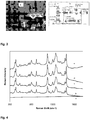
- An external view of the microscope (a) and its schematic diagram (b) are shown in Fig. 3 .
- Fig. 4 shows four randomly selected spectra of malachite green adsorbed on the surface of the substrate (b, c, d, e) and the spectrum of the substrate itself (a) ( Fig. 4 ). The spectra were recorded during 10s, using a 785nm excitation with power of 2.5mW.
- the spectra recorded at different points of the substrate are identical. They include strong bands at frequencies: 1618, 1370, 1180 and 441cm -1 , whereas the relative intensities in each recorded spectrum are virtually the same.
- N SERS has been estimated based on a surface coverage with malachite green (1x10 14 molecules/cm 2 ) [ B. Pettinger, B. Ren, G. Picardi, R. Schuster, G.. Ertl, J. Raman Spectrosc. Volume 36 Issue 6-7, Pages 541- 550 ].
- N Raman denotes the number of malachite green molecules in solution under study calculated with the definitions given above.
- the estimated enhancement factor (EF) for malachite green is 2.6x10 6 and is by two orders of magnitude higher than the enhancement factor estimated on a commercially available SERS substrate.
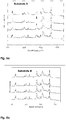
- p-aminothiophenol molecules have been adsorbed on a SERS platform and the reproducibility of collected spectra has been tested for the same surface and for two different surfaces ( Fig. 6 and 7 ).
- the light wavelength used in measurements was 785nm, the laser power at the sample was 3mW and the spectrum accumulation time was about 10s.
- the spectra of p-aminothiophenol molecules adsorbed on a SERS substrate from a 10 -4 M aqueous p-aminothiophenol solution recorded at different points of the surface are reproducible ( Fig. 6 ).
- Relative intensities of the bands characteristic for p-aminothiophenol at 840cm -1 , 1080cm -1 and 1589cm -1 are reproducible to 80% for all recorded spectra.
- the frequencies and relative intensities of p-aminothiophenol bands are reproducible for four different SERS substrates fabricated with the same method according to the invention ( Fig. 7 ).
- the reproducibility of frequencies and relative band intensities is higher than 75% for four substrates A, B, C and D ( Fig. 7 ) fabricated according to the invention.
- I SERS and I Raman have been estimated for the most intense band appearing at frequency 1589cm -1 ascribed to a v 8a vibration of the p-aminothiophenol aromatic ring in SERS and in normal Raman spectrum, respectively.
- the normal Raman spectrum was recorded for a 10mM aqueous p-aminothiophenol solution, using 785nm excitation line and laser power 150mW.
- N SERS and N Raman correspond to the numbers of molecules excited with laser beam during SERS measurements and during recording normal Raman spectrum in p-aminothiophenol solution.
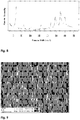
- a 10 -4 M aqueous solution of L-alanine were placed on a SERS substrate according to the embodiment 1 and after the substrate had been dried, the SERS have been recorded ( Fig. 8 ).
- the spectra were recorded with a 785nm excitation, the laser power was 10mW, and the spectrum accumulation time was 5 minutes ( Fig. 8 ).
- the estimated enhancement factor (EF) for L-alanine was 1.9x10 4 .
- the substrate according to the invention is characterised by a high enhancement factor of the order 10 6 and a very good reproducibility of recorded spectra both for one (not less than 80%) and for several substrates (not less than 75%).
- a substrate according to the invention can be used for SERS studies of a broad range of chemical compounds (e.g., organic compounds including dyes, peptides, natural organic compounds present in live cells, as for instance phenylalanine or DNA, biologically active substances and biological processes, such as for instance in studies on neurotransmitters including catechol, dopamine, epinephrine, nucleotides, nucleosides, membranes and cytochromes).
- the subject matter of the invention can be also dedicated to the detection and characterisation of viruses, drug interactions with proteins or posttranslational modifications. Due to the properties mentioned above the subject matter of the invention can be used as an active platform in biosensor design, making SERS technique a useful analytical tool in medical diagnostics.
Landscapes
- Health & Medical Sciences (AREA)
- Chemical & Material Sciences (AREA)
- Physics & Mathematics (AREA)
- General Health & Medical Sciences (AREA)
- Life Sciences & Earth Sciences (AREA)
- General Physics & Mathematics (AREA)
- Engineering & Computer Science (AREA)
- Nanotechnology (AREA)
- Biochemistry (AREA)
- Analytical Chemistry (AREA)
- Nuclear Medicine, Radiotherapy & Molecular Imaging (AREA)
- Immunology (AREA)
- Pathology (AREA)
- Spectroscopy & Molecular Physics (AREA)
- Molecular Biology (AREA)
- Crystallography & Structural Chemistry (AREA)
- Investigating, Analyzing Materials By Fluorescence Or Luminescence (AREA)
- Crystals, And After-Treatments Of Crystals (AREA)
Claims (15)
- Ein Substrat für oberflächenverstärkte Ramanstreuungsstudien, basierend auf einer Oberfläche eines galliumhaltigen Nitrids enthaltend die Whiskers des genannten galliumhaltigen Nitrid, wobei die Whiskers mit Metall ausgewählt aus der Gruppe bestehend aus Silber, Gold, Platin, Kupfer und/oder deren Legierungen beschichtet sind, worin
im Wesentlichen jeder Whisker innerhalb einen linearen Defekt enthält. - Substrat nach Anspruch 1, wobei die erwähnten Whiskers miteinander durch Anschlüsse verbunden sind, die von der erwähnten galliumhaltigen Nitridoberfläche entfernt sind,
die die konische Bündel bilden. - Substrat nach Anspruch 1 oder 2, wobei der genannte lineare Defekt eine Dislokations- oder eine Inversionsdomäne ist.
- Substrat nach einem der vorhergehenden Ansprüche, wobei die Filmdicke des auf der genannten galliumhaltigen Nitridoberfläche erwähnten Metalls
im Bereich von 50 nm bis 150 nm, bevorzugt von 70 nm bis 80 nm, liegt. - Substrat nach einem der vorhergehenden Ansprüche, wobei die Länge
der erwähnten Whiskers im Bereich von 0,2 µm bis 2,0 µm, bevorzugter von 0,5 µm bis 1,5 µm, liegt - Substrat nach einem der vorhergehenden Ansprüche, wobei der Durchmesser der erwähnten Whiskers im Bereich von 40 nm bis 150 nm, bevorzugter von 50 nm bis 70 nm, liegt.
- Substrat nach einem der vorhergehenden Ansprüche, wobei das Verhältnis von Länge zu Durchmesser der erwähnten Whiskers im Bereich von 5 bis 50, bevorzugter von 10 bis 30, liegt.
- Substrat nach einem der vorhergehenden Ansprüche, wobei die Oberflächendichte der Whiskers auf der erwähnten galliumhaltigen Nitridoberfläche im Bereich von 108/cm2 bis 1010/cm2 liegt.
- Substrat nach einem der vorhergehenden Ansprüche, wobei das erwähnte Metall Gold ist.
- Substrat nach einem der vorhergehenden Ansprüche, wobei das erwähnte galliumhaltige Nitrid Galliumnitrid GaN ist.
- Substrat nach Anspruch 10, wobei die erwähnte Galliumnitridoberfläche eine Oberfläche, die einer kristallographischen Ebene mit Miller-Indizes (0001) ähnlich ist, d.h. die kristallographische Ebene C mit Ga-Polarität ist.
- Substrat nach Anspruch 10, wobei die erwähnte Galliumnitridoberfläche eine Oberfläche, die einer kristallographischen Ebene mit Miller-Indizes (000-1) ähnlich ist, d.h. die kristallographische Ebene C mit N-Polarität ist.
- Substrat nach einem der vorhergehenden Ansprüche, wobei für Moleküle, die an seiner Oberfläche adsorbiert sind, der Verstärkungsfaktor, EF, höher als 104 und bevorzugter höher als 106 ist.
- Substrat nach einem der vorhergehenden Ansprüche, wobei die Reproduzierbarkeit von Raman-Spektren, die an verschiedenen Punkten des gleichen Substrats aufgenommnen werden, nicht weniger als 80% beträgt.
- Substrat nach einem der vorhergehenden Ansprüche, wobei die Reproduzierbarkeit von Raman-Spektren, die an verschiedenen erwähnten Substraten aufgenommnen werden, nicht weniger als 75% beträgt.
Applications Claiming Priority (1)
| Application Number | Priority Date | Filing Date | Title |
|---|---|---|---|
| PL390798A PL219706B1 (pl) | 2010-03-23 | 2010-03-23 | Platforma do pomiarów powierzchniowo wzmocnionego efektu Ramana |
Publications (3)
| Publication Number | Publication Date |
|---|---|
| EP2369327A2 EP2369327A2 (de) | 2011-09-28 |
| EP2369327A3 EP2369327A3 (de) | 2011-12-21 |
| EP2369327B1 true EP2369327B1 (de) | 2018-05-23 |
Family
ID=44209941
Family Applications (1)
| Application Number | Title | Priority Date | Filing Date |
|---|---|---|---|
| EP11159330.7A Not-in-force EP2369327B1 (de) | 2010-03-23 | 2011-03-23 | Substrat für oberflächenverstärkte Raman-Streuung |
Country Status (7)
| Country | Link |
|---|---|
| US (1) | US8531660B2 (de) |
| EP (1) | EP2369327B1 (de) |
| JP (1) | JP2011201769A (de) |
| KR (1) | KR20110106821A (de) |
| CN (1) | CN102213677A (de) |
| PL (1) | PL219706B1 (de) |
| UA (1) | UA109104C2 (de) |
Families Citing this family (19)
| Publication number | Priority date | Publication date | Assignee | Title |
|---|---|---|---|---|
| CN102677212B (zh) * | 2012-06-01 | 2013-11-13 | 苏州大学 | 一种表面增强拉曼散射活性基底及其制备方法 |
| TWI604186B (zh) | 2012-08-10 | 2017-11-01 | Hamamatsu Photonics Kk | Surface Enhanced Raman Scattering Element |
| CN104520694B (zh) | 2012-08-10 | 2018-05-15 | 浜松光子学株式会社 | 表面增强拉曼散射单元及其使用方法 |
| WO2014025034A1 (ja) | 2012-08-10 | 2014-02-13 | 浜松ホトニクス株式会社 | 表面増強ラマン散乱ユニット |
| US9863884B2 (en) | 2012-08-10 | 2018-01-09 | Hamamatsu Photonics K.K. | Surface-enhanced Raman scattering element, and method for producing same |
| KR101412420B1 (ko) * | 2012-10-04 | 2014-07-01 | 연세대학교 산학협력단 | 표면증강 라만 산란 센서 및 그 센싱방법 |
| KR101589039B1 (ko) | 2013-05-30 | 2016-01-27 | 한국과학기술원 | 대면적 금속 나노 구조물 및 투명전극층을 포함하는 표면증강라만산란 기판, 이의 제조방법 및 이를 이용한 표면증강라만 분광방법 |
| CN105004706B (zh) * | 2014-04-24 | 2018-05-29 | 中国科学院苏州纳米技术与纳米仿生研究所 | 表面增强拉曼散射活性基底及其制备方法 |
| CN106323936B (zh) * | 2015-07-07 | 2019-09-10 | 中国科学院苏州纳米技术与纳米仿生研究所 | 一种采用紫外激光拉曼光谱检测GaN材料的方法 |
| CN107727633B (zh) * | 2017-09-20 | 2020-10-30 | 复旦大学 | 一种表面增强拉曼光谱检测平台及其制备方法与应用 |
| CN108275651A (zh) * | 2018-01-22 | 2018-07-13 | 临沂大学 | 一种表面增强拉曼散射基底的制备方法 |
| US10761049B2 (en) * | 2018-09-26 | 2020-09-01 | United Arab Emirates University | Nitride based sensor |
| CN110534384B (zh) * | 2019-07-26 | 2020-07-17 | 宁波工程学院 | 一种Au纳米颗粒修饰枝状TiO2纳米棒阵列作为场发射阴极材料的应用 |
| CN110426384A (zh) * | 2019-08-09 | 2019-11-08 | 中国科学院苏州纳米技术与纳米仿生研究所 | 烯烃单体中4-叔丁基邻苯二酚的特异性检测方法 |
| CN111122634A (zh) * | 2019-12-25 | 2020-05-08 | 同济大学 | 基于扫描电镜-拉曼技术鉴定水溶液中纳米塑料颗粒的方法 |
| CN111679350B (zh) * | 2020-06-24 | 2021-04-20 | 江南大学 | 一种等离子金属-半导体复合膜及其制备方法与其在非食用色素检测中的应用 |
| CN112268888A (zh) * | 2020-10-19 | 2021-01-26 | 西安工程大学 | 一种银纳米线-氮化镓纳米颗粒复合材料的制备方法 |
| KR102414417B1 (ko) * | 2021-01-06 | 2022-06-28 | 가천대학교 산학협력단 | 다공성 실리콘 및 금속 나노입자를 포함하는 다공성 실리콘 나노센서 및 그의 제조방법 |
| CN113667138B (zh) * | 2021-09-28 | 2023-03-14 | 上海师范大学 | 银-金-金属有机框架复合物表面增强拉曼散射基底及其制备方法和应用 |
Family Cites Families (14)
| Publication number | Priority date | Publication date | Assignee | Title |
|---|---|---|---|---|
| PL183687B1 (pl) * | 1997-06-06 | 2002-06-28 | Ct Badan | Sposób wytwarzania półprzewodnikowych związków grupy A-B o przewodnictwie elektrycznym typu p i typu n |
| EP1613549B1 (de) * | 2003-04-04 | 2013-08-07 | QuNano AB | Präzise positionierte nanowhiskern strukturen und verfahren zu ihrer herstellung |
| US7583379B2 (en) * | 2005-07-28 | 2009-09-01 | University Of Georgia Research Foundation | Surface enhanced raman spectroscopy (SERS) systems and methods of use thereof |
| US7595872B2 (en) * | 2004-12-03 | 2009-09-29 | Trustees Of Boston University | Analyzer for nanostructured substrate for surface enhanced Raman scattering |
| US8129199B2 (en) * | 2004-12-13 | 2012-03-06 | University of South Caroliina | Surface enhanced Raman spectroscopy using shaped gold nanoparticles |
| US20060275541A1 (en) * | 2005-06-07 | 2006-12-07 | Weimer Wayne A | Systems and method for fabricating substrate surfaces for SERS and apparatuses utilizing same |
| US7586601B2 (en) * | 2005-06-14 | 2009-09-08 | Ebstein Steven M | Applications of laser-processed substrate for molecular diagnostics |
| US7715003B2 (en) * | 2005-06-14 | 2010-05-11 | President & Fellows Of Harvard College | Metalized semiconductor substrates for raman spectroscopy |
| US8184284B2 (en) * | 2005-06-14 | 2012-05-22 | Ebstein Steven M | Laser-processed substrate for molecular diagnostics |
| US7426025B2 (en) * | 2005-09-23 | 2008-09-16 | Hewlett-Packard Development Company, L.P. | Nanostructures, systems, and methods including nanolasers for enhanced Raman spectroscopy |
| US20100171948A1 (en) * | 2006-06-14 | 2010-07-08 | President And Fellows Of Harvard College | Metalized semiconductor substrates for raman spectroscopy |
| WO2008094089A1 (en) | 2007-01-29 | 2008-08-07 | Nanexa Ab | Active sensor surface and a method for manufacture thereof |
| US7639356B2 (en) | 2007-05-18 | 2009-12-29 | The United States Of America As Represented By The Secretary Of The Navy | Highly efficient surface enhanced Raman and fluorescence nanostructure substrates |
| US20100190661A1 (en) * | 2009-01-26 | 2010-07-29 | City University Of Hong Kong | Sers-active structure for use in raman spectroscopy |
-
2010
- 2010-03-23 PL PL390798A patent/PL219706B1/pl unknown
-
2011
- 2011-03-09 UA UAA201102774A patent/UA109104C2/uk unknown
- 2011-03-18 US US13/051,618 patent/US8531660B2/en active Active
- 2011-03-21 CN CN2011100715157A patent/CN102213677A/zh active Pending
- 2011-03-22 KR KR1020110025571A patent/KR20110106821A/ko not_active Ceased
- 2011-03-22 JP JP2011062201A patent/JP2011201769A/ja not_active Withdrawn
- 2011-03-23 EP EP11159330.7A patent/EP2369327B1/de not_active Not-in-force
Non-Patent Citations (1)
| Title |
|---|
| None * |
Also Published As
| Publication number | Publication date |
|---|---|
| UA109104C2 (uk) | 2015-07-27 |
| EP2369327A3 (de) | 2011-12-21 |
| US20110235031A1 (en) | 2011-09-29 |
| KR20110106821A (ko) | 2011-09-29 |
| EP2369327A2 (de) | 2011-09-28 |
| US8531660B2 (en) | 2013-09-10 |
| PL390798A1 (pl) | 2011-09-26 |
| JP2011201769A (ja) | 2011-10-13 |
| PL219706B1 (pl) | 2015-06-30 |
| RU2011110372A (ru) | 2012-10-27 |
| CN102213677A (zh) | 2011-10-12 |
Similar Documents
| Publication | Publication Date | Title |
|---|---|---|
| EP2369327A2 (de) | Substrat für oberflächenverstärkte Raman-Streuung | |
| Das et al. | Nano-patterned SERS substrate: Application for protein analysis vs. temperature | |
| Weyher et al. | Relationship between the nano-structure of GaN surfaces and SERS efficiency: Chasing hot-spots | |
| Liu et al. | Trace detection of cyanide based on SERS effect of Ag nanoplate-built hollow microsphere arrays | |
| Siddhanta et al. | Universal metal-semiconductor hybrid nanostructured SERS substrate for biosensing | |
| Hammad et al. | Improving SERS substrates with Au/Ag-coated Si nanostructures generated by laser ablation synthesis in PVA | |
| Wagner et al. | Towards multi-molecular surface-enhanced infrared absorption using metal plasmonics | |
| Wang et al. | Silicon nanowire based single-molecule SERS sensor | |
| Krajczewski et al. | New, epitaxial approach to SERS platform preparation–InP nanowires coated by an Au layer as a new, highly active, and stable SERS platform | |
| Le Thi Minh et al. | Conductivity support of AZO in enhancements of SERS Ag/AZO substrate to detect ketoprofen | |
| Liu et al. | Tunable and highly reproducible surface-enhanced Raman scattering substrates made from large-scale nanoparticle arrays based on periodically poled LiNbO3 templates | |
| Yang et al. | Plasmon-free surface-enhanced raman spectroscopy using α-type MoO3 semiconductor nanorods with strong light scattering in the visible regime | |
| Li et al. | Assembling PVP-Au NPs as portable chip for sensitive detection of cyanide with surface-enhanced Raman spectroscopy | |
| Huang et al. | Electrochemically fabricated self-aligned 2-D silver/alumina arrays as reliable SERS sensors | |
| Dhawan et al. | Methodologies for developing surface-enhanced Raman scattering (SERS) substrates for detection of chemical and biological molecules | |
| Dong et al. | Polymer-single-crystal@ nanoparticle nanosandwich for surface enhanced Raman spectroscopy | |
| Chantaraklud et al. | Light-driven in situ deposited Au nanoparticles on ZnO substrate with ultrasensitive SERS enhancement for molecular detection | |
| Dhar Dwivedi et al. | Detection technique for vitamin D3 using Er-doped TiO2 nanowire-based UV photodetector | |
| CN112014371B (zh) | 一种柔性半透明表面增强拉曼基底的制备方法及应用 | |
| Xu et al. | High surface roughness gold nanoparticle/centimeter level silver nanowire heterostructure detectors for SERS application | |
| Jose et al. | Regio-selective decoration of nanocavity metal arrays: contributions from localized and delocalized plasmons to surface enhanced Raman spectroscopy | |
| RU2574176C2 (ru) | Подложка для исследований методом усиленного поверхностью комбинационного рассеяния | |
| Jradi et al. | Femtosecond Direct Laser-Induced Assembly of Monolayer of Gold Nanostructures with Tunable Surface Plasmon Resonance and High Performance Localized Surface Plasmon Resonance and Surface Enhanced Raman Scattering Sensing | |
| Konstantinova et al. | Application of quantum dots CdZnSeS/ZnS luminescence, enhanced by plasmons of silver rough surface for detection of albumin in blood facies of infected person | |
| Li et al. | Influence of Chiral-Related Selective Adsorbed Oxygen on the Fluorescence Interaction between CdTe Quantum Dots and Folic Acid |
Legal Events
| Date | Code | Title | Description |
|---|---|---|---|
| PUAI | Public reference made under article 153(3) epc to a published international application that has entered the european phase |
Free format text: ORIGINAL CODE: 0009012 |
|
| AK | Designated contracting states |
Kind code of ref document: A2 Designated state(s): AL AT BE BG CH CY CZ DE DK EE ES FI FR GB GR HR HU IE IS IT LI LT LU LV MC MK MT NL NO PL PT RO RS SE SI SK SM TR |
|
| AX | Request for extension of the european patent |
Extension state: BA ME |
|
| RAP1 | Party data changed (applicant data changed or rights of an application transferred) |
Owner name: INSTYTUT CHEMII FIZYCZNEJ POLSKIEJ AKADEMII NAUK Owner name: INSTYTUT WYSOKICH CISNIEN POLSKIEJ AKADEMII NAUK |
|
| PUAL | Search report despatched |
Free format text: ORIGINAL CODE: 0009013 |
|
| AK | Designated contracting states |
Kind code of ref document: A3 Designated state(s): AL AT BE BG CH CY CZ DE DK EE ES FI FR GB GR HR HU IE IS IT LI LT LU LV MC MK MT NL NO PL PT RO RS SE SI SK SM TR |
|
| AX | Request for extension of the european patent |
Extension state: BA ME |
|
| RIC1 | Information provided on ipc code assigned before grant |
Ipc: G01N 21/65 20060101AFI20111111BHEP Ipc: B82Y 15/00 20110101ALI20111111BHEP |
|
| 17P | Request for examination filed |
Effective date: 20120615 |
|
| GRAP | Despatch of communication of intention to grant a patent |
Free format text: ORIGINAL CODE: EPIDOSNIGR1 |
|
| STAA | Information on the status of an ep patent application or granted ep patent |
Free format text: STATUS: GRANT OF PATENT IS INTENDED |
|
| INTG | Intention to grant announced |
Effective date: 20171128 |
|
| GRAS | Grant fee paid |
Free format text: ORIGINAL CODE: EPIDOSNIGR3 |
|
| GRAA | (expected) grant |
Free format text: ORIGINAL CODE: 0009210 |
|
| STAA | Information on the status of an ep patent application or granted ep patent |
Free format text: STATUS: THE PATENT HAS BEEN GRANTED |
|
| AK | Designated contracting states |
Kind code of ref document: B1 Designated state(s): AL AT BE BG CH CY CZ DE DK EE ES FI FR GB GR HR HU IE IS IT LI LT LU LV MC MK MT NL NO PL PT RO RS SE SI SK SM TR |
|
| REG | Reference to a national code |
Ref country code: GB Ref legal event code: FG4D |
|
| REG | Reference to a national code |
Ref country code: CH Ref legal event code: EP |
|
| REG | Reference to a national code |
Ref country code: IE Ref legal event code: FG4D |
|
| REG | Reference to a national code |
Ref country code: AT Ref legal event code: REF Ref document number: 1001910 Country of ref document: AT Kind code of ref document: T Effective date: 20180615 |
|
| REG | Reference to a national code |
Ref country code: DE Ref legal event code: R096 Ref document number: 602011048523 Country of ref document: DE |
|
| REG | Reference to a national code |
Ref country code: NL Ref legal event code: MP Effective date: 20180523 |
|
| REG | Reference to a national code |
Ref country code: LT Ref legal event code: MG4D |
|
| PG25 | Lapsed in a contracting state [announced via postgrant information from national office to epo] |
Ref country code: BG Free format text: LAPSE BECAUSE OF FAILURE TO SUBMIT A TRANSLATION OF THE DESCRIPTION OR TO PAY THE FEE WITHIN THE PRESCRIBED TIME-LIMIT Effective date: 20180823 Ref country code: NO Free format text: LAPSE BECAUSE OF FAILURE TO SUBMIT A TRANSLATION OF THE DESCRIPTION OR TO PAY THE FEE WITHIN THE PRESCRIBED TIME-LIMIT Effective date: 20180823 Ref country code: FI Free format text: LAPSE BECAUSE OF FAILURE TO SUBMIT A TRANSLATION OF THE DESCRIPTION OR TO PAY THE FEE WITHIN THE PRESCRIBED TIME-LIMIT Effective date: 20180523 Ref country code: SE Free format text: LAPSE BECAUSE OF FAILURE TO SUBMIT A TRANSLATION OF THE DESCRIPTION OR TO PAY THE FEE WITHIN THE PRESCRIBED TIME-LIMIT Effective date: 20180523 Ref country code: LT Free format text: LAPSE BECAUSE OF FAILURE TO SUBMIT A TRANSLATION OF THE DESCRIPTION OR TO PAY THE FEE WITHIN THE PRESCRIBED TIME-LIMIT Effective date: 20180523 Ref country code: ES Free format text: LAPSE BECAUSE OF FAILURE TO SUBMIT A TRANSLATION OF THE DESCRIPTION OR TO PAY THE FEE WITHIN THE PRESCRIBED TIME-LIMIT Effective date: 20180523 |
|
| PG25 | Lapsed in a contracting state [announced via postgrant information from national office to epo] |
Ref country code: HR Free format text: LAPSE BECAUSE OF FAILURE TO SUBMIT A TRANSLATION OF THE DESCRIPTION OR TO PAY THE FEE WITHIN THE PRESCRIBED TIME-LIMIT Effective date: 20180523 Ref country code: RS Free format text: LAPSE BECAUSE OF FAILURE TO SUBMIT A TRANSLATION OF THE DESCRIPTION OR TO PAY THE FEE WITHIN THE PRESCRIBED TIME-LIMIT Effective date: 20180523 Ref country code: NL Free format text: LAPSE BECAUSE OF FAILURE TO SUBMIT A TRANSLATION OF THE DESCRIPTION OR TO PAY THE FEE WITHIN THE PRESCRIBED TIME-LIMIT Effective date: 20180523 Ref country code: GR Free format text: LAPSE BECAUSE OF FAILURE TO SUBMIT A TRANSLATION OF THE DESCRIPTION OR TO PAY THE FEE WITHIN THE PRESCRIBED TIME-LIMIT Effective date: 20180824 Ref country code: LV Free format text: LAPSE BECAUSE OF FAILURE TO SUBMIT A TRANSLATION OF THE DESCRIPTION OR TO PAY THE FEE WITHIN THE PRESCRIBED TIME-LIMIT Effective date: 20180523 |
|
| REG | Reference to a national code |
Ref country code: AT Ref legal event code: MK05 Ref document number: 1001910 Country of ref document: AT Kind code of ref document: T Effective date: 20180523 |
|
| PG25 | Lapsed in a contracting state [announced via postgrant information from national office to epo] |
Ref country code: SK Free format text: LAPSE BECAUSE OF FAILURE TO SUBMIT A TRANSLATION OF THE DESCRIPTION OR TO PAY THE FEE WITHIN THE PRESCRIBED TIME-LIMIT Effective date: 20180523 Ref country code: RO Free format text: LAPSE BECAUSE OF FAILURE TO SUBMIT A TRANSLATION OF THE DESCRIPTION OR TO PAY THE FEE WITHIN THE PRESCRIBED TIME-LIMIT Effective date: 20180523 Ref country code: CZ Free format text: LAPSE BECAUSE OF FAILURE TO SUBMIT A TRANSLATION OF THE DESCRIPTION OR TO PAY THE FEE WITHIN THE PRESCRIBED TIME-LIMIT Effective date: 20180523 Ref country code: DK Free format text: LAPSE BECAUSE OF FAILURE TO SUBMIT A TRANSLATION OF THE DESCRIPTION OR TO PAY THE FEE WITHIN THE PRESCRIBED TIME-LIMIT Effective date: 20180523 Ref country code: AT Free format text: LAPSE BECAUSE OF FAILURE TO SUBMIT A TRANSLATION OF THE DESCRIPTION OR TO PAY THE FEE WITHIN THE PRESCRIBED TIME-LIMIT Effective date: 20180523 Ref country code: EE Free format text: LAPSE BECAUSE OF FAILURE TO SUBMIT A TRANSLATION OF THE DESCRIPTION OR TO PAY THE FEE WITHIN THE PRESCRIBED TIME-LIMIT Effective date: 20180523 Ref country code: PL Free format text: LAPSE BECAUSE OF FAILURE TO SUBMIT A TRANSLATION OF THE DESCRIPTION OR TO PAY THE FEE WITHIN THE PRESCRIBED TIME-LIMIT Effective date: 20180523 |
|
| REG | Reference to a national code |
Ref country code: DE Ref legal event code: R097 Ref document number: 602011048523 Country of ref document: DE |
|
| PG25 | Lapsed in a contracting state [announced via postgrant information from national office to epo] |
Ref country code: SM Free format text: LAPSE BECAUSE OF FAILURE TO SUBMIT A TRANSLATION OF THE DESCRIPTION OR TO PAY THE FEE WITHIN THE PRESCRIBED TIME-LIMIT Effective date: 20180523 Ref country code: IT Free format text: LAPSE BECAUSE OF FAILURE TO SUBMIT A TRANSLATION OF THE DESCRIPTION OR TO PAY THE FEE WITHIN THE PRESCRIBED TIME-LIMIT Effective date: 20180523 |
|
| PLBE | No opposition filed within time limit |
Free format text: ORIGINAL CODE: 0009261 |
|
| STAA | Information on the status of an ep patent application or granted ep patent |
Free format text: STATUS: NO OPPOSITION FILED WITHIN TIME LIMIT |
|
| 26N | No opposition filed |
Effective date: 20190226 |
|
| PG25 | Lapsed in a contracting state [announced via postgrant information from national office to epo] |
Ref country code: SI Free format text: LAPSE BECAUSE OF FAILURE TO SUBMIT A TRANSLATION OF THE DESCRIPTION OR TO PAY THE FEE WITHIN THE PRESCRIBED TIME-LIMIT Effective date: 20180523 |
|
| REG | Reference to a national code |
Ref country code: DE Ref legal event code: R119 Ref document number: 602011048523 Country of ref document: DE |
|
| PG25 | Lapsed in a contracting state [announced via postgrant information from national office to epo] |
Ref country code: MC Free format text: LAPSE BECAUSE OF FAILURE TO SUBMIT A TRANSLATION OF THE DESCRIPTION OR TO PAY THE FEE WITHIN THE PRESCRIBED TIME-LIMIT Effective date: 20180523 |
|
| REG | Reference to a national code |
Ref country code: CH Ref legal event code: PL |
|
| GBPC | Gb: european patent ceased through non-payment of renewal fee |
Effective date: 20190323 |
|
| PG25 | Lapsed in a contracting state [announced via postgrant information from national office to epo] |
Ref country code: AL Free format text: LAPSE BECAUSE OF FAILURE TO SUBMIT A TRANSLATION OF THE DESCRIPTION OR TO PAY THE FEE WITHIN THE PRESCRIBED TIME-LIMIT Effective date: 20180523 Ref country code: LU Free format text: LAPSE BECAUSE OF NON-PAYMENT OF DUE FEES Effective date: 20190323 |
|
| REG | Reference to a national code |
Ref country code: BE Ref legal event code: MM Effective date: 20190331 |
|
| PG25 | Lapsed in a contracting state [announced via postgrant information from national office to epo] |
Ref country code: IE Free format text: LAPSE BECAUSE OF NON-PAYMENT OF DUE FEES Effective date: 20190323 Ref country code: CH Free format text: LAPSE BECAUSE OF NON-PAYMENT OF DUE FEES Effective date: 20190331 Ref country code: DE Free format text: LAPSE BECAUSE OF NON-PAYMENT OF DUE FEES Effective date: 20191001 Ref country code: GB Free format text: LAPSE BECAUSE OF NON-PAYMENT OF DUE FEES Effective date: 20190323 Ref country code: LI Free format text: LAPSE BECAUSE OF NON-PAYMENT OF DUE FEES Effective date: 20190331 |
|
| PG25 | Lapsed in a contracting state [announced via postgrant information from national office to epo] |
Ref country code: FR Free format text: LAPSE BECAUSE OF NON-PAYMENT OF DUE FEES Effective date: 20190331 Ref country code: BE Free format text: LAPSE BECAUSE OF NON-PAYMENT OF DUE FEES Effective date: 20190331 |
|
| PG25 | Lapsed in a contracting state [announced via postgrant information from national office to epo] |
Ref country code: TR Free format text: LAPSE BECAUSE OF FAILURE TO SUBMIT A TRANSLATION OF THE DESCRIPTION OR TO PAY THE FEE WITHIN THE PRESCRIBED TIME-LIMIT Effective date: 20180523 |
|
| PG25 | Lapsed in a contracting state [announced via postgrant information from national office to epo] |
Ref country code: MT Free format text: LAPSE BECAUSE OF NON-PAYMENT OF DUE FEES Effective date: 20190323 Ref country code: PT Free format text: LAPSE BECAUSE OF FAILURE TO SUBMIT A TRANSLATION OF THE DESCRIPTION OR TO PAY THE FEE WITHIN THE PRESCRIBED TIME-LIMIT Effective date: 20180924 |
|
| PG25 | Lapsed in a contracting state [announced via postgrant information from national office to epo] |
Ref country code: CY Free format text: LAPSE BECAUSE OF FAILURE TO SUBMIT A TRANSLATION OF THE DESCRIPTION OR TO PAY THE FEE WITHIN THE PRESCRIBED TIME-LIMIT Effective date: 20180523 |
|
| PG25 | Lapsed in a contracting state [announced via postgrant information from national office to epo] |
Ref country code: IS Free format text: LAPSE BECAUSE OF FAILURE TO SUBMIT A TRANSLATION OF THE DESCRIPTION OR TO PAY THE FEE WITHIN THE PRESCRIBED TIME-LIMIT Effective date: 20180923 |
|
| PG25 | Lapsed in a contracting state [announced via postgrant information from national office to epo] |
Ref country code: HU Free format text: LAPSE BECAUSE OF FAILURE TO SUBMIT A TRANSLATION OF THE DESCRIPTION OR TO PAY THE FEE WITHIN THE PRESCRIBED TIME-LIMIT; INVALID AB INITIO Effective date: 20110323 |
|
| PG25 | Lapsed in a contracting state [announced via postgrant information from national office to epo] |
Ref country code: MK Free format text: LAPSE BECAUSE OF FAILURE TO SUBMIT A TRANSLATION OF THE DESCRIPTION OR TO PAY THE FEE WITHIN THE PRESCRIBED TIME-LIMIT Effective date: 20180523 |