EP2342772B1 - Organisches elektronisches bauelement und verfahren zu dessen herstellung - Google Patents
Organisches elektronisches bauelement und verfahren zu dessen herstellung Download PDFInfo
- Publication number
- EP2342772B1 EP2342772B1 EP09741205.0A EP09741205A EP2342772B1 EP 2342772 B1 EP2342772 B1 EP 2342772B1 EP 09741205 A EP09741205 A EP 09741205A EP 2342772 B1 EP2342772 B1 EP 2342772B1
- Authority
- EP
- European Patent Office
- Prior art keywords
- electron
- organic
- organic compound
- layer
- metal complex
- Prior art date
- Legal status (The legal status is an assumption and is not a legal conclusion. Google has not performed a legal analysis and makes no representation as to the accuracy of the status listed.)
- Active
Links
Images


Classifications
-
- H—ELECTRICITY
- H10—SEMICONDUCTOR DEVICES; ELECTRIC SOLID-STATE DEVICES NOT OTHERWISE PROVIDED FOR
- H10K—ORGANIC ELECTRIC SOLID-STATE DEVICES
- H10K85/00—Organic materials used in the body or electrodes of devices covered by this subclass
- H10K85/60—Organic compounds having low molecular weight
- H10K85/649—Aromatic compounds comprising a hetero atom
- H10K85/654—Aromatic compounds comprising a hetero atom comprising only nitrogen as heteroatom
-
- H—ELECTRICITY
- H10—SEMICONDUCTOR DEVICES; ELECTRIC SOLID-STATE DEVICES NOT OTHERWISE PROVIDED FOR
- H10K—ORGANIC ELECTRIC SOLID-STATE DEVICES
- H10K50/00—Organic light-emitting devices
-
- H—ELECTRICITY
- H10—SEMICONDUCTOR DEVICES; ELECTRIC SOLID-STATE DEVICES NOT OTHERWISE PROVIDED FOR
- H10K—ORGANIC ELECTRIC SOLID-STATE DEVICES
- H10K85/00—Organic materials used in the body or electrodes of devices covered by this subclass
- H10K85/30—Coordination compounds
- H10K85/361—Polynuclear complexes, i.e. complexes comprising two or more metal centers
-
- H—ELECTRICITY
- H10—SEMICONDUCTOR DEVICES; ELECTRIC SOLID-STATE DEVICES NOT OTHERWISE PROVIDED FOR
- H10K—ORGANIC ELECTRIC SOLID-STATE DEVICES
- H10K85/00—Organic materials used in the body or electrodes of devices covered by this subclass
- H10K85/60—Organic compounds having low molecular weight
- H10K85/649—Aromatic compounds comprising a hetero atom
- H10K85/657—Polycyclic condensed heteroaromatic hydrocarbons
- H10K85/6572—Polycyclic condensed heteroaromatic hydrocarbons comprising only nitrogen in the heteroaromatic polycondensed ring system, e.g. phenanthroline or carbazole
-
- H—ELECTRICITY
- H10—SEMICONDUCTOR DEVICES; ELECTRIC SOLID-STATE DEVICES NOT OTHERWISE PROVIDED FOR
- H10K—ORGANIC ELECTRIC SOLID-STATE DEVICES
- H10K10/00—Organic devices specially adapted for rectifying, amplifying, oscillating or switching; Organic capacitors or resistors having potential barriers
- H10K10/40—Organic transistors
- H10K10/46—Field-effect transistors, e.g. organic thin-film transistors [OTFT]
-
- H—ELECTRICITY
- H10—SEMICONDUCTOR DEVICES; ELECTRIC SOLID-STATE DEVICES NOT OTHERWISE PROVIDED FOR
- H10K—ORGANIC ELECTRIC SOLID-STATE DEVICES
- H10K50/00—Organic light-emitting devices
- H10K50/10—OLEDs or polymer light-emitting diodes [PLED]
- H10K50/14—Carrier transporting layers
Definitions
- An organic electronic component according to claim 1 is specified.
- a common problem in organic electronic devices is to provide a layer that has very high electron conductivity.
- the electronic conductivity in the device is often the determining factor for the efficiency and lifetime of the device.
- OLED organic LED
- excitons are formed by the recombination of electrons and holes, which can excite substances for the emission of radiation.
- the luminescence also depends directly on the density of the exciton, which in turn depends on the recombination of electrons and holes.
- purely crystalline layers are used for electron transport. These purely crystalline layers have the disadvantage that they have regions of different conductivity. This has the consequence that the charge carriers always choose the path of the smallest resistance. This leads to uneven electron flow in this layer. At the points where a significantly increased flow of electrons occurs, overheating of the layer can occur and thus damage.
- this unequal electron flow furthermore leads to an inhomogeneous emission.
- the device In areas where a higher electron flow occurs and multiple excitons are formed, the device emits more radiation and is therefore brighter than in areas where there is a low electron flux.
- a low operating voltage light emitting element having an electron transport layer obtained by coevaporating a matrix material such as Alq 3 with additives.
- a mixed layer is obtained by co-depositing an electron-transporting organic compound with an organometallic complex.
- WO 2004/015746 it is described that a layer of [Ru (2,2 ', 6', 2 "-terpyridine) 2] 0 is created between Light-emitting layer and the electrode.
- An object of embodiments of the invention is to provide an electron-conducting layer in an organic electronic device having high electron conductivity.
- the object is achieved by an organic electronic component according to claim 1. Further embodiments and methods for producing the organic electronic component are the subject of further claims.
- the invention relates to an organic electronic component comprising a substrate, a first electrode, a second electrode, and an electron-conducting layer which is arranged so that it is electrically conductively connected to at least one of the electrodes, wherein the An electron-conducting layer comprises a metal complex comprising a metal central atom and an organic compound, wherein the organic compound is selected from:
- the electron-conducting layer can be obtained by coevaporation of a metal complex with an organic compound, whereby co-evaporation coordinates the organic compound to the metal complex.
- metal-ligand charge transfer complex By coordination of the organic compound to the metal complexes, and the associated overlap of the orbitals, additional electrons can be transferred from the metal to the ligand via a metal complex-ligand electron transfer (metal-ligand charge transfer complex). These electrons may be available for electron transport in the organic electronic device. By increasing the "free" electrons, the electron conductivity in the device is significantly improved. This leads to an increase in the efficiency and the lifetime of the organic electronic component.
- the coordination of the organic compound to the central atom can be done directly via another atom or else via an aromatic system. During or after the coordination of the organic compound, preferably none of the previously present ligands of the metal complex are cleaved off, so that no ligand exchange takes place. The metal complex is thus able to accommodate additional ligands and thus has on the central atom free coordination sites that can be occupied by other ligands.
- the metal complex comprises more than one central atom.
- the metal complex has two central metal atoms.
- each of the two central atoms has a coordination point without steric hindrance.
- the two central atoms of the metal complex can or do not interact with each other.
- Metal complexes with two central atoms are particularly suitable for the formation of chains.
- the chain formation of a metal complex with two rhodium central atoms is considered. It is shown a chain-like sequence of metal complexes and of two adjacent complexes bridging aromatics.
- the aromatic is perpendicular between the metal complexes, and the Rh-Rh axis perpendicular to the aromatic.
- the metal complexes with two central atoms which do not yet have any ligands in the extension of the central atom axis, are preferred, so that the central atom still has two free, preferably opposite, coordination sites. This is for example given for the rhodium complex in the publication by Cotton. For steric reasons, it is particularly easy for such metal complexes to attach additional ligands in extension of the central axis on both opposite sides.
- An embodiment of the organic electronic device is the central atom or the central atoms are selected from: Cr, Mo or W.
- W is a preferred metal central atom. It is particularly preferred if all central atoms in the metal complex W are. Elements Cr, Mo, and W prove to be particularly beneficial for two reasons. On the one hand, they have the possibility of coordinating with additional ligands, on the other hand, their metal complexes have a very low ionization enthalpy with a suitable choice of ligands. This means that these metal complexes have a high readiness and ability to provide "free" electrons. These electrons can be transferred, for example, to the additionally bound ligands. Through this coordination and the associated metal complex-ligand electron transfer (charge-transfer-complex), additional electrons for charge transport can be made available to the electron-conducting layer.
- charge-transfer-complex charge-transfer-complex
- Cotton shows in his publication that this complex belongs to the compounds whose electron configuration has closed, ie filled, electron shells and nevertheless has an extremely low ionization potential. Cotton further shows that the central atoms in this complex can assume very high oxidation states. Thus, many electrons can be released from the two W central atoms. In another publication by Cotton ( FA Cotton et al., Inorganic Chemistry Communications, Vol. 6, 2003, pages 121-126 ), Cotton demonstrates a synthetic route for the W 2 (TBD-A) 4 complex.
- organic electronic device wherein the organic compound comprises a heteroaromatic.
- the organic compound comprises more than one heteroaromatic.
- a heteroaromatic has the advantage over an aromatic that it can coordinate not only via the aromatic system ( ⁇ -electrons) to a metal complex, as described in the publication of Cotton in Organometallics, which is cited above, but that further Coordination can also take place directly via the heteroatom.
- N is a preferred heteroatom. Due to the mostly lone pair of electrons, N has a very good coordination capacity with respect to metal complexes.
- organic electronic device wherein the organic compound comprises a heteroaromatic which is conjugated via a C-C bond with an aromatic.
- C-C bond is meant a carbon-carbon single bond, the heteroaromatic and the aromatic are thus not condensed.
- a system in which the heteroaromatic is linked to other aromatics via CC single bonds, has the advantage over the condensed systems that it is not sterically so demanding and voluminous, and thus can coordinate more easily to a metal complex, or better to several metal complexes can coordinate at the same time.
- the heteroatom in the heteroaromatic is preferably N, O or S, with N being particularly preferred.
- an organic electronic device wherein the organic compound comprises only heteroaromatics, which do not form condensed systems.
- the heteroaromatics are therefore not condensed with other heteroaromatic or aromatic systems.
- the heteroatom in the heteroaromatic is preferably N, O or S, with N being particularly preferred.
- heteroaromatic means an entire condensed system.
- the heteroatom or heteroatoms in the heteroaromatic are preferably N, O or S, with N being particularly preferred.
- the organic compound comprises only heteroaromatics whose rings are formed from six atoms. In conjugation with other heteroaromatics or aromatics, these deletions can best be used to construct a delocalized ⁇ -electron system that is well able to accept additional charge.
- the heteroatom in the heteroaromatic is preferably N, O or S, with N being particularly preferred.
- a predetermined color impression for the desired external appearance can be ensured at least in the switched-off electronic operating state.
- This may be possible by forming charge-transfer complexes in the electron-conducting layer.
- the metal complexes and the organic compounds form electron-donor-acceptor complexes whose absorption bands are preferably in the visible wavelength range.
- the absorption band of the charge-transfer complexes depends on the respective energetic position of their HOMOs and LUMOs relative to each other. The charge-transfer complexes can thus enable a predetermined color impression.
- These compounds additionally have good charge transport properties, which can be controlled by the number of nitrogen atoms in the ring system.
- the absorption band of the complexes formed by cocondensation selectively influences the resulting color impression of the component in the switched-off state.
- oligo-pyridyl and / or pyrimidyl-arenes are freely permutable in their arrangement and can in turn carry phenyl, pyridyl and pyrimidyl as well as hydrogen and methyl as substituents in their periphery.
- the organic compound is selected from:
- the compounds shown in structures I to XIII are particularly suitable as an organic compound for the electron-conducting layer.
- Each of these compounds includes both an aromatic and a nitrogen heterocycle.
- Each of these compounds thus has several coordination sites for metal complexes.
- These compounds I to XIII allow not only the formation of two-dimensional chains, but also the formation of three-dimensional networks through their multiplicity of coordination sites.
- an organic compound coordinates to more than two metal complexes.
- these compounds have large delocalized electron systems such as fused aromatics or aromatics that are in electronic conjugation with each other. These delocalized electron systems allow the compounds to very well absorb and transport more negative charges, because this extra charge can be easily distributed to multiple atoms in the molecule.
- a coordinated metal complex can transfer good negative charge to the organic compound coordinated to it.
- electrons from the organic compounds I to XIII can also be well forwarded among the organic compounds themselves. This is also crucial for good electron conductivity in the electron-conducting layer.
- the organic compound is selected from:
- the compounds shown in structures I, II, XIV to XXIII are particularly suitable as an organic compound for the electron-conducting layer.
- Each of these compounds comprises a nitrogen heterocycle, as well as an additional nitrogen heterocycle or a homoaromatic, which is composed of carbon atoms.
- Each of these compounds thus has several coordination sites for metal complexes.
- These compounds I, II, XIV to XXIII not only allow the formation of two-dimensional chains, but also the formation of three-dimensional networks through their multiplicity of coordination sites.
- the organic compound coordinates to more than two metal complexes.
- these compounds have large delocalized electron systems such as fused aromatics or aromatics that are in electronic conjugation with each other.
- the organic electronic component at least parts of the organic compounds bridge two metal complexes with one another, so that a chain-like structure is formed and / or at least parts of the organic compounds bridge more than two metal complexes with one another, so that a net-like structure is formed.
- the metal complexes for example binuclear metal complexes and suitable choice of the organic compounds, such as, for example, the compounds I to XXIII
- the common vaporization of the metal complex with the organic compound in the gas phase or on the deposited surface leads to interactions, so that the compounds coordinate each other.
- the coordination is retained even in the formation of the electron-conducting layer.
- This coordination can lead to the formation of two-dimensional chains or three-dimensional networks. These chains or nets are deposited as such in the evaporation process and are also present as such in the electron-conducting layer in the organic electronic component.
- the electron-conducting layer is amorphous and has a micro- to nano-crystalline near structure.
- organic compounds such as those used for example for electron-conducting layers
- the organic compounds may crystallize.
- a purely crystalline electron-conducting layer has proven to be disadvantageous since this layer has regions of different conductivity. By applying a voltage thus arise in the layer different current densities. In areas with very high current densities, overheating and damage to the electron-conducting layer may occur. In the case of light-emitting components, the different conductivity additionally led to an inhomogeneous emission. The problem is mitigated by a macroscopic to nanoscopic amorphous electron-conducting layer.
- Such a layer is obtainable by co-evaporation of the organic compound with a metal complex, whereby the organic compound coordinates to the metal complex and thereby inhibits crystallization.
- the metal complex must ensure that the macroscopic to nanoscopic amorphous structure still has good electron-conducting properties. This can be done, for example, by the additional connection providing additional charge carriers.
- An organic compound which coordinates to the metal complex and thus forms microcrystalline structures is capable of accepting additional charge carriers provided by the central atom.
- the reduced mobility of the charge carriers compared to the crystalline layer is compensated by an increase in the number of charge carriers.
- An organic electronic component for example an OLED, which comprises such a layer, shines homogeneously. At the grain boundaries of OLED devices, which have macrocrystalline layers, the conductivities change, so that an inhomogeneous luminous image or, for example, an LED is destroyed by overcurrent at certain points.
- the electron-conducting layer does not comprise any radiation-emitting substances.
- One embodiment of the organic electronic device comprises a metal complex whose HOMO (highest occupied molecular orbital) is closer to its ionization energy than the LUMO (lowest unoccupied molecular orbital) organic compound, which additionally coordinates to the metal complex.
- the organic electronic component is preferably designed as an organic LED (OLED), which comprises an electroluminescent layer.
- OLED organic LED
- the organic electronic component can also be, for example, an organic field-effect transistor with an organic solar cell or an organic photodetector.
- An organic field effect transistor (OFET) has three terminals: source, gate and drain.
- the substrate can be used here as a gate electrode. If this is the case, an insulator layer follows on the substrate, on which the source and drain connection are arranged. Both an organic semiconductor layer is arranged between the source and the drain as well as over both terminals.
- two electrodes are arranged one above the other on a substrate, between which there is an organic, photoactive layer.
- the photoactive layer absorbs the light, causing it to be in the charge separation layer.
- the electrons thus formed migrate to the anode and the holes to the cathode whereby a current flow is generated.
- the electron-conducting layer is particularly well suited for organic electronic components whose efficiency depends, inter alia, on a good electron transport.
- the luminescence depends directly on the number of excitons formed. This in turn depends on how many electrons and holes recombine. A good electron and hole transport thus lead to a high recombination rate and thus to a good luminescence and efficiency of the OLED.
- a variant of the method for producing an organic electronic component comprises the method steps of providing a substrate as process step A), applying a first electrode in process step B), depositing an electron-conducting layer on the substrate as process step C), applying a second electrode in process step D) wherein the deposition of the electron-conducting layer is carried out by simultaneous evaporation of a metal complex and an organic compound, and wherein, upon simultaneous evaporation, the organic compound in the gaseous phase coordinates to the metal complex, wherein the organic compound is selected from:
- an organic electronic component as claimed in claim 1 can be manufactured.
- the electron-conducting layer can be deposited directly on a substrate, or other layers can be previously deposited on the substrate, such as an electrode layer, in which case the electron-conducting layer is deposited on the layers already on the substrate.
- the deposition of the electron-conducting layer is carried out by simultaneous evaporation of a metal complex and an organic compound. The simultaneous evaporation allows the molecules to interact with each other.
- the organic compound coordinates to the metal complex by the common evaporation.
- both compounds are simultaneously next to each other in the gas phase. This allows the organic compound to coordinate to the metal complex in the gas phase.
- the coordination can be carried out for example via a heteroaromatic in the organic compound.
- the coordination also persists during the deposition to the electron-conducting layer.
- the metal complexes and the organic compound meet only on the surface to be coated or when hitting the surface and, with the formation of the electron-conducting layer, coordinate the organic compound to the metal complex.
- the electron-conducting layer is deposited as a chain-like or net-like structure.
- the coordination of the organic compound to the metal complex in the gas phase can form chainlike or netlike structures. These chain-like or net-like structures are then deposited as such and are also present as such in the electron-conducting layer in the organic electronic component.
- the molecules Upon impact with the surface, the molecules are still sufficiently mobile to find the coordination sites and release the corresponding energy contribution, i. it can come to a coordination.
- the degree of crosslinking of the electron-conducting layer is determined by the ratio between Metal complex and the organic compound controlled during evaporation.
- the degree of crosslinking and thus the formation of net-like or chain-like structures can be controlled.
- the organic compound is vaporized to an excess based on the molar ratio to the metal complex.
- the proportion of the metal complex in the layer comprising the metal complex and the organic compound may be from 1 to 50 mol%, a proportion of from 5 to 25 mol% is preferred, and a proportion of from 10 to 15 mol% is particularly preferred ,
- the organic compound does not coordinate to the metal complex prior to evaporation.
- the metal complex and the organic compound can be evaporated, for example, from two different, spatially separated templates. However, it is also possible to place the two compounds in a template without the reaction or coordination taking place under the compounds in the solid phase and then evaporating the compounds from the common template.
- a vacuum recipient 200 mg W 2 (TBD-A) 4 are placed in an electrically heatable quartz or ceramic crucible.
- the organic compound of the above-mentioned structure I is presented.
- a 60 mm x 60 mm glass plate with a textured ITO electrode (indium tin oxide) is mounted on a substrate holder about 25 cm away from the crucibles. The substrate stop is closed and the two sources to a deposition rate of 4.5 nm / sec. adjusted.
- the molar ratio of metal complex to organic compound during evaporation was 1 to 9.
- An electron-conducting layer with a layer thickness of 150 nm was deposited.
- the electron-conducting layer has a three-dimensional network of the metal complex W 2 (TBD-A) 4 and the organic compound I.
- the organic electronic device is completed with a 150 nm thick aluminum electrode.
- a 10 nm thick layer of the organic compound of the above-mentioned structure I is vapor-deposited in front of the electron-conducting layer. Due to the small layer thickness, the crystallization of the organic compound does not occur here.
- the previously evaporated organic compound layer I reduces the emission quenching by the W 2 (TBD-A) 4 complex. This means that the proportion of radiation that is absorbed in the component is reduced.
- the organic compound of the above-mentioned structure II is used instead of the organic compound of the above-mentioned structure I.
- FIG. 1 shows a layer sequence comprising a substrate 1, disposed thereon a first electrode 2 and a second electrode 4. Between the two electrodes are the electron-conducting layer 3, as well as the emitting layer 5. By applying voltage to the electrodes is from one of the two electrodes , the cathode, injects electrons into layers 3 and 5 and holes from the other electrode. The recombination of the electrons and holes allows excitons to form.
- the radiation from the emitting layer 5 is emitted. In this are the substances that can be excited by excitons for emission. These may be, for example, phosphorescent or fluorescent substances.
- FIG. 2 shows an embodiment of the device, which is designed as an OLED.
- the figure shows a schematic side view of a layer stack of nine layers.
- a substrate 1 which is for example made of glass
- a first electrode 2 for example, transparent and made of ITO (indium tin oxide) is arranged.
- a hole injection layer 13 is arranged, on which in turn a hole transport layer 14 is arranged.
- the organic emissive layer 5 on which in turn a hole-blocking layer 16, on which an electron transport layer 17 follows and on which an electron injection layer 18 are arranged.
- a second electrode 4 for example a metal electrode.
- the second electrode layer 4 When a voltage is applied between the first and second electrode layers 2, 4, current flows through the device and radiation is emitted in the emitting layer 5, which can be coupled out of the device, for example in the form of visible light, for example via the first electrode layer 2 and the substrate 1 , Alternatively, additionally or alone, the second electrode layer 4 may be formed in a transparent manner and the light may leave the component via both electrode layers or only via the second electrode layer 4.
- the electron-conducting layer according to the present invention may in this case be any layer in which electrons are transported.
- the electron-conducting layer according to the invention is the electron-transporting layer 17 or the electron-injection layer 18.
- the improved electron transport allows more electrons and holes to recombine, thereby forming more excitons.
- the increased number of excitons increases the emission and thus the luminous efficacy.
- the electron-conductive layer 3 according to the present invention may also be a carrier generation layer (not shown in the figure).
- This carrier generation layer may with or without an intermediate layer adjacent to a hole transport layer.
- a carrier generation layer makes it possible to stack different OLEDs together.
- the charge carrier generation layer can be provided with a further voltage supply for this purpose, as an intermediate layer between two OLED stacks. This may in particular mean that the intermediate layer can be adjusted so that the two OLED stacks can be driven with different voltage potentials.
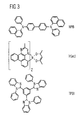
- FIG. 3 shows the structure of three organic compounds as they can be used for example in an OLED.
- the first structural formula shows NPB (N, N'-di (naphthyl-1-yl) -N-N'-diphenylbenzidine) which is useful, for example, as a hole transporting layer and matrix for emitting substances.
- the second structural formula shows Ir (ac) (iridium (III) bis (2-methyldibenzo [f, h] quinoxaline) (acetylacetonate)).
- the Ir complex can be used, for example, as a red phosphorescent dye in an OLED.
- the third structural formula shows TPBI (1,3,5-tris (1-phenyl-1H-benzimidazol-2-yl) benzene), the organic compound III.
- This compound can be used inter alia for the hole-blocking layer as well as for the electron-conducting layer 3.
- FIG. 4 schematically shows the energy levels of the individual layers of an embodiment of a device according to the invention, which is designed as an OLED.
- the LUMOs and HOMOs of the individual layers are given, as are the layer thicknesses of the individual layers.
- the transparent anode, which is made of ITO, is followed by a 30 nm thick layer of NPB.
- This first layer of NPB, which performs the function of hole transport, is followed by another layer in which NPB serves as the matrix material.
- This second layer of NPB is 7 nm thick and additionally has a proportion of 10 mol% iridium (III) bis (2-methyldibenzo [f, h] quinoxaline) (acetylacetonate) (Ir (ac)), whose structural formula in FIG. 3 is shown.
- Both the LUMO and the HOMO of the phosphorescent substance Ir (ac) are just below the corresponding energy levels of the matrix material NPD.
- the emitting layer is followed by a 10 nm thick layer of TPBI, the organic compound III. This layer has a hole blocking function.
- the energy levels of TPBI are each below the corresponding energy levels of the phosphorescent substance.
- the hole-blocking layer is followed by the electron-conducting layer (ETL).
- the electron-conducting layer in the embodiments according to the invention comprises a metal complex and an organic compound. This electron-conducting layer is obtainable by coevaporation of the metal complex with the organic compound.
- the electron-conducting layer in this embodiment performs the function of both the electron-injecting layer and the electron-transporting layer.
- the energy levels of the electron-conducting layer are above the corresponding energy levels of the hole-blocking layer.
- the electron-conducting layer is followed by a cathode made of Al. If voltage is now applied to the anode and the cathode, holes are induced by the anode and electrons are induced by the cathode into the hole-transporting or electron-transporting layer.
- the holes From there migrate the positive charge carriers, the "holes" and the Electrons in the NPB layer, which is doped with the phosphorescent material. Upon recombination of the holes and the electrons on the red emitter excitons are formed, which can excite the phosphorescent substance for emission.
- FIGS. 5 to 8 are measured curves of both inventive embodiments with metal complex in the ETL, as well as not inventive variants without metal complex in the ETL shown.
- the ETL is varied in each case.
- FIG. 5 shows three traces (21, 22, 23) in which the current density J is plotted against the voltage U.
- three OLED devices were fabricated from a 120 nm thick indium tin oxide electrode each followed by a 150 nm thick electron-conducting layer on which a 150 nm-thick Al electrode is arranged.
- the same organic compound namely the organic compound of structure V, was used for all three measurements for the electron-conducting layers 3 of the three components.
- a proportion of 10 mol% of W 2 (TBD-A) 4 is present in the organic compound V as a metal complex.
- the proportion of W 2 (TBD-A) 4 as a metal complex is only 1 mol%.
- the measurement curve 23 was carried out with the pure organic compound V, ie without a metal complex.
- the graph shows that even with a proportion of 1 mol% (curve 22) on the metal complex at higher voltages very good current densities can be achieved. Even at low voltage, the current densities, which are already achieved with 1 mol% of the metal complex (curve 22) are already significantly better than the current densities, which with the pure organic compound be achieved (trace 23).
- FIG. 5 hereby clearly shows the influence of the metal complex on the current density.
- the "free" electrons additionally provided by the metal complex can thus make a decisive contribution to the electron transport in the OLED component.
- FIG. 6 shows three measurement curves (31, 32, 33) in which the luminescence L is plotted against the voltage U.
- three components were manufactured whose structure corresponds to the structure, as in the comments on FIG. 4 describe is.
- the material for the electron-conducting layer was varied in each case.
- an electron-conducting layer of the organic compound II with a proportion of 10 mol% of W 2 (TBD-A) 4 was used.
- an electron-conducting layer of the organic compound I with a proportion of 10 mol% of W 2 (TBD-A) 4 was used.
- FIG. 7 shows three measurement curves (41, 42, 43) in which the radiation efficiency E is plotted against the luminescence L.
- the structure of the components that were used for these curves corresponds to the structure as in the comments on FIG. 4 describe is.
- the materials of the electron-conducting layer were varied from measurement curve to measurement curve.
- a device having an electron-conducting layer of the organic compound I in a proportion of 10 mol% of W 2 (TBD-A) 4 was used.
- TBD-A a device with an electron-conducting layer of the organic compound II with a proportion of 10 mol% of W 2
- the component of the measurement curve 43 additionally comprises a layer of LiF with a thickness of 0.7 nm between the electron-conducting layer and the Al electrode
- FIG. 7 can be clearly seen, the measurement curves 41 and 42, in which the electron-conducting layer in addition to the organic compound each additionally have a content of 10 mol% of the metal complex, a significantly improved efficiency over the trace 43 with the electron-conducting layer, the no metal complex includes. From the measured values in FIG. 7 Thus, it can be clearly seen that the efficiency of the component through the Metal complex which has been evaporated together with the organic compound, can be significantly increased.
- FIG. 8 shows three measurement curves (51, 52, 53) in which the luminescence L is plotted against the time t.
- the "lifetime" is defined as the 50% value of the originally set brightness, in this case 1000 cd / m 2 . If a component falls below the threshold value of 500 cd / m 2, then it is no longer usable, its "lifetime" is considered to have expired.
- components were used whose structure corresponds to the structure, as in the figure description to FIG. 4 describe is.
- the electron-conducting layer was varied in each case. In the measuring curve 51, a component was used in which the electron-conducting layer consists only of the organic compound I.
- the device additionally has between the electron-conducting layer and the Al electrode, a further layer of a thickness of 0.7 nm LiF.
- an electron-conducting layer of the organic compound I in a proportion of 10 mol% of W 2 (TBD-A) 4 was used.
- a device having an electron-conducting layer of the organic compound II with a proportion of 10 mol% of W 2 (TBD-A) 4 was used.
- FIG. 8 clearly shows that in the two measurement curves 52 and 53, in which the electron-conducting layer has a metal complex, significantly better lifetimes were achieved, as in the measurement curve 51, in which the electron-conducting layer has no metal complex. In this measurement could be achieved in the measurement curve 53 with the organic compound II again significantly better lifetimes (> 2500 h), as in the curve 52 with the organic compound I (235 h).
- the measured curves shown clearly show that the presence of the metal complex, which was vaporized together with the organic compound to form an electron-conducting layer, has a positive influence on the respectively measured electrical and optoelectronic parameters. It was possible in the corresponding organic electronic components, a higher current density, higher luminescence, better efficiency and longer life by the co-evaporation of the metal complex with the organic compound can be achieved.
- FIG. 9 shows a schematic side view of an embodiment of a device according to the invention, which is designed as an organic field effect transistor (OFET).
- OFET organic field effect transistor
- the first electrode 2 is arranged, which is formed as a gate electrode layer.
- the first electrode 2 is followed by an insulator layer 60, which may comprise, for example, a dielectric.
- the second electrode 4 is formed as source-drain contact layers and comprises an electron-conducting layer.
- a semiconductor 80 is arranged, which consists of a hole-conducting material.
- the organic field effect transistor further comprises a cover layer 70, which may serve for example for encapsulation.
Landscapes
- Chemical & Material Sciences (AREA)
- Physics & Mathematics (AREA)
- Engineering & Computer Science (AREA)
- Materials Engineering (AREA)
- Spectroscopy & Molecular Physics (AREA)
- High Energy & Nuclear Physics (AREA)
- Inorganic Chemistry (AREA)
- Optics & Photonics (AREA)
- Electroluminescent Light Sources (AREA)
- Photovoltaic Devices (AREA)
Applications Claiming Priority (3)
| Application Number | Priority Date | Filing Date | Title |
|---|---|---|---|
| DE102008049286 | 2008-09-26 | ||
| DE102008056391.9A DE102008056391B4 (de) | 2008-09-26 | 2008-11-07 | Organisches elektronisches Bauelement und Verfahren zu dessen Herstellung |
| PCT/DE2009/001359 WO2010034304A2 (de) | 2008-09-26 | 2009-09-25 | Organisches elektronisches bauelement und verfahren zu dessen herstellung |
Publications (2)
| Publication Number | Publication Date |
|---|---|
| EP2342772A2 EP2342772A2 (de) | 2011-07-13 |
| EP2342772B1 true EP2342772B1 (de) | 2015-12-02 |
Family
ID=41719954
Family Applications (1)
| Application Number | Title | Priority Date | Filing Date |
|---|---|---|---|
| EP09741205.0A Active EP2342772B1 (de) | 2008-09-26 | 2009-09-25 | Organisches elektronisches bauelement und verfahren zu dessen herstellung |
Country Status (7)
| Country | Link |
|---|---|
| US (1) | US8558223B2 (enExample) |
| EP (1) | EP2342772B1 (enExample) |
| JP (1) | JP5650114B2 (enExample) |
| KR (1) | KR101640621B1 (enExample) |
| CN (1) | CN102165622B (enExample) |
| DE (1) | DE102008056391B4 (enExample) |
| WO (1) | WO2010034304A2 (enExample) |
Families Citing this family (13)
| Publication number | Priority date | Publication date | Assignee | Title |
|---|---|---|---|---|
| CN102471269B (zh) | 2010-01-15 | 2016-02-03 | 出光兴产株式会社 | 含氮杂环衍生物及含有它的有机电致发光元件 |
| DE102012200180A1 (de) * | 2012-01-09 | 2013-07-11 | Osram Opto Semiconductors Gmbh | Verfahren zur Herstellung optoelektronischer organischer Bauteile, Vorrichtung hierfür und optoelektronisches organisches Bauteil |
| CN103390631A (zh) * | 2012-05-11 | 2013-11-13 | 四川优的科技有限公司 | 一种oled显示器结构 |
| JP6060530B2 (ja) * | 2012-06-12 | 2017-01-18 | ソニー株式会社 | 有機電界発光素子及び表示装置 |
| JP2015060020A (ja) * | 2013-09-18 | 2015-03-30 | ソニー株式会社 | 表示装置及び電子機器 |
| EP3284801A1 (en) | 2016-08-19 | 2018-02-21 | Julius-Maximilians-Universität Würzburg | Ligands, electrochromic metallo-polymers obtained therewith and their use |
| CN107698568A (zh) * | 2017-09-26 | 2018-02-16 | 长春海谱润斯科技有限公司 | 一种联嘧啶衍生物的热激活延迟荧光材料及其有机电致发光器件 |
| CN109994651B (zh) * | 2017-12-29 | 2020-12-25 | 昆山国显光电有限公司 | 一种有机电致发光器件及其制备方法 |
| US11380852B2 (en) * | 2018-12-12 | 2022-07-05 | The Regents Of The University Of California | N-type dopants for efficient solar cells |
| KR102381634B1 (ko) * | 2019-07-05 | 2022-04-01 | 주식회사 엘지화학 | 화합물 및 이를 포함하는 유기 발광 소자 |
| KR102291411B1 (ko) * | 2019-12-09 | 2021-08-23 | 엘티소재주식회사 | 헤테로고리 화합물 및 이를 포함하는 유기 발광 소자 |
| CN112194614B (zh) * | 2020-10-14 | 2022-04-26 | 新乡医学院 | 一种特异性识别Fe3+的三联吡啶荧光探针及其合成方法和应用 |
| CN115207228B (zh) * | 2021-04-08 | 2025-06-03 | 常州强力电子新材料股份有限公司 | 有机电致发光元件 |
Family Cites Families (48)
| Publication number | Priority date | Publication date | Assignee | Title |
|---|---|---|---|---|
| DE3022818C2 (de) * | 1980-06-19 | 1986-11-27 | Merck Patent Gmbh, 6100 Darmstadt | Flüssigkristall-Anzeigeelement |
| EP0191726A3 (de) * | 1985-01-17 | 1988-05-11 | Ciba-Geigy Ag | Polypyrrol-Polyimidzusammensetzungen |
| DE59106678D1 (de) * | 1990-12-21 | 1995-11-16 | Hoffmann La Roche | Optisch nichtlineare Polymerschichten. |
| JP3490727B2 (ja) * | 1991-11-28 | 2004-01-26 | 三洋電機株式会社 | 電界発光素子 |
| US5456988A (en) * | 1992-01-31 | 1995-10-10 | Sanyo Electric Co., Ltd. | Organic electroluminescent device having improved durability |
| US5529853A (en) * | 1993-03-17 | 1996-06-25 | Sanyo Electric Co., Ltd. | Organic electroluminescent element |
| US5466392A (en) * | 1993-06-02 | 1995-11-14 | Idemitsu Kosan Co., Ltd. | Organic electroluminescence device and compound having an aluminum complex structure |
| KR0139876B1 (ko) * | 1993-09-14 | 1998-08-17 | 사토 후미오 | 금속산화막의 형성방법 |
| US5504183A (en) * | 1994-09-12 | 1996-04-02 | Motorola | Organometallic fluorescent complex polymers for light emitting applications |
| US5837390A (en) * | 1995-05-10 | 1998-11-17 | Sony Corporation | Metal complex, method for producing the same and optical device |
| JPH08325564A (ja) * | 1995-06-05 | 1996-12-10 | Nec Corp | 有機薄膜el素子 |
| US5834894A (en) * | 1995-09-14 | 1998-11-10 | Casio Computer Co., Ltd. | Carrier injection type organic electro-luminescent device which emits light in response to an application of a voltage |
| KR0176076B1 (ko) * | 1996-08-28 | 1999-02-01 | 양승택 | 유기물/고분자 발광 소자의 구조 및 그 제조 방법 |
| JPH1160735A (ja) * | 1996-12-09 | 1999-03-05 | Toshiba Corp | ポリシランおよびパターン形成方法 |
| US5811833A (en) * | 1996-12-23 | 1998-09-22 | University Of So. Ca | Electron transporting and light emitting layers based on organic free radicals |
| JPH10183112A (ja) * | 1996-12-27 | 1998-07-14 | Sony Corp | 電界発光素子 |
| ATE437450T1 (de) * | 1997-10-09 | 2009-08-15 | Univ Princeton | Phosphoreszente organische lichtemittierende vorrichtung |
| GB9820805D0 (en) | 1998-09-25 | 1998-11-18 | Isis Innovation | Divalent lanthanide metal complexes |
| GB9826405D0 (en) * | 1998-12-02 | 1999-01-27 | South Bank Univ Entpr Ltd | Method for forming films or layers |
| JP4505067B2 (ja) * | 1998-12-16 | 2010-07-14 | 淳二 城戸 | 有機エレクトロルミネッセント素子 |
| GB9917356D0 (en) * | 1999-07-24 | 1999-09-22 | Univ Cambridge Tech | Aromatic monomers and polymers for optoelectronic devices |
| JP3982164B2 (ja) * | 2000-09-26 | 2007-09-26 | 三菱化学株式会社 | 有機電界発光素子及びその製造方法 |
| US6764776B2 (en) | 2000-11-30 | 2004-07-20 | Semiconductor Energy Laboratory Co., Ltd. | Light emitting device |
| US7414359B2 (en) * | 2002-08-12 | 2008-08-19 | Colorado State University Research Foundation | Low work function metal complexes and uses thereof |
| JP2004265740A (ja) * | 2003-02-28 | 2004-09-24 | Tdk Corp | El機能膜及びel素子 |
| US8513375B2 (en) * | 2003-05-05 | 2013-08-20 | Designer Molecules, Inc. | Imide-linked maleimide and polymaleimide compounds |
| EP1491568A1 (en) * | 2003-06-23 | 2004-12-29 | Covion Organic Semiconductors GmbH | Semiconductive Polymers |
| US20060163562A1 (en) * | 2003-07-07 | 2006-07-27 | Koninklijke Philips Electronics N.V. | Multifluorinated conductor material for leds for improving the light outcoupling |
| JP2005056757A (ja) | 2003-08-06 | 2005-03-03 | Seiko Epson Corp | 有機エレクトロルミネッセンス装置の製造方法、有機エレクトロルミネッセンス装置、電子機器 |
| DE10337346A1 (de) * | 2003-08-12 | 2005-03-31 | Covion Organic Semiconductors Gmbh | Konjugierte Polymere enthaltend Dihydrophenanthren-Einheiten und deren Verwendung |
| DE10339772B4 (de) * | 2003-08-27 | 2006-07-13 | Novaled Gmbh | Licht emittierendes Bauelement und Verfahren zu seiner Herstellung |
| US20050048422A1 (en) * | 2003-09-01 | 2005-03-03 | Hajime Nakagawa | Packaged member of photothermographic material and image forming method for photothermographic material |
| DE102004010954A1 (de) * | 2004-03-03 | 2005-10-06 | Novaled Gmbh | Verwendung eines Metallkomplexes als n-Dotand für ein organisches halbleitendes Matrixmaterial, organisches Halbleitermaterial und elektronisches Bauteil |
| US7622200B2 (en) * | 2004-05-21 | 2009-11-24 | Semiconductor Energy Laboratory Co., Ltd. | Light emitting element |
| US20060036114A1 (en) * | 2004-08-13 | 2006-02-16 | Suning Wang | Organoboron luminescent compounds and methods of making and using same |
| US20060115536A1 (en) * | 2004-11-12 | 2006-06-01 | Board Of Regents, The University Of Texas System | Glycerin based synthesis of silver nanoparticles and nanowires |
| US7485471B1 (en) * | 2004-12-17 | 2009-02-03 | Intel Corporation | Detection of enhanced multiplex signals by surface enhanced Raman spectroscopy |
| JP5159042B2 (ja) * | 2005-02-08 | 2013-03-06 | 株式会社半導体エネルギー研究所 | 発光素子、発光装置及び電子機器 |
| WO2006085538A2 (en) * | 2005-02-08 | 2006-08-17 | Semiconductor Energy Laboratory Co., Ltd. | Light-emitting element, light-emitting device, and electronic appliance |
| JP5040080B2 (ja) * | 2005-07-20 | 2012-10-03 | Jnc株式会社 | 有機電界発光素子 |
| JP4959961B2 (ja) * | 2005-07-29 | 2012-06-27 | 株式会社ジャパンディスプレイセントラル | 有機el素子の製造方法 |
| JP5208391B2 (ja) * | 2005-09-09 | 2013-06-12 | 住友化学株式会社 | 金属錯体、発光材料及び発光素子 |
| EP1786050B1 (de) | 2005-11-10 | 2010-06-23 | Novaled AG | Dotiertes organisches Halbleitermaterial |
| WO2008006373A1 (en) * | 2006-07-12 | 2008-01-17 | Merck Patent Gmbh | Solid-phase detection of terminal monosaccharides cleaved from glycosylated substrates |
| US8328375B2 (en) * | 2006-09-29 | 2012-12-11 | Osram Opto Semiconductors Gmbh | Organic lighting device and lighting equipment |
| JP4478166B2 (ja) * | 2006-11-09 | 2010-06-09 | 三星モバイルディスプレイ株式會社 | 有機金属錯体を含む有機膜を備えた有機発光素子 |
| WO2009143604A1 (en) * | 2008-05-30 | 2009-12-03 | University Of Alberta | Molecular signature for fibrosis and atrophy |
| EP2330908A4 (en) * | 2008-08-15 | 2011-11-23 | Univ Georgetown | FLUORESCENT CDK INHIBITORS FOR CANCER TREATMENT |
-
2008
- 2008-11-07 DE DE102008056391.9A patent/DE102008056391B4/de active Active
-
2009
- 2009-09-25 JP JP2011528186A patent/JP5650114B2/ja active Active
- 2009-09-25 EP EP09741205.0A patent/EP2342772B1/de active Active
- 2009-09-25 WO PCT/DE2009/001359 patent/WO2010034304A2/de not_active Ceased
- 2009-09-25 CN CN200980138172.2A patent/CN102165622B/zh active Active
- 2009-09-25 KR KR1020117009229A patent/KR101640621B1/ko active Active
- 2009-09-25 US US13/121,090 patent/US8558223B2/en active Active
Also Published As
| Publication number | Publication date |
|---|---|
| CN102165622B (zh) | 2014-09-17 |
| CN102165622A (zh) | 2011-08-24 |
| WO2010034304A3 (de) | 2010-06-03 |
| DE102008056391B4 (de) | 2021-04-01 |
| KR20110084406A (ko) | 2011-07-22 |
| KR101640621B1 (ko) | 2016-07-18 |
| WO2010034304A2 (de) | 2010-04-01 |
| JP2012503867A (ja) | 2012-02-09 |
| JP5650114B2 (ja) | 2015-01-07 |
| US20110309340A1 (en) | 2011-12-22 |
| US8558223B2 (en) | 2013-10-15 |
| DE102008056391A1 (de) | 2010-04-01 |
| EP2342772A2 (de) | 2011-07-13 |
Similar Documents
| Publication | Publication Date | Title |
|---|---|---|
| EP2342772B1 (de) | Organisches elektronisches bauelement und verfahren zu dessen herstellung | |
| DE112007000135B4 (de) | Elektrolumineszente Lichtemissionseinrichtung mit einer Anordnung organischer Schichten und Verfahren zum Herstellen | |
| DE69027760T2 (de) | Organisches elektrolumineszentes element | |
| DE69531509T2 (de) | Organisch/anorganische legierungen zur verbesserung organischer elektroluminiszierender vorrichtungen | |
| EP1508176B1 (de) | Phosphoreszentes lichtemittierendes bauelement mit organischen schichten | |
| DE102013017361B4 (de) | Organisches Licht emittierendes Bauelement und Verfahren zur Herstellung eines organischen Licht ermittierenden Bauelements | |
| DE10215210B4 (de) | Transparentes, thermisch stabiles lichtemittierendes Bauelement mit organischen Schichten | |
| EP1687859B1 (de) | Organisches elektrolumineszenzelement | |
| EP1861886B1 (de) | Organisches photoaktives bauelement | |
| EP2483945B1 (de) | Organische elektronische vorrichtung und verfahren zu deren herstellung | |
| EP2229699B1 (de) | Dithiolenübergangsmetallkomplexe und elektronische oder optoelektronische bauelemente | |
| WO2006092135A1 (de) | Photoaktives bauelement mit organischen schichten | |
| WO2010075836A2 (de) | Heterocyclische verbindungen und deren verwendung in elektronischen und optoelektronischen bauelementen | |
| WO2007054345A1 (de) | Dotiertes organisches halbleitermaterial | |
| DE102013107113B4 (de) | Organisches Licht emittierendes Bauelement und Verfahren zur Herstellung eines organischen Licht emittierenden Bauelements | |
| WO2011134458A1 (de) | Organisches halbleitendes material und elektronisches bauelement | |
| WO2008061518A2 (de) | Dithiolenübergangsmetallkomplexe und selen-analoge verbindungen, deren verwendung als dotand, organisches halbleitendes material enthaltend die komplexe, sowie elektronische oder optoelektronische bauelemente enthaltend einen komplex | |
| WO2012136422A1 (de) | Optoelektronisches bauelement und verwendung eines kupferkomplexes als dotierstoff zum dotieren einer schicht | |
| EP2140512B1 (de) | Elektrisches organisches bauelement und verfahren zu seiner herstellung | |
| DE102013106949A1 (de) | Optoelektronisches Bauelement, organische funktionelle Schicht und Verfahren zur Herstellung eines optoelektronischen Bauelements | |
| WO2017178473A1 (de) | Organisches elektronisches bauteil mit ladungsträger-generationsschicht | |
| DE102013103156B4 (de) | Strahlungsemittierende organisch-elektronische Vorrichtung und Verfahren zur Herstellung einer strahlungsemittierenden organisch-elektronischen Vorrichtung | |
| WO2010133205A1 (de) | Organische solarzelle oder photodetektor mit verbesserter absorption | |
| DE102007059887B4 (de) | Lichtemittierendes organisches Bauelement und Verfahren zu dessen Herstellung | |
| DE102008058230B4 (de) | Chinoxalinverbindung, organische Leuchtdiode, organischer Dünnfilmtransistor und Solarzelle |
Legal Events
| Date | Code | Title | Description |
|---|---|---|---|
| PUAI | Public reference made under article 153(3) epc to a published international application that has entered the european phase |
Free format text: ORIGINAL CODE: 0009012 |
|
| 17P | Request for examination filed |
Effective date: 20110426 |
|
| AK | Designated contracting states |
Kind code of ref document: A2 Designated state(s): AT BE BG CH CY CZ DE DK EE ES FI FR GB GR HR HU IE IS IT LI LT LU LV MC MK MT NL NO PL PT RO SE SI SK SM TR |
|
| AX | Request for extension of the european patent |
Extension state: AL BA RS |
|
| DAX | Request for extension of the european patent (deleted) | ||
| 17Q | First examination report despatched |
Effective date: 20120824 |
|
| GRAP | Despatch of communication of intention to grant a patent |
Free format text: ORIGINAL CODE: EPIDOSNIGR1 |
|
| INTG | Intention to grant announced |
Effective date: 20150728 |
|
| RAP1 | Party data changed (applicant data changed or rights of an application transferred) |
Owner name: OSRAM OLED GMBH |
|
| GRAS | Grant fee paid |
Free format text: ORIGINAL CODE: EPIDOSNIGR3 |
|
| GRAA | (expected) grant |
Free format text: ORIGINAL CODE: 0009210 |
|
| AK | Designated contracting states |
Kind code of ref document: B1 Designated state(s): AT BE BG CH CY CZ DE DK EE ES FI FR GB GR HR HU IE IS IT LI LT LU LV MC MK MT NL NO PL PT RO SE SI SK SM TR |
|
| REG | Reference to a national code |
Ref country code: GB Ref legal event code: FG4D Free format text: NOT ENGLISH |
|
| REG | Reference to a national code |
Ref country code: AT Ref legal event code: REF Ref document number: 763974 Country of ref document: AT Kind code of ref document: T Effective date: 20151215 Ref country code: CH Ref legal event code: EP |
|
| REG | Reference to a national code |
Ref country code: IE Ref legal event code: FG4D Free format text: LANGUAGE OF EP DOCUMENT: GERMAN |
|
| REG | Reference to a national code |
Ref country code: DE Ref legal event code: R096 Ref document number: 502009011893 Country of ref document: DE |
|
| REG | Reference to a national code |
Ref country code: NL Ref legal event code: MP Effective date: 20160302 |
|
| REG | Reference to a national code |
Ref country code: LT Ref legal event code: MG4D |
|
| PG25 | Lapsed in a contracting state [announced via postgrant information from national office to epo] |
Ref country code: HR Free format text: LAPSE BECAUSE OF FAILURE TO SUBMIT A TRANSLATION OF THE DESCRIPTION OR TO PAY THE FEE WITHIN THE PRESCRIBED TIME-LIMIT Effective date: 20151202 Ref country code: NO Free format text: LAPSE BECAUSE OF FAILURE TO SUBMIT A TRANSLATION OF THE DESCRIPTION OR TO PAY THE FEE WITHIN THE PRESCRIBED TIME-LIMIT Effective date: 20160302 Ref country code: LT Free format text: LAPSE BECAUSE OF FAILURE TO SUBMIT A TRANSLATION OF THE DESCRIPTION OR TO PAY THE FEE WITHIN THE PRESCRIBED TIME-LIMIT Effective date: 20151202 Ref country code: ES Free format text: LAPSE BECAUSE OF FAILURE TO SUBMIT A TRANSLATION OF THE DESCRIPTION OR TO PAY THE FEE WITHIN THE PRESCRIBED TIME-LIMIT Effective date: 20151202 |
|
| PG25 | Lapsed in a contracting state [announced via postgrant information from national office to epo] |
Ref country code: SE Free format text: LAPSE BECAUSE OF FAILURE TO SUBMIT A TRANSLATION OF THE DESCRIPTION OR TO PAY THE FEE WITHIN THE PRESCRIBED TIME-LIMIT Effective date: 20151202 Ref country code: PL Free format text: LAPSE BECAUSE OF FAILURE TO SUBMIT A TRANSLATION OF THE DESCRIPTION OR TO PAY THE FEE WITHIN THE PRESCRIBED TIME-LIMIT Effective date: 20151202 Ref country code: LV Free format text: LAPSE BECAUSE OF FAILURE TO SUBMIT A TRANSLATION OF THE DESCRIPTION OR TO PAY THE FEE WITHIN THE PRESCRIBED TIME-LIMIT Effective date: 20151202 Ref country code: GR Free format text: LAPSE BECAUSE OF FAILURE TO SUBMIT A TRANSLATION OF THE DESCRIPTION OR TO PAY THE FEE WITHIN THE PRESCRIBED TIME-LIMIT Effective date: 20160303 Ref country code: NL Free format text: LAPSE BECAUSE OF FAILURE TO SUBMIT A TRANSLATION OF THE DESCRIPTION OR TO PAY THE FEE WITHIN THE PRESCRIBED TIME-LIMIT Effective date: 20151202 Ref country code: FI Free format text: LAPSE BECAUSE OF FAILURE TO SUBMIT A TRANSLATION OF THE DESCRIPTION OR TO PAY THE FEE WITHIN THE PRESCRIBED TIME-LIMIT Effective date: 20151202 |
|
| PG25 | Lapsed in a contracting state [announced via postgrant information from national office to epo] |
Ref country code: IS Free format text: LAPSE BECAUSE OF FAILURE TO SUBMIT A TRANSLATION OF THE DESCRIPTION OR TO PAY THE FEE WITHIN THE PRESCRIBED TIME-LIMIT Effective date: 20151202 |
|
| PG25 | Lapsed in a contracting state [announced via postgrant information from national office to epo] |
Ref country code: CZ Free format text: LAPSE BECAUSE OF FAILURE TO SUBMIT A TRANSLATION OF THE DESCRIPTION OR TO PAY THE FEE WITHIN THE PRESCRIBED TIME-LIMIT Effective date: 20151202 Ref country code: IT Free format text: LAPSE BECAUSE OF FAILURE TO SUBMIT A TRANSLATION OF THE DESCRIPTION OR TO PAY THE FEE WITHIN THE PRESCRIBED TIME-LIMIT Effective date: 20151202 |
|
| PG25 | Lapsed in a contracting state [announced via postgrant information from national office to epo] |
Ref country code: RO Free format text: LAPSE BECAUSE OF FAILURE TO SUBMIT A TRANSLATION OF THE DESCRIPTION OR TO PAY THE FEE WITHIN THE PRESCRIBED TIME-LIMIT Effective date: 20151202 Ref country code: SK Free format text: LAPSE BECAUSE OF FAILURE TO SUBMIT A TRANSLATION OF THE DESCRIPTION OR TO PAY THE FEE WITHIN THE PRESCRIBED TIME-LIMIT Effective date: 20151202 Ref country code: EE Free format text: LAPSE BECAUSE OF FAILURE TO SUBMIT A TRANSLATION OF THE DESCRIPTION OR TO PAY THE FEE WITHIN THE PRESCRIBED TIME-LIMIT Effective date: 20151202 Ref country code: IS Free format text: LAPSE BECAUSE OF FAILURE TO SUBMIT A TRANSLATION OF THE DESCRIPTION OR TO PAY THE FEE WITHIN THE PRESCRIBED TIME-LIMIT Effective date: 20160402 Ref country code: SM Free format text: LAPSE BECAUSE OF FAILURE TO SUBMIT A TRANSLATION OF THE DESCRIPTION OR TO PAY THE FEE WITHIN THE PRESCRIBED TIME-LIMIT Effective date: 20151202 Ref country code: PT Free format text: LAPSE BECAUSE OF FAILURE TO SUBMIT A TRANSLATION OF THE DESCRIPTION OR TO PAY THE FEE WITHIN THE PRESCRIBED TIME-LIMIT Effective date: 20160404 |
|
| REG | Reference to a national code |
Ref country code: DE Ref legal event code: R097 Ref document number: 502009011893 Country of ref document: DE |
|
| PLBE | No opposition filed within time limit |
Free format text: ORIGINAL CODE: 0009261 |
|
| STAA | Information on the status of an ep patent application or granted ep patent |
Free format text: STATUS: NO OPPOSITION FILED WITHIN TIME LIMIT |
|
| PG25 | Lapsed in a contracting state [announced via postgrant information from national office to epo] |
Ref country code: DK Free format text: LAPSE BECAUSE OF FAILURE TO SUBMIT A TRANSLATION OF THE DESCRIPTION OR TO PAY THE FEE WITHIN THE PRESCRIBED TIME-LIMIT Effective date: 20151202 |
|
| 26N | No opposition filed |
Effective date: 20160905 |
|
| PG25 | Lapsed in a contracting state [announced via postgrant information from national office to epo] |
Ref country code: SI Free format text: LAPSE BECAUSE OF FAILURE TO SUBMIT A TRANSLATION OF THE DESCRIPTION OR TO PAY THE FEE WITHIN THE PRESCRIBED TIME-LIMIT Effective date: 20151202 |
|
| PG25 | Lapsed in a contracting state [announced via postgrant information from national office to epo] |
Ref country code: BE Free format text: LAPSE BECAUSE OF NON-PAYMENT OF DUE FEES Effective date: 20160930 |
|
| PG25 | Lapsed in a contracting state [announced via postgrant information from national office to epo] |
Ref country code: MC Free format text: LAPSE BECAUSE OF FAILURE TO SUBMIT A TRANSLATION OF THE DESCRIPTION OR TO PAY THE FEE WITHIN THE PRESCRIBED TIME-LIMIT Effective date: 20151202 |
|
| REG | Reference to a national code |
Ref country code: CH Ref legal event code: PL |
|
| GBPC | Gb: european patent ceased through non-payment of renewal fee |
Effective date: 20160925 |
|
| REG | Reference to a national code |
Ref country code: IE Ref legal event code: MM4A |
|
| REG | Reference to a national code |
Ref country code: FR Ref legal event code: ST Effective date: 20170531 |
|
| PG25 | Lapsed in a contracting state [announced via postgrant information from national office to epo] |
Ref country code: FR Free format text: LAPSE BECAUSE OF NON-PAYMENT OF DUE FEES Effective date: 20160930 Ref country code: LI Free format text: LAPSE BECAUSE OF NON-PAYMENT OF DUE FEES Effective date: 20160930 Ref country code: GB Free format text: LAPSE BECAUSE OF NON-PAYMENT OF DUE FEES Effective date: 20160925 Ref country code: CH Free format text: LAPSE BECAUSE OF NON-PAYMENT OF DUE FEES Effective date: 20160930 Ref country code: IE Free format text: LAPSE BECAUSE OF NON-PAYMENT OF DUE FEES Effective date: 20160925 |
|
| PG25 | Lapsed in a contracting state [announced via postgrant information from national office to epo] |
Ref country code: LU Free format text: LAPSE BECAUSE OF NON-PAYMENT OF DUE FEES Effective date: 20160925 |
|
| REG | Reference to a national code |
Ref country code: AT Ref legal event code: MM01 Ref document number: 763974 Country of ref document: AT Kind code of ref document: T Effective date: 20160925 |
|
| REG | Reference to a national code |
Ref country code: BE Ref legal event code: MM Effective date: 20160930 |
|
| PG25 | Lapsed in a contracting state [announced via postgrant information from national office to epo] |
Ref country code: AT Free format text: LAPSE BECAUSE OF NON-PAYMENT OF DUE FEES Effective date: 20160925 |
|
| PG25 | Lapsed in a contracting state [announced via postgrant information from national office to epo] |
Ref country code: CY Free format text: LAPSE BECAUSE OF FAILURE TO SUBMIT A TRANSLATION OF THE DESCRIPTION OR TO PAY THE FEE WITHIN THE PRESCRIBED TIME-LIMIT Effective date: 20151202 Ref country code: HU Free format text: LAPSE BECAUSE OF FAILURE TO SUBMIT A TRANSLATION OF THE DESCRIPTION OR TO PAY THE FEE WITHIN THE PRESCRIBED TIME-LIMIT; INVALID AB INITIO Effective date: 20090925 |
|
| PG25 | Lapsed in a contracting state [announced via postgrant information from national office to epo] |
Ref country code: MT Free format text: LAPSE BECAUSE OF FAILURE TO SUBMIT A TRANSLATION OF THE DESCRIPTION OR TO PAY THE FEE WITHIN THE PRESCRIBED TIME-LIMIT Effective date: 20151202 Ref country code: TR Free format text: LAPSE BECAUSE OF FAILURE TO SUBMIT A TRANSLATION OF THE DESCRIPTION OR TO PAY THE FEE WITHIN THE PRESCRIBED TIME-LIMIT Effective date: 20151202 Ref country code: MK Free format text: LAPSE BECAUSE OF FAILURE TO SUBMIT A TRANSLATION OF THE DESCRIPTION OR TO PAY THE FEE WITHIN THE PRESCRIBED TIME-LIMIT Effective date: 20151202 |
|
| PG25 | Lapsed in a contracting state [announced via postgrant information from national office to epo] |
Ref country code: BG Free format text: LAPSE BECAUSE OF FAILURE TO SUBMIT A TRANSLATION OF THE DESCRIPTION OR TO PAY THE FEE WITHIN THE PRESCRIBED TIME-LIMIT Effective date: 20151202 |
|
| REG | Reference to a national code |
Ref country code: DE Ref legal event code: R079 Ref document number: 502009011893 Country of ref document: DE Free format text: PREVIOUS MAIN CLASS: H01L0051540000 Ipc: H10K0085000000 |
|
| REG | Reference to a national code |
Ref country code: DE Ref legal event code: R081 Ref document number: 502009011893 Country of ref document: DE Owner name: PICTIVA DISPLAYS INTERNATIONAL LTD., IE Free format text: FORMER OWNER: OSRAM OLED GMBH, 93049 REGENSBURG, DE |
|
| REG | Reference to a national code |
Ref country code: DE Ref legal event code: R082 Ref document number: 502009011893 Country of ref document: DE Representative=s name: PETERREINS SCHLEY PATENT- UND RECHTSANWAELTE P, DE |
|
| PGFP | Annual fee paid to national office [announced via postgrant information from national office to epo] |
Ref country code: DE Payment date: 20250924 Year of fee payment: 17 |