EP2342772B1 - Organic electronic component and method for the production thereof - Google Patents
Organic electronic component and method for the production thereof Download PDFInfo
- Publication number
- EP2342772B1 EP2342772B1 EP09741205.0A EP09741205A EP2342772B1 EP 2342772 B1 EP2342772 B1 EP 2342772B1 EP 09741205 A EP09741205 A EP 09741205A EP 2342772 B1 EP2342772 B1 EP 2342772B1
- Authority
- EP
- European Patent Office
- Prior art keywords
- electron
- organic
- organic compound
- layer
- metal complex
- Prior art date
- Legal status (The legal status is an assumption and is not a legal conclusion. Google has not performed a legal analysis and makes no representation as to the accuracy of the status listed.)
- Active
Links
- 238000000034 method Methods 0.000 title claims description 23
- 238000004519 manufacturing process Methods 0.000 title description 4
- 150000002894 organic compounds Chemical class 0.000 claims description 113
- 150000004696 coordination complex Chemical class 0.000 claims description 76
- 229910052751 metal Inorganic materials 0.000 claims description 48
- 239000002184 metal Substances 0.000 claims description 48
- 239000000758 substrate Substances 0.000 claims description 19
- 238000001704 evaporation Methods 0.000 claims description 13
- 230000008569 process Effects 0.000 claims description 11
- 238000000151 deposition Methods 0.000 claims description 8
- 150000002390 heteroarenes Chemical class 0.000 claims description 7
- 229910052804 chromium Inorganic materials 0.000 claims description 5
- 238000010549 co-Evaporation Methods 0.000 claims description 5
- 229910052750 molybdenum Inorganic materials 0.000 claims description 5
- 229910052721 tungsten Inorganic materials 0.000 claims description 5
- 238000004132 cross linking Methods 0.000 claims description 3
- 150000001491 aromatic compounds Chemical class 0.000 claims 1
- 238000005259 measurement Methods 0.000 description 39
- 150000001875 compounds Chemical class 0.000 description 27
- 125000004429 atom Chemical group 0.000 description 26
- 239000003446 ligand Substances 0.000 description 17
- 229920000742 Cotton Polymers 0.000 description 13
- 125000003118 aryl group Chemical group 0.000 description 13
- 125000001072 heteroaryl group Chemical group 0.000 description 13
- 230000015572 biosynthetic process Effects 0.000 description 12
- 238000004020 luminiscence type Methods 0.000 description 12
- 230000008020 evaporation Effects 0.000 description 10
- 230000005855 radiation Effects 0.000 description 9
- 125000005842 heteroatom Chemical group 0.000 description 8
- 239000000126 substance Substances 0.000 description 8
- 238000012546 transfer Methods 0.000 description 8
- 239000002800 charge carrier Substances 0.000 description 7
- 238000004770 highest occupied molecular orbital Methods 0.000 description 6
- 238000004768 lowest unoccupied molecular orbital Methods 0.000 description 6
- 125000001997 phenyl group Chemical group [H]C1=C([H])C([H])=C(*)C([H])=C1[H] 0.000 description 6
- 230000005669 field effect Effects 0.000 description 5
- 239000007789 gas Substances 0.000 description 5
- 230000005525 hole transport Effects 0.000 description 5
- 125000002496 methyl group Chemical group [H]C([H])([H])* 0.000 description 5
- 229910052757 nitrogen Inorganic materials 0.000 description 5
- 239000012071 phase Substances 0.000 description 5
- 238000005215 recombination Methods 0.000 description 5
- 230000006798 recombination Effects 0.000 description 5
- 239000010948 rhodium Substances 0.000 description 5
- GEQBRULPNIVQPP-UHFFFAOYSA-N 2-[3,5-bis(1-phenylbenzimidazol-2-yl)phenyl]-1-phenylbenzimidazole Chemical compound C1=CC=CC=C1N1C2=CC=CC=C2N=C1C1=CC(C=2N(C3=CC=CC=C3N=2)C=2C=CC=CC=2)=CC(C=2N(C3=CC=CC=C3N=2)C=2C=CC=CC=2)=C1 GEQBRULPNIVQPP-UHFFFAOYSA-N 0.000 description 4
- 125000004105 2-pyridyl group Chemical group N1=C([*])C([H])=C([H])C([H])=C1[H] 0.000 description 4
- 125000003349 3-pyridyl group Chemical group N1=C([H])C([*])=C([H])C([H])=C1[H] 0.000 description 4
- 125000000339 4-pyridyl group Chemical group N1=C([H])C([H])=C([*])C([H])=C1[H] 0.000 description 4
- 241001295925 Gegenes Species 0.000 description 4
- 230000008021 deposition Effects 0.000 description 4
- 238000002347 injection Methods 0.000 description 4
- 239000007924 injection Substances 0.000 description 4
- 239000011159 matrix material Substances 0.000 description 4
- 125000002524 organometallic group Chemical group 0.000 description 4
- 229910052760 oxygen Inorganic materials 0.000 description 4
- 229910052703 rhodium Inorganic materials 0.000 description 4
- MHOVAHRLVXNVSD-UHFFFAOYSA-N rhodium atom Chemical compound [Rh] MHOVAHRLVXNVSD-UHFFFAOYSA-N 0.000 description 4
- 229910052717 sulfur Inorganic materials 0.000 description 4
- KAKZBPTYRLMSJV-UHFFFAOYSA-N Butadiene Chemical compound C=CC=C KAKZBPTYRLMSJV-UHFFFAOYSA-N 0.000 description 3
- JUJWROOIHBZHMG-UHFFFAOYSA-N Pyridine Chemical compound C1=CC=NC=C1 JUJWROOIHBZHMG-UHFFFAOYSA-N 0.000 description 3
- 238000010521 absorption reaction Methods 0.000 description 3
- 230000008901 benefit Effects 0.000 description 3
- 230000021615 conjugation Effects 0.000 description 3
- AMGQUBHHOARCQH-UHFFFAOYSA-N indium;oxotin Chemical compound [In].[Sn]=O AMGQUBHHOARCQH-UHFFFAOYSA-N 0.000 description 3
- 239000000463 material Substances 0.000 description 3
- IJGRMHOSHXDMSA-UHFFFAOYSA-N nitrogen Substances N#N IJGRMHOSHXDMSA-UHFFFAOYSA-N 0.000 description 3
- POILWHVDKZOXJZ-ARJAWSKDSA-M (z)-4-oxopent-2-en-2-olate Chemical compound C\C([O-])=C\C(C)=O POILWHVDKZOXJZ-ARJAWSKDSA-M 0.000 description 2
- NFNALQOLQWJCNE-UHFFFAOYSA-N [Ir+3].C1=CC=C2C3=NC(C)=CN=C3C3=CC=CC=C3C2=C1.C1=CC=C2C3=NC(C)=CN=C3C3=CC=CC=C3C2=C1 Chemical compound [Ir+3].C1=CC=C2C3=NC(C)=CN=C3C3=CC=CC=C3C2=C1.C1=CC=C2C3=NC(C)=CN=C3C3=CC=CC=C3C2=C1 NFNALQOLQWJCNE-UHFFFAOYSA-N 0.000 description 2
- 239000000919 ceramic Substances 0.000 description 2
- 238000002425 crystallisation Methods 0.000 description 2
- 230000008025 crystallization Effects 0.000 description 2
- 239000011521 glass Substances 0.000 description 2
- 239000012212 insulator Substances 0.000 description 2
- 230000003993 interaction Effects 0.000 description 2
- 229910052741 iridium Inorganic materials 0.000 description 2
- 230000005693 optoelectronics Effects 0.000 description 2
- 238000013021 overheating Methods 0.000 description 2
- 239000010453 quartz Substances 0.000 description 2
- 230000027756 respiratory electron transport chain Effects 0.000 description 2
- 239000004065 semiconductor Substances 0.000 description 2
- VYPSYNLAJGMNEJ-UHFFFAOYSA-N silicon dioxide Inorganic materials O=[Si]=O VYPSYNLAJGMNEJ-UHFFFAOYSA-N 0.000 description 2
- 238000009834 vaporization Methods 0.000 description 2
- 230000008016 vaporization Effects 0.000 description 2
- WSNMPAVSZJSIMT-UHFFFAOYSA-N COc1c(C)c2COC(=O)c2c(O)c1CC(O)C1(C)CCC(=O)O1 Chemical compound COc1c(C)c2COC(=O)c2c(O)c1CC(O)C1(C)CCC(=O)O1 WSNMPAVSZJSIMT-UHFFFAOYSA-N 0.000 description 1
- VGGSQFUCUMXWEO-UHFFFAOYSA-N Ethene Chemical compound C=C VGGSQFUCUMXWEO-UHFFFAOYSA-N 0.000 description 1
- 239000005977 Ethylene Substances 0.000 description 1
- UFHFLCQGNIYNRP-UHFFFAOYSA-N Hydrogen Chemical compound [H][H] UFHFLCQGNIYNRP-UHFFFAOYSA-N 0.000 description 1
- 239000000654 additive Substances 0.000 description 1
- 229910052782 aluminium Inorganic materials 0.000 description 1
- XAGFODPZIPBFFR-UHFFFAOYSA-N aluminium Chemical compound [Al] XAGFODPZIPBFFR-UHFFFAOYSA-N 0.000 description 1
- 150000001450 anions Chemical class 0.000 description 1
- 230000009286 beneficial effect Effects 0.000 description 1
- 230000000903 blocking effect Effects 0.000 description 1
- 125000004432 carbon atom Chemical group C* 0.000 description 1
- CREMABGTGYGIQB-UHFFFAOYSA-N carbon carbon Chemical compound C.C CREMABGTGYGIQB-UHFFFAOYSA-N 0.000 description 1
- 239000011203 carbon fibre reinforced carbon Substances 0.000 description 1
- 230000008859 change Effects 0.000 description 1
- 238000006243 chemical reaction Methods 0.000 description 1
- 239000004020 conductor Substances 0.000 description 1
- 125000004122 cyclic group Chemical group 0.000 description 1
- UURSXESKOOOTOV-UHFFFAOYSA-N dec-5-ene Chemical compound CCCCC=CCCCC UURSXESKOOOTOV-UHFFFAOYSA-N 0.000 description 1
- 238000012217 deletion Methods 0.000 description 1
- 230000037430 deletion Effects 0.000 description 1
- 238000005538 encapsulation Methods 0.000 description 1
- 230000004907 flux Effects 0.000 description 1
- -1 for example Chemical class 0.000 description 1
- 239000007792 gaseous phase Substances 0.000 description 1
- 230000003760 hair shine Effects 0.000 description 1
- 229910052739 hydrogen Inorganic materials 0.000 description 1
- 239000001257 hydrogen Substances 0.000 description 1
- 125000004433 nitrogen atom Chemical group N* 0.000 description 1
- QJGQUHMNIGDVPM-UHFFFAOYSA-N nitrogen group Chemical group [N] QJGQUHMNIGDVPM-UHFFFAOYSA-N 0.000 description 1
- 150000003961 organosilicon compounds Chemical class 0.000 description 1
- 230000003647 oxidation Effects 0.000 description 1
- 238000007254 oxidation reaction Methods 0.000 description 1
- 230000008092 positive effect Effects 0.000 description 1
- WGDRAVMHLDKGGA-UHFFFAOYSA-N prop-2-en-1-imine Chemical compound [CH2]C=C[NH] WGDRAVMHLDKGGA-UHFFFAOYSA-N 0.000 description 1
- UMJSCPRVCHMLSP-UHFFFAOYSA-N pyridine Natural products COC1=CC=CN=C1 UMJSCPRVCHMLSP-UHFFFAOYSA-N 0.000 description 1
- 125000004076 pyridyl group Chemical group 0.000 description 1
- 125000000714 pyrimidinyl group Chemical group 0.000 description 1
- 238000010791 quenching Methods 0.000 description 1
- 230000000171 quenching effect Effects 0.000 description 1
- 230000000717 retained effect Effects 0.000 description 1
- 238000012552 review Methods 0.000 description 1
- 229920006395 saturated elastomer Polymers 0.000 description 1
- 238000000926 separation method Methods 0.000 description 1
- 239000007790 solid phase Substances 0.000 description 1
- 125000001424 substituent group Chemical group 0.000 description 1
Images


Classifications
-
- H—ELECTRICITY
- H10—SEMICONDUCTOR DEVICES; ELECTRIC SOLID-STATE DEVICES NOT OTHERWISE PROVIDED FOR
- H10K—ORGANIC ELECTRIC SOLID-STATE DEVICES
- H10K85/00—Organic materials used in the body or electrodes of devices covered by this subclass
- H10K85/60—Organic compounds having low molecular weight
- H10K85/649—Aromatic compounds comprising a hetero atom
- H10K85/654—Aromatic compounds comprising a hetero atom comprising only nitrogen as heteroatom
-
- H—ELECTRICITY
- H10—SEMICONDUCTOR DEVICES; ELECTRIC SOLID-STATE DEVICES NOT OTHERWISE PROVIDED FOR
- H10K—ORGANIC ELECTRIC SOLID-STATE DEVICES
- H10K50/00—Organic light-emitting devices
-
- H—ELECTRICITY
- H10—SEMICONDUCTOR DEVICES; ELECTRIC SOLID-STATE DEVICES NOT OTHERWISE PROVIDED FOR
- H10K—ORGANIC ELECTRIC SOLID-STATE DEVICES
- H10K85/00—Organic materials used in the body or electrodes of devices covered by this subclass
- H10K85/30—Coordination compounds
- H10K85/361—Polynuclear complexes, i.e. complexes comprising two or more metal centers
-
- H—ELECTRICITY
- H10—SEMICONDUCTOR DEVICES; ELECTRIC SOLID-STATE DEVICES NOT OTHERWISE PROVIDED FOR
- H10K—ORGANIC ELECTRIC SOLID-STATE DEVICES
- H10K85/00—Organic materials used in the body or electrodes of devices covered by this subclass
- H10K85/60—Organic compounds having low molecular weight
- H10K85/649—Aromatic compounds comprising a hetero atom
- H10K85/657—Polycyclic condensed heteroaromatic hydrocarbons
- H10K85/6572—Polycyclic condensed heteroaromatic hydrocarbons comprising only nitrogen in the heteroaromatic polycondensed ring system, e.g. phenanthroline or carbazole
-
- H—ELECTRICITY
- H10—SEMICONDUCTOR DEVICES; ELECTRIC SOLID-STATE DEVICES NOT OTHERWISE PROVIDED FOR
- H10K—ORGANIC ELECTRIC SOLID-STATE DEVICES
- H10K10/00—Organic devices specially adapted for rectifying, amplifying, oscillating or switching; Organic capacitors or resistors having a potential-jump barrier or a surface barrier
- H10K10/40—Organic transistors
- H10K10/46—Field-effect transistors, e.g. organic thin-film transistors [OTFT]
-
- H—ELECTRICITY
- H10—SEMICONDUCTOR DEVICES; ELECTRIC SOLID-STATE DEVICES NOT OTHERWISE PROVIDED FOR
- H10K—ORGANIC ELECTRIC SOLID-STATE DEVICES
- H10K50/00—Organic light-emitting devices
- H10K50/10—OLEDs or polymer light-emitting diodes [PLED]
- H10K50/14—Carrier transporting layers
Definitions
- An organic electronic component according to claim 1 is specified.
- a common problem in organic electronic devices is to provide a layer that has very high electron conductivity.
- the electronic conductivity in the device is often the determining factor for the efficiency and lifetime of the device.
- OLED organic LED
- excitons are formed by the recombination of electrons and holes, which can excite substances for the emission of radiation.
- the luminescence also depends directly on the density of the exciton, which in turn depends on the recombination of electrons and holes.
- purely crystalline layers are used for electron transport. These purely crystalline layers have the disadvantage that they have regions of different conductivity. This has the consequence that the charge carriers always choose the path of the smallest resistance. This leads to uneven electron flow in this layer. At the points where a significantly increased flow of electrons occurs, overheating of the layer can occur and thus damage.
- this unequal electron flow furthermore leads to an inhomogeneous emission.
- the device In areas where a higher electron flow occurs and multiple excitons are formed, the device emits more radiation and is therefore brighter than in areas where there is a low electron flux.
- a low operating voltage light emitting element having an electron transport layer obtained by coevaporating a matrix material such as Alq 3 with additives.
- a mixed layer is obtained by co-depositing an electron-transporting organic compound with an organometallic complex.
- WO 2004/015746 it is described that a layer of [Ru (2,2 ', 6', 2 "-terpyridine) 2] 0 is created between Light-emitting layer and the electrode.
- An object of embodiments of the invention is to provide an electron-conducting layer in an organic electronic device having high electron conductivity.
- the object is achieved by an organic electronic component according to claim 1. Further embodiments and methods for producing the organic electronic component are the subject of further claims.
- the invention relates to an organic electronic component comprising a substrate, a first electrode, a second electrode, and an electron-conducting layer which is arranged so that it is electrically conductively connected to at least one of the electrodes, wherein the An electron-conducting layer comprises a metal complex comprising a metal central atom and an organic compound, wherein the organic compound is selected from:
- the electron-conducting layer can be obtained by coevaporation of a metal complex with an organic compound, whereby co-evaporation coordinates the organic compound to the metal complex.
- metal-ligand charge transfer complex By coordination of the organic compound to the metal complexes, and the associated overlap of the orbitals, additional electrons can be transferred from the metal to the ligand via a metal complex-ligand electron transfer (metal-ligand charge transfer complex). These electrons may be available for electron transport in the organic electronic device. By increasing the "free" electrons, the electron conductivity in the device is significantly improved. This leads to an increase in the efficiency and the lifetime of the organic electronic component.
- the coordination of the organic compound to the central atom can be done directly via another atom or else via an aromatic system. During or after the coordination of the organic compound, preferably none of the previously present ligands of the metal complex are cleaved off, so that no ligand exchange takes place. The metal complex is thus able to accommodate additional ligands and thus has on the central atom free coordination sites that can be occupied by other ligands.
- the metal complex comprises more than one central atom.
- the metal complex has two central metal atoms.
- each of the two central atoms has a coordination point without steric hindrance.
- the two central atoms of the metal complex can or do not interact with each other.
- Metal complexes with two central atoms are particularly suitable for the formation of chains.
- the chain formation of a metal complex with two rhodium central atoms is considered. It is shown a chain-like sequence of metal complexes and of two adjacent complexes bridging aromatics.
- the aromatic is perpendicular between the metal complexes, and the Rh-Rh axis perpendicular to the aromatic.
- the metal complexes with two central atoms which do not yet have any ligands in the extension of the central atom axis, are preferred, so that the central atom still has two free, preferably opposite, coordination sites. This is for example given for the rhodium complex in the publication by Cotton. For steric reasons, it is particularly easy for such metal complexes to attach additional ligands in extension of the central axis on both opposite sides.
- An embodiment of the organic electronic device is the central atom or the central atoms are selected from: Cr, Mo or W.
- W is a preferred metal central atom. It is particularly preferred if all central atoms in the metal complex W are. Elements Cr, Mo, and W prove to be particularly beneficial for two reasons. On the one hand, they have the possibility of coordinating with additional ligands, on the other hand, their metal complexes have a very low ionization enthalpy with a suitable choice of ligands. This means that these metal complexes have a high readiness and ability to provide "free" electrons. These electrons can be transferred, for example, to the additionally bound ligands. Through this coordination and the associated metal complex-ligand electron transfer (charge-transfer-complex), additional electrons for charge transport can be made available to the electron-conducting layer.
- charge-transfer-complex charge-transfer-complex
- Cotton shows in his publication that this complex belongs to the compounds whose electron configuration has closed, ie filled, electron shells and nevertheless has an extremely low ionization potential. Cotton further shows that the central atoms in this complex can assume very high oxidation states. Thus, many electrons can be released from the two W central atoms. In another publication by Cotton ( FA Cotton et al., Inorganic Chemistry Communications, Vol. 6, 2003, pages 121-126 ), Cotton demonstrates a synthetic route for the W 2 (TBD-A) 4 complex.
- organic electronic device wherein the organic compound comprises a heteroaromatic.
- the organic compound comprises more than one heteroaromatic.
- a heteroaromatic has the advantage over an aromatic that it can coordinate not only via the aromatic system ( ⁇ -electrons) to a metal complex, as described in the publication of Cotton in Organometallics, which is cited above, but that further Coordination can also take place directly via the heteroatom.
- N is a preferred heteroatom. Due to the mostly lone pair of electrons, N has a very good coordination capacity with respect to metal complexes.
- organic electronic device wherein the organic compound comprises a heteroaromatic which is conjugated via a C-C bond with an aromatic.
- C-C bond is meant a carbon-carbon single bond, the heteroaromatic and the aromatic are thus not condensed.
- a system in which the heteroaromatic is linked to other aromatics via CC single bonds, has the advantage over the condensed systems that it is not sterically so demanding and voluminous, and thus can coordinate more easily to a metal complex, or better to several metal complexes can coordinate at the same time.
- the heteroatom in the heteroaromatic is preferably N, O or S, with N being particularly preferred.
- an organic electronic device wherein the organic compound comprises only heteroaromatics, which do not form condensed systems.
- the heteroaromatics are therefore not condensed with other heteroaromatic or aromatic systems.
- the heteroatom in the heteroaromatic is preferably N, O or S, with N being particularly preferred.
- heteroaromatic means an entire condensed system.
- the heteroatom or heteroatoms in the heteroaromatic are preferably N, O or S, with N being particularly preferred.
- the organic compound comprises only heteroaromatics whose rings are formed from six atoms. In conjugation with other heteroaromatics or aromatics, these deletions can best be used to construct a delocalized ⁇ -electron system that is well able to accept additional charge.
- the heteroatom in the heteroaromatic is preferably N, O or S, with N being particularly preferred.
- a predetermined color impression for the desired external appearance can be ensured at least in the switched-off electronic operating state.
- This may be possible by forming charge-transfer complexes in the electron-conducting layer.
- the metal complexes and the organic compounds form electron-donor-acceptor complexes whose absorption bands are preferably in the visible wavelength range.
- the absorption band of the charge-transfer complexes depends on the respective energetic position of their HOMOs and LUMOs relative to each other. The charge-transfer complexes can thus enable a predetermined color impression.
- These compounds additionally have good charge transport properties, which can be controlled by the number of nitrogen atoms in the ring system.
- the absorption band of the complexes formed by cocondensation selectively influences the resulting color impression of the component in the switched-off state.
- oligo-pyridyl and / or pyrimidyl-arenes are freely permutable in their arrangement and can in turn carry phenyl, pyridyl and pyrimidyl as well as hydrogen and methyl as substituents in their periphery.
- the organic compound is selected from:
- the compounds shown in structures I to XIII are particularly suitable as an organic compound for the electron-conducting layer.
- Each of these compounds includes both an aromatic and a nitrogen heterocycle.
- Each of these compounds thus has several coordination sites for metal complexes.
- These compounds I to XIII allow not only the formation of two-dimensional chains, but also the formation of three-dimensional networks through their multiplicity of coordination sites.
- an organic compound coordinates to more than two metal complexes.
- these compounds have large delocalized electron systems such as fused aromatics or aromatics that are in electronic conjugation with each other. These delocalized electron systems allow the compounds to very well absorb and transport more negative charges, because this extra charge can be easily distributed to multiple atoms in the molecule.
- a coordinated metal complex can transfer good negative charge to the organic compound coordinated to it.
- electrons from the organic compounds I to XIII can also be well forwarded among the organic compounds themselves. This is also crucial for good electron conductivity in the electron-conducting layer.
- the organic compound is selected from:
- the compounds shown in structures I, II, XIV to XXIII are particularly suitable as an organic compound for the electron-conducting layer.
- Each of these compounds comprises a nitrogen heterocycle, as well as an additional nitrogen heterocycle or a homoaromatic, which is composed of carbon atoms.
- Each of these compounds thus has several coordination sites for metal complexes.
- These compounds I, II, XIV to XXIII not only allow the formation of two-dimensional chains, but also the formation of three-dimensional networks through their multiplicity of coordination sites.
- the organic compound coordinates to more than two metal complexes.
- these compounds have large delocalized electron systems such as fused aromatics or aromatics that are in electronic conjugation with each other.
- the organic electronic component at least parts of the organic compounds bridge two metal complexes with one another, so that a chain-like structure is formed and / or at least parts of the organic compounds bridge more than two metal complexes with one another, so that a net-like structure is formed.
- the metal complexes for example binuclear metal complexes and suitable choice of the organic compounds, such as, for example, the compounds I to XXIII
- the common vaporization of the metal complex with the organic compound in the gas phase or on the deposited surface leads to interactions, so that the compounds coordinate each other.
- the coordination is retained even in the formation of the electron-conducting layer.
- This coordination can lead to the formation of two-dimensional chains or three-dimensional networks. These chains or nets are deposited as such in the evaporation process and are also present as such in the electron-conducting layer in the organic electronic component.
- the electron-conducting layer is amorphous and has a micro- to nano-crystalline near structure.
- organic compounds such as those used for example for electron-conducting layers
- the organic compounds may crystallize.
- a purely crystalline electron-conducting layer has proven to be disadvantageous since this layer has regions of different conductivity. By applying a voltage thus arise in the layer different current densities. In areas with very high current densities, overheating and damage to the electron-conducting layer may occur. In the case of light-emitting components, the different conductivity additionally led to an inhomogeneous emission. The problem is mitigated by a macroscopic to nanoscopic amorphous electron-conducting layer.
- Such a layer is obtainable by co-evaporation of the organic compound with a metal complex, whereby the organic compound coordinates to the metal complex and thereby inhibits crystallization.
- the metal complex must ensure that the macroscopic to nanoscopic amorphous structure still has good electron-conducting properties. This can be done, for example, by the additional connection providing additional charge carriers.
- An organic compound which coordinates to the metal complex and thus forms microcrystalline structures is capable of accepting additional charge carriers provided by the central atom.
- the reduced mobility of the charge carriers compared to the crystalline layer is compensated by an increase in the number of charge carriers.
- An organic electronic component for example an OLED, which comprises such a layer, shines homogeneously. At the grain boundaries of OLED devices, which have macrocrystalline layers, the conductivities change, so that an inhomogeneous luminous image or, for example, an LED is destroyed by overcurrent at certain points.
- the electron-conducting layer does not comprise any radiation-emitting substances.
- One embodiment of the organic electronic device comprises a metal complex whose HOMO (highest occupied molecular orbital) is closer to its ionization energy than the LUMO (lowest unoccupied molecular orbital) organic compound, which additionally coordinates to the metal complex.
- the organic electronic component is preferably designed as an organic LED (OLED), which comprises an electroluminescent layer.
- OLED organic LED
- the organic electronic component can also be, for example, an organic field-effect transistor with an organic solar cell or an organic photodetector.
- An organic field effect transistor (OFET) has three terminals: source, gate and drain.
- the substrate can be used here as a gate electrode. If this is the case, an insulator layer follows on the substrate, on which the source and drain connection are arranged. Both an organic semiconductor layer is arranged between the source and the drain as well as over both terminals.
- two electrodes are arranged one above the other on a substrate, between which there is an organic, photoactive layer.
- the photoactive layer absorbs the light, causing it to be in the charge separation layer.
- the electrons thus formed migrate to the anode and the holes to the cathode whereby a current flow is generated.
- the electron-conducting layer is particularly well suited for organic electronic components whose efficiency depends, inter alia, on a good electron transport.
- the luminescence depends directly on the number of excitons formed. This in turn depends on how many electrons and holes recombine. A good electron and hole transport thus lead to a high recombination rate and thus to a good luminescence and efficiency of the OLED.
- a variant of the method for producing an organic electronic component comprises the method steps of providing a substrate as process step A), applying a first electrode in process step B), depositing an electron-conducting layer on the substrate as process step C), applying a second electrode in process step D) wherein the deposition of the electron-conducting layer is carried out by simultaneous evaporation of a metal complex and an organic compound, and wherein, upon simultaneous evaporation, the organic compound in the gaseous phase coordinates to the metal complex, wherein the organic compound is selected from:
- an organic electronic component as claimed in claim 1 can be manufactured.
- the electron-conducting layer can be deposited directly on a substrate, or other layers can be previously deposited on the substrate, such as an electrode layer, in which case the electron-conducting layer is deposited on the layers already on the substrate.
- the deposition of the electron-conducting layer is carried out by simultaneous evaporation of a metal complex and an organic compound. The simultaneous evaporation allows the molecules to interact with each other.
- the organic compound coordinates to the metal complex by the common evaporation.
- both compounds are simultaneously next to each other in the gas phase. This allows the organic compound to coordinate to the metal complex in the gas phase.
- the coordination can be carried out for example via a heteroaromatic in the organic compound.
- the coordination also persists during the deposition to the electron-conducting layer.
- the metal complexes and the organic compound meet only on the surface to be coated or when hitting the surface and, with the formation of the electron-conducting layer, coordinate the organic compound to the metal complex.
- the electron-conducting layer is deposited as a chain-like or net-like structure.
- the coordination of the organic compound to the metal complex in the gas phase can form chainlike or netlike structures. These chain-like or net-like structures are then deposited as such and are also present as such in the electron-conducting layer in the organic electronic component.
- the molecules Upon impact with the surface, the molecules are still sufficiently mobile to find the coordination sites and release the corresponding energy contribution, i. it can come to a coordination.
- the degree of crosslinking of the electron-conducting layer is determined by the ratio between Metal complex and the organic compound controlled during evaporation.
- the degree of crosslinking and thus the formation of net-like or chain-like structures can be controlled.
- the organic compound is vaporized to an excess based on the molar ratio to the metal complex.
- the proportion of the metal complex in the layer comprising the metal complex and the organic compound may be from 1 to 50 mol%, a proportion of from 5 to 25 mol% is preferred, and a proportion of from 10 to 15 mol% is particularly preferred ,
- the organic compound does not coordinate to the metal complex prior to evaporation.
- the metal complex and the organic compound can be evaporated, for example, from two different, spatially separated templates. However, it is also possible to place the two compounds in a template without the reaction or coordination taking place under the compounds in the solid phase and then evaporating the compounds from the common template.
- a vacuum recipient 200 mg W 2 (TBD-A) 4 are placed in an electrically heatable quartz or ceramic crucible.
- the organic compound of the above-mentioned structure I is presented.
- a 60 mm x 60 mm glass plate with a textured ITO electrode (indium tin oxide) is mounted on a substrate holder about 25 cm away from the crucibles. The substrate stop is closed and the two sources to a deposition rate of 4.5 nm / sec. adjusted.
- the molar ratio of metal complex to organic compound during evaporation was 1 to 9.
- An electron-conducting layer with a layer thickness of 150 nm was deposited.
- the electron-conducting layer has a three-dimensional network of the metal complex W 2 (TBD-A) 4 and the organic compound I.
- the organic electronic device is completed with a 150 nm thick aluminum electrode.
- a 10 nm thick layer of the organic compound of the above-mentioned structure I is vapor-deposited in front of the electron-conducting layer. Due to the small layer thickness, the crystallization of the organic compound does not occur here.
- the previously evaporated organic compound layer I reduces the emission quenching by the W 2 (TBD-A) 4 complex. This means that the proportion of radiation that is absorbed in the component is reduced.
- the organic compound of the above-mentioned structure II is used instead of the organic compound of the above-mentioned structure I.
- FIG. 1 shows a layer sequence comprising a substrate 1, disposed thereon a first electrode 2 and a second electrode 4. Between the two electrodes are the electron-conducting layer 3, as well as the emitting layer 5. By applying voltage to the electrodes is from one of the two electrodes , the cathode, injects electrons into layers 3 and 5 and holes from the other electrode. The recombination of the electrons and holes allows excitons to form.
- the radiation from the emitting layer 5 is emitted. In this are the substances that can be excited by excitons for emission. These may be, for example, phosphorescent or fluorescent substances.
- FIG. 2 shows an embodiment of the device, which is designed as an OLED.
- the figure shows a schematic side view of a layer stack of nine layers.
- a substrate 1 which is for example made of glass
- a first electrode 2 for example, transparent and made of ITO (indium tin oxide) is arranged.
- a hole injection layer 13 is arranged, on which in turn a hole transport layer 14 is arranged.
- the organic emissive layer 5 on which in turn a hole-blocking layer 16, on which an electron transport layer 17 follows and on which an electron injection layer 18 are arranged.
- a second electrode 4 for example a metal electrode.
- the second electrode layer 4 When a voltage is applied between the first and second electrode layers 2, 4, current flows through the device and radiation is emitted in the emitting layer 5, which can be coupled out of the device, for example in the form of visible light, for example via the first electrode layer 2 and the substrate 1 , Alternatively, additionally or alone, the second electrode layer 4 may be formed in a transparent manner and the light may leave the component via both electrode layers or only via the second electrode layer 4.
- the electron-conducting layer according to the present invention may in this case be any layer in which electrons are transported.
- the electron-conducting layer according to the invention is the electron-transporting layer 17 or the electron-injection layer 18.
- the improved electron transport allows more electrons and holes to recombine, thereby forming more excitons.
- the increased number of excitons increases the emission and thus the luminous efficacy.
- the electron-conductive layer 3 according to the present invention may also be a carrier generation layer (not shown in the figure).
- This carrier generation layer may with or without an intermediate layer adjacent to a hole transport layer.
- a carrier generation layer makes it possible to stack different OLEDs together.
- the charge carrier generation layer can be provided with a further voltage supply for this purpose, as an intermediate layer between two OLED stacks. This may in particular mean that the intermediate layer can be adjusted so that the two OLED stacks can be driven with different voltage potentials.
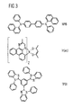
- FIG. 3 shows the structure of three organic compounds as they can be used for example in an OLED.
- the first structural formula shows NPB (N, N'-di (naphthyl-1-yl) -N-N'-diphenylbenzidine) which is useful, for example, as a hole transporting layer and matrix for emitting substances.
- the second structural formula shows Ir (ac) (iridium (III) bis (2-methyldibenzo [f, h] quinoxaline) (acetylacetonate)).
- the Ir complex can be used, for example, as a red phosphorescent dye in an OLED.
- the third structural formula shows TPBI (1,3,5-tris (1-phenyl-1H-benzimidazol-2-yl) benzene), the organic compound III.
- This compound can be used inter alia for the hole-blocking layer as well as for the electron-conducting layer 3.
- FIG. 4 schematically shows the energy levels of the individual layers of an embodiment of a device according to the invention, which is designed as an OLED.
- the LUMOs and HOMOs of the individual layers are given, as are the layer thicknesses of the individual layers.
- the transparent anode, which is made of ITO, is followed by a 30 nm thick layer of NPB.
- This first layer of NPB, which performs the function of hole transport, is followed by another layer in which NPB serves as the matrix material.
- This second layer of NPB is 7 nm thick and additionally has a proportion of 10 mol% iridium (III) bis (2-methyldibenzo [f, h] quinoxaline) (acetylacetonate) (Ir (ac)), whose structural formula in FIG. 3 is shown.
- Both the LUMO and the HOMO of the phosphorescent substance Ir (ac) are just below the corresponding energy levels of the matrix material NPD.
- the emitting layer is followed by a 10 nm thick layer of TPBI, the organic compound III. This layer has a hole blocking function.
- the energy levels of TPBI are each below the corresponding energy levels of the phosphorescent substance.
- the hole-blocking layer is followed by the electron-conducting layer (ETL).
- the electron-conducting layer in the embodiments according to the invention comprises a metal complex and an organic compound. This electron-conducting layer is obtainable by coevaporation of the metal complex with the organic compound.
- the electron-conducting layer in this embodiment performs the function of both the electron-injecting layer and the electron-transporting layer.
- the energy levels of the electron-conducting layer are above the corresponding energy levels of the hole-blocking layer.
- the electron-conducting layer is followed by a cathode made of Al. If voltage is now applied to the anode and the cathode, holes are induced by the anode and electrons are induced by the cathode into the hole-transporting or electron-transporting layer.
- the holes From there migrate the positive charge carriers, the "holes" and the Electrons in the NPB layer, which is doped with the phosphorescent material. Upon recombination of the holes and the electrons on the red emitter excitons are formed, which can excite the phosphorescent substance for emission.
- FIGS. 5 to 8 are measured curves of both inventive embodiments with metal complex in the ETL, as well as not inventive variants without metal complex in the ETL shown.
- the ETL is varied in each case.
- FIG. 5 shows three traces (21, 22, 23) in which the current density J is plotted against the voltage U.
- three OLED devices were fabricated from a 120 nm thick indium tin oxide electrode each followed by a 150 nm thick electron-conducting layer on which a 150 nm-thick Al electrode is arranged.
- the same organic compound namely the organic compound of structure V, was used for all three measurements for the electron-conducting layers 3 of the three components.
- a proportion of 10 mol% of W 2 (TBD-A) 4 is present in the organic compound V as a metal complex.
- the proportion of W 2 (TBD-A) 4 as a metal complex is only 1 mol%.
- the measurement curve 23 was carried out with the pure organic compound V, ie without a metal complex.
- the graph shows that even with a proportion of 1 mol% (curve 22) on the metal complex at higher voltages very good current densities can be achieved. Even at low voltage, the current densities, which are already achieved with 1 mol% of the metal complex (curve 22) are already significantly better than the current densities, which with the pure organic compound be achieved (trace 23).
- FIG. 5 hereby clearly shows the influence of the metal complex on the current density.
- the "free" electrons additionally provided by the metal complex can thus make a decisive contribution to the electron transport in the OLED component.
- FIG. 6 shows three measurement curves (31, 32, 33) in which the luminescence L is plotted against the voltage U.
- three components were manufactured whose structure corresponds to the structure, as in the comments on FIG. 4 describe is.
- the material for the electron-conducting layer was varied in each case.
- an electron-conducting layer of the organic compound II with a proportion of 10 mol% of W 2 (TBD-A) 4 was used.
- an electron-conducting layer of the organic compound I with a proportion of 10 mol% of W 2 (TBD-A) 4 was used.
- FIG. 7 shows three measurement curves (41, 42, 43) in which the radiation efficiency E is plotted against the luminescence L.
- the structure of the components that were used for these curves corresponds to the structure as in the comments on FIG. 4 describe is.
- the materials of the electron-conducting layer were varied from measurement curve to measurement curve.
- a device having an electron-conducting layer of the organic compound I in a proportion of 10 mol% of W 2 (TBD-A) 4 was used.
- TBD-A a device with an electron-conducting layer of the organic compound II with a proportion of 10 mol% of W 2
- the component of the measurement curve 43 additionally comprises a layer of LiF with a thickness of 0.7 nm between the electron-conducting layer and the Al electrode
- FIG. 7 can be clearly seen, the measurement curves 41 and 42, in which the electron-conducting layer in addition to the organic compound each additionally have a content of 10 mol% of the metal complex, a significantly improved efficiency over the trace 43 with the electron-conducting layer, the no metal complex includes. From the measured values in FIG. 7 Thus, it can be clearly seen that the efficiency of the component through the Metal complex which has been evaporated together with the organic compound, can be significantly increased.
- FIG. 8 shows three measurement curves (51, 52, 53) in which the luminescence L is plotted against the time t.
- the "lifetime" is defined as the 50% value of the originally set brightness, in this case 1000 cd / m 2 . If a component falls below the threshold value of 500 cd / m 2, then it is no longer usable, its "lifetime" is considered to have expired.
- components were used whose structure corresponds to the structure, as in the figure description to FIG. 4 describe is.
- the electron-conducting layer was varied in each case. In the measuring curve 51, a component was used in which the electron-conducting layer consists only of the organic compound I.
- the device additionally has between the electron-conducting layer and the Al electrode, a further layer of a thickness of 0.7 nm LiF.
- an electron-conducting layer of the organic compound I in a proportion of 10 mol% of W 2 (TBD-A) 4 was used.
- a device having an electron-conducting layer of the organic compound II with a proportion of 10 mol% of W 2 (TBD-A) 4 was used.
- FIG. 8 clearly shows that in the two measurement curves 52 and 53, in which the electron-conducting layer has a metal complex, significantly better lifetimes were achieved, as in the measurement curve 51, in which the electron-conducting layer has no metal complex. In this measurement could be achieved in the measurement curve 53 with the organic compound II again significantly better lifetimes (> 2500 h), as in the curve 52 with the organic compound I (235 h).
- the measured curves shown clearly show that the presence of the metal complex, which was vaporized together with the organic compound to form an electron-conducting layer, has a positive influence on the respectively measured electrical and optoelectronic parameters. It was possible in the corresponding organic electronic components, a higher current density, higher luminescence, better efficiency and longer life by the co-evaporation of the metal complex with the organic compound can be achieved.
- FIG. 9 shows a schematic side view of an embodiment of a device according to the invention, which is designed as an organic field effect transistor (OFET).
- OFET organic field effect transistor
- the first electrode 2 is arranged, which is formed as a gate electrode layer.
- the first electrode 2 is followed by an insulator layer 60, which may comprise, for example, a dielectric.
- the second electrode 4 is formed as source-drain contact layers and comprises an electron-conducting layer.
- a semiconductor 80 is arranged, which consists of a hole-conducting material.
- the organic field effect transistor further comprises a cover layer 70, which may serve for example for encapsulation.
Description
Es wird ein organisches elektronisches Bauelement nach dem Anspruch 1 angegeben.An organic electronic component according to
Ein weit verbreitetes Problem in organischen elektronischen Bauelementen ist es eine Schicht bereitzustellen, welche eine sehr hohe Elektronenleitfähigkeit besitzt. Die Elektronenleitfähigkeit in dem Bauelement ist oft die ausschlaggebende Größe für die Effizienz und Lebensdauer des Bauelements. Bei einer organischen LED (OLED) werden durch die Rekombination von Elektronen und Löchern Excitonen gebildet, welche Substanzen zur Emission von Strahlung anregen können. Bei solchen Bauelementen hängt auch die Lumineszenz direkt von der Excitonendichte ab und diese wiederum von der Rekombination von Elektronen und Löchern. In manchen Bauelementen werden zum Elektronentransport rein kristalline Schichten verwendet. Diese rein kristallinen Schichten haben den Nachteil, dass sie Bereiche unterschiedlicher Leitfähigkeit aufweisen. Dies hat zur Folge, dass die Ladungsträger immer den Weg des kleinsten Widerstandes wählen. Somit kommt es zum ungleichmäßigen Elektronenfluss in dieser Schicht. An den Stellen, wo ein deutlich erhöhter Elektronenfluss auftritt, kann es zu Überhitzung in der Schicht kommen und somit zur Schädigung.A common problem in organic electronic devices is to provide a layer that has very high electron conductivity. The electronic conductivity in the device is often the determining factor for the efficiency and lifetime of the device. In an organic LED (OLED) excitons are formed by the recombination of electrons and holes, which can excite substances for the emission of radiation. In such devices, the luminescence also depends directly on the density of the exciton, which in turn depends on the recombination of electrons and holes. In some devices, purely crystalline layers are used for electron transport. These purely crystalline layers have the disadvantage that they have regions of different conductivity. This has the consequence that the charge carriers always choose the path of the smallest resistance. This leads to uneven electron flow in this layer. At the points where a significantly increased flow of electrons occurs, overheating of the layer can occur and thus damage.
Im Fall von elektrolumineszierenden Bauelementen führt dieser ungleicher Elektronenfluss des Weiteren zu einer inhomogenen Abstrahlung. In den Bereichen wo ein höherer Elektronenfluss auftritt und mehrere Excitonen gebildet werden, emittiert das Bauelement mehr Strahlung und ist somit heller als in den Bereichen wo ein niedriger Elektronenfluss vorliegt.In the case of electroluminescent components, this unequal electron flow furthermore leads to an inhomogeneous emission. In areas where a higher electron flow occurs and multiple excitons are formed, the device emits more radiation and is therefore brighter than in areas where there is a low electron flux.
In der
Eine Aufgabe von Ausführungsformen der Erfindung besteht darin, eine elektronenleitende Schicht in einem organischen elektronischen Bauelement bereitzustellen, welche eine hohe Elektronenleitfähigkeit aufweist.An object of embodiments of the invention is to provide an electron-conducting layer in an organic electronic device having high electron conductivity.
Die Aufgabe wird durch ein organisches elektronisches Bauelement nach Anspruch 1 gelöst. Weitere Ausführungsformen sowie Verfahren zur Herstellung des organischen elektronischen Bauelements sind Gegenstand weiterer Patentansprüche. Gegenstand der Erfindung ist ein organischesn elektronisches Bauelement umfassend ein Substrat, eine erste Elektrode, eine zweite Elektrode, und eine elektronenleitende Schicht die so angeordnet ist, dass sie mit mindestens einer der Elektroden elektrisch leitend verbunden ist, wobei die elektronenleitende Schicht einen Metallkomplex umfasst, welcher ein Metallzentralatom und eine organische Verbindung umfasst, wobei die organische Verbindung ausgewählt ist aus:


Die elektronenleitende Schicht kann durch gemeinsames Verdampfen eines Metallkomplexes mit einer organischen Verbindung erhalten werden wobei durch das gemeinsame Verdampfen die organische Verbindung an den Metallkomplex koordiniert.The electron-conducting layer can be obtained by coevaporation of a metal complex with an organic compound, whereby co-evaporation coordinates the organic compound to the metal complex.
Durch das gemeinsame Verdampfen des Metallkomplexes mit einer organischen Verbindung wechselwirken diese beiden Verbindungen in der Gasphase oder beim zusammentreffen auf der Substratoberfläche untereinander. Diese Wechselwirkung führt zu einer Koordination der Verbindungen untereinander. Die Verbindungen werden im koordinierten Zustand abgeschieden, so dass eine Schicht ausgebildet wird, in der eine Nahordnung vorliegt. Unter Nahordnung ist zu verstehen, dass nicht die gesamte Schicht an sich kristallin ist, aber um den Metallkomplex in seinem direkten Umfeld die organischen Verbindungen nach einem bestimmten Muster angeordnet sind, welches von dem gewählten Metallkomplex und der organischen Verbindung abhängt. Die gesamte Schicht an sich ist jedoch amorph und weist somit keine Fernordnung auf.By coevaporation of the metal complex with an organic compound, these two compounds interact with one another in the gas phase or on the substrate surface. This interaction leads to a coordination of the compounds with each other. The compounds are deposited in the coordinated state, so that a layer is formed in which there is a Nahordnung. By short order is to be understood that not the entire layer is intrinsically crystalline, but around the metal complex in its immediate vicinity the organic compounds are arranged according to a specific pattern, which depends on the chosen metal complex and the organic compound. However, the entire layer itself is amorphous and thus has no long-range order.
Über die Koordination der organischen Verbindung an den Metallkomplexe, und der damit verbundenen Überlappung der Orbitale, können über einen Metallkomplex-Liganden-Elektronentransfer zusätzliche Elektronen vom Metall auf den Liganden übertragen werden (Metall-Ligand-Charge-Transfer-Komplex). Diese Elektronen können für den Elektronentransport im organischen elektronischen Bauelement zur Verfügung stehen. Durch die Erhöhung der "freien" Elektronen wird die Elektronenleitfähigkeit im Bauelement deutlich verbessert. Dies führt zu einer Erhöhung der Effizienz und der Lebensdauer des organischen elektronischen Bauelements.By coordination of the organic compound to the metal complexes, and the associated overlap of the orbitals, additional electrons can be transferred from the metal to the ligand via a metal complex-ligand electron transfer (metal-ligand charge transfer complex). These electrons may be available for electron transport in the organic electronic device. By increasing the "free" electrons, the electron conductivity in the device is significantly improved. This leads to an increase in the efficiency and the lifetime of the organic electronic component.
Die Koordination der organischen Verbindung an das Zentralatom kann direkt über ein weiteres Atom erfolgen oder aber auch über ein aromatisches System. Bei oder nach der Koordination der organischen Verbindung wird vorzugsweise keiner der zuvor vorhandenen Liganden des Metallkomplexes abgespalten, es findet also kein Ligandenaustausch statt. Der Metallkomplex ist also in der Lage weitere zusätzliche Liganden aufzunehmen und weist damit am Zentralatom freie Koordinationsstellen auf, die durch weitere Liganden belegt werden können.The coordination of the organic compound to the central atom can be done directly via another atom or else via an aromatic system. During or after the coordination of the organic compound, preferably none of the previously present ligands of the metal complex are cleaved off, so that no ligand exchange takes place. The metal complex is thus able to accommodate additional ligands and thus has on the central atom free coordination sites that can be occupied by other ligands.
In diesem Zusammenhang sei auf eine Schrift von F.A. Cotton verwiesen (
In einer weiteren Ausführungsform des organischen elektronischen Bauelements umfasst der Metallkomplex mehr als ein Zentralatom.In a further embodiment of the organic electronic component, the metal complex comprises more than one central atom.
Das Vorhandensein von mehr als einem Zentralatom verbessert die Möglichkeit, dass mehrere organische Verbindungen gleichzeitig an den Metallkomplex koordinieren. Vorzugsweise weist der Metallkomplex zwei Metallzentralatome auf. In diesem Fall weißt jedes der beiden Zentralatome eine Koordinationsstelle auf, ohne dass es zur sterischen Behinderung kommt. Die beiden Zentralatome des Metallkomplexes können hierbei untereinander wechselwirken oder auch nicht. Metallkomplexe mit zwei Zentralatomen eignen sich besonders gut zur Ausbildung von Ketten. In diesem Zusammenhang ist nochmals auf die Publikation von Cotton in Organometallics verwiesen. Hier wird die Kettenbildung eines Metallkomplexes mit zwei Rhodiumzentralatomen betrachtet. Es ist eine kettenartige Abfolge von Metallkomplexen und von zwei benachbarte Komplexe verbrückenden Aromaten dargestellt. Hierbei steht der Aromat senkrecht zwischen den Metallkomplexen, und die Rh-Rh-Achse senkrecht auf dem Aromaten. Für eine erfindungsgemäße Ausführungsform sind die Metallkomplexe mit zwei Zentralatomen, die in der Verlängerung der Zentralatomachse noch keine Liganden aufweisen, bevorzugt, so dass das Zentralatom noch zwei freie bevorzugt gegenüberliegende Koordinationsstellen aufweist. Dies ist beispielsweise für den Rhodiumkomplex in der Publikation von Cotton gegeben. Für solche Metallkomplexe ist es aus sterischen Gründen besonders einfach, in Verlängerung der Zentralatomachse an beiden gegenüberliegenden Seiten zusätzliche Liganden anzulagern.The presence of more than one central atom enhances the possibility of multiple organic compounds simultaneously coordinating to the metal complex. Preferably, the metal complex has two central metal atoms. In this case, each of the two central atoms has a coordination point without steric hindrance. The two central atoms of the metal complex can or do not interact with each other. Metal complexes with two central atoms are particularly suitable for the formation of chains. In this connection, reference is again made to the publication by Cotton in Organometallics. Here the chain formation of a metal complex with two rhodium central atoms is considered. It is shown a chain-like sequence of metal complexes and of two adjacent complexes bridging aromatics. Here, the aromatic is perpendicular between the metal complexes, and the Rh-Rh axis perpendicular to the aromatic. For an embodiment according to the invention, the metal complexes with two central atoms, which do not yet have any ligands in the extension of the central atom axis, are preferred, so that the central atom still has two free, preferably opposite, coordination sites. This is for example given for the rhodium complex in the publication by Cotton. For steric reasons, it is particularly easy for such metal complexes to attach additional ligands in extension of the central axis on both opposite sides.
Eine Ausführungsform des organischen elektronischen Bauelements ist das Zentralatom oder sind die Zentralatome ausgewählt aus: Cr, Mo oder W.An embodiment of the organic electronic device is the central atom or the central atoms are selected from: Cr, Mo or W.
Hierbei ist W ein bevorzugtes Metallzentralatom. Besonders bevorzugt ist es, wenn alle Zentralatome im Metallkomplex W sind. Elemente Cr, Mo und W erweisen sich aus zwei Gründen als besonders vorteilhaft. Zum einen verfügen sie über die Möglichkeit mit zusätzlichen Liganden eine Koordination einzugehen, zum anderen haben ihre Metallkomplexe bei geeigneter Wahl der Liganden eine sehr niedrige Ionisationsenthalpie. Dies bedeutet, dass diese Metallkomplexe über eine hohe Bereitschaft und Möglichkeit verfügen, "freie" Elektronen bereitzustellen. Diese Elektronen können beispielsweise auf die zusätzlich gebundenen Liganden übertragen werden. Über diese Koordination und den damit verbundenen Metallkomplex-Ligand-Elektronentransfer (charge-transfer-complex) können der elektronenleitenden Schicht zusätzliche Elektronen zum Ladungstransport zur Verfügung gestellt werden. Über diesen Elektronen kann der Ladungstransport im organischen elektronischen Bauelement gesteigert werden was die Effizienz des Bauelements steigert. In diesem Zusammenhang sei auf eine Publikation von F.A. Cotton (
Cotton zeigt in seiner Publikation, dass dieser Komplex zu den Verbindungen gehört, deren Elektronenkonfiguration geschlossene also aufgefüllte Elektronenschalen aufweist und trotzdem über ein extrem niedriges Ionisationspotential verfügt. Cotton zeigt des Weiteren, dass die Zentralatome in diesem Komplex sehr hohe Oxidationsstufen einnehmen können. Somit können von den beiden W-Zentralatomen viele Elektronen abgegeben werden. In einer weiteren Publikation von Cotton (
Beschrieben wird auch ein organisches elektronisches Bauelement wobei die organische Verbindung einen Heteroaromaten umfasst.Also described is an organic electronic device wherein the organic compound comprises a heteroaromatic.
Vorzugsweise umfasst die organische Verbindung mehr als einen Heteroaromaten. Dies ermöglicht es der organischen Verbindung an mehrere Metallkomplexe gleichzeitig zu koordinieren. Ein Heteroaromat hat gegenüber einem Aromaten den Vorteil, dass dieser nicht nur über das aromatische System (π-Elektronen) an ein Metallkomplex koordinieren kann, wie es in der Publikation von Cotton in Organometallics beschrieben wird, welche oben zitiert ist, sondern dass des Weiteren die Koordination auch direkt über das Heteroatom erfolgen kann.Preferably, the organic compound comprises more than one heteroaromatic. This allows the organic compound to coordinate to several metal complexes simultaneously. A heteroaromatic has the advantage over an aromatic that it can coordinate not only via the aromatic system (π-electrons) to a metal complex, as described in the publication of Cotton in Organometallics, which is cited above, but that further Coordination can also take place directly via the heteroatom.
Je größer also die Anzahl der Heteroaromaten in der organischen Verbindung ist, desto größer ist die Anzahl der möglichen Koordinationsstellen für einen Metallkomplex. Hierbei ist N ein bevorzugtes Heteroatom. N weist aufgrund des meist freien Elektronenpaares ein sehr gutes Koordinationsvermögen gegenüber Metallkomplexen auf.Thus, the larger the number of heteroaromatics in the organic compound, the greater the number of possible coordination sites for a metal complex. Here, N is a preferred heteroatom. Due to the mostly lone pair of electrons, N has a very good coordination capacity with respect to metal complexes.
Weiterhin dargelegt ist ein organisches elektronisches Bauelement wobei die organische Verbindung einen Heteroaromaten umfasst, welcher über eine C-C-Bindung mit einem Aromaten konjugiert ist.Further set forth is an organic electronic device wherein the organic compound comprises a heteroaromatic which is conjugated via a C-C bond with an aromatic.
Unter C-C-Bindung ist eine Kohlenstoff-Kohlenstoff-Einfachbindung zu verstehen, der Heteroaromat und der Aromat sind also nicht kondensiert. Ein derartiges System, bei dem der Heteroaromat mit weiteren Aromaten über C-C-Einfachbindungen verknüpft ist, hat gegenüber den kondensierten Systemen den Vorteil, dass es sterisch nicht so anspruchsvoll und voluminös ist, und somit leichter an einen Metallkomplex koordinieren kann, beziehungsweise besser an mehrere Metallkomplexe gleichzeitig koordinieren kann. Das Heteroatom im Heteroaromat ist vorzugsweise N, O oder S, wobei N besonders bevorzugt ist.By C-C bond is meant a carbon-carbon single bond, the heteroaromatic and the aromatic are thus not condensed. Such a system, in which the heteroaromatic is linked to other aromatics via CC single bonds, has the advantage over the condensed systems that it is not sterically so demanding and voluminous, and thus can coordinate more easily to a metal complex, or better to several metal complexes can coordinate at the same time. The heteroatom in the heteroaromatic is preferably N, O or S, with N being particularly preferred.
Darüber hinaus beschrieben ist ein organisches elektronisches Bauelement, wobei die organische Verbindung nur Heteroaromaten umfasst, welche keine kondensierten Systeme ausbilden. Die Heteroaromaten sind also nicht mit anderen heteroaromatischen oder aromatischen Systemen kondensiert. Auch hier ergibt sich wieder der sterische Vorteil der nicht-kondensierten Systeme gegenüber den kondensierten Systemen. Das Heteroatom im Heteroaromat ist vorzugsweise N, O oder S, wobei N besonders bevorzugt ist.In addition, an organic electronic device is described, wherein the organic compound comprises only heteroaromatics, which do not form condensed systems. The heteroaromatics are therefore not condensed with other heteroaromatic or aromatic systems. Again, there is again the steric advantage of the non-condensed systems over the condensed systems. The heteroatom in the heteroaromatic is preferably N, O or S, with N being particularly preferred.
Beschrieben ist auch ein organisches elektronisches Bauelement wobei die organische Verbindung nur Heteroaromaten mit einem oder zwei Heteroatomen umfasst. Unter Heteroaromat ist ein gesamtes kondensiertes System zu verstehen. Das Heteroatom bzw. die Heteroatome im Heteroaromat sind vorzugsweise N, O oder S, wobei N besonders bevorzugt ist.Also described is an organic electronic device wherein the organic compound comprises only heteroaromatic compounds having one or two heteroatoms. Heteroaromatic means an entire condensed system. The heteroatom or heteroatoms in the heteroaromatic are preferably N, O or S, with N being particularly preferred.
Genannt ist darüber hinaus ein organisches elektronisches Bauelement, wobei die organische Verbindung nur Heteroaromaten umfasst, deren Ringe aus sechs Atomen gebildet werden. Über diese Heteroaromaten kann in Konjugation mit anderen Heteroaromaten oder Aromaten am besten ein delokalisiertes π-Elektronensystem aufgebaut werden, welches gut in der Lage ist zusätzliche Ladung aufzunehmen. Das Heteroatom im Heteroaromat ist vorzugsweise N, O oder S, wobei N besonders bevorzugt ist.Also mentioned is an organic electronic device, wherein the organic compound comprises only heteroaromatics whose rings are formed from six atoms. In conjugation with other heteroaromatics or aromatics, these deletions can best be used to construct a delocalized π-electron system that is well able to accept additional charge. The heteroatom in the heteroaromatic is preferably N, O or S, with N being particularly preferred.
Beschrieben wird zudem ein organisches elektronisches Bauelement, wobei die organische Verbindung die folgende allgemeine Formel aufweist:

- stehen die Ringglieder A bis F unabhängig voneinander für C oder eines oder zwei Ringglieder können N sein,
n ist 2bis 8, wobei die freien Valenzen der Enden jeweils unabhängig voneinander durch H, Methyl, Phenyl, 2-Pyridyl, 3-Pyridyl bzw. 4-Pyridyl abgesättigt sein können,- R1 bis R4 können jeweils unabhängig voneinander H, Methyl, Phenyl, 2-Pyridyl, 3-Pyridyl bzw. 4-Pyridyl sein und / oder R1 und R2 bzw. R3 und R4 können miteinander durch Butadien bzw. Azabutadieneinheiten verbunden sein, so dass ein Sechsring ausgebildet wird, sowie zwischen dem n-ten und (n+1)-ten Ring durch Ethylen- bzw. Azomethineinheiten verbunden sein, wobei Phenanthren- bzw. Azaphenanthreneinheiten gebildet werden.
- are the ring members A to F independently of each other for C or one or two ring members can be N,
- n is 2 to 8, wherein the free valencies of the ends may each be independently saturated by H, methyl, phenyl, 2-pyridyl, 3-pyridyl or 4-pyridyl,
- R 1 to R 4 may each independently be H, methyl, phenyl, 2-pyridyl, 3-pyridyl or 4-pyridyl and / or R 1 and R 2 or R 3 and R 4 may each other by butadiene or azabutadiene be connected so that a six-membered ring is formed, as well as between the n-th and (n + 1) -th ring by ethylene or Azomethineinheiten be connected to Phenanthren- or Azaphenanthreneinheiten are formed.
Verbindungen mit dieser allgemeinen Formel können an Metallkomplexe koordinieren. Des Weiteren eignen sich Verbindungen dieser allgemeinen Formel zur Einstellung des Farbeindrucks des organischen elektronischen Bauelements im ausgeschalteten Zustand.Compounds of this general formula can coordinate to metal complexes. In addition, compounds of this general formula are suitable for adjusting the color impression of the organic electronic component in the switched-off state.
Durch eine geeignete Wahl des Metallkomplexes und der organischen Verbindung kann ein vorbestimmter Farbeindruck für das gewünschte äußere Erscheinungsbild zumindest im ausgeschalteten elektronischen Betriebszustand gewährleistet werden. Dies kann durch Ausbildung von Charge-Transfer-Komplexen in der elektronenleitenden Schicht möglich sein. Dabei bilden die Metallkomplexe und die organischen Verbindungen Elektronen-Donor-Akzeptor-Komplexe, deren Absorptionsbande vorzugsweise im sichtbaren Wellenlängenbereich liegen. Die Absorptionsbande der Charge-Transfer-Komplexe hängt dabei von der jeweiligen energetischen Lage ihrer HOMOs und LUMOs relativ zueinander ab. Die Charge-Transfer-Komplexe können somit einen vorbestimmten Farbeindruck ermöglichen.By a suitable choice of the metal complex and the organic compound, a predetermined color impression for the desired external appearance can be ensured at least in the switched-off electronic operating state. This may be possible by forming charge-transfer complexes in the electron-conducting layer. The metal complexes and the organic compounds form electron-donor-acceptor complexes whose absorption bands are preferably in the visible wavelength range. The absorption band of the charge-transfer complexes depends on the respective energetic position of their HOMOs and LUMOs relative to each other. The charge-transfer complexes can thus enable a predetermined color impression.
Diese Verbindungen weisen zusätzlich gute Ladungstransporteigenschaften auf, welche sich über die Anzahl der Stickstoffatome im Ringsystem steuern lassen.These compounds additionally have good charge transport properties, which can be controlled by the number of nitrogen atoms in the ring system.
Die Absorptionsbande der durch Kokondensation gebildeten Komplexe beeinflusst gezielt den entstehenden Farbeindruck des Bauelements im ausgeschalteten Zustand.The absorption band of the complexes formed by cocondensation selectively influences the resulting color impression of the component in the switched-off state.
Die Oligo-pyridyl-und/oder-pyrimidyl-arene sind in ihrer Anordnung frei permutierbar und können in ihrer Peripherie wiederum Phenyl, Pyridyl und Pyrimidyl sowie Wasserstoff und Methyl als Substituenten tragen. Unter Oligo soll ein Wertebereich von n = 2 bis 8 verstanden werden.The oligo-pyridyl and / or pyrimidyl-arenes are freely permutable in their arrangement and can in turn carry phenyl, pyridyl and pyrimidyl as well as hydrogen and methyl as substituents in their periphery. By oligo should be understood a range of values from n = 2 to 8.
In einer weiteren Ausführungsform des organischen elektronischen Bauelements ist die organische Verbindung ausgewählt aus:


Beschrieben sind zudem die folgenden organischen Verbindungen:


Die in den Strukturen I bis XIII dargestellten Verbindungen eignen sich besonders gut als organische Verbindung für die elektronenleitende Schicht. Jede dieser Verbindungen umfasst sowohl einen Aromaten wie auch einen Stickstoffheterozyklus. Jede dieser Verbindungen weist somit mehrere Koordinationsstellen für Metallkomplexe auf. Diese Verbindungen I bis XIII ermöglichen nicht nur die Ausbildung von zweidimensionalen Ketten, sondern durch ihre Vielzahl von Koordinationsstellen auch die Ausbildung von dreidimensionalen Netzwerken. Hierbei koordiniert eine organische Verbindung an mehr als zwei Metallkomplexe. Des Weiteren verfügen diese Verbindungen über große delokalisierte Elektronensysteme wie beispielsweise kondensierte Aromaten oder Aromaten die in elektronischer Konjugation zueinander stehen. Diese delokalisierten Elektronensysteme ermöglichen es den Verbindungen sehr gut weitere negative Ladungen aufzunehmen und zu transportieren, da diese zusätzliche Ladung einfach auf mehrere Atome im Molekül verteilt werden kann. Somit kann ein koordinierter Metallkomplex gut negative Ladung auf die an ihn koordinierte organische Verbindung übertragen. Des Weiteren können Elektronen von den organischen Verbindungen I bis XIII auch gut unter den organischen Verbindungen selbst weitergeleitet werden. Dies ist ebenfalls entscheidend für eine gute Elektronenleitfähigkeit in der elektronenleitenden Schicht.The compounds shown in structures I to XIII are particularly suitable as an organic compound for the electron-conducting layer. Each of these compounds includes both an aromatic and a nitrogen heterocycle. Each of these compounds thus has several coordination sites for metal complexes. These compounds I to XIII allow not only the formation of two-dimensional chains, but also the formation of three-dimensional networks through their multiplicity of coordination sites. Here, an organic compound coordinates to more than two metal complexes. Furthermore, these compounds have large delocalized electron systems such as fused aromatics or aromatics that are in electronic conjugation with each other. These delocalized electron systems allow the compounds to very well absorb and transport more negative charges, because this extra charge can be easily distributed to multiple atoms in the molecule. Thus, a coordinated metal complex can transfer good negative charge to the organic compound coordinated to it. Furthermore, electrons from the organic compounds I to XIII can also be well forwarded among the organic compounds themselves. This is also crucial for good electron conductivity in the electron-conducting layer.
In einer weiteren Ausführungsform des organischen elektronischen Bauelements ist die organische Verbindung ausgewählt aus:


Die in den Strukturen I, II, XIV bis XXIII dargestellten Verbindungen eignen sich besonders gut als organische Verbindung für die elektronenleitende Schicht. Jede dieser Verbindungen umfasst einen Stickstoffheterozyklus, sowie zusätzlich einen weiteren Stickstoffheterozyklus oder einen Homoaromaten, welcher aus C-Atomen aufgebaut ist. Jede dieser Verbindungen weist somit mehrere Koordinationsstellen für Metallkomplexe auf. Diese Verbindungen I, II, XIV bis XXIII ermöglichen nicht nur die Ausbildung von zweidimensionalen Ketten, sondern durch ihre Vielzahl von Koordinationsstellen auch die Ausbildung von dreidimensionalen Netzwerken. Hierbei koordiniert die organische Verbindung an mehr als zwei Metallkomplexe. Des Weiteren verfügen diese Verbindungen über große delokalisierte Elektronensysteme wie beispielsweise kondensierte Aromaten oder Aromaten die in elektronischer Konjugation zueinander stehen. Diese delokalisierten Elektronensysteme ermöglichen es den Verbindungen sehr gut weitere negative Ladungen aufzunehmen und zu transportieren, da diese zusätzliche Ladung einfach auf mehrere Atome im Molekül verteilt werden kann. Somit kann ein koordinierter Metallkomplex gut negative Ladung auf die an ihn koordinierte organische Verbindung übertragen. Des Weiteren können Elektronen von den organischen Verbindungen I, II, XIV bis XXIII auch gut unter den organischen Verbindungen selbst weitergeleitet werden. Dies ist ebenfalls entscheidend für eine gute Elektronenleitfähigkeit in der elektronenleitenden Schicht.The compounds shown in structures I, II, XIV to XXIII are particularly suitable as an organic compound for the electron-conducting layer. Each of these compounds comprises a nitrogen heterocycle, as well as an additional nitrogen heterocycle or a homoaromatic, which is composed of carbon atoms. Each of these compounds thus has several coordination sites for metal complexes. These compounds I, II, XIV to XXIII not only allow the formation of two-dimensional chains, but also the formation of three-dimensional networks through their multiplicity of coordination sites. Here, the organic compound coordinates to more than two metal complexes. Furthermore, these compounds have large delocalized electron systems such as fused aromatics or aromatics that are in electronic conjugation with each other. These delocalized electron systems make it very easy for the compounds to accept and transport further negative charges, since this extra charge can be easily distributed over several atoms in the molecule. Thus, a coordinated Metal complex well negative charge transferred to him coordinated organic compound. Furthermore, electrons from the organic compounds I, II, XIV to XXIII can also be well forwarded among the organic compounds themselves. This is also crucial for good electron conductivity in the electron-conducting layer.
In einer Ausführungsform des organischen elektronischen Bauelements verbrücken zumindest Teile der organischen Verbindungen zwei Metallkomplexe miteinander, so dass eine kettenartige Struktur ausgebildet wird und/oder verbrücken zumindest Teile der organischen Verbindungen mehr als zwei Metallkomplexe miteinander, so dass eine netzartige Struktur ausgebildet wird.In one embodiment of the organic electronic component, at least parts of the organic compounds bridge two metal complexes with one another, so that a chain-like structure is formed and / or at least parts of the organic compounds bridge more than two metal complexes with one another, so that a net-like structure is formed.
Durch geeignete Wahl der Metallkomplexe zum Beispiel zweikernige Metallkomplexe und geeignete Wahl der organischen Verbindungen wie beispielsweise die Verbindungen I bis XXIII kommt es durch das gemeinsame Verdampfen des Metallkomplexes mit der organischen Verbindung in der Gasphase bzw. auf der abgeschiedenen Oberfläche zu Wechselwirkungen, so dass die Verbindungen aneinander koordinieren. Die Koordination bleibt auch bei der Ausbildung der elektronenleitenden Schicht erhalten. Diese Koordination kann zur Ausbildung von zweidimensionalen Ketten oder dreidimensionalen Netzen führen. Diese Ketten oder Netze werden als solche im Verdampfungsprozess abgeschieden und liegen auch als solche in der elektronenleitenden Schicht im organischen elektronischen Bauelement vor. Die Ausbildung von ketten- oder netzartigen Strukturen ermöglicht es, das von den Metallkomplexen zusätzliche Elektronen auf die organischen Verbindungen übertragen werden können, welche dann für den Ladungstransport in der elektronenleitenden Schicht zur Verfügung stehen. In diesem Zusammenhang ist auf eine Publikation von F.A. Cotton (
In einer Ausführungsform des organischen elektronischen Bauelements ist die elektronenleitende Schicht amorph und weist eine mikro- bis nanokristalline Nahstruktur auf.In one embodiment of the organic electronic component, the electron-conducting layer is amorphous and has a micro- to nano-crystalline near structure.
Scheidet man organische Verbindungen, wie sie beispielsweise für elektronenleitende Schichten verwendet werden, über Verdampfung ab, so kann es zur Kristallisation der organischen Verbindungen kommen. Eine rein kristalline elektronenleitende Schicht hat sich als nachteilig erwiesen, da diese Schicht Bereiche unterschiedlicher Leitfähigkeit aufweist. Durch das Anlegen einer Spannung entstehen somit in der Schicht unterschiedliche Stromdichten. In Bereichen mit sehr hohen Stromdichten kann es zu Überhitzung und zu Beschädigung der elektronenleitenden Schicht kommen. Im Fall von lichtemittierenden Bauelementen führte die unterschiedliche Leitfähigkeit zusätzlich zu einer inhomogenen Abstrahlung. Das Problem wird durch eine makroskopisch bis nanoskopisch amorphe elektronenleitende Schicht gemindert. Eine solche Schicht ist erhältlich durch das gemeinsame Verdampfen der organischen Verbindung mit einem Metallkomplex, wobei die organische Verbindung an den Metallkomplex koordiniert und dadurch die Kristallisation unterbindet. Durch den Metallkomplex muss aber sichergestellt werden, dass die jetzt makroskopisch bis nanoskopisch amorphe Struktur immer noch gute elektronenleitende Eigenschaften besitzt. Dies kann beispielsweise dadurch geschehen, dass die zusätzliche Verbindung zusätzliche Ladungsträger bereitstellt. Eine organische Verbindung, welche an den Metallkomplex koordiniert und somit mikrokristalline Strukturen ausbildet, ist in der Lage zusätzliche Ladungsträger, welche vom Zentralatom bereitgestellt werden, aufzunehmen. Somit wird die gegenüber der kristallinen Schicht reduzierte Mobilität der Ladungsträger durch eine Erhöhung der Anzahl der Ladungsträger kompensiert. Ein organisches elektronisches Bauelement, beispielsweise eine OLED, welche eine solche Schicht umfasst, leuchtet homogen. An den Korngrenzen von OLED-Vorrichtungen, die makrokristalline Schichten aufweisen ändern sich die Leitfähigkeiten, so dass es zu einem inhomogenen Leuchtbild kommt bzw. beispielsweise eine LED durch Überstrom an gewissen Stellen zerstört wird.If organic compounds, such as those used for example for electron-conducting layers, are deposited by evaporation, the organic compounds may crystallize. A purely crystalline electron-conducting layer has proven to be disadvantageous since this layer has regions of different conductivity. By applying a voltage thus arise in the layer different current densities. In areas with very high current densities, overheating and damage to the electron-conducting layer may occur. In the case of light-emitting components, the different conductivity additionally led to an inhomogeneous emission. The problem is mitigated by a macroscopic to nanoscopic amorphous electron-conducting layer. Such a layer is obtainable by co-evaporation of the organic compound with a metal complex, whereby the organic compound coordinates to the metal complex and thereby inhibits crystallization. However, the metal complex must ensure that the macroscopic to nanoscopic amorphous structure still has good electron-conducting properties. This can be done, for example, by the additional connection providing additional charge carriers. An organic compound which coordinates to the metal complex and thus forms microcrystalline structures is capable of accepting additional charge carriers provided by the central atom. Thus, the reduced mobility of the charge carriers compared to the crystalline layer is compensated by an increase in the number of charge carriers. An organic electronic component, for example an OLED, which comprises such a layer, shines homogeneously. At the grain boundaries of OLED devices, which have macrocrystalline layers, the conductivities change, so that an inhomogeneous luminous image or, for example, an LED is destroyed by overcurrent at certain points.
In einer Ausführungsform des organischen elektronischen Bauelements umfasst die elektronenleitende Schicht keine strahlungsemittierenden Substanzen.In one embodiment of the organic electronic component, the electron-conducting layer does not comprise any radiation-emitting substances.
Somit kann bei dieser Ausführungsform aus der elektronenleitenden Schicht keine Strahlung emittiert werden. Weder die organische Verbindung noch der Metallkomplex sind bei dieser Ausführungsform in der Lage Strahlung zu emittieren.Thus, in this embodiment, no radiation can be emitted from the electron-conducting layer. Neither the organic compound nor the metal complex are capable of emitting radiation in this embodiment.
Eine Ausführungsform des organischen elektronischen Bauelements umfasst einen Metallkomplex dessen HOMO (highest occupied molecular orbital) näher an seiner Ionisationsenergie liegt, als das LUMO (lowest unoccupied molecular orbital) organischen Verbindung, welche zusätzlich an den Metallkomplex koordiniert.One embodiment of the organic electronic device comprises a metal complex whose HOMO (highest occupied molecular orbital) is closer to its ionization energy than the LUMO (lowest unoccupied molecular orbital) organic compound, which additionally coordinates to the metal complex.
Dies ermöglicht es, dass auch die Metallkomplexe, die eine abgeschlossene Elektronenstruktur besitzen, Elektronen über Komplex-Liganden-Ladungstransfer vom Komplex auf den Liganden übertragen. Diese übertragenen Elektronen leisten einen wesentlichen Beitrag zur Elektronenleitfähigkeit der elektronenleitenden Schicht. In diesem Zusammenhang sei nochmals auf die Publikation von Cotton in Science, welche bereits in einem vorangehenden Abschnitt diskutiert wurde, verwiesen. In dieser Publikation beschreibt Cotton die extrem niedrige Ionisierungsenthalpie von Komplexen der allgemeinen Formel M2(TBD-A)4, wobei in der Publikation das Zentralatom M ausgewählt ist aus Cr, Mo oder W. TBD-A steht für das Anion von 1,5,7-Triazabicyclo[4.4.0]dec-5-ene. Cotton führt in seiner Publikation eine genauere Betrachtung der Orbitale des Metallkomplexes sowie des TBD-A-Liganden durch. Hierbei zeigt er, dass die niedrige Ionisationsenthalpie unter anderem in der Lage des HOMOs des Metallkomplexes relativ zum LUMO des TBD-A-Liganden begründet liegt.This makes it possible for the metal complexes, which have a closed electronic structure, to transfer electrons from the complex to the ligand via complex-ligand charge transfer. These transferred electrons make a significant contribution to the electronic conductivity of the electron-conducting layer. In this context, reference should once again be made to the publication by Cotton in Science, which has already been discussed in a preceding section. In this publication, Cotton describes the extremely low ionization enthalpy of complexes of the general formula M 2 (TBD-A) 4 , where in the publication the central atom M is selected from Cr, Mo or W. TBD-A stands for the anion of 1.5 , 7-triazabicyclo [4.4.0] dec-5-ene. In his publication Cotton reviews the orbitals of the metal complex and the TBD-A ligand. He shows that the low ionization enthalpy, inter alia, in the location of the HOMOs of the metal complex is due to the LUMO of the TBD-A ligand.
Das organische elektronische Bauelement ist vorzugsweise als organische LED (OLED) ausgebildet, welche eine elektrolumineszierende Schicht umfasst. Bei dem organischen elektronischen Bauelement kann es sich aber beispielsweise auch um einen organischen Feldeffekttransistor um eine organische Solarzelle oder eine organischen Fotodetektor handeln. Ein organischer Feldeffekttransistor (OFET) besitzt drei Anschlüsse: Source, Gate und Drain. Das Substrat kann hierbei als Gate-Elektrode genutzt werden. Ist dies der Fall, so folgt auf das Substrat eine Isolatorschicht, auf der der Source und Drain Anschluss angeordnet sind. Sowohl zwischen Source und Drain wie auch über beiden Anschlüssen ist eine organische Halbleiterschicht angeordnet. Bei der organischen Solarzelle sind auf einem Substrat übereinander zwei Elektroden angeordnet, zwischen denen sich eine organische, photoaktive Schicht befindet. Die photoaktive Schicht absorbiert das Licht, wodurch es in der Schicht zur Ladungstrennung kommt. Die so gebildeten Elektronen wandern zur Anode und die Löcher zur Kathode wodurch ein Stromfluss generiert wird.The organic electronic component is preferably designed as an organic LED (OLED), which comprises an electroluminescent layer. However, the organic electronic component can also be, for example, an organic field-effect transistor with an organic solar cell or an organic photodetector. An organic field effect transistor (OFET) has three terminals: source, gate and drain. The substrate can be used here as a gate electrode. If this is the case, an insulator layer follows on the substrate, on which the source and drain connection are arranged. Both an organic semiconductor layer is arranged between the source and the drain as well as over both terminals. In the organic solar cell, two electrodes are arranged one above the other on a substrate, between which there is an organic, photoactive layer. The photoactive layer absorbs the light, causing it to be in the charge separation layer. The electrons thus formed migrate to the anode and the holes to the cathode whereby a current flow is generated.
Die elektronenleitende Schicht eignet sich besonders gut für organische elektronische Bauelemente deren Effizienz unter anderem von einem guten Elektronentransport abhängt. So hängt beispielsweise bei einer OLED die Lumineszenz direkt von der Anzahl der gebildeten Excitonen ab. Diese hängt wiederum davon ab, wie viele Elektronen und Löcher rekombinieren. Ein guter Elektronen- und Lochtransport führen somit zu einer hohen Rekombinationsrate und somit zu einer guten Lumineszenz und Effizienz der OLED.The electron-conducting layer is particularly well suited for organic electronic components whose efficiency depends, inter alia, on a good electron transport. For example, in the case of an OLED, the luminescence depends directly on the number of excitons formed. This in turn depends on how many electrons and holes recombine. A good electron and hole transport thus lead to a high recombination rate and thus to a good luminescence and efficiency of the OLED.
Neben dem organischen elektronischen Bauelement selbst werden auch Verfahren zur Herstellung des organischen elektronischen Bauelements beansprucht.In addition to the organic electronic component itself, methods for producing the organic electronic component are claimed.
Eine Variante des Verfahrens zur Herstellung eines organischen elektronischen Bauelements umfasst die Verfahrensschritte Bereitstellen eines Substrates als Verfahrensschritt A), Aufbringen einer ersten Elektrode im Verfahrensschritt B), Abscheiden einer elektronenleitenden Schicht auf dem Substrat als Verfahrensschritt C), Aufbringen einer zweiten Elektrode im Verfahrensschritt D), wobei das Abscheiden der elektronenleitenden Schicht durch gleichzeitiges Verdampfen eines Metallkomplexes und einer organischen Verbindung erfolgt und
wobei beim gleichzeitigen Verdampfen die organische Verbindung in der Gasphase an den Metallkomplex koordiniert, wobei die organische Verbindung ausgewählt ist aus:


wherein, upon simultaneous evaporation, the organic compound in the gaseous phase coordinates to the metal complex, wherein the organic compound is selected from:
Durch ein solches Verfahren kann beispielsweise ein organisches elektronisches Bauelement gefertigt werden, wie es in Anspruch 1 beansprucht wird. Die elektronenleitende Schicht kann hierbei direkt auf ein Substrat abgeschieden werden oder es können zuvor auf dem Substrat andere Schichten abgeschieden werden, wie beispielsweise eine Elektrodenschicht, wobei dann die elektronenleitende Schicht auf die sich bereits auf dem Substrat befindlichen Schichten abgeschieden wird. Das Abscheiden der elektronenleitenden Schicht erfolgt durch gleichzeitiges Verdampfen eines Metallkomplexes und einer organischen Verbindung. Das gleichzeitige Verdampfen ermöglicht es den Molekülen untereinander wechselzuwirken.By such a method, for example, an organic electronic component as claimed in
In einer weiteren Verfahrensvariante koordiniert die organische Verbindung an den Metallkomplex durch das gemeinsame Verdampfen.In a further process variant, the organic compound coordinates to the metal complex by the common evaporation.
Durch das zeitgleiche Verdampfen von Metallkomplexen und organischer Verbindung liegen beide Verbindungen zeitgleich nebeneinander in der Gasphase vor. Dies ermöglicht es der organischen Verbindung an den Metallkomplex in der Gasphase zu koordinieren. Die Koordination kann beispielsweise über einen Heteroaromaten in der organischen Verbindung erfolgen. Die Koordination bleibt auch beim Abscheiden zur elektronenleitenden Schicht bestehen.Due to the simultaneous vaporization of metal complexes and organic compounds both compounds are simultaneously next to each other in the gas phase. This allows the organic compound to coordinate to the metal complex in the gas phase. The coordination can be carried out for example via a heteroaromatic in the organic compound. The coordination also persists during the deposition to the electron-conducting layer.
Es besteht aber auch die Möglichkeit, dass der Metallkomplexen und die organischer Verbindung erst auf der zu beschichtenden Oberfläche oder beim Auftreffen auf die Oberfläche aufeinandertreffen und unter Bildung der elektronenleitende Schicht die organische Verbindung an den Metallkomplex koordiniert.However, there is also the possibility that the metal complexes and the organic compound meet only on the surface to be coated or when hitting the surface and, with the formation of the electron-conducting layer, coordinate the organic compound to the metal complex.
In einer weiteren Verfahrensvariante wird die elektronenleitende Schicht als kettenartige oder netzartige Struktur abgeschieden.In a further variant of the method, the electron-conducting layer is deposited as a chain-like or net-like structure.
Durch die Koordination der organischen Verbindung an den Metallkomplex in der Gasphase können sich kettenartige oder netzartige Strukturen ausbilden. Diese kettenartigen oder netzartigen Strukturen werden dann auch als solche abgeschieden und liegen auch als solche in der elektronenleitenden Schicht im organischen elektronischen Bauelement vor.The coordination of the organic compound to the metal complex in the gas phase can form chainlike or netlike structures. These chain-like or net-like structures are then deposited as such and are also present as such in the electron-conducting layer in the organic electronic component.
Beim Auftreffen auf die Oberfläche sind die Moleküle noch soweit beweglich, dass sich die Koordinationsstellen finden und der entsprechende Energiebeitrag frei wird, d.h. es zu einer Koordination kommen kann.Upon impact with the surface, the molecules are still sufficiently mobile to find the coordination sites and release the corresponding energy contribution, i. it can come to a coordination.
In einer Verfahrensvariante wird der Grad der Vernetzung der elektronenleitenden Schicht durch das Verhältnis zwischen Metallkomplex und der organischen Verbindung beim Verdampfen gesteuert.In a variant of the method, the degree of crosslinking of the electron-conducting layer is determined by the ratio between Metal complex and the organic compound controlled during evaporation.
Je nach Verhältnis von Metallkomplex zu organischer Verbindung kann der Grad der Vernetzung und somit die Ausbildung von netzartigen oder kettenartigen Strukturen gesteuert werden. Bezugsweise wird die organische Verbindung in einen Überschuss bezogen auf das Molverhältnis zum Metallkomplex verdampft.Depending on the ratio of metal complex to organic compound, the degree of crosslinking and thus the formation of net-like or chain-like structures can be controlled. By way of example, the organic compound is vaporized to an excess based on the molar ratio to the metal complex.
Hierbei kann der Anteil des Metallkomplexes in der Schicht, welche den Metallkomplex und die organische Verbindung umfasst bei 1 bis 50 mol-% liegen, ein Anteil von 5 bis 25 mol-% ist bevorzugt, ein Anteil von 10 bis 15 mol-% besonders bevorzugt.Here, the proportion of the metal complex in the layer comprising the metal complex and the organic compound may be from 1 to 50 mol%, a proportion of from 5 to 25 mol% is preferred, and a proportion of from 10 to 15 mol% is particularly preferred ,
In einer weiteren Verfahrensvariante koordiniert die organische Verbindung vor dem Verdampfen nicht an den Metallkomplex.In a further process variant, the organic compound does not coordinate to the metal complex prior to evaporation.
Der Metallkomplex und die organische Verbindung können beispielsweise aus zwei unterschiedlichen, räumlich voneinander getrennten Vorlagen verdampft werden. Es ist jedoch auch möglich, die beiden Verbindungen in eine Vorlage zu geben, ohne das in der festen Phase eine Reaktion oder Koordination unter den Verbindungen stattfindet und das die Verbindungen dann aus der gemeinsamen Vorlage verdampft werden.The metal complex and the organic compound can be evaporated, for example, from two different, spatially separated templates. However, it is also possible to place the two compounds in a template without the reaction or coordination taking place under the compounds in the solid phase and then evaporating the compounds from the common template.
Im Folgenden sollen exemplarisch anhand eines Beispiels eine Variante eines Herstellungsverfahrens näher beschrieben werden.In the following, a variant of a production method will be described in more detail by way of example with reference to an example.
In einem Vakuumrezipienten werden in einem elektrisch beheizbaren Quarz- oder Keramiktiegel 200 mg W2(TBD-A)4 vorgelegt. In einem weiteren Quarz- oder Keramiktiegel wird die organische Verbindung der oben erwähnten Struktur I vorgelegt. Es wird eine Glasplatte 60 mm x 60 mm mit einer strukturierten ITO-Elektrode (Indiumzinnoxid) auf einem Substrathalter circa 25 cm entfernt von den Tiegeln befestigt. Die Substratblende wird geschlossen und die beiden Quellen auf eine Abscheidungsrate von 4,5 nm/Sek. eingeregelt. Das Mol-Verhältnis von Metallkomplex zu organischer Verbindung beim Verdampfen betrug 1 zu 9. Es wird eine elektronenleitende Schicht mit einer Schichtdicke von 150 nm abgeschieden. Die elektronenleitende Schicht weist ein dreidimensionales Netzwerk aus dem Metallkomplex W2(TBD-A)4 und der organischen Verbindung I auf. Das organisch elektronische Bauelement wird mit einer 150 nm dicken Aluminiumelektrode vervollständigt.In a
In einer weiteren Variante des zuvor beschriebenen Herstellungsverfahrens für ein organisches elektronisches Bauelement, das eine OLED ist, wird vor der elektronenleitenden Schicht eine 10 nm dicke Schicht der organischen Verbindung der oben erwähnten Struktur I aufgedampft. Aufgrund der geringen Schichtdicke kommt es hier nicht zur Kristallisation der organischen Verbindung. Die zuvor aufgedampfte Schicht aus der organischen Verbindung I reduziert die Emissionslöschung durch den W2(TBD-A)4-Komplex. Das bedeutet, dass der Anteil der Strahlung, die im Bauelement wieder absorbiert wird, reduziert wird. In einer weiteren Verfahrensvariante wird anstelle der organischen Verbindung der oben erwähnten Struktur I die organische Verbindung der oben erwähnten Struktur II verwendet.In a further variant of the above-described production method for an organic electronic component which is an OLED, a 10 nm thick layer of the organic compound of the above-mentioned structure I is vapor-deposited in front of the electron-conducting layer. Due to the small layer thickness, the crystallization of the organic compound does not occur here. The previously evaporated organic compound layer I reduces the emission quenching by the W 2 (TBD-A) 4 complex. This means that the proportion of radiation that is absorbed in the component is reduced. In a further process variant, instead of the organic compound of the above-mentioned structure I, the organic compound of the above-mentioned structure II is used.
Im Folgenden sollen Varianten der Erfindung anhand von Figuren und Ausführungsbeispielen näher erläutert werden.In the following, variants of the invention will be explained in more detail with reference to figures and exemplary embodiments.
Es zeigen:
Figur 1- eine schematische Seitenansicht einer Ausführungsform, welche als OLED ausgebildet ist und eine separate emittierende Schicht aufweist,
Figur 2- eine schematische Seitenansicht einer Ausführungsform, welche als OLED ausgebildet ist, und neun Schichten umfasst,
Figur 3- die Strukturformeln von drei chemischen Verbindungen, die in einer OLED Verwendung finden,
Figur 4- die Energieniveaus in einer Ausführungsform eines optoelektronischen Bauelements,
Figur 5- drei Messkurven von einer Ausführungsform einer OLED bei denen die Stromdichte gegen die Spannung aufgetragen ist,
Figur 6- drei Messkurven von einer Ausführungsform einer OLED bei denen die Lumineszenz gegen die Spannung aufgetragen ist,
Figur 7- drei Messkurven von einer Ausführungsform einer OLED bei denen die Strahlungseffizienz gegen die Lumineszenz aufgetragen ist,
Figur 8- drei Messkurven von einer Ausführungsform einer OLED bei denen die Lumineszenz gegen die Zeit aufgetragen ist,
- Figur 9
- eine schematische Seitenansicht einer Ausführungsform, welche als organischer Feldeffekttransistor ausgebildet ist.
- FIG. 1
- 1 is a schematic side view of an embodiment which is designed as an OLED and has a separate emitting layer,
- FIG. 2
- 1 is a schematic side view of an embodiment, which is designed as an OLED, and comprises nine layers,
- FIG. 3
- the structural formulas of three chemical compounds used in an OLED,
- FIG. 4
- the energy levels in one embodiment of an optoelectronic device,
- FIG. 5
- FIG. 3 shows three measurement curves of an embodiment of an OLED in which the current density is plotted against the voltage, FIG.
- FIG. 6
- FIG. 3 shows three measurement curves of an embodiment of an OLED in which the luminescence is plotted against the voltage, FIG.
- FIG. 7
- FIG. 3 shows three measurement curves of an embodiment of an OLED in which the radiation efficiency is plotted against the luminescence, FIG.
- FIG. 8
- FIG. 3 shows three measurement curves of an embodiment of an OLED in which the luminescence is plotted against time, FIG.
- FIG. 9
- a schematic side view of an embodiment which is designed as an organic field effect transistor.
Beim Anlegen einer Spannung zwischen erster und zweiter Elektrodenschicht 2, 4 fließt Strom durch das Bauelement und in der emittierenden Schicht 5 wird Strahlung abgegeben, die beispielweise in Form von sichtbarem Licht beispielsweise über die erste Elektrodenschicht 2 und das Substrat 1 aus dem Bauelement ausgekoppelt werden kann. Alternativ kann auch zusätzlich oder alleine die zweite Elektrodenschicht 4 transparent ausgeformt sein und das Licht das Bauelement über beide Elektrodenschichten oder nur über die zweite Elektrodenschicht 4 verlassen.When a voltage is applied between the first and second electrode layers 2, 4, current flows through the device and radiation is emitted in the emitting
Die elektronenleitende Schicht gemäß der vorliegenden Erfindung kann hierbei jede Schicht sein, in der Elektronen transportiert werden. Vorzugsweise handelt es sich bei der elektronenleitenden Schicht gemäß der Erfindung um die Elektronentransportschicht 17 oder die Elektroneninjektionsschicht 18. Durch den verbesserten Elektronentransport können mehr Elektronen und Löcher rekombinieren, wodurch mehr Excitonen gebildet werden. Durch die gesteigerte Zahl an Excitonen wird die Emission und somit die Lichtausbeute erhöht.The electron-conducting layer according to the present invention may in this case be any layer in which electrons are transported. Preferably, the electron-conducting layer according to the invention is the electron-transporting layer 17 or the electron-injection layer 18. The improved electron transport allows more electrons and holes to recombine, thereby forming more excitons. The increased number of excitons increases the emission and thus the luminous efficacy.
Die elektronenleitende Schicht 3 gemäß der vorliegenden Erfindung kann hierbei auch eine Ladungsträgererzeugungsschicht (in der Abbildung nicht dargestellt) sein. Diese Ladungsträgererzeugungsschicht kann mit oder ohne eine Zwischenschicht an eine Lochtransportschicht grenzen. Eine Ladungsträgererzeugungsschicht ermöglicht es beispielsweise verschiedene OLEDs miteinander zu stapeln. Die Ladungsträgererzeugungsschicht kann zu diesem Zweck, als Zwischenschicht zwischen zwei OLED-Stapeln angeordnet, mit einer weiteren Spannungsversorgung versehen werden. Das kann insbesondere bedeuten, dass die Zwischenschicht so eingestellt werden kann, dass die zwei OLED-Stapel mit verschiedenen Spannungspotentialen angesteuert werden können.The electron-
Die
In den folgenden
Die in den
Die
Claims (12)
- Organic electronic component comprising- a substrate (1),- a first electrode (2),- a second electrode (4),- an electron-conducting layer (3) arranged in such a way that it is connected in an electrically conductive manner to at least one of the electrodes, where the electron-conducting layer (3) comprises a metal complex comprising a central metal atom and an organic compound,characterized in that
the organic compound is selected from:


- Organic electronic component according to Claim 1, wherein the metal complex comprises more than one central metal atom.
- Organic electronic component according to either of the preceding claims,
wherein the central metal atom(s) is/are selected from Cr, Mo and W. - Organic electronic component according to any of the preceding claims,
wherein at least portions of the organic compounds form a bridge between two metal complexes, so as to form a chain-like structure of the metal complexes, and/or at least portions of the organic compounds form bridges between more than two metal complexes, so as to form a network-like structure of the metal complexes. - Organic electronic component according to any of the preceding claims,
in the form of an organic LED (OLED), additionally comprising an organic emitting layer (5). - Process for producing an organic electronic component, comprising the process steps of:A) providing a substrate (1),B) applying a first electrode (2),C) depositing an electron-conducting layer (3) on the substrate (1),D) applying a second electrode (4),characterized in that
the depositing of the electron-conducting layer (3) is effected by co-evaporation of a metal complex and an organic compound,
and
in the course of co-evaporation the organic compound in the gas phase coordinates to the metal complex,
wherein the organic compound is selected from:


- Process according to Claim 6,
wherein the electron-conducting layer (3) is deposited as a chain-like or network-like structure. - Process according to Claim 7,
wherein the degree of crosslinking of the electron-conducting layer (3) is controlled via the ratio between metal complex and organic compound in the evaporating operation. - Process according to any of Claims 6 to 8,
wherein the organic compound is not coordinated to the metal complex prior to the evaporating operation. - Process according to any of Claims 6 to 9,
wherein the metal complex comprises more than one central metal atom. - Process according to Claim 10,
wherein the central metal atom(s) is/are selected from Cr, Mo and W. - Process according to any of Claims 6 to 11,
wherein the organic compound comprises a heteroaromatic compound conjugated to an aromatic compound via a C-C bond.
Applications Claiming Priority (3)
| Application Number | Priority Date | Filing Date | Title |
|---|---|---|---|
| DE102008049286 | 2008-09-26 | ||
| DE102008056391.9A DE102008056391B4 (en) | 2008-09-26 | 2008-11-07 | Organic electronic component and process for its manufacture |
| PCT/DE2009/001359 WO2010034304A2 (en) | 2008-09-26 | 2009-09-25 | Organic electronic component and method for the production thereof |
Publications (2)
| Publication Number | Publication Date |
|---|---|
| EP2342772A2 EP2342772A2 (en) | 2011-07-13 |
| EP2342772B1 true EP2342772B1 (en) | 2015-12-02 |
Family
ID=41719954
Family Applications (1)
| Application Number | Title | Priority Date | Filing Date |
|---|---|---|---|
| EP09741205.0A Active EP2342772B1 (en) | 2008-09-26 | 2009-09-25 | Organic electronic component and method for the production thereof |
Country Status (7)
| Country | Link |
|---|---|
| US (1) | US8558223B2 (en) |
| EP (1) | EP2342772B1 (en) |
| JP (1) | JP5650114B2 (en) |
| KR (1) | KR101640621B1 (en) |
| CN (1) | CN102165622B (en) |
| DE (1) | DE102008056391B4 (en) |
| WO (1) | WO2010034304A2 (en) |
Families Citing this family (12)
| Publication number | Priority date | Publication date | Assignee | Title |
|---|---|---|---|---|
| CN102471269B (en) | 2010-01-15 | 2016-02-03 | 出光兴产株式会社 | Nitrogen-containing heterocyclic derivative and organic electroluminescent element containing same |
| DE102012200180A1 (en) * | 2012-01-09 | 2013-07-11 | Osram Opto Semiconductors Gmbh | Method for producing optoelectronic organic components, device therefor and optoelectronic organic component |
| CN103390631A (en) * | 2012-05-11 | 2013-11-13 | 四川优的科技有限公司 | OLED displayer structure |
| JP6060530B2 (en) * | 2012-06-12 | 2017-01-18 | ソニー株式会社 | Organic electroluminescent device and display device |
| JP2015060020A (en) * | 2013-09-18 | 2015-03-30 | ソニー株式会社 | Display device and electronic device |
| EP3284801A1 (en) | 2016-08-19 | 2018-02-21 | Julius-Maximilians-Universität Würzburg | Ligands, electrochromic metallo-polymers obtained therewith and their use |
| CN107698568A (en) * | 2017-09-26 | 2018-02-16 | 长春海谱润斯科技有限公司 | The hot activation delayed fluorescence material and its organic electroluminescence device of a kind of pyrimidine derivatives |
| CN109994651B (en) * | 2017-12-29 | 2020-12-25 | 昆山国显光电有限公司 | Organic electroluminescent device and preparation method thereof |
| US11380852B2 (en) * | 2018-12-12 | 2022-07-05 | The Regents Of The University Of California | N-type dopants for efficient solar cells |
| KR102381634B1 (en) * | 2019-07-05 | 2022-04-01 | 주식회사 엘지화학 | Compound and organic light emitting device comprising the same |
| KR102291411B1 (en) * | 2019-12-09 | 2021-08-23 | 엘티소재주식회사 | Heterocyclic compound and organic light emitting device comprising same |
| CN112194614B (en) * | 2020-10-14 | 2022-04-26 | 新乡医学院 | Specific recognition Fe3+Terpyridine fluorescent probe and synthetic method and application thereof |
Family Cites Families (48)
| Publication number | Priority date | Publication date | Assignee | Title |
|---|---|---|---|---|
| DE3022818C2 (en) * | 1980-06-19 | 1986-11-27 | Merck Patent Gmbh, 6100 Darmstadt | Liquid crystal display element |
| EP0191726A3 (en) * | 1985-01-17 | 1988-05-11 | Ciba-Geigy Ag | Polypyrrole-polyimide compositions |
| DE59106678D1 (en) * | 1990-12-21 | 1995-11-16 | Hoffmann La Roche | Optically non-linear polymer layers. |
| JP3490727B2 (en) * | 1991-11-28 | 2004-01-26 | 三洋電機株式会社 | Electroluminescent device |
| US5456988A (en) * | 1992-01-31 | 1995-10-10 | Sanyo Electric Co., Ltd. | Organic electroluminescent device having improved durability |
| US5529853A (en) * | 1993-03-17 | 1996-06-25 | Sanyo Electric Co., Ltd. | Organic electroluminescent element |
| US5466392A (en) * | 1993-06-02 | 1995-11-14 | Idemitsu Kosan Co., Ltd. | Organic electroluminescence device and compound having an aluminum complex structure |
| KR0139876B1 (en) * | 1993-09-14 | 1998-08-17 | 사토 후미오 | Method of forming a metal oxide film |
| US5504183A (en) * | 1994-09-12 | 1996-04-02 | Motorola | Organometallic fluorescent complex polymers for light emitting applications |
| US5837390A (en) * | 1995-05-10 | 1998-11-17 | Sony Corporation | Metal complex, method for producing the same and optical device |
| JPH08325564A (en) * | 1995-06-05 | 1996-12-10 | Nec Corp | Organic thin film el device |
| US5834894A (en) * | 1995-09-14 | 1998-11-10 | Casio Computer Co., Ltd. | Carrier injection type organic electro-luminescent device which emits light in response to an application of a voltage |
| KR0176076B1 (en) * | 1996-08-28 | 1999-02-01 | 양승택 | An organic compound polymer emit light element |
| JPH1160735A (en) * | 1996-12-09 | 1999-03-05 | Toshiba Corp | Polysilane and formation of pattern |
| US5811833A (en) * | 1996-12-23 | 1998-09-22 | University Of So. Ca | Electron transporting and light emitting layers based on organic free radicals |
| JPH10183112A (en) * | 1996-12-27 | 1998-07-14 | Sony Corp | Electroluminescent element |
| ATE437450T1 (en) * | 1997-10-09 | 2009-08-15 | Univ Princeton | PHOSPHORESCENT ORGANIC LIGHT EMITTING DEVICE |
| GB9820805D0 (en) | 1998-09-25 | 1998-11-18 | Isis Innovation | Divalent lanthanide metal complexes |
| GB9826405D0 (en) * | 1998-12-02 | 1999-01-27 | South Bank Univ Entpr Ltd | Method for forming films or layers |
| JP4505067B2 (en) * | 1998-12-16 | 2010-07-14 | 淳二 城戸 | Organic electroluminescent device |
| GB9917356D0 (en) * | 1999-07-24 | 1999-09-22 | Univ Cambridge Tech | Aromatic monomers and polymers for optoelectronic devices |
| JP3982164B2 (en) * | 2000-09-26 | 2007-09-26 | 三菱化学株式会社 | Organic electroluminescent device and manufacturing method thereof |
| US6764776B2 (en) * | 2000-11-30 | 2004-07-20 | Semiconductor Energy Laboratory Co., Ltd. | Light emitting device |
| WO2004015746A2 (en) * | 2002-08-12 | 2004-02-19 | Colorado State University Research Foundation | Low work function metal complexes and uses thereof |
| JP2004265740A (en) * | 2003-02-28 | 2004-09-24 | Tdk Corp | El functional film and el element |
| US8513375B2 (en) * | 2003-05-05 | 2013-08-20 | Designer Molecules, Inc. | Imide-linked maleimide and polymaleimide compounds |
| EP1491568A1 (en) * | 2003-06-23 | 2004-12-29 | Covion Organic Semiconductors GmbH | Semiconductive Polymers |
| JP2007528586A (en) * | 2003-07-07 | 2007-10-11 | コーニンクレッカ フィリップス エレクトロニクス エヌ ヴィ | Polyfluorinated conductor material for LED to improve light extraction |
| JP2005056757A (en) * | 2003-08-06 | 2005-03-03 | Seiko Epson Corp | Method of manufacturing organic electroluminescent device, organic electroluminescent device, and electronic apparatus |
| DE10337346A1 (en) | 2003-08-12 | 2005-03-31 | Covion Organic Semiconductors Gmbh | Conjugated polymers containing dihydrophenanthrene units and their use |
| DE10339772B4 (en) | 2003-08-27 | 2006-07-13 | Novaled Gmbh | Light emitting device and method for its production |
| US20050048422A1 (en) * | 2003-09-01 | 2005-03-03 | Hajime Nakagawa | Packaged member of photothermographic material and image forming method for photothermographic material |
| DE102004010954A1 (en) * | 2004-03-03 | 2005-10-06 | Novaled Gmbh | Use of a metal complex as an n-dopant for an organic semiconductive matrix material, organic semiconductor material and electronic component |
| US7622200B2 (en) * | 2004-05-21 | 2009-11-24 | Semiconductor Energy Laboratory Co., Ltd. | Light emitting element |
| US20060036114A1 (en) * | 2004-08-13 | 2006-02-16 | Suning Wang | Organoboron luminescent compounds and methods of making and using same |
| US20060115536A1 (en) * | 2004-11-12 | 2006-06-01 | Board Of Regents, The University Of Texas System | Glycerin based synthesis of silver nanoparticles and nanowires |
| US7485471B1 (en) * | 2004-12-17 | 2009-02-03 | Intel Corporation | Detection of enhanced multiplex signals by surface enhanced Raman spectroscopy |
| JP5159042B2 (en) * | 2005-02-08 | 2013-03-06 | 株式会社半導体エネルギー研究所 | LIGHT EMITTING ELEMENT, LIGHT EMITTING DEVICE, AND ELECTRONIC DEVICE |
| KR101272098B1 (en) * | 2005-02-08 | 2013-06-07 | 가부시키가이샤 한도오따이 에네루기 켄큐쇼 | Light-emitting element, light-emitting device, and electronic appliance |
| JP5040080B2 (en) * | 2005-07-20 | 2012-10-03 | Jnc株式会社 | Organic electroluminescence device |
| JP4959961B2 (en) * | 2005-07-29 | 2012-06-27 | 株式会社ジャパンディスプレイセントラル | Manufacturing method of organic EL element |
| JP5208391B2 (en) * | 2005-09-09 | 2013-06-12 | 住友化学株式会社 | Metal complex, light emitting material and light emitting device |
| EP1786050B1 (en) * | 2005-11-10 | 2010-06-23 | Novaled AG | Doped organic semiconductor material |
| WO2008006373A1 (en) * | 2006-07-12 | 2008-01-17 | Merck Patent Gmbh | Solid-phase detection of terminal monosaccharides cleaved from glycosylated substrates |
| KR101691274B1 (en) * | 2006-09-29 | 2016-12-29 | 오스람 오엘이디 게엠베하 | Organic lighting device and lighting equipment |
| JP4478166B2 (en) * | 2006-11-09 | 2010-06-09 | 三星モバイルディスプレイ株式會社 | Organic light-emitting device provided with organic film containing organometallic complex |
| WO2009143604A1 (en) * | 2008-05-30 | 2009-12-03 | University Of Alberta | Molecular signature for fibrosis and atrophy |
| US9408848B2 (en) * | 2008-08-15 | 2016-08-09 | Georgetown University | Fluorescent CDK inhibitors for treatment of cancer |
-
2008
- 2008-11-07 DE DE102008056391.9A patent/DE102008056391B4/en active Active
-
2009
- 2009-09-25 WO PCT/DE2009/001359 patent/WO2010034304A2/en active Application Filing
- 2009-09-25 CN CN200980138172.2A patent/CN102165622B/en active Active
- 2009-09-25 EP EP09741205.0A patent/EP2342772B1/en active Active
- 2009-09-25 JP JP2011528186A patent/JP5650114B2/en active Active
- 2009-09-25 US US13/121,090 patent/US8558223B2/en active Active
- 2009-09-25 KR KR1020117009229A patent/KR101640621B1/en active IP Right Grant
Also Published As
| Publication number | Publication date |
|---|---|
| CN102165622B (en) | 2014-09-17 |
| KR20110084406A (en) | 2011-07-22 |
| CN102165622A (en) | 2011-08-24 |
| DE102008056391A1 (en) | 2010-04-01 |
| US20110309340A1 (en) | 2011-12-22 |
| US8558223B2 (en) | 2013-10-15 |
| WO2010034304A3 (en) | 2010-06-03 |
| KR101640621B1 (en) | 2016-07-18 |
| EP2342772A2 (en) | 2011-07-13 |
| WO2010034304A2 (en) | 2010-04-01 |
| JP2012503867A (en) | 2012-02-09 |
| JP5650114B2 (en) | 2015-01-07 |
| DE102008056391B4 (en) | 2021-04-01 |
Similar Documents
| Publication | Publication Date | Title |
|---|---|---|
| EP2342772B1 (en) | Organic electronic component and method for the production thereof | |
| DE112007000135B4 (en) | Electroluminescent light-emitting device with an arrangement of organic layers and method for manufacturing | |
| EP1488468B8 (en) | Transparent, thermally stable light-emitting component comprising organic layers | |
| DE69531509T2 (en) | ORGANIC / INORGANIC ALLOYS FOR IMPROVING ORGANIC ELECTROLUMINIZING DEVICES | |
| EP1508176B1 (en) | Phosphorescent light-emitting component comprising organic layers | |
| EP1687859B1 (en) | Organic electroluminescent element | |
| DE102013017361B4 (en) | Organic light emitting device and method for producing an organic light emitting device | |
| EP1861886B1 (en) | Organic photoactive component | |
| EP2483945B1 (en) | Organic electronic device and method for the production thereof | |
| WO2006092135A1 (en) | Photoactive component with organic layers | |
| WO2010075836A2 (en) | Heterocyclic compounds and the use thereof in electronic and optoelectronic components | |
| EP2229699B1 (en) | Dithiol transition metal complexes, and electronic or optoelectronic components | |
| WO2007054345A1 (en) | Doped organic semiconductor material | |
| WO2011134458A1 (en) | Organic semiconducting material and electronic component | |
| WO2008061518A2 (en) | Dithiol transition metal complexes and compounds analogous to selenium, use thereof as dopants, organic semi-conducting material containing said complexes and electronic or optoelectronic component containing a complex | |
| DE102013107113A1 (en) | Organic light emitting device and method of making an organic light emitting device | |
| WO2012136422A1 (en) | Optoelectronic component and use of a copper complex as dopant for doping a layer | |
| EP2140512B1 (en) | Electric organic component and method for the production thereof | |
| WO2017178473A1 (en) | Organic electronic component having a charge-carrier generation layer | |
| DE102013106949A1 (en) | Optoelectronic component, organic functional layer and method for producing an optoelectronic component | |
| DE102013103156B4 (en) | A radiation-emitting organic-electronic device and method for producing a radiation-emitting organic-electronic device | |
| WO2010133205A1 (en) | Organic solar cell or photodetector having improved absorption | |
| DE102008058230B4 (en) | Quinoxaline compound, organic light emitting diode, organic thin film transistor and solar cell | |
| WO2023274452A1 (en) | Method for producing at least one doped charge transport layer of a layer system of an organic electronic component | |
| DE102007059887A1 (en) | Light-emitting organic component comprises a first charge carrier injection layer and a second charge carrier injection layer and a light emitting layer arranged between them, and a first charge carrier transport layer |
Legal Events
| Date | Code | Title | Description |
|---|---|---|---|
| PUAI | Public reference made under article 153(3) epc to a published international application that has entered the european phase |
Free format text: ORIGINAL CODE: 0009012 |
|
| 17P | Request for examination filed |
Effective date: 20110426 |
|
| AK | Designated contracting states |
Kind code of ref document: A2 Designated state(s): AT BE BG CH CY CZ DE DK EE ES FI FR GB GR HR HU IE IS IT LI LT LU LV MC MK MT NL NO PL PT RO SE SI SK SM TR |
|
| AX | Request for extension of the european patent |
Extension state: AL BA RS |
|
| DAX | Request for extension of the european patent (deleted) | ||
| 17Q | First examination report despatched |
Effective date: 20120824 |
|
| GRAP | Despatch of communication of intention to grant a patent |
Free format text: ORIGINAL CODE: EPIDOSNIGR1 |
|
| INTG | Intention to grant announced |
Effective date: 20150728 |
|
| RAP1 | Party data changed (applicant data changed or rights of an application transferred) |
Owner name: OSRAM OLED GMBH |
|
| GRAS | Grant fee paid |
Free format text: ORIGINAL CODE: EPIDOSNIGR3 |
|
| GRAA | (expected) grant |
Free format text: ORIGINAL CODE: 0009210 |
|
| AK | Designated contracting states |
Kind code of ref document: B1 Designated state(s): AT BE BG CH CY CZ DE DK EE ES FI FR GB GR HR HU IE IS IT LI LT LU LV MC MK MT NL NO PL PT RO SE SI SK SM TR |
|
| REG | Reference to a national code |
Ref country code: GB Ref legal event code: FG4D Free format text: NOT ENGLISH |
|
| REG | Reference to a national code |
Ref country code: AT Ref legal event code: REF Ref document number: 763974 Country of ref document: AT Kind code of ref document: T Effective date: 20151215 Ref country code: CH Ref legal event code: EP |
|
| REG | Reference to a national code |
Ref country code: IE Ref legal event code: FG4D Free format text: LANGUAGE OF EP DOCUMENT: GERMAN |
|
| REG | Reference to a national code |
Ref country code: DE Ref legal event code: R096 Ref document number: 502009011893 Country of ref document: DE |
|
| REG | Reference to a national code |
Ref country code: NL Ref legal event code: MP Effective date: 20160302 |
|
| REG | Reference to a national code |
Ref country code: LT Ref legal event code: MG4D |
|
| PG25 | Lapsed in a contracting state [announced via postgrant information from national office to epo] |
Ref country code: HR Free format text: LAPSE BECAUSE OF FAILURE TO SUBMIT A TRANSLATION OF THE DESCRIPTION OR TO PAY THE FEE WITHIN THE PRESCRIBED TIME-LIMIT Effective date: 20151202 Ref country code: NO Free format text: LAPSE BECAUSE OF FAILURE TO SUBMIT A TRANSLATION OF THE DESCRIPTION OR TO PAY THE FEE WITHIN THE PRESCRIBED TIME-LIMIT Effective date: 20160302 Ref country code: LT Free format text: LAPSE BECAUSE OF FAILURE TO SUBMIT A TRANSLATION OF THE DESCRIPTION OR TO PAY THE FEE WITHIN THE PRESCRIBED TIME-LIMIT Effective date: 20151202 Ref country code: ES Free format text: LAPSE BECAUSE OF FAILURE TO SUBMIT A TRANSLATION OF THE DESCRIPTION OR TO PAY THE FEE WITHIN THE PRESCRIBED TIME-LIMIT Effective date: 20151202 |
|
| PG25 | Lapsed in a contracting state [announced via postgrant information from national office to epo] |
Ref country code: SE Free format text: LAPSE BECAUSE OF FAILURE TO SUBMIT A TRANSLATION OF THE DESCRIPTION OR TO PAY THE FEE WITHIN THE PRESCRIBED TIME-LIMIT Effective date: 20151202 Ref country code: PL Free format text: LAPSE BECAUSE OF FAILURE TO SUBMIT A TRANSLATION OF THE DESCRIPTION OR TO PAY THE FEE WITHIN THE PRESCRIBED TIME-LIMIT Effective date: 20151202 Ref country code: LV Free format text: LAPSE BECAUSE OF FAILURE TO SUBMIT A TRANSLATION OF THE DESCRIPTION OR TO PAY THE FEE WITHIN THE PRESCRIBED TIME-LIMIT Effective date: 20151202 Ref country code: GR Free format text: LAPSE BECAUSE OF FAILURE TO SUBMIT A TRANSLATION OF THE DESCRIPTION OR TO PAY THE FEE WITHIN THE PRESCRIBED TIME-LIMIT Effective date: 20160303 Ref country code: NL Free format text: LAPSE BECAUSE OF FAILURE TO SUBMIT A TRANSLATION OF THE DESCRIPTION OR TO PAY THE FEE WITHIN THE PRESCRIBED TIME-LIMIT Effective date: 20151202 Ref country code: FI Free format text: LAPSE BECAUSE OF FAILURE TO SUBMIT A TRANSLATION OF THE DESCRIPTION OR TO PAY THE FEE WITHIN THE PRESCRIBED TIME-LIMIT Effective date: 20151202 |
|
| PG25 | Lapsed in a contracting state [announced via postgrant information from national office to epo] |
Ref country code: IS Free format text: LAPSE BECAUSE OF FAILURE TO SUBMIT A TRANSLATION OF THE DESCRIPTION OR TO PAY THE FEE WITHIN THE PRESCRIBED TIME-LIMIT Effective date: 20151202 |
|
| PG25 | Lapsed in a contracting state [announced via postgrant information from national office to epo] |
Ref country code: CZ Free format text: LAPSE BECAUSE OF FAILURE TO SUBMIT A TRANSLATION OF THE DESCRIPTION OR TO PAY THE FEE WITHIN THE PRESCRIBED TIME-LIMIT Effective date: 20151202 Ref country code: IT Free format text: LAPSE BECAUSE OF FAILURE TO SUBMIT A TRANSLATION OF THE DESCRIPTION OR TO PAY THE FEE WITHIN THE PRESCRIBED TIME-LIMIT Effective date: 20151202 |
|
| PG25 | Lapsed in a contracting state [announced via postgrant information from national office to epo] |
Ref country code: RO Free format text: LAPSE BECAUSE OF FAILURE TO SUBMIT A TRANSLATION OF THE DESCRIPTION OR TO PAY THE FEE WITHIN THE PRESCRIBED TIME-LIMIT Effective date: 20151202 Ref country code: SK Free format text: LAPSE BECAUSE OF FAILURE TO SUBMIT A TRANSLATION OF THE DESCRIPTION OR TO PAY THE FEE WITHIN THE PRESCRIBED TIME-LIMIT Effective date: 20151202 Ref country code: EE Free format text: LAPSE BECAUSE OF FAILURE TO SUBMIT A TRANSLATION OF THE DESCRIPTION OR TO PAY THE FEE WITHIN THE PRESCRIBED TIME-LIMIT Effective date: 20151202 Ref country code: IS Free format text: LAPSE BECAUSE OF FAILURE TO SUBMIT A TRANSLATION OF THE DESCRIPTION OR TO PAY THE FEE WITHIN THE PRESCRIBED TIME-LIMIT Effective date: 20160402 Ref country code: SM Free format text: LAPSE BECAUSE OF FAILURE TO SUBMIT A TRANSLATION OF THE DESCRIPTION OR TO PAY THE FEE WITHIN THE PRESCRIBED TIME-LIMIT Effective date: 20151202 Ref country code: PT Free format text: LAPSE BECAUSE OF FAILURE TO SUBMIT A TRANSLATION OF THE DESCRIPTION OR TO PAY THE FEE WITHIN THE PRESCRIBED TIME-LIMIT Effective date: 20160404 |
|
| REG | Reference to a national code |
Ref country code: DE Ref legal event code: R097 Ref document number: 502009011893 Country of ref document: DE |
|
| PLBE | No opposition filed within time limit |
Free format text: ORIGINAL CODE: 0009261 |
|
| STAA | Information on the status of an ep patent application or granted ep patent |
Free format text: STATUS: NO OPPOSITION FILED WITHIN TIME LIMIT |
|
| PG25 | Lapsed in a contracting state [announced via postgrant information from national office to epo] |
Ref country code: DK Free format text: LAPSE BECAUSE OF FAILURE TO SUBMIT A TRANSLATION OF THE DESCRIPTION OR TO PAY THE FEE WITHIN THE PRESCRIBED TIME-LIMIT Effective date: 20151202 |
|
| 26N | No opposition filed |
Effective date: 20160905 |
|
| PG25 | Lapsed in a contracting state [announced via postgrant information from national office to epo] |
Ref country code: SI Free format text: LAPSE BECAUSE OF FAILURE TO SUBMIT A TRANSLATION OF THE DESCRIPTION OR TO PAY THE FEE WITHIN THE PRESCRIBED TIME-LIMIT Effective date: 20151202 |
|
| PG25 | Lapsed in a contracting state [announced via postgrant information from national office to epo] |
Ref country code: BE Free format text: LAPSE BECAUSE OF NON-PAYMENT OF DUE FEES Effective date: 20160930 |
|
| PG25 | Lapsed in a contracting state [announced via postgrant information from national office to epo] |
Ref country code: MC Free format text: LAPSE BECAUSE OF FAILURE TO SUBMIT A TRANSLATION OF THE DESCRIPTION OR TO PAY THE FEE WITHIN THE PRESCRIBED TIME-LIMIT Effective date: 20151202 |
|
| REG | Reference to a national code |
Ref country code: CH Ref legal event code: PL |
|
| GBPC | Gb: european patent ceased through non-payment of renewal fee |
Effective date: 20160925 |
|
| REG | Reference to a national code |
Ref country code: IE Ref legal event code: MM4A |
|
| REG | Reference to a national code |
Ref country code: FR Ref legal event code: ST Effective date: 20170531 |
|
| PG25 | Lapsed in a contracting state [announced via postgrant information from national office to epo] |
Ref country code: FR Free format text: LAPSE BECAUSE OF NON-PAYMENT OF DUE FEES Effective date: 20160930 Ref country code: LI Free format text: LAPSE BECAUSE OF NON-PAYMENT OF DUE FEES Effective date: 20160930 Ref country code: GB Free format text: LAPSE BECAUSE OF NON-PAYMENT OF DUE FEES Effective date: 20160925 Ref country code: CH Free format text: LAPSE BECAUSE OF NON-PAYMENT OF DUE FEES Effective date: 20160930 Ref country code: IE Free format text: LAPSE BECAUSE OF NON-PAYMENT OF DUE FEES Effective date: 20160925 |
|
| PG25 | Lapsed in a contracting state [announced via postgrant information from national office to epo] |
Ref country code: LU Free format text: LAPSE BECAUSE OF NON-PAYMENT OF DUE FEES Effective date: 20160925 |
|
| REG | Reference to a national code |
Ref country code: AT Ref legal event code: MM01 Ref document number: 763974 Country of ref document: AT Kind code of ref document: T Effective date: 20160925 |
|
| REG | Reference to a national code |
Ref country code: BE Ref legal event code: MM Effective date: 20160930 |
|
| PG25 | Lapsed in a contracting state [announced via postgrant information from national office to epo] |
Ref country code: AT Free format text: LAPSE BECAUSE OF NON-PAYMENT OF DUE FEES Effective date: 20160925 |
|
| PG25 | Lapsed in a contracting state [announced via postgrant information from national office to epo] |
Ref country code: CY Free format text: LAPSE BECAUSE OF FAILURE TO SUBMIT A TRANSLATION OF THE DESCRIPTION OR TO PAY THE FEE WITHIN THE PRESCRIBED TIME-LIMIT Effective date: 20151202 Ref country code: HU Free format text: LAPSE BECAUSE OF FAILURE TO SUBMIT A TRANSLATION OF THE DESCRIPTION OR TO PAY THE FEE WITHIN THE PRESCRIBED TIME-LIMIT; INVALID AB INITIO Effective date: 20090925 |
|
| PG25 | Lapsed in a contracting state [announced via postgrant information from national office to epo] |
Ref country code: MT Free format text: LAPSE BECAUSE OF FAILURE TO SUBMIT A TRANSLATION OF THE DESCRIPTION OR TO PAY THE FEE WITHIN THE PRESCRIBED TIME-LIMIT Effective date: 20151202 Ref country code: TR Free format text: LAPSE BECAUSE OF FAILURE TO SUBMIT A TRANSLATION OF THE DESCRIPTION OR TO PAY THE FEE WITHIN THE PRESCRIBED TIME-LIMIT Effective date: 20151202 Ref country code: MK Free format text: LAPSE BECAUSE OF FAILURE TO SUBMIT A TRANSLATION OF THE DESCRIPTION OR TO PAY THE FEE WITHIN THE PRESCRIBED TIME-LIMIT Effective date: 20151202 |
|
| PG25 | Lapsed in a contracting state [announced via postgrant information from national office to epo] |
Ref country code: BG Free format text: LAPSE BECAUSE OF FAILURE TO SUBMIT A TRANSLATION OF THE DESCRIPTION OR TO PAY THE FEE WITHIN THE PRESCRIBED TIME-LIMIT Effective date: 20151202 |
|
| REG | Reference to a national code |
Ref country code: DE Ref legal event code: R079 Ref document number: 502009011893 Country of ref document: DE Free format text: PREVIOUS MAIN CLASS: H01L0051540000 Ipc: H10K0085000000 |
|
| PGFP | Annual fee paid to national office [announced via postgrant information from national office to epo] |
Ref country code: DE Payment date: 20230920 Year of fee payment: 15 |
|
| REG | Reference to a national code |
Ref country code: DE Ref legal event code: R081 Ref document number: 502009011893 Country of ref document: DE Owner name: PICTIVA DISPLAYS INTERNATIONAL LTD., IE Free format text: FORMER OWNER: OSRAM OLED GMBH, 93049 REGENSBURG, DE |