EP2333849A2 - Lichtemittierende Diode mit Elektroden-Pads - Google Patents
Lichtemittierende Diode mit Elektroden-Pads Download PDFInfo
- Publication number
- EP2333849A2 EP2333849A2 EP10188092A EP10188092A EP2333849A2 EP 2333849 A2 EP2333849 A2 EP 2333849A2 EP 10188092 A EP10188092 A EP 10188092A EP 10188092 A EP10188092 A EP 10188092A EP 2333849 A2 EP2333849 A2 EP 2333849A2
- Authority
- EP
- European Patent Office
- Prior art keywords
- semiconductor layer
- type semiconductor
- conductive type
- light emitting
- electrode pad
- Prior art date
- Legal status (The legal status is an assumption and is not a legal conclusion. Google has not performed a legal analysis and makes no representation as to the accuracy of the status listed.)
- Ceased
Links
- 239000004065 semiconductor Substances 0.000 claims abstract description 114
- 238000009413 insulation Methods 0.000 claims abstract description 20
- 239000000758 substrate Substances 0.000 claims abstract description 14
- 238000005530 etching Methods 0.000 claims description 13
- 150000004767 nitrides Chemical class 0.000 claims description 9
- 230000003287 optical effect Effects 0.000 abstract 1
- 239000010410 layer Substances 0.000 description 123
- 230000007480 spreading Effects 0.000 description 11
- 238000000034 method Methods 0.000 description 7
- 230000008569 process Effects 0.000 description 5
- JMASRVWKEDWRBT-UHFFFAOYSA-N Gallium nitride Chemical compound [Ga]#N JMASRVWKEDWRBT-UHFFFAOYSA-N 0.000 description 3
- 230000007547 defect Effects 0.000 description 3
- 239000000463 material Substances 0.000 description 3
- 230000004048 modification Effects 0.000 description 3
- 238000012986 modification Methods 0.000 description 3
- 229910002601 GaN Inorganic materials 0.000 description 2
- 230000005855 radiation Effects 0.000 description 2
- 229910052594 sapphire Inorganic materials 0.000 description 2
- 239000010980 sapphire Substances 0.000 description 2
- 229910052782 aluminium Inorganic materials 0.000 description 1
- 230000008901 benefit Effects 0.000 description 1
- 230000015572 biosynthetic process Effects 0.000 description 1
- 238000005229 chemical vapour deposition Methods 0.000 description 1
- 150000001875 compounds Chemical class 0.000 description 1
- 239000000470 constituent Substances 0.000 description 1
- 230000003247 decreasing effect Effects 0.000 description 1
- 230000002542 deteriorative effect Effects 0.000 description 1
- 238000000605 extraction Methods 0.000 description 1
- -1 for example Substances 0.000 description 1
- 229910052733 gallium Inorganic materials 0.000 description 1
- 229910052738 indium Inorganic materials 0.000 description 1
- AMGQUBHHOARCQH-UHFFFAOYSA-N indium;oxotin Chemical compound [In].[Sn]=O AMGQUBHHOARCQH-UHFFFAOYSA-N 0.000 description 1
- 230000002401 inhibitory effect Effects 0.000 description 1
- 229910052751 metal Inorganic materials 0.000 description 1
- 239000002184 metal Substances 0.000 description 1
- 238000001451 molecular beam epitaxy Methods 0.000 description 1
- 238000004806 packaging method and process Methods 0.000 description 1
- 238000000206 photolithography Methods 0.000 description 1
- 230000009467 reduction Effects 0.000 description 1
- 239000002356 single layer Substances 0.000 description 1
Images


Classifications
-
- H—ELECTRICITY
- H10—SEMICONDUCTOR DEVICES; ELECTRIC SOLID-STATE DEVICES NOT OTHERWISE PROVIDED FOR
- H10H—INORGANIC LIGHT-EMITTING SEMICONDUCTOR DEVICES HAVING POTENTIAL BARRIERS
- H10H20/00—Individual inorganic light-emitting semiconductor devices having potential barriers, e.g. light-emitting diodes [LED]
- H10H20/80—Constructional details
- H10H20/83—Electrodes
- H10H20/831—Electrodes characterised by their shape
-
- H—ELECTRICITY
- H10—SEMICONDUCTOR DEVICES; ELECTRIC SOLID-STATE DEVICES NOT OTHERWISE PROVIDED FOR
- H10H—INORGANIC LIGHT-EMITTING SEMICONDUCTOR DEVICES HAVING POTENTIAL BARRIERS
- H10H20/00—Individual inorganic light-emitting semiconductor devices having potential barriers, e.g. light-emitting diodes [LED]
- H10H20/80—Constructional details
- H10H20/83—Electrodes
-
- H—ELECTRICITY
- H10—SEMICONDUCTOR DEVICES; ELECTRIC SOLID-STATE DEVICES NOT OTHERWISE PROVIDED FOR
- H10H—INORGANIC LIGHT-EMITTING SEMICONDUCTOR DEVICES HAVING POTENTIAL BARRIERS
- H10H20/00—Individual inorganic light-emitting semiconductor devices having potential barriers, e.g. light-emitting diodes [LED]
- H10H20/80—Constructional details
- H10H20/84—Coatings, e.g. passivation layers or antireflective coatings
-
- H—ELECTRICITY
- H10—SEMICONDUCTOR DEVICES; ELECTRIC SOLID-STATE DEVICES NOT OTHERWISE PROVIDED FOR
- H10H—INORGANIC LIGHT-EMITTING SEMICONDUCTOR DEVICES HAVING POTENTIAL BARRIERS
- H10H20/00—Individual inorganic light-emitting semiconductor devices having potential barriers, e.g. light-emitting diodes [LED]
- H10H20/80—Constructional details
- H10H20/81—Bodies
- H10H20/819—Bodies characterised by their shape, e.g. curved or truncated substrates
-
- H—ELECTRICITY
- H10—SEMICONDUCTOR DEVICES; ELECTRIC SOLID-STATE DEVICES NOT OTHERWISE PROVIDED FOR
- H10H—INORGANIC LIGHT-EMITTING SEMICONDUCTOR DEVICES HAVING POTENTIAL BARRIERS
- H10H20/00—Individual inorganic light-emitting semiconductor devices having potential barriers, e.g. light-emitting diodes [LED]
- H10H20/80—Constructional details
- H10H20/83—Electrodes
- H10H20/831—Electrodes characterised by their shape
- H10H20/8312—Electrodes characterised by their shape extending at least partially through the bodies
Definitions
- Exemplary embodiments of the invention relate to a light emitting diode and, more particularly to a light emitting diode having electrode pads.
- Gallium nitride (GaN) based light emitting diodes have been used in a wide range of applications including full color LED displays, LED traffic signals, white LEDs, etc.
- the GaN-based light emitting diode is generally formed by growing epitaxial layers on a substrate, for example, a sapphire substrate, and includes an N-type semiconductor layer, a P-type semiconductor layer and an active layer interposed between the N-type semiconductor layer and the P-type semiconductor layer. Further, an N electrode pad is formed on the N-type semiconductor layer and a P electrode pad is formed on the P-type semiconductor layer.
- the light emitting diode is electrically connected to and operated by an external power source through these electrode pads. Here, electric current is directed from the P-electrode pad to the N-electrode pad through the semiconductor layers.
- the P-type semiconductor layer has a high resistivity
- electric current is not evenly distributed within the P-type semiconductor layer, but is concentrated on a portion of the P-type semiconductor layer where the P-electrode pad is formed, and electric current is concentrated on and flows through edges of the semiconductor layers.
- the current crowding leads to a reduction in light emitting area, thereby deteriorating luminous efficacy of a source.
- a transparent electrode layer having a low resistivity is formed on the P-type semiconductor layer so as to enhance current spreading. In this structure, when supplied from the P-electrode pad, the electric current is dispersed by the transparent electrode layer before entering the P-type semiconductor layer, thereby increasing a light emitting area of the LED.
- the transparent electrode layer tends to absorb light, the thickness of the transparent electrode layer is limited, thereby providing limited current spreading.
- the transparent electrode layer tends to absorb light, the thickness of the transparent electrode layer is limited, thereby providing limited current spreading.
- the transparent electrode layer tends to absorb light, the thickness of the transparent electrode layer is limited, thereby providing limited current spreading.
- extensions extending from the electrode pads are used.
- US Patent No. 6,650,018 discloses an LED which includes a plurality of extensions extending from electrode contact portions 117, 127, that is, electrode pads, in opposite directions to enhance current spreading.
- An exemplary embodiment of the invention provides a light emitting diode which prevents current crowding near an electrode pad.
- Another exemplary embodiment of the invention provides a large light emitting diode which permits uniform current spreading over a wide area.
- An exemplary embodiment of the present invention discloses a light emitting diode.
- the light emitting diode includes: a substrate; a first conductive type semiconductor layer on the substrate; a second conductive type semiconductor layer on the first conductive type semiconductor layer; an active layer interposed between the first and second conductive type semiconductor layers; a first electrode pad electrically connected to the first conductive type semiconductor layer; a second electrode pad on the first conductive type semiconductor layer; and an insulation layer interposed between the first conductive type semiconductor layer and the second electrode pad and electrically insulating the second electrode pad from the first conductive type semiconductor layer.
- At least one upper extension may be electrically connected to the second electrode pad while being electrically connected to the second conductive type semiconductor layer.
- the first conductive type semiconductor layer may be an n-type nitride semiconductor layer and the second conductive type semiconductor layer may be a p-type nitride semiconductor layer. Accordingly, it is possible to prevent current crowding on the p-type nitride semiconductor layer around a p-electrode pad. Additionally, a transparent electrode layer may be located on the p-type nitride semiconductor layer, and the upper extension may be located on the transparent electrode layer.
- the first conductive type semiconductor layer may include at least one region exposed by mesa-etching the second conductive type semiconductor layer and the active layer, and the second electrode pad may be located on the exposed region of the first conductive type semiconductor layer.
- a connecting portion may connect the upper extension to the second electrode pad, and side surfaces of the second conductive type semiconductor layer and the active layer subjected to the mesa etching may be insulated from the connecting portion by the insulation layer.
- the insulation layer may extend to an upper surface of the second conductive type semiconductor layer such that an edge of the insulation layer overlaps the second conductive type semiconductor layer.
- the second electrode pad may be located on the second conductive type semiconductor layer.
- the second electrode pad and the second conductive type semiconductor layer may be separated from each other by the insulation layer.
- the second conductive type semiconductor layer and the active layer may be divided to define at least two light emitting regions.
- the upper extension connected to the second electrode pad may be located on each of the at least two light emitting regions.
- the at least two light emitting regions may be disposed in a symmetrical structure relative to a line crossing the first electrode pad and the second electrode pad. Accordingly, the at least two light emitting regions may exhibit the same radiation characteristics.
- One or more lower extensions may be connected to the first electrode pad, and at least one of the lower extensions may be located between the at least two light emitting regions.
- a second electrode pad is located on a second conductive type semiconductor layer and electrically connected thereto.
- electric current is concentrated around the second electrode pad, thereby inhibiting current spreading.
- the second electrode pad is located on the first conductive type semiconductor layer, it is possible to prevent current crowding around the second electrode pad.
- the second conductive type semiconductor layer is divided into plural light emitting regions, thereby enabling uniform current spreading over the light emitting regions.
- Figure 1 is a plan view of a light emitting diode according to an exemplary embodiment of the present invention.
- Figure 2 is a cross-sectional view taken along line A-A of Figure 1 .
- Figure 3 is a cross-sectional view taken along line B-B of Figure 1 .
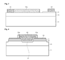
- Figure 4 is a cross-sectional view of a light emitting diode according to another exemplary embodiment of the present invention.
- Figure 5 is a plan view of a light emitting diode according to a further exemplary embodiment of the present invention.
- Figure 6 is a plan view of a light emitting diode according to yet another exemplary embodiment of the present invention.
- Figure 1 is a plan view of a light emitting diode according to an exemplary embodiment of the present invention
- Figure 2 is a cross-sectional view taken along line A-A of Figure 1
- Figure 3 is a cross-sectional view taken along line B-B of Figure 1 .
- the light emitting diode includes a substrate 21, a first conductive type semiconductor layer 23, an active layer 25, a second conductive type semiconductor layer 27, an insulation layer 31, first and second electrode pads 35, 33, and upper extensions 33a.
- the light emitting diode may further include connecting portions 33b, a transparent electrode layer 29, and lower extensions 35a.
- the substrate 11 may be a sapphire substrate, but is not limited thereto.
- the first conductive type semiconductor layer 23 is located on the substrate 21 1 and the second conductive type semiconductor layer 25 is located on the first conductive type semiconductor layer 27 with the active layer 25 interposed between the first and second conductive type semiconductor layers.
- the first conductive type semiconductor layer 23, active layer 25 and second conductive type semiconductor layer 27 may be formed of, but not limited to, a GaN-based compound semiconductor material such as (Al, In, Ga)N.
- the constituent elements and composition of the active layer 25 are determined to emit light having a required wavelength, for example, ultraviolet rays or blue light.
- the first conductive type semiconductor layer 23 may be an n-type nitride semiconductor layer and the second conductive type semiconductor layer 27 may be a p-type nitride semiconductor layer, or vice versa.
- the first conductive type semiconductor layer 23 and/or the second conductive type semiconductor layer 27 may have a single layer structure or a multilayer structure. Further, the active layer 25 may have a single quantum well structure or a multi-quantum well structure.
- the light emitting diode may further include a buffer layer (not shown) between the substrate 21 and the first conductive type semiconductor layer 23.
- These semiconductor layers 23, 25, 27 may be formed by a metal organic chemical vapor deposition (MOCVD) technique or molecular beam epitaxy (MBE) technique
- a transparent electrode layer 29 may be formed on the second conductive type semiconductor layer 27.
- the transparent electrode layer 29 may be formed of indium tin oxide (ITO) or Ni/Au and forms an ohmic contact with the second conductive type semiconductor layer.
- the second conductive type semiconductor layer 27 and the active layer 25 may be subjected to a process to expose a region(s) of the first conductive type semiconductor layer 23 via photolithography and etching.
- a process is generally known as a mesa-etching.
- the mesa etching may provide divided light emitting regions as shown in Figures 1 and 2 .
- the light emitting diode has two light emitting regions that are isolated from each other, the light emitting diode may have more than two separate light emitting regions.
- the mesa-etching may be performed to form inclined side surfaces which have a degree of inclination in the range of 30 ⁇ 70 degrees.
- the first and second electrode pads 35, 33 are located on the first conductive type semiconductor layer exposed through the mesa etching.
- the first electrode pad 35 is electrically connected to the first conductive type semiconductor layer 23.
- the second electrode pad 33 is insulated from the first conductive type semiconductor layer 23 by the insulation layer 31.
- the first and second electrode pads 35, 33 are bonding pads for bonding wires and have a relatively wide area for wire bonding.
- the first and second electrode pads 35, 33 may be formed on the exposed region(s) of the first conductive type semiconductor layer 23, but are not limited thereto.
- the insulation layer 31 is interposed between the second electrode pad 33 and the first conductive type semiconductor layer 23 to insulate the second electrode pad 33 from the first conductive type semiconductor layer 23. Further, the insulation layer 31 may cover the side surfaces of the second conductive type semiconductor layer 27 and the active layer 25, which are exposed by the mesa etching. The insulation layer 31 may extend to an upper surface of the second conductive type semiconductor layer 27 such that an edge of the insulation layer 31 1 overlaps the second conductive type semiconductor layer 27.
- the upper extensions 33a are located on the second conductive type semiconductor layer 27 (or transparent electrode layer 29).
- the upper extensions 33a may be connected to the second electrode pad 33 via connecting portions 33b, respectively, and may be electrically connected to the second conductive type semiconductor layer 27.
- the upper extensions 33a are disposed to allow uniform current spreading on the second conductive type semiconductor layer 27.
- the connecting portions 33b are separated from the side surfaces of the second conductive type semiconductor layer 27 and the active layer 25 by the insulation layer 31.
- At least one lower extension 35a may be extended from the first electrode pad 35.
- the lower extension 35a is located on the first conductive type semiconductor layer 23 and electrically connected thereto. As shown in the figures, the lower extension 35a may be located between the divided light emitting regions, but are not limited thereto. Alternatively, the lower extension 35a may be located outside the light emitting regions.
- the electrode pads 33, 35, the upper extensions 33a, the connecting portions 33b, and the lower extension 35a may be formed of, but are not limited to, the same material, for example, Cr/Au by the same process.
- the upper extensions 33a and the second electrode pad 33 may be formed of different materials by different processes.
- the divided light emitting regions have a symmetrical structure relative to a line, for example, a cut line B-B, which is located between the first electrode pad 35 and the second electrode pad 33.
- the upper extensions 33a are also disposed in a symmetrical structure, so that the light emitting regions may exhibit the same radiation characteristics. Accordingly, when a light emitting region is divided into two light emitting regions in a single light emitting diode, a process of packaging the light emitting diode may be further simplified than in the case of using two light emitting diodes connected in parallel to each other. Furthermore, the provision of the divided light emitting regions can relieve current crowding caused by defects and improve light extraction efficiency through formation of the inclined side surfaces by mesa etching.
- Figure 4 is a cross-sectional view of a light emitting diode according to another exemplary embodiment of the present invention.
- the light emitting diode of this embodiment is generally similar to the light emitting diode described with reference to Figures 1 to 3 .
- a portion of a second electrode pad 43 is located on a second conductive type semiconductor layer 27.
- the second electrode pad 43 is located on a first conductive type semiconductor layer 23 exposed through a mesa etching and a portion of the second electrode pad 43 is located on the second conductive type semiconductor layer 27.
- the second electrode pad 43 is isolated not only from the first conductive type semiconductor layer 23 but also from the second conductive type semiconductor layer 27 and the active layer 25 by an insulation layer 31. Extensions 33a are extended from the second electrode pad 43.
- the second electrode pad 43 is separated from the semiconductor layers by the insulation layer 31, thereby preventing current crowding around the second electrode pad 43. Furthermore, in this embodiment, an area subjected to mesa etching may be relatively decreased, thereby increasing the light emitting region.
- Figure 5 is a plan view of a light emitting diode according to a further exemplary embodiment of the present invention.
- the first and second electrode pads 35, 33 are disposed along a major axis of the light emitting diode, and the light emitting regions are divided from each other along the major axis of the light emitting diode.
- the light emitting diode according to this embodiment includes first and second electrode pads 53, 55 disposed along a minor axis of the light emitting diode and light emitting regions divided from each other along the minor axis of the light emitting diode. Further, the divided light emitting regions are disposed in a symmetrical structure and upper and lower extensions 53a, 55a are also disposed in a symmetrical structure.
- the upper extensions 53a extend along a periphery of the light emitting diode to surround the light emitting diode, and each of the upper extensions 55a has an extension 55b extending inward from the periphery of the light emitting diode.
- the lower extensions 55a extend from an inner side of the light emitting diode toward the outside of the light emitting diode.
- Each of the lower extensions 55a may be bifurcated to surround the extension 53b in each light emitting region.
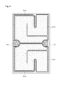
- Figure 6 is a plan view of a light emitting diode according to yet another exemplary embodiment of the present invention.
- the light emitting diode of this embodiment is generally similar to the light emitting diode described with reference to Figure 5 .
- lower extensions 65a and upper extensions 63a have distinctive arrangement.
- the lower extensions 65a extend along a periphery of the light emitting diode first and then extend into the light emitting regions, and each of the upper extensions 63a includes two extensions disposed on each of the light emitting regions, and these two extensions surround the lower extension 65a extending into the light emitting region.
- the light emitting diode is divided into two light emitting regions, but may be divided into more than two light emitting regions. In some embodiments, the light emitting regions may not be completely divided from each other. In other words, portions of the light emitting regions may be connected to each other.
Landscapes
- Led Devices (AREA)
Applications Claiming Priority (1)
| Application Number | Priority Date | Filing Date | Title |
|---|---|---|---|
| KR1020090123862A KR101055768B1 (ko) | 2009-12-14 | 2009-12-14 | 전극패드들을 갖는 발광 다이오드 |
Publications (2)
| Publication Number | Publication Date |
|---|---|
| EP2333849A2 true EP2333849A2 (de) | 2011-06-15 |
| EP2333849A3 EP2333849A3 (de) | 2013-05-08 |
Family
ID=43639128
Family Applications (1)
| Application Number | Title | Priority Date | Filing Date |
|---|---|---|---|
| EP10188092.0A Ceased EP2333849A3 (de) | 2009-12-14 | 2010-10-19 | Lichtemittierende Diode mit Elektroden-Pads |
Country Status (7)
| Country | Link |
|---|---|
| US (1) | US8541806B2 (de) |
| EP (1) | EP2333849A3 (de) |
| JP (2) | JP2011124580A (de) |
| KR (1) | KR101055768B1 (de) |
| CN (2) | CN102097566A (de) |
| TW (1) | TWI418061B (de) |
| WO (1) | WO2011074768A1 (de) |
Families Citing this family (39)
| Publication number | Priority date | Publication date | Assignee | Title |
|---|---|---|---|---|
| US9236532B2 (en) * | 2009-12-14 | 2016-01-12 | Seoul Viosys Co., Ltd. | Light emitting diode having electrode pads |
| WO2011083923A2 (en) | 2010-01-07 | 2011-07-14 | Seoul Opto Device Co., Ltd. | Light emitting diode having electrode pads |
| KR20120015651A (ko) * | 2010-08-12 | 2012-02-22 | 서울옵토디바이스주식회사 | 개선된 광 추출 효율을 갖는 발광 다이오드 |
| TW201320402A (zh) * | 2011-11-04 | 2013-05-16 | Lextar Electronics Corp | 固態發光半導體元件 |
| TWI479694B (zh) * | 2012-01-11 | 2015-04-01 | Formosa Epitaxy Inc | Light emitting diode wafers |
| KR101368720B1 (ko) | 2013-01-10 | 2014-03-03 | 주식회사 세미콘라이트 | 반도체 발광소자 |
| TWI438895B (zh) * | 2012-02-09 | 2014-05-21 | 隆達電子股份有限公司 | 發光二極體陣列 |
| TWI535077B (zh) | 2012-05-24 | 2016-05-21 | 台達電子工業股份有限公司 | 發光單元及其發光模組 |
| DE112013003931T5 (de) * | 2012-08-07 | 2015-06-03 | Seoul Viosys Co., Ltd. | Leuchtdiodenarray auf Wafer-Ebene und Verfahren zu dessen Herstellung |
| US10804316B2 (en) | 2012-08-07 | 2020-10-13 | Seoul Viosys Co., Ltd. | Wafer level light-emitting diode array |
| US9318529B2 (en) | 2012-09-07 | 2016-04-19 | Seoul Viosys Co., Ltd. | Wafer level light-emitting diode array |
| US10388690B2 (en) | 2012-08-07 | 2019-08-20 | Seoul Viosys Co., Ltd. | Wafer level light-emitting diode array |
| DE202013012470U1 (de) * | 2012-09-07 | 2017-01-12 | Seoul Viosys Co., Ltd. | Leuchtdiodenarray auf WAFER-Ebene |
| TWD154431S (zh) * | 2012-10-03 | 2013-07-01 | 晶元光電股份有限公司 | 發光二極體 |
| CN102881797B (zh) * | 2012-10-18 | 2015-02-25 | 安徽三安光电有限公司 | 具有电流扩展结构的氮化镓基发光二极管 |
| KR101532917B1 (ko) * | 2012-12-03 | 2015-07-01 | 일진엘이디(주) | 세퍼레이션 영역을 포함하여 전류 분산 효과가 우수한 고휘도 반도체 발광소자 |
| KR20140076204A (ko) * | 2012-12-12 | 2014-06-20 | 서울바이오시스 주식회사 | 발광다이오드 및 그 제조방법 |
| JP2014236038A (ja) * | 2013-05-31 | 2014-12-15 | 信越半導体株式会社 | 発光素子 |
| CN104425538B (zh) * | 2013-09-03 | 2019-05-03 | 晶元光电股份有限公司 | 具有多个发光结构的发光元件 |
| WO2015074353A1 (zh) * | 2013-11-25 | 2015-05-28 | 扬州中科半导体照明有限公司 | 一种半导体发光二极管芯片 |
| USD770397S1 (en) * | 2014-07-22 | 2016-11-01 | Epistar Corporation | Light-emitting diode unit |
| USD743355S1 (en) * | 2014-07-22 | 2015-11-17 | Epistar Corporation | Light-emitting diode unit |
| KR101888608B1 (ko) | 2014-10-17 | 2018-09-20 | 엘지이노텍 주식회사 | 발광 소자 패키지 및 조명 장치 |
| USD750580S1 (en) * | 2014-10-30 | 2016-03-01 | Epistar Corporation | Light-emitting diode array |
| US9905729B2 (en) | 2015-03-27 | 2018-02-27 | Seoul Viosys Co., Ltd. | Light emitting diode |
| USD775090S1 (en) * | 2015-04-23 | 2016-12-27 | Seoul Viosys Co., Ltd. | Light emitting diode |
| TWD178892S (zh) * | 2015-11-17 | 2016-10-11 | 晶元光電股份有限公司 | 發光二極體陣列之部分 |
| DE102017205639B4 (de) | 2016-04-18 | 2025-02-13 | Seoul Viosys Co., Ltd | Lumineszenzdiode mit hoher Effizienz |
| JP6928575B2 (ja) * | 2016-04-18 | 2021-09-01 | ソウル バイオシス カンパニー リミテッドSeoul Viosys Co.,Ltd. | 高効率発光ダイオード |
| KR102550007B1 (ko) * | 2016-11-30 | 2023-07-03 | 서울바이오시스 주식회사 | 복수의 발광셀들을 가지는 발광 다이오드 |
| US10475962B2 (en) * | 2017-02-15 | 2019-11-12 | Epistar Corporation | Optoelectronic device |
| CN106887490B (zh) * | 2017-02-21 | 2018-04-20 | 福建兆元光电有限公司 | 一种半导体led芯片 |
| CN106972090A (zh) * | 2017-04-14 | 2017-07-21 | 华南理工大学 | 一种弧线形n电极及垂直结构led芯片 |
| JP2018026597A (ja) * | 2017-11-16 | 2018-02-15 | ローム株式会社 | 発光素子および発光素子パッケージ |
| CN108198923A (zh) * | 2017-11-23 | 2018-06-22 | 华灿光电(浙江)有限公司 | 一种发光二极管芯片及其制作方法 |
| CN108110024A (zh) * | 2018-01-16 | 2018-06-01 | 福建兆元光电有限公司 | 一种半导体发光元件 |
| KR102590229B1 (ko) * | 2018-10-15 | 2023-10-17 | 삼성전자주식회사 | Led 소자 및 led 소자의 제조 방법 |
| WO2021077338A1 (zh) * | 2019-10-23 | 2021-04-29 | 安徽三安光电有限公司 | 发光二极管及其制作方法 |
| CN113659052B (zh) * | 2021-08-16 | 2023-08-01 | 泉州三安半导体科技有限公司 | 一种发光二极管、发光模块及显示装置 |
Citations (2)
| Publication number | Priority date | Publication date | Assignee | Title |
|---|---|---|---|---|
| US6650018B1 (en) | 2002-05-24 | 2003-11-18 | Axt, Inc. | High power, high luminous flux light emitting diode and method of making same |
| US20080210972A1 (en) * | 2007-01-03 | 2008-09-04 | Samsung Electro-Mechanics Co., Ltd. | Nitride-based semiconductor light emitting diode |
Family Cites Families (21)
| Publication number | Priority date | Publication date | Assignee | Title |
|---|---|---|---|---|
| JP3447527B2 (ja) * | 1996-09-09 | 2003-09-16 | 株式会社東芝 | 半導体発光素子およびその製造方法 |
| JP4810746B2 (ja) * | 2000-03-31 | 2011-11-09 | 豊田合成株式会社 | Iii族窒化物系化合物半導体素子 |
| JP4058937B2 (ja) * | 2001-11-07 | 2008-03-12 | 松下電器産業株式会社 | 半導体発光装置及びその製造方法 |
| JP4053926B2 (ja) * | 2002-05-27 | 2008-02-27 | 日亜化学工業株式会社 | 窒化物半導体発光素子とそれを用いた発光装置 |
| JP2005012091A (ja) * | 2003-06-20 | 2005-01-13 | Stanley Electric Co Ltd | 光ファイバ用ledおよびその製造方法 |
| CN2643486Y (zh) * | 2003-08-01 | 2004-09-22 | 艾笛森光电股份有限公司 | 半导体光源 |
| KR20060077801A (ko) * | 2004-12-31 | 2006-07-05 | 엘지전자 주식회사 | 고출력 발광 다이오드 및 그의 제조 방법 |
| TWI282866B (en) * | 2005-07-12 | 2007-06-21 | Benq Corp | Scan system with multi-light sources and method of the same |
| KR100616693B1 (ko) * | 2005-08-09 | 2006-08-28 | 삼성전기주식회사 | 질화물 반도체 발광 소자 |
| JP4978014B2 (ja) | 2006-01-30 | 2012-07-18 | サンケン電気株式会社 | 半導体発光装置及びその製造方法 |
| KR100833309B1 (ko) | 2006-04-04 | 2008-05-28 | 삼성전기주식회사 | 질화물계 반도체 발광소자 |
| KR100809220B1 (ko) | 2007-02-01 | 2008-02-29 | 삼성전기주식회사 | 반도체 발광소자 |
| CN102779918B (zh) * | 2007-02-01 | 2015-09-02 | 日亚化学工业株式会社 | 半导体发光元件 |
| TWI366291B (en) * | 2007-03-30 | 2012-06-11 | Epistar Corp | Semiconductor light-emitting device having stacked transparent electrodes |
| DE102007022947B4 (de) * | 2007-04-26 | 2022-05-05 | OSRAM Opto Semiconductors Gesellschaft mit beschränkter Haftung | Optoelektronischer Halbleiterkörper und Verfahren zur Herstellung eines solchen |
| JP2008283028A (ja) * | 2007-05-11 | 2008-11-20 | Fuji Xerox Co Ltd | 面発光型半導体レーザ、面発光型半導体レーザの製造方法、モジュール、光源装置、情報処理装置、光送信装置、光空間伝送装置および光空間伝送システム。 |
| JP5178360B2 (ja) * | 2007-09-14 | 2013-04-10 | シャープ株式会社 | 窒化物半導体発光素子 |
| TW200919768A (en) * | 2007-10-19 | 2009-05-01 | Huga Optotech Inc | Semiconductor light-emitting device and method of fabricating the same |
| CN101257072B (zh) * | 2007-12-26 | 2010-12-15 | 厦门市三安光电科技有限公司 | 一种立体式空间分布电极的发光二极管及其制造方法 |
| CN101499510B (zh) | 2008-01-30 | 2011-06-22 | 富士迈半导体精密工业(上海)有限公司 | 半导体发光元件 |
| JP5148336B2 (ja) * | 2008-03-26 | 2013-02-20 | 京セラ株式会社 | 発光ダイオードチップおよびその製造方法 |
-
2009
- 2009-12-14 KR KR1020090123862A patent/KR101055768B1/ko active Active
-
2010
- 2010-10-12 WO PCT/KR2010/006960 patent/WO2011074768A1/en not_active Ceased
- 2010-10-19 EP EP10188092.0A patent/EP2333849A3/de not_active Ceased
- 2010-11-16 CN CN2010105516780A patent/CN102097566A/zh active Pending
- 2010-11-16 CN CN201510823096.6A patent/CN105489728B/zh active Active
- 2010-11-23 TW TW099140424A patent/TWI418061B/zh active
- 2010-12-09 US US12/963,921 patent/US8541806B2/en active Active
- 2010-12-10 JP JP2010275336A patent/JP2011124580A/ja active Pending
-
2015
- 2015-05-07 JP JP2015095055A patent/JP6199338B2/ja active Active
Patent Citations (2)
| Publication number | Priority date | Publication date | Assignee | Title |
|---|---|---|---|---|
| US6650018B1 (en) | 2002-05-24 | 2003-11-18 | Axt, Inc. | High power, high luminous flux light emitting diode and method of making same |
| US20080210972A1 (en) * | 2007-01-03 | 2008-09-04 | Samsung Electro-Mechanics Co., Ltd. | Nitride-based semiconductor light emitting diode |
Also Published As
| Publication number | Publication date |
|---|---|
| KR20110067313A (ko) | 2011-06-22 |
| WO2011074768A1 (en) | 2011-06-23 |
| TW201138152A (en) | 2011-11-01 |
| US8541806B2 (en) | 2013-09-24 |
| JP6199338B2 (ja) | 2017-09-20 |
| JP2011124580A (ja) | 2011-06-23 |
| JP2015159328A (ja) | 2015-09-03 |
| KR101055768B1 (ko) | 2011-08-11 |
| EP2333849A3 (de) | 2013-05-08 |
| US20110140160A1 (en) | 2011-06-16 |
| CN105489728B (zh) | 2018-11-16 |
| TWI418061B (zh) | 2013-12-01 |
| CN102097566A (zh) | 2011-06-15 |
| CN105489728A (zh) | 2016-04-13 |
Similar Documents
| Publication | Publication Date | Title |
|---|---|---|
| US8541806B2 (en) | Light emitting diode having electrode pads | |
| US9793440B2 (en) | Light emitting diode having electrode pads | |
| US8525212B2 (en) | Light emitting diode having electrode extensions | |
| US9397264B2 (en) | Light emitting diode chip having electrode pad | |
| US9673355B2 (en) | Light emitting diode having electrode pads | |
| US8680559B2 (en) | Light emitting diode having electrode extensions for current spreading | |
| US20130134867A1 (en) | Light emitting diode with improved light extraction efficiency | |
| KR101636034B1 (ko) | 전극패드들을 갖는 발광 다이오드 | |
| KR20110083968A (ko) | 전극패드들을 갖는 발광 다이오드 | |
| KR20110084591A (ko) | 전극패드들을 갖는 발광 다이오드 | |
| KR101623950B1 (ko) | 전극패드들을 갖는 발광 다이오드 | |
| KR101615277B1 (ko) | 전극패드들을 갖는 발광 다이오드 | |
| KR101618800B1 (ko) | 전극패드들을 갖는 발광 다이오드 | |
| KR101618799B1 (ko) | 전극패드들을 갖는 발광 다이오드 | |
| KR101615283B1 (ko) | 전극패드들을 갖는 발광 다이오드 |
Legal Events
| Date | Code | Title | Description |
|---|---|---|---|
| PUAI | Public reference made under article 153(3) epc to a published international application that has entered the european phase |
Free format text: ORIGINAL CODE: 0009012 |
|
| 17P | Request for examination filed |
Effective date: 20101019 |
|
| AK | Designated contracting states |
Kind code of ref document: A2 Designated state(s): AL AT BE BG CH CY CZ DE DK EE ES FI FR GB GR HR HU IE IS IT LI LT LU LV MC MK MT NL NO PL PT RO RS SE SI SK SM TR |
|
| AX | Request for extension of the european patent |
Extension state: BA ME |
|
| RAP1 | Party data changed (applicant data changed or rights of an application transferred) |
Owner name: SEOUL OPTO DEVICE CO., LTD. |
|
| PUAL | Search report despatched |
Free format text: ORIGINAL CODE: 0009013 |
|
| AK | Designated contracting states |
Kind code of ref document: A3 Designated state(s): AL AT BE BG CH CY CZ DE DK EE ES FI FR GB GR HR HU IE IS IT LI LT LU LV MC MK MT NL NO PL PT RO RS SE SI SK SM TR |
|
| AX | Request for extension of the european patent |
Extension state: BA ME |
|
| RIC1 | Information provided on ipc code assigned before grant |
Ipc: H01L 33/38 20100101AFI20130404BHEP Ipc: H01L 33/44 20100101ALN20130404BHEP |
|
| RAP1 | Party data changed (applicant data changed or rights of an application transferred) |
Owner name: SEOUL VIOSYS CO., LTD |
|
| 17Q | First examination report despatched |
Effective date: 20160502 |
|
| STAA | Information on the status of an ep patent application or granted ep patent |
Free format text: STATUS: THE APPLICATION HAS BEEN REFUSED |
|
| 18R | Application refused |
Effective date: 20181105 |