EP2330594A1 - Nichtflüchtige logische Vorrichtungen mit Magnettunnelübergängen - Google Patents
Nichtflüchtige logische Vorrichtungen mit Magnettunnelübergängen Download PDFInfo
- Publication number
- EP2330594A1 EP2330594A1 EP10290278A EP10290278A EP2330594A1 EP 2330594 A1 EP2330594 A1 EP 2330594A1 EP 10290278 A EP10290278 A EP 10290278A EP 10290278 A EP10290278 A EP 10290278A EP 2330594 A1 EP2330594 A1 EP 2330594A1
- Authority
- EP
- European Patent Office
- Prior art keywords
- magnetic tunnel
- register
- inverter
- register cell
- shift
- Prior art date
- Legal status (The legal status is an assumption and is not a legal conclusion. Google has not performed a legal analysis and makes no representation as to the accuracy of the status listed.)
- Granted
Links
- 230000005291 magnetic effect Effects 0.000 title claims abstract description 112
- 230000005415 magnetization Effects 0.000 claims description 16
- 238000010438 heat treatment Methods 0.000 claims description 13
- 238000000034 method Methods 0.000 claims description 12
- 230000002457 bidirectional effect Effects 0.000 claims description 7
- 238000000262 chemical ionisation mass spectrometry Methods 0.000 claims 1
- 230000015654 memory Effects 0.000 description 18
- 238000005516 engineering process Methods 0.000 description 12
- 230000010354 integration Effects 0.000 description 4
- 238000012545 processing Methods 0.000 description 4
- 230000008901 benefit Effects 0.000 description 3
- 238000013461 design Methods 0.000 description 3
- 238000010586 diagram Methods 0.000 description 3
- 230000010287 polarization Effects 0.000 description 3
- 230000000295 complement effect Effects 0.000 description 2
- 238000013500 data storage Methods 0.000 description 2
- 230000002829 reductive effect Effects 0.000 description 2
- 101100298835 Saccharomyces cerevisiae (strain ATCC 204508 / S288c) RPT1 gene Proteins 0.000 description 1
- 230000003466 anti-cipated effect Effects 0.000 description 1
- 230000005290 antiferromagnetic effect Effects 0.000 description 1
- 230000000903 blocking effect Effects 0.000 description 1
- 239000000872 buffer Substances 0.000 description 1
- 238000004364 calculation method Methods 0.000 description 1
- 239000000969 carrier Substances 0.000 description 1
- 238000007796 conventional method Methods 0.000 description 1
- 238000001816 cooling Methods 0.000 description 1
- 230000003247 decreasing effect Effects 0.000 description 1
- 238000011161 development Methods 0.000 description 1
- 230000018109 developmental process Effects 0.000 description 1
- 230000000694 effects Effects 0.000 description 1
- 230000000670 limiting effect Effects 0.000 description 1
- 230000002093 peripheral effect Effects 0.000 description 1
- 230000003252 repetitive effect Effects 0.000 description 1
- 230000008672 reprogramming Effects 0.000 description 1
- 238000012827 research and development Methods 0.000 description 1
- 230000002441 reversible effect Effects 0.000 description 1
- 230000003068 static effect Effects 0.000 description 1
- 238000012546 transfer Methods 0.000 description 1
Images


Classifications
-
- G—PHYSICS
- G11—INFORMATION STORAGE
- G11C—STATIC STORES
- G11C19/00—Digital stores in which the information is moved stepwise, e.g. shift registers
- G11C19/02—Digital stores in which the information is moved stepwise, e.g. shift registers using magnetic elements
- G11C19/08—Digital stores in which the information is moved stepwise, e.g. shift registers using magnetic elements using thin films in plane structure
-
- G—PHYSICS
- G11—INFORMATION STORAGE
- G11C—STATIC STORES
- G11C11/00—Digital stores characterised by the use of particular electric or magnetic storage elements; Storage elements therefor
- G11C11/02—Digital stores characterised by the use of particular electric or magnetic storage elements; Storage elements therefor using magnetic elements
- G11C11/16—Digital stores characterised by the use of particular electric or magnetic storage elements; Storage elements therefor using magnetic elements using elements in which the storage effect is based on magnetic spin effect
- G11C11/165—Auxiliary circuits
- G11C11/1675—Writing or programming circuits or methods
-
- G—PHYSICS
- G11—INFORMATION STORAGE
- G11C—STATIC STORES
- G11C14/00—Digital stores characterised by arrangements of cells having volatile and non-volatile storage properties for back-up when the power is down
- G11C14/0054—Digital stores characterised by arrangements of cells having volatile and non-volatile storage properties for back-up when the power is down in which the volatile element is a SRAM cell
- G11C14/0081—Digital stores characterised by arrangements of cells having volatile and non-volatile storage properties for back-up when the power is down in which the volatile element is a SRAM cell and the nonvolatile element is a magnetic RAM [MRAM] element or ferromagnetic cell
-
- G—PHYSICS
- G11—INFORMATION STORAGE
- G11C—STATIC STORES
- G11C19/00—Digital stores in which the information is moved stepwise, e.g. shift registers
- G11C19/02—Digital stores in which the information is moved stepwise, e.g. shift registers using magnetic elements
-
- G—PHYSICS
- G11—INFORMATION STORAGE
- G11C—STATIC STORES
- G11C8/00—Arrangements for selecting an address in a digital store
- G11C8/04—Arrangements for selecting an address in a digital store using a sequential addressing device, e.g. shift register, counter
Definitions
- the present disclosure generally relates to program registers and a programmable logic circuit, such as flip-flops, shift registers and the like.
- the present disclosure relates more specifically to a technology for storing data or performing a logic operation on the program registers.
- Embedded SRAMs is one of the most frequently used memory embedded in logic chips, and typical applications include on-chips buffers, caches, register files, and so on.
- the small access time makes it popular in the logic lCs industry. Nonetheless, its volatility and the need of an external nonvolatile memory to store the configuration data make it not suitable for nowadays embedded applications.
- the use of a nonvolatile internal memory like flash technology allows the chip to be powered down in the standby mode when not in use in order to reduce power consumption.
- these FPGAs use flash memory in there configuration layer which makes it ready to run at power up.
- clock gating in which the circuit clock is stopped when arithmetic processing is not being performed
- power gating in which power is shut down to circuits not performing operational processing.
- clock gating it is not possible to stop leakage current in the circuit, reducing the power-saving effects
- power gating although most of the leakage current can be stopped by shutting off power, it cannot be completely eliminated due to the need for power to be supplied to the register.
- power can but shut off to the circuit, including for the register, making it possible to reduce power consumption to zero.
- nv-SRAM nonvolatile non-volatile
- type flash non-volatile components
- Flash writing/erasing voltages of Flash are high and not very compatible with supply voltages of SRAM cells, which impose additional devices.
- these technologies have a low endurance ( ⁇ 1E10) and they are poorly suited for applications such as cache memory (embedded memory in logic ICs devices) and can ensure a fair backup at very low frequencies.
- Non-volatile registers are a data storage circuits which retain stored information in the absence of power.
- digital processing (logic) circuits the storage area used to temporarily retain mid-calculation data, arithmetic processing, or operational status is called a register.
- registers are dispersed within the logic circuit.
- Logic ICs i.e. CPUs
- FPGA Field Programmable Gate array
- Conventional logic ICs are volatile, meaning shutting off power to the IC will cause information in the register to be lost. Therefore, power must constantly be supplied to the IC.
- Register include a plurality of register cells 1, each of which has input D, a clock input CK, data output Q and inverse data QN.
- the present application discloses a register cell which overcome at least some limitations of the prior art.
- a register cell can comprise a differential amplifying portion containing a first inverter coupled to a second inverter such as to form an unbalanced flip-flop circuit; a first and second bit line connected to one end of the first and second inverter, respectively; and a first and second source line connected to the other end of the first and second inverter, respectively; characterized by the register cell further comprising a first and second magnetic tunnel junction electrically connected to the other end of the first and second inverter, respectively.
- said first inverter comprises a first PMOS transistor connected in series with a NMUS transistor and the second inverter comprises a second PMOS transistor connected in series with a second NMOS transistor.
- one end of the first and second magnetic tunnel junction is connected to the first NMOS transistor and to the drain of the second NMOS transistor, respectively.
- the first and second magnetic funnel junction are connected, respectively, between the drain of the first PMOS and NMOS transistors and the drain of the second PMOS and NMOS transistors.
- the first and second magnetic tunnel junction are arranged to have opposite resistance values.
- the present disclosure also concerns a shift register which overcome at least some limitations of the prior art, wherein the shift register can comprise a plurality of the register cells; each register cell being connected in series to the adjacent register cell via a shift transistor used to chain together the two inverters of the adjacent register cells and to shift data from one node of one register cell to one node of the adjacent register cell.
- the shift register further comprises a clock line adapted to generate clock signal such as to shift a data stored in the second inverter of one of the register cells to the first inverter of the first inverter of the adjacent successive register cell, during a shift operation.
- the present disclosure also pertains to a method for writing the shift register comprising:
- said heating comprises passing a heating current through the selected magnetic tunnel junctions using the stored data in the adjacent register cell.
- the shift register further comprise a field line arranged such that an external magnetic field generated by a field current passing in the field line can address simultaneously all magnetic tunnel junctions of the register cells, and said changing the magnetic state comprises passing the field current in the field line.
- said changing the magnetic state comprises passing a CIMS current through the selected magnetic tunnel junctions.
- the register cell and shift register disclosed herein can be made smaller than conventional shift registers and power consumption during the write and read operation of the shift registers can be low.
- the use of nonvolatile memories such as magnetic tunnel junctions helps to overcome the drawbacks of classical SRAM-based logic ICs without significant speed penalty, Besides its advantage that lies in power saving during the standby mode, it also benefits to the configuration time reduction since there is no need to load the configuration data from an external nonvolatile memory as used in SRAM based logic ICs.
- the magnetic tunnel junctions-based shift register can be written which allows a dynamic (or shadowed) configuration and further increases the flexibility of Logic ICs circuit.
- register cell and shift register disclosed herein have high-timing performance, allow for high-density integration, reliable data storage, good endurance, and low number of additional masks for the magnetic post-process since the integration of shift register is made by an "above- IC" technology.
- Fig. 2 illustrates a non-volatile unbalanced register cell 1 according to an embodiment.
- the register cell 1 comprises cross coupled first and second inverter 3, 3' forming an unbalanced flip-flop circuit.
- the first and second inverters 3, 3' comprise respectively a first PMOS transistor P1 connected in series with a NMOS transistor N1, and a second PMOS transistor P2 connected in series with a second NMOS transistor N2.
- the gates of the first transistors P1 and N1 are coupled to the drain of the second transistors P2 and source of the second transistors N2, respectively.
- the sources of the first and second transistors P1 and P2 and connected to a first bit line B 1.0 and a second bit line By, respectively.
- a first and a second magnetic tunnel junction are connected at one end respectively to the first inverter 3, via the drain of the first NMOS transistor N1 (represented as node 4 in Fig.2 ), and to the second inverter 3', via the drain of the second NMOS transistor N2 (represented as node 4' in Fig.2 ).
- the two magnetic tunnel junctions 6, 6' can be arranged to have opposite resistance values, for example a maximum and a minimum resistance value, respectively, coding one logic bit.
- the two inverters 3, 3' act as a 1-bit analog to digital converter (ADC), converting the differential resistance, or the difference between the first and second resistance of the first and second magnetic tunnel junction 6, 6', to a so call rail-to-rail voltage (binary information).
- a first source line S L0 and a second source line S L1 connect the other side of the first and second inverters 3, 3' to the drain of the first and second NMOS transistor sN1, N2, respectively, via the other end of the first and a second magnetic tunnel junction 6, 6', respectively.
- the magnetic tunnel junction 6, 6' can be formed from a reference layer having a fixed magnetization, a storage layer having a magnetization direction that can be switched from a first stable direction to a second stable direction upon writing of the cell, and an insulating layer between the storage layer and the sense layer.
- the magnetic state of the magnetic tunnel junction 6, 6' is defined by the relative orientation of the reference and storage layer magnetization.
- the register cell 1 Upon start-up of the register cell 1, a voltage is applied to the first and second bit line B L0 , B L1 (signals go high) and, depending on the resistance values of the first and second magnetic tunnel junctions 6, 6', an intput of the first inverter 3, represented by the node Q in Fig. 2 , is pulled high (V DD ), while an output of the second inverter 3', represented by the node Qn in Fig. 2 , is pulled down (0 V).
- the register cell 1 is formed from a differential amplifying portion 2, or CMOS volatile stage, comprising the two inverters 3, 3', and a magnetic nonvolatile stage portion, comprising the two magnetic tunnel junctions 6, 6'. In this configuration, the register cell 1 allows for a dial storage volatile and nonvolatile facility.
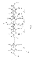
- FIG. 3 a block/schematic diagram of a non-volatile magnetic shift register 10 is illustrated according to an embodiment.
- the shift register 10 includes a plurality of the register cells 1 according to the embodiment of Fig. 2 .
- the succession of register cells 1 is indicated by the symbol "n-i", with the first and last register cells 1 of the shift register 10 being indicated by the symbols "0" and "n-1 ", respectively.
- Each register cell 1 of the magnetic shift register 10 is connected in series to an adjacent register cell 1, via a shift transistor 11.
- the shift transistor 11 is used to chain together the two inverters 3, 3' of the adjacent register cells 1 and to shift data from one of the input and output nodes Q, Qn of one of the register cells 1 to the one of the input and output nodes Q, Qn of the adjacent register cell 1.
- a clock line is adapted to generate clock signal comprising repetitive alternating ones and zeros or continuous alternating square wave.
- the side of the second bit line BL1 of one of the cell registers 1, for example "n-3”, is at V DD and the side of the first bit line B L0 of the adjacent cell register 1, "n-2", is at 0V.
- the clock signal generated by the clock line CK has a value corresponding to one, the data stored in the second inverter 3' and outputted at the output node Qn is shifted through the shift transistor 11 to the first inverter 3 of the adjacent register cell 1, via its input Q.
- bits of information are applied serially to a data input, shown by node 12 in Fig. 3 , of the first register cell 1.
- the data is then clocked to the first register cell 1, "0", by the clock signal generated by the clock line CK applied simultaneously to the input Q of all cell registers 1, via the gate of the respective shift transistor 11.
- the symbol CK represents "not CK", or the clock lines CK applying a clock signal inverse of the clock signal applied by the clock lines CK,
- the other bits stored in the subsequent cell registers 1 are simultaneously clocked into the next adjacent cell register 1 or clocked out of last register 1 ("n-1") via its data output 13.
- Fig. 4a to c illustrates schematically a writing operation of the non-volatile shift register 10 for a singe memory register cell 1, according to an embodiment. More particularly, the writing operation is based on a thermally assisted switching (TAS) -based writing operation where the magnetic tunnel junction 6, 6' is heated at a predetermined high threshold temperature in order to switch the magnetization of the storage layer.
- TAS thermally assisted switching
- magnetic tunnel junctions 6, 6' having the same magnetic state in the shift register 10 are selected by shifting an information sequence data such as to have a high voltage V DD at the corresponding input and/or output Q, Qn, of the register cells 1.
- the same magnetic state means a low resistance value, where the magnetizations of the storage and reference layers are parallel, or a high resistance value where the magnetizations of the storage and reference layers are antiparallel.
- FIG. 4a An exemplary first writing step of the writing operation is represented in Fig. 4a for one of the register cell 1 having a selected first magnetic tunnel junction 6.
- the first magnetic tunnel junction 6 is heated by passing a heating current 31 by using the stored data in the register cell 1. More particularly, when the voltage V DD is applied at the input Q, the signal of the first source line S L0 goes low (VL) such as to have enough voltage across the first transistor N1 and the magnetic tunnel junction 6 such that the heating current 31 passing through the magnetic tunnel junction 6 is high enough to heat the magnetic tunnel junction 6 to the predetermined high threshold temperature.
- the heating current pulse 31 is controlled via the first source line S L0 .
- the high threshold temperature can corresponds to a blocking temperature of about 150°C of an antiferromagnetic layer (not shown) pinning the storage layer.
- an external magnetic field is applied to the magnetic tunnel junction 6 such as to change switch the magnetization direction of the storage layer.
- the external magnetic field is generated by passing a field current through a field line arranged such as the generated external magnetic field can address simultaneously all of the selected magnetic tunnel junctions 6, 6 and switch the magnetization of their storage layer in a direction according the external magnetic field.
- the external magnetic field must be higher than the coercitivity of the storage layer to switch its magnetization direction.
- the shared field line perform a low power writing operation since a two step current pulse is used to write all magnetic tunnel junctions 6, 6'. Performing the writing operation with the two step current pulse means that a low and high resistance value is sequentially written in the magnetic tunnel junctions 6, 6'.
- the heating current 31 is then turned off in order to cool the magnetic tunnel junction 6 at a low threshold temperature to freeze the magnetization of the storage layer in the written state. Turning off the heating current 31 is performed by setting the first selection source line S L0 , in a high level mode (VH). The field current can maintained during the cooling of the magnetic tunnel junctions 6 and then switched off, once the magnetic tunnel junction 6 have reached the low threshold temperature. After completing the first writing step, the resistance of the first magnetic tunnel junction 6 is changed from a low to a high value, or a high to a low value, depending on the relative orientation of the storage layer and reference layer magnetizations, prior and after the first writing step.
- a third writing step shown in Fig. 4c the second magnetic tunnel junctions 6' is written in a complementary way after the shift register 10 has been clocked in the second step.
- the expression written in a complementary way means that the second magnetic tunnel junciton6' is written such as to have its resistance value opposite to the one of the first magnetic tunnel junction 6.
- the writing operation is the same as the one described in the first step.
- the field current is passed in the field line with a polarity opposite to the one during the writing operation in the first step.
- the bit lines BL0, BL1 are set at a high voltage V DD and the register cell 1 pre-amplifies locally the data stored magnetically in the two magnetic tunnel junctions 6, 6'.
- the data can then be read at the input Q, or output Qn, of the register cell 1 by shifting until the data output the node Qn for the read operation.
- the read operation allows for reading data bit by bit, or by block of bits, depending of the read circuit at the end of shift register 10.
- Fig. 5 represents the non-volatile register cell 1 in another embodiment.
- the first and second magnetic tunnel junctions 6, 6' are disposed, respectively, between the drain of the first PMOS and NMOS transistors P1, N1, and the drain of the second PMOS and NMOS transistors P2, N2.
- the register cell 1 can be connected in series to other identical register cells 1 in order to form the non-volatile shift register 10, as described above. The start-up and the writing operation can be performed as described above.
- the writing operation of the register cell 1 can also be performed by using a spin polarized (STT) current or by using an induced magnetic switching (C1MS) current, instead of the field current.
- STT spin polarized
- C1MS induced magnetic switching
- the STT or CIMS current can also be combined with the TAS.
- the writing operation of the register cell 1 is performed by using an induced magnetic switching (CIMS) current in combination with the TAS.
- CIMS induced magnetic switching
- the writing operation is similar to the one describe above in the embodiment of Figs. 4a to 4c , but no external magnetic field is used.
- the CIMS current pulse 32 is passed through the magnetic tunnel junction 6, 6' to change its magnetic state in accordance with the ClMS current polarization.
- the CIMS current 32 is passed through the magnetic tunnel junction 6, 6' being heated at the predetermined high threshold temperature.
- the CIMS current 32 can be appropriately spin-polarized by adding one or several specific magnetic layers, for example, magnetic layers having a perpendicular magnetization in the magnetic tunnel junction 6, 6', as described in patent US6603677 .
- Performing the writing operation using the STT or CIMS currents is highly scalable since the STT or CIM5 currents scales with the area of the magnetic tunnel junction 6, 6'. Furthermore, the writing operation using the STT or CIMS currents is potentially very fast and the register cell 1 does not require the additional field line to generate the external magnetic field, hence reducing both the size of the register cell 1 and the corresponding driver overhead. Moreover, the CIMS-based writing operation combined with the TAS allows for reduced write power consumption, particularly with small feature sizes. The readout remains similar to the one in the magnetic field-driven shift register architecture.
- Fig. 6 shows the shift register 10 comprising a plurality of the register cells 1 according to the embodiment of Fig. 5 . More particularly, three adjacent register cells 1 successively indicated by the symbols "I-1", “I” and “I+1 " are represented in Fig. 6 . The adjacent register cells 1 are arranged such that a bidirectional current I SW flows through all magnetic tunnel junctions 6, 6'.
- the bidirectional current I SW is made to flow from the node V S1 to the node V S0 by pulling up the node V S1 to a high value and by pulsing down the node V S0 to ground.
- This enables writing the shift register 10 by changing the magnetic state of the second magnetic tunnel junctions 6' of the register cell 1 indicated by "I-1", for example, by switching the magnetization of the storage layer to a direction parallel or antiparallel of that of the reference layer.
- the register cell 1 "I” stores a value "0" at its input Q and a value V DD at its output Qn and the register cell 1 "I-1” stores a value V DD at its input Q and a value "0” at its output Qn.
- passing the bidirectional current I SW in the opposite direction is performed by inversing the polarization of V S0 and V S1 , and by shifting the information by one clock cycle.
- the second magnetic tunnel junction 6' can be written in the same manner by passing the bidirectional current I SW through it, and changing the polarization of the bit lines V B0 and V B1 .
- the shift register 10 disclosed herein comprises only five transistors N1, N2, P1, P2, 11 per register cell 1.
- the four transistors N1, N2, P1, P2 being used for the register cell 1 and to convert the analog resistance variation of the two magnetic tunnel junctions 6, 6' to a rail-to-rail data at the output Qn of the register cell 1.
- the fifth transistor, or shift transistor 11, is used to shift data from one of the register cells 1 to the adjacent register cell 1. Since the transistors N1, N2, P1, P2, 11 can be small, indeed, the smallest size for a given technology can be used, power consumption during the write and read operation can be low. Moreover, the surface area of the shift register 10 can also be small.
- the shift register 10 according to the embodiment can also be used as a hybrid register cell. More particularly, since the magnetic tunnel junctions 6, 6' are integrated directly on circuits, a type of integration commonly known as "above IC", they can be optionally implemented on the shift register 10 using extra magnetic masks. Consequently, the non-volatile magnetic elements, or the two magnetic tunnel junctions 6, 6', can be added to a standard shift register in a same process flow to obtain the shift register 10 according to the above embodiments.
Landscapes
- Engineering & Computer Science (AREA)
- Microelectronics & Electronic Packaging (AREA)
- Computer Hardware Design (AREA)
- Static Random-Access Memory (AREA)
- Mram Or Spin Memory Techniques (AREA)
- Shift Register Type Memory (AREA)
- Hall/Mr Elements (AREA)
- Logic Circuits (AREA)
Priority Applications (1)
| Application Number | Priority Date | Filing Date | Title |
|---|---|---|---|
| EP10290278.0A EP2330594B1 (de) | 2009-05-26 | 2010-05-26 | Nichtflüchtige logische Vorrichtungen mit Magnettunnelübergängen |
Applications Claiming Priority (2)
| Application Number | Priority Date | Filing Date | Title |
|---|---|---|---|
| EP09290387 | 2009-05-26 | ||
| EP10290278.0A EP2330594B1 (de) | 2009-05-26 | 2010-05-26 | Nichtflüchtige logische Vorrichtungen mit Magnettunnelübergängen |
Publications (2)
| Publication Number | Publication Date |
|---|---|
| EP2330594A1 true EP2330594A1 (de) | 2011-06-08 |
| EP2330594B1 EP2330594B1 (de) | 2018-07-11 |
Family
ID=43220032
Family Applications (1)
| Application Number | Title | Priority Date | Filing Date |
|---|---|---|---|
| EP10290278.0A Active EP2330594B1 (de) | 2009-05-26 | 2010-05-26 | Nichtflüchtige logische Vorrichtungen mit Magnettunnelübergängen |
Country Status (3)
| Country | Link |
|---|---|
| US (1) | US8218349B2 (de) |
| EP (1) | EP2330594B1 (de) |
| JP (1) | JP5200060B2 (de) |
Families Citing this family (14)
| Publication number | Priority date | Publication date | Assignee | Title |
|---|---|---|---|---|
| JP5946683B2 (ja) | 2011-04-22 | 2016-07-06 | 株式会社半導体エネルギー研究所 | 半導体装置 |
| JP5814680B2 (ja) * | 2011-07-29 | 2015-11-17 | 株式会社東芝 | 磁気抵抗素子及び磁気メモリ |
| WO2013047213A1 (ja) * | 2011-09-27 | 2013-04-04 | 日本電気株式会社 | 不揮発抵抗ネットワーク集合体、および、それを用いた障害耐性を高めた不揮発論理ゲート |
| KR102149882B1 (ko) * | 2012-01-01 | 2020-08-31 | 고쿠리츠다이가쿠호진 도호쿠다이가쿠 | 집적회로 |
| US8933750B2 (en) | 2012-02-17 | 2015-01-13 | Crocus Technology Inc. | Magnetic logic units configured as an amplifier |
| US8913422B2 (en) | 2012-09-28 | 2014-12-16 | Intel Corporation | Decreased switching current in spin-transfer torque memory |
| JP6148534B2 (ja) * | 2013-05-20 | 2017-06-14 | 株式会社東芝 | 不揮発性メモリ |
| WO2015187877A1 (en) | 2014-06-06 | 2015-12-10 | Crocus Technology Inc. | Serial magnetic logic unit architecture |
| TWI753908B (zh) * | 2016-05-20 | 2022-02-01 | 日商半導體能源硏究所股份有限公司 | 半導體裝置、顯示裝置及電子裝置 |
| US9870811B2 (en) * | 2016-06-17 | 2018-01-16 | Qualcomm Incorporated | Physically unclonable function based on comparison of MTJ resistances |
| US10424380B1 (en) * | 2018-06-15 | 2019-09-24 | Qualcomm Incorporated | Physically unclonable function (PUF) memory employing static random access memory (SRAM) bit cells with added passive resistance to enhance transistor imbalance for improved PUF output reproducibility |
| US10803942B1 (en) | 2019-06-07 | 2020-10-13 | Qualcomm Technologies, Inc. | Transistor noise tolerant, non-volatile (NV) resistance element-based static random access memory (SRAM) physically unclonable function (PUF) circuits, and related systems and methods |
| CN112863575B (zh) * | 2019-11-12 | 2023-12-29 | 上海磁宇信息科技有限公司 | 具有磁性隧道结的非易失寄存器 |
| CN112927737B (zh) * | 2019-12-05 | 2024-01-05 | 上海磁宇信息科技有限公司 | 使用磁性隧道结的非易失寄存器 |
Citations (6)
| Publication number | Priority date | Publication date | Assignee | Title |
|---|---|---|---|---|
| US5695864A (en) | 1995-09-28 | 1997-12-09 | International Business Machines Corporation | Electronic device using magnetic components |
| US20020101761A1 (en) * | 2001-01-31 | 2002-08-01 | Motorola, Inc. | Non-volatile magnetic register |
| US6603677B2 (en) | 2000-12-07 | 2003-08-05 | Commissariat A L'energie Atomique | Three-layered stacked magnetic spin polarization device with memory |
| US6950335B2 (en) | 2001-11-16 | 2005-09-27 | Commissariat A L'energie Atomique | Magnetic tunnel junction magnetic device, memory and writing and reading methods using said device |
| US7474574B1 (en) * | 2007-07-02 | 2009-01-06 | International Business Machines Corporation | Shift register latch with embedded dynamic random access memory scan only cell |
| US20100110744A1 (en) * | 2008-11-04 | 2010-05-06 | Crocus Technology Sa | Ternary content addressable magnetoresistive random access memory cell |
Family Cites Families (15)
| Publication number | Priority date | Publication date | Assignee | Title |
|---|---|---|---|---|
| US6191973B1 (en) * | 1999-09-27 | 2001-02-20 | Motorola Inc. | Mram cam |
| US6178111B1 (en) * | 1999-12-07 | 2001-01-23 | Honeywell Inc. | Method and apparatus for writing data states to non-volatile storage devices |
| US6560146B2 (en) * | 2001-09-17 | 2003-05-06 | Sandisk Corporation | Dynamic column block selection |
| JP3834787B2 (ja) * | 2001-11-22 | 2006-10-18 | インターナショナル・ビジネス・マシーンズ・コーポレーション | 不揮発性ラッチ回路 |
| JP3864248B2 (ja) * | 2001-12-17 | 2006-12-27 | インターナショナル・ビジネス・マシーンズ・コーポレーション | 半導体装置 |
| JP3768504B2 (ja) * | 2002-04-10 | 2006-04-19 | 松下電器産業株式会社 | 不揮発性フリップフロップ |
| US6667897B1 (en) * | 2002-06-28 | 2003-12-23 | International Business Machines Corporation | Magnetic tunnel junction containing a ferrimagnetic layer and anti-parallel layer |
| JP4133149B2 (ja) * | 2002-09-12 | 2008-08-13 | 株式会社ルネサステクノロジ | 半導体記憶装置 |
| JP2004110992A (ja) * | 2002-09-20 | 2004-04-08 | Renesas Technology Corp | 薄膜磁性体記憶装置 |
| JP4397184B2 (ja) * | 2003-07-14 | 2010-01-13 | 株式会社ルネサステクノロジ | 演算回路装置および磁性体記憶装置 |
| US7085183B2 (en) * | 2004-07-13 | 2006-08-01 | Headway Technologies, Inc. | Adaptive algorithm for MRAM manufacturing |
| TWI449040B (zh) * | 2006-10-06 | 2014-08-11 | Crocus Technology Sa | 用於提供內容可定址的磁阻式隨機存取記憶體單元之系統及方法 |
| JP4909705B2 (ja) * | 2006-10-20 | 2012-04-04 | 株式会社東芝 | 半導体集積回路装置 |
| JP5170706B2 (ja) * | 2007-08-31 | 2013-03-27 | 国立大学法人東京工業大学 | スピン注入磁化反転mtjを用いた不揮発性sram/ラッチ回路 |
| WO2009031231A1 (ja) * | 2007-09-07 | 2009-03-12 | Renesas Technology Corp. | 半導体装置 |
-
2010
- 2010-05-21 US US12/784,848 patent/US8218349B2/en active Active
- 2010-05-25 JP JP2010119246A patent/JP5200060B2/ja not_active Expired - Fee Related
- 2010-05-26 EP EP10290278.0A patent/EP2330594B1/de active Active
Patent Citations (6)
| Publication number | Priority date | Publication date | Assignee | Title |
|---|---|---|---|---|
| US5695864A (en) | 1995-09-28 | 1997-12-09 | International Business Machines Corporation | Electronic device using magnetic components |
| US6603677B2 (en) | 2000-12-07 | 2003-08-05 | Commissariat A L'energie Atomique | Three-layered stacked magnetic spin polarization device with memory |
| US20020101761A1 (en) * | 2001-01-31 | 2002-08-01 | Motorola, Inc. | Non-volatile magnetic register |
| US6950335B2 (en) | 2001-11-16 | 2005-09-27 | Commissariat A L'energie Atomique | Magnetic tunnel junction magnetic device, memory and writing and reading methods using said device |
| US7474574B1 (en) * | 2007-07-02 | 2009-01-06 | International Business Machines Corporation | Shift register latch with embedded dynamic random access memory scan only cell |
| US20100110744A1 (en) * | 2008-11-04 | 2010-05-06 | Crocus Technology Sa | Ternary content addressable magnetoresistive random access memory cell |
Non-Patent Citations (1)
| Title |
|---|
| SCIENCE, vol. 285, 1999, pages 867 |
Also Published As
| Publication number | Publication date |
|---|---|
| US8218349B2 (en) | 2012-07-10 |
| EP2330594B1 (de) | 2018-07-11 |
| JP5200060B2 (ja) | 2013-05-15 |
| JP2010279035A (ja) | 2010-12-09 |
| US20100302832A1 (en) | 2010-12-02 |
Similar Documents
| Publication | Publication Date | Title |
|---|---|---|
| EP2330594B1 (de) | Nichtflüchtige logische Vorrichtungen mit Magnettunnelübergängen | |
| Roohi et al. | A tunable majority gate-based full adder using current-induced domain wall nanomagnets | |
| Trinh et al. | Magnetic adder based on racetrack memory | |
| Zhao et al. | Domain wall shift register-based reconfigurable logic | |
| Currivan et al. | Low energy magnetic domain wall logic in short, narrow, ferromagnetic wires | |
| CN110427170B (zh) | 一种基于自旋轨道矩的全加器 | |
| Patil et al. | Spintronic logic gates for spintronic data using magnetic tunnel junctions | |
| Fan et al. | In-memory computing with spintronic devices | |
| Ben-Romdhane et al. | Design and analysis of racetrack memory based on magnetic domain wall motion in nanowires | |
| Zhao et al. | Racetrack memory based reconfigurable computing | |
| Amirany et al. | Bio-inspired nonvolatile and low-cost spin-based 2-bit per cell memory | |
| Guillemenet et al. | A non-volatile run-time FPGA using thermally assisted switching MRAMS | |
| Barla et al. | A novel self write-terminated driver for hybrid STT-MTJ/CMOS LIM structure | |
| Nukala et al. | Spintronic threshold logic array (stla)-a compact, low leakage, non-volatile gate array architecture | |
| Chang et al. | CORN: In-buffer computing for binary neural network | |
| Paul et al. | Hybrid CMOS-STTRAM non-volatile FPGA: Design challenges and optimization approaches | |
| Razi et al. | Toward efficient logic-in-memory computing with magnetic reconfigurable logic circuits | |
| Sharifi et al. | Design of adiabatic MTJ-CMOS hybrid circuits | |
| Hanyu et al. | Spin-transfer-torque magnetoresistive random-access memory (STT-MRAM) technology | |
| Gupta et al. | Self-terminated write-assist technique for STT-RAM | |
| Zhao et al. | Spin-electronics based logic fabrics | |
| Barla et al. | Design and Evaluation of a Self Write-Terminated Hybrid MTJ/CMOS Full Adder Based on LIM Structure | |
| Tripathi et al. | An 8T PA attack resilient NVSRAM for in-memory-computing applications | |
| CN111737941A (zh) | 一种可配置、可重构的逻辑计算系统、芯片及控制方法 | |
| Nikonov et al. | Review of Simulation Methods for Design of Spin Logic |
Legal Events
| Date | Code | Title | Description |
|---|---|---|---|
| PUAI | Public reference made under article 153(3) epc to a published international application that has entered the european phase |
Free format text: ORIGINAL CODE: 0009012 |
|
| AK | Designated contracting states |
Kind code of ref document: A1 Designated state(s): AL AT BE BG CH CY CZ DE DK EE ES FI FR GB GR HR HU IE IS IT LI LT LU LV MC MK MT NL NO PL PT RO SE SI SK SM TR |
|
| AX | Request for extension of the european patent |
Extension state: BA ME RS |
|
| 17P | Request for examination filed |
Effective date: 20111205 |
|
| 17Q | First examination report despatched |
Effective date: 20121206 |
|
| REG | Reference to a national code |
Ref country code: DE Ref legal event code: R079 Ref document number: 602010051786 Country of ref document: DE Free format text: PREVIOUS MAIN CLASS: G11C0008040000 Ipc: G11C0014000000 |
|
| GRAJ | Information related to disapproval of communication of intention to grant by the applicant or resumption of examination proceedings by the epo deleted |
Free format text: ORIGINAL CODE: EPIDOSDIGR1 |
|
| GRAP | Despatch of communication of intention to grant a patent |
Free format text: ORIGINAL CODE: EPIDOSNIGR1 |
|
| STAA | Information on the status of an ep patent application or granted ep patent |
Free format text: STATUS: EXAMINATION IS IN PROGRESS |
|
| GRAJ | Information related to disapproval of communication of intention to grant by the applicant or resumption of examination proceedings by the epo deleted |
Free format text: ORIGINAL CODE: EPIDOSDIGR1 |
|
| STAA | Information on the status of an ep patent application or granted ep patent |
Free format text: STATUS: GRANT OF PATENT IS INTENDED |
|
| GRAP | Despatch of communication of intention to grant a patent |
Free format text: ORIGINAL CODE: EPIDOSNIGR1 |
|
| RIC1 | Information provided on ipc code assigned before grant |
Ipc: G11C 19/08 20060101ALI20171010BHEP Ipc: G11C 8/04 20060101ALI20171010BHEP Ipc: G11C 11/16 20060101ALI20171010BHEP Ipc: G11C 19/02 20060101ALI20171010BHEP Ipc: G11C 14/00 20060101AFI20171010BHEP |
|
| INTG | Intention to grant announced |
Effective date: 20171103 |
|
| GRAJ | Information related to disapproval of communication of intention to grant by the applicant or resumption of examination proceedings by the epo deleted |
Free format text: ORIGINAL CODE: EPIDOSDIGR1 |
|
| STAA | Information on the status of an ep patent application or granted ep patent |
Free format text: STATUS: EXAMINATION IS IN PROGRESS |
|
| GRAS | Grant fee paid |
Free format text: ORIGINAL CODE: EPIDOSNIGR3 |
|
| STAA | Information on the status of an ep patent application or granted ep patent |
Free format text: STATUS: GRANT OF PATENT IS INTENDED |
|
| GRAP | Despatch of communication of intention to grant a patent |
Free format text: ORIGINAL CODE: EPIDOSNIGR1 |
|
| INTC | Intention to grant announced (deleted) | ||
| INTG | Intention to grant announced |
Effective date: 20180323 |
|
| GRAA | (expected) grant |
Free format text: ORIGINAL CODE: 0009210 |
|
| STAA | Information on the status of an ep patent application or granted ep patent |
Free format text: STATUS: THE PATENT HAS BEEN GRANTED |
|
| AK | Designated contracting states |
Kind code of ref document: B1 Designated state(s): AL AT BE BG CH CY CZ DE DK EE ES FI FR GB GR HR HU IE IS IT LI LT LU LV MC MK MT NL NO PL PT RO SE SI SK SM TR |
|
| REG | Reference to a national code |
Ref country code: GB Ref legal event code: FG4D |
|
| REG | Reference to a national code |
Ref country code: CH Ref legal event code: EP |
|
| REG | Reference to a national code |
Ref country code: AT Ref legal event code: REF Ref document number: 1017748 Country of ref document: AT Kind code of ref document: T Effective date: 20180715 |
|
| REG | Reference to a national code |
Ref country code: DE Ref legal event code: R096 Ref document number: 602010051786 Country of ref document: DE |
|
| REG | Reference to a national code |
Ref country code: IE Ref legal event code: FG4D |
|
| REG | Reference to a national code |
Ref country code: NL Ref legal event code: MP Effective date: 20180711 |
|
| REG | Reference to a national code |
Ref country code: LT Ref legal event code: MG4D |
|
| REG | Reference to a national code |
Ref country code: AT Ref legal event code: MK05 Ref document number: 1017748 Country of ref document: AT Kind code of ref document: T Effective date: 20180711 |
|
| PG25 | Lapsed in a contracting state [announced via postgrant information from national office to epo] |
Ref country code: NL Free format text: LAPSE BECAUSE OF FAILURE TO SUBMIT A TRANSLATION OF THE DESCRIPTION OR TO PAY THE FEE WITHIN THE PRESCRIBED TIME-LIMIT Effective date: 20180711 |
|
| PG25 | Lapsed in a contracting state [announced via postgrant information from national office to epo] |
Ref country code: PL Free format text: LAPSE BECAUSE OF FAILURE TO SUBMIT A TRANSLATION OF THE DESCRIPTION OR TO PAY THE FEE WITHIN THE PRESCRIBED TIME-LIMIT Effective date: 20180711 Ref country code: LT Free format text: LAPSE BECAUSE OF FAILURE TO SUBMIT A TRANSLATION OF THE DESCRIPTION OR TO PAY THE FEE WITHIN THE PRESCRIBED TIME-LIMIT Effective date: 20180711 Ref country code: SE Free format text: LAPSE BECAUSE OF FAILURE TO SUBMIT A TRANSLATION OF THE DESCRIPTION OR TO PAY THE FEE WITHIN THE PRESCRIBED TIME-LIMIT Effective date: 20180711 Ref country code: BG Free format text: LAPSE BECAUSE OF FAILURE TO SUBMIT A TRANSLATION OF THE DESCRIPTION OR TO PAY THE FEE WITHIN THE PRESCRIBED TIME-LIMIT Effective date: 20181011 Ref country code: NO Free format text: LAPSE BECAUSE OF FAILURE TO SUBMIT A TRANSLATION OF THE DESCRIPTION OR TO PAY THE FEE WITHIN THE PRESCRIBED TIME-LIMIT Effective date: 20181011 Ref country code: GR Free format text: LAPSE BECAUSE OF FAILURE TO SUBMIT A TRANSLATION OF THE DESCRIPTION OR TO PAY THE FEE WITHIN THE PRESCRIBED TIME-LIMIT Effective date: 20181012 Ref country code: FI Free format text: LAPSE BECAUSE OF FAILURE TO SUBMIT A TRANSLATION OF THE DESCRIPTION OR TO PAY THE FEE WITHIN THE PRESCRIBED TIME-LIMIT Effective date: 20180711 Ref country code: AT Free format text: LAPSE BECAUSE OF FAILURE TO SUBMIT A TRANSLATION OF THE DESCRIPTION OR TO PAY THE FEE WITHIN THE PRESCRIBED TIME-LIMIT Effective date: 20180711 Ref country code: IS Free format text: LAPSE BECAUSE OF FAILURE TO SUBMIT A TRANSLATION OF THE DESCRIPTION OR TO PAY THE FEE WITHIN THE PRESCRIBED TIME-LIMIT Effective date: 20181111 |
|
| PG25 | Lapsed in a contracting state [announced via postgrant information from national office to epo] |
Ref country code: ES Free format text: LAPSE BECAUSE OF FAILURE TO SUBMIT A TRANSLATION OF THE DESCRIPTION OR TO PAY THE FEE WITHIN THE PRESCRIBED TIME-LIMIT Effective date: 20180711 Ref country code: HR Free format text: LAPSE BECAUSE OF FAILURE TO SUBMIT A TRANSLATION OF THE DESCRIPTION OR TO PAY THE FEE WITHIN THE PRESCRIBED TIME-LIMIT Effective date: 20180711 Ref country code: LV Free format text: LAPSE BECAUSE OF FAILURE TO SUBMIT A TRANSLATION OF THE DESCRIPTION OR TO PAY THE FEE WITHIN THE PRESCRIBED TIME-LIMIT Effective date: 20180711 Ref country code: AL Free format text: LAPSE BECAUSE OF FAILURE TO SUBMIT A TRANSLATION OF THE DESCRIPTION OR TO PAY THE FEE WITHIN THE PRESCRIBED TIME-LIMIT Effective date: 20180711 |
|
| REG | Reference to a national code |
Ref country code: DE Ref legal event code: R097 Ref document number: 602010051786 Country of ref document: DE |
|
| PG25 | Lapsed in a contracting state [announced via postgrant information from national office to epo] |
Ref country code: EE Free format text: LAPSE BECAUSE OF FAILURE TO SUBMIT A TRANSLATION OF THE DESCRIPTION OR TO PAY THE FEE WITHIN THE PRESCRIBED TIME-LIMIT Effective date: 20180711 Ref country code: IT Free format text: LAPSE BECAUSE OF FAILURE TO SUBMIT A TRANSLATION OF THE DESCRIPTION OR TO PAY THE FEE WITHIN THE PRESCRIBED TIME-LIMIT Effective date: 20180711 Ref country code: CZ Free format text: LAPSE BECAUSE OF FAILURE TO SUBMIT A TRANSLATION OF THE DESCRIPTION OR TO PAY THE FEE WITHIN THE PRESCRIBED TIME-LIMIT Effective date: 20180711 Ref country code: RO Free format text: LAPSE BECAUSE OF FAILURE TO SUBMIT A TRANSLATION OF THE DESCRIPTION OR TO PAY THE FEE WITHIN THE PRESCRIBED TIME-LIMIT Effective date: 20180711 |
|
| PLBE | No opposition filed within time limit |
Free format text: ORIGINAL CODE: 0009261 |
|
| STAA | Information on the status of an ep patent application or granted ep patent |
Free format text: STATUS: NO OPPOSITION FILED WITHIN TIME LIMIT |
|
| PG25 | Lapsed in a contracting state [announced via postgrant information from national office to epo] |
Ref country code: SK Free format text: LAPSE BECAUSE OF FAILURE TO SUBMIT A TRANSLATION OF THE DESCRIPTION OR TO PAY THE FEE WITHIN THE PRESCRIBED TIME-LIMIT Effective date: 20180711 Ref country code: DK Free format text: LAPSE BECAUSE OF FAILURE TO SUBMIT A TRANSLATION OF THE DESCRIPTION OR TO PAY THE FEE WITHIN THE PRESCRIBED TIME-LIMIT Effective date: 20180711 Ref country code: SM Free format text: LAPSE BECAUSE OF FAILURE TO SUBMIT A TRANSLATION OF THE DESCRIPTION OR TO PAY THE FEE WITHIN THE PRESCRIBED TIME-LIMIT Effective date: 20180711 |
|
| 26N | No opposition filed |
Effective date: 20190412 |
|
| PG25 | Lapsed in a contracting state [announced via postgrant information from national office to epo] |
Ref country code: SI Free format text: LAPSE BECAUSE OF FAILURE TO SUBMIT A TRANSLATION OF THE DESCRIPTION OR TO PAY THE FEE WITHIN THE PRESCRIBED TIME-LIMIT Effective date: 20180711 |
|
| REG | Reference to a national code |
Ref country code: CH Ref legal event code: PL |
|
| PG25 | Lapsed in a contracting state [announced via postgrant information from national office to epo] |
Ref country code: MC Free format text: LAPSE BECAUSE OF FAILURE TO SUBMIT A TRANSLATION OF THE DESCRIPTION OR TO PAY THE FEE WITHIN THE PRESCRIBED TIME-LIMIT Effective date: 20180711 Ref country code: LI Free format text: LAPSE BECAUSE OF NON-PAYMENT OF DUE FEES Effective date: 20190531 Ref country code: CH Free format text: LAPSE BECAUSE OF NON-PAYMENT OF DUE FEES Effective date: 20190531 |
|
| REG | Reference to a national code |
Ref country code: BE Ref legal event code: MM Effective date: 20190531 |
|
| PG25 | Lapsed in a contracting state [announced via postgrant information from national office to epo] |
Ref country code: LU Free format text: LAPSE BECAUSE OF NON-PAYMENT OF DUE FEES Effective date: 20190526 |
|
| REG | Reference to a national code |
Ref country code: DE Ref legal event code: R082 Ref document number: 602010051786 Country of ref document: DE Representative=s name: BECK & ROESSIG EUROPEAN PATENT ATTORNEYS, DE Ref country code: DE Ref legal event code: R082 Ref document number: 602010051786 Country of ref document: DE Representative=s name: BECK & ROESSIG - EUROPEAN PATENT ATTORNEYS, DE |
|
| PG25 | Lapsed in a contracting state [announced via postgrant information from national office to epo] |
Ref country code: TR Free format text: LAPSE BECAUSE OF FAILURE TO SUBMIT A TRANSLATION OF THE DESCRIPTION OR TO PAY THE FEE WITHIN THE PRESCRIBED TIME-LIMIT Effective date: 20180711 |
|
| PG25 | Lapsed in a contracting state [announced via postgrant information from national office to epo] |
Ref country code: IE Free format text: LAPSE BECAUSE OF NON-PAYMENT OF DUE FEES Effective date: 20190526 |
|
| PG25 | Lapsed in a contracting state [announced via postgrant information from national office to epo] |
Ref country code: BE Free format text: LAPSE BECAUSE OF NON-PAYMENT OF DUE FEES Effective date: 20190531 |
|
| PG25 | Lapsed in a contracting state [announced via postgrant information from national office to epo] |
Ref country code: PT Free format text: LAPSE BECAUSE OF FAILURE TO SUBMIT A TRANSLATION OF THE DESCRIPTION OR TO PAY THE FEE WITHIN THE PRESCRIBED TIME-LIMIT Effective date: 20181111 |
|
| PG25 | Lapsed in a contracting state [announced via postgrant information from national office to epo] |
Ref country code: CY Free format text: LAPSE BECAUSE OF FAILURE TO SUBMIT A TRANSLATION OF THE DESCRIPTION OR TO PAY THE FEE WITHIN THE PRESCRIBED TIME-LIMIT Effective date: 20180711 |
|
| PG25 | Lapsed in a contracting state [announced via postgrant information from national office to epo] |
Ref country code: MT Free format text: LAPSE BECAUSE OF FAILURE TO SUBMIT A TRANSLATION OF THE DESCRIPTION OR TO PAY THE FEE WITHIN THE PRESCRIBED TIME-LIMIT Effective date: 20180711 Ref country code: HU Free format text: LAPSE BECAUSE OF FAILURE TO SUBMIT A TRANSLATION OF THE DESCRIPTION OR TO PAY THE FEE WITHIN THE PRESCRIBED TIME-LIMIT; INVALID AB INITIO Effective date: 20100526 |
|
| PG25 | Lapsed in a contracting state [announced via postgrant information from national office to epo] |
Ref country code: MK Free format text: LAPSE BECAUSE OF FAILURE TO SUBMIT A TRANSLATION OF THE DESCRIPTION OR TO PAY THE FEE WITHIN THE PRESCRIBED TIME-LIMIT Effective date: 20180711 |
|
| P01 | Opt-out of the competence of the unified patent court (upc) registered |
Effective date: 20230620 |
|
| PGFP | Annual fee paid to national office [announced via postgrant information from national office to epo] |
Ref country code: FR Payment date: 20230526 Year of fee payment: 14 Ref country code: DE Payment date: 20230519 Year of fee payment: 14 |
|
| REG | Reference to a national code |
Ref country code: DE Ref legal event code: R081 Ref document number: 602010051786 Country of ref document: DE Owner name: CROCUS TECHNOLOGY SA, FR Free format text: FORMER OWNER: CROCUS TECHNOLOGY S.A., GRENOBLE, FR Ref country code: DE Ref legal event code: R081 Ref document number: 602010051786 Country of ref document: DE Owner name: ALLEGRO MICRO SYSTEMS LLC, MANCHESTER, US Free format text: FORMER OWNER: CROCUS TECHNOLOGY S.A., GRENOBLE, FR Ref country code: DE Ref legal event code: R081 Ref document number: 602010051786 Country of ref document: DE Owner name: ALLEGRO MICRO SYSTEMS LLC, WILMINGTON, US Free format text: FORMER OWNER: CROCUS TECHNOLOGY S.A., GRENOBLE, FR |
|
| PGFP | Annual fee paid to national office [announced via postgrant information from national office to epo] |
Ref country code: GB Payment date: 20230524 Year of fee payment: 14 |
|
| REG | Reference to a national code |
Ref country code: DE Ref legal event code: R081 Ref document number: 602010051786 Country of ref document: DE Owner name: ALLEGRO MICRO SYSTEMS LLC, MANCHESTER, US Free format text: FORMER OWNER: CROCUS TECHNOLOGY SA, GRENOBLE, FR Ref country code: DE Ref legal event code: R081 Ref document number: 602010051786 Country of ref document: DE Owner name: ALLEGRO MICRO SYSTEMS LLC, WILMINGTON, US Free format text: FORMER OWNER: CROCUS TECHNOLOGY SA, GRENOBLE, FR |
|
| REG | Reference to a national code |
Ref country code: DE Ref legal event code: R081 Ref document number: 602010051786 Country of ref document: DE Owner name: ALLEGRO MICRO SYSTEMS LLC, MANCHESTER, US Free format text: FORMER OWNER: ALLEGRO MICRO SYSTEMS LLC, WILMINGTON, DE, US |
|
| REG | Reference to a national code |
Ref country code: GB Ref legal event code: 732E Free format text: REGISTERED BETWEEN 20240229 AND 20240306 |