EP2290692A1 - Halbleiter-bilderfassungselement - Google Patents
Halbleiter-bilderfassungselement Download PDFInfo
- Publication number
- EP2290692A1 EP2290692A1 EP09738894A EP09738894A EP2290692A1 EP 2290692 A1 EP2290692 A1 EP 2290692A1 EP 09738894 A EP09738894 A EP 09738894A EP 09738894 A EP09738894 A EP 09738894A EP 2290692 A1 EP2290692 A1 EP 2290692A1
- Authority
- EP
- European Patent Office
- Prior art keywords
- solid
- state imaging
- diffusion layer
- type diffusion
- island
- Prior art date
- Legal status (The legal status is an assumption and is not a legal conclusion. Google has not performed a legal analysis and makes no representation as to the accuracy of the status listed.)
- Withdrawn
Links
- 239000004065 semiconductor Substances 0.000 claims abstract description 178
- 238000003384 imaging method Methods 0.000 claims abstract description 90
- 239000000758 substrate Substances 0.000 claims abstract description 38
- 238000003860 storage Methods 0.000 claims abstract description 33
- 238000009792 diffusion process Methods 0.000 claims description 149
- XUIMIQQOPSSXEZ-UHFFFAOYSA-N Silicon Chemical compound [Si] XUIMIQQOPSSXEZ-UHFFFAOYSA-N 0.000 claims description 46
- 229910052710 silicon Inorganic materials 0.000 claims description 46
- 239000010703 silicon Substances 0.000 claims description 46
- 150000004767 nitrides Chemical class 0.000 claims description 36
- 238000005530 etching Methods 0.000 claims description 16
- 238000000151 deposition Methods 0.000 claims description 14
- 230000003321 amplification Effects 0.000 claims description 12
- 238000003199 nucleic acid amplification method Methods 0.000 claims description 12
- 238000006243 chemical reaction Methods 0.000 claims description 11
- 229910021420 polycrystalline silicon Inorganic materials 0.000 claims description 10
- 229920005591 polysilicon Polymers 0.000 claims description 10
- 238000002513 implantation Methods 0.000 claims description 8
- 238000000034 method Methods 0.000 claims description 7
- OAICVXFJPJFONN-UHFFFAOYSA-N Phosphorus Chemical compound [P] OAICVXFJPJFONN-UHFFFAOYSA-N 0.000 claims description 6
- 238000000137 annealing Methods 0.000 claims description 6
- 229910052698 phosphorus Inorganic materials 0.000 claims description 6
- 239000011574 phosphorus Substances 0.000 claims description 6
- ZOXJGFHDIHLPTG-UHFFFAOYSA-N Boron Chemical compound [B] ZOXJGFHDIHLPTG-UHFFFAOYSA-N 0.000 claims description 3
- 229910052796 boron Inorganic materials 0.000 claims description 3
- 230000005465 channeling Effects 0.000 claims description 3
- 238000005468 ion implantation Methods 0.000 claims description 3
- 230000002265 prevention Effects 0.000 claims description 3
- 238000009740 moulding (composite fabrication) Methods 0.000 claims description 2
- 239000010410 layer Substances 0.000 description 188
- 238000004519 manufacturing process Methods 0.000 description 23
- 240000004050 Pentaglottis sempervirens Species 0.000 description 7
- 235000004522 Pentaglottis sempervirens Nutrition 0.000 description 7
- 239000011159 matrix material Substances 0.000 description 7
- XOLBLPGZBRYERU-UHFFFAOYSA-N tin dioxide Chemical compound O=[Sn]=O XOLBLPGZBRYERU-UHFFFAOYSA-N 0.000 description 6
- 238000010586 diagram Methods 0.000 description 5
- 239000011229 interlayer Substances 0.000 description 5
- 229910052751 metal Inorganic materials 0.000 description 5
- 239000002184 metal Substances 0.000 description 5
- RYGMFSIKBFXOCR-UHFFFAOYSA-N Copper Chemical compound [Cu] RYGMFSIKBFXOCR-UHFFFAOYSA-N 0.000 description 2
- XLOMVQKBTHCTTD-UHFFFAOYSA-N Zinc monoxide Chemical compound [Zn]=O XLOMVQKBTHCTTD-UHFFFAOYSA-N 0.000 description 2
- 229910052782 aluminium Inorganic materials 0.000 description 2
- XAGFODPZIPBFFR-UHFFFAOYSA-N aluminium Chemical compound [Al] XAGFODPZIPBFFR-UHFFFAOYSA-N 0.000 description 2
- 229910052802 copper Inorganic materials 0.000 description 2
- 239000010949 copper Substances 0.000 description 2
- AMGQUBHHOARCQH-UHFFFAOYSA-N indium;oxotin Chemical compound [In].[Sn]=O AMGQUBHHOARCQH-UHFFFAOYSA-N 0.000 description 2
- 229910001887 tin oxide Inorganic materials 0.000 description 2
- 230000000694 effects Effects 0.000 description 1
Images


Classifications
-
- H—ELECTRICITY
- H01—ELECTRIC ELEMENTS
- H01L—SEMICONDUCTOR DEVICES NOT COVERED BY CLASS H10
- H01L27/00—Devices consisting of a plurality of semiconductor or other solid-state components formed in or on a common substrate
- H01L27/14—Devices consisting of a plurality of semiconductor or other solid-state components formed in or on a common substrate including semiconductor components sensitive to infrared radiation, light, electromagnetic radiation of shorter wavelength or corpuscular radiation and specially adapted either for the conversion of the energy of such radiation into electrical energy or for the control of electrical energy by such radiation
- H01L27/144—Devices controlled by radiation
- H01L27/146—Imager structures
- H01L27/14601—Structural or functional details thereof
- H01L27/14603—Special geometry or disposition of pixel-elements, address-lines or gate-electrodes
- H01L27/14607—Geometry of the photosensitive area
-
- H—ELECTRICITY
- H01—ELECTRIC ELEMENTS
- H01L—SEMICONDUCTOR DEVICES NOT COVERED BY CLASS H10
- H01L27/00—Devices consisting of a plurality of semiconductor or other solid-state components formed in or on a common substrate
- H01L27/14—Devices consisting of a plurality of semiconductor or other solid-state components formed in or on a common substrate including semiconductor components sensitive to infrared radiation, light, electromagnetic radiation of shorter wavelength or corpuscular radiation and specially adapted either for the conversion of the energy of such radiation into electrical energy or for the control of electrical energy by such radiation
- H01L27/144—Devices controlled by radiation
- H01L27/146—Imager structures
- H01L27/14601—Structural or functional details thereof
- H01L27/14609—Pixel-elements with integrated switching, control, storage or amplification elements
- H01L27/1461—Pixel-elements with integrated switching, control, storage or amplification elements characterised by the photosensitive area
-
- H—ELECTRICITY
- H01—ELECTRIC ELEMENTS
- H01L—SEMICONDUCTOR DEVICES NOT COVERED BY CLASS H10
- H01L27/00—Devices consisting of a plurality of semiconductor or other solid-state components formed in or on a common substrate
- H01L27/14—Devices consisting of a plurality of semiconductor or other solid-state components formed in or on a common substrate including semiconductor components sensitive to infrared radiation, light, electromagnetic radiation of shorter wavelength or corpuscular radiation and specially adapted either for the conversion of the energy of such radiation into electrical energy or for the control of electrical energy by such radiation
- H01L27/144—Devices controlled by radiation
- H01L27/146—Imager structures
- H01L27/14601—Structural or functional details thereof
- H01L27/14609—Pixel-elements with integrated switching, control, storage or amplification elements
- H01L27/14612—Pixel-elements with integrated switching, control, storage or amplification elements involving a transistor
- H01L27/14614—Pixel-elements with integrated switching, control, storage or amplification elements involving a transistor having a special gate structure
-
- H—ELECTRICITY
- H01—ELECTRIC ELEMENTS
- H01L—SEMICONDUCTOR DEVICES NOT COVERED BY CLASS H10
- H01L21/00—Processes or apparatus adapted for the manufacture or treatment of semiconductor or solid state devices or of parts thereof
- H01L21/02—Manufacture or treatment of semiconductor devices or of parts thereof
- H01L21/04—Manufacture or treatment of semiconductor devices or of parts thereof the devices having at least one potential-jump barrier or surface barrier, e.g. PN junction, depletion layer or carrier concentration layer
- H01L21/18—Manufacture or treatment of semiconductor devices or of parts thereof the devices having at least one potential-jump barrier or surface barrier, e.g. PN junction, depletion layer or carrier concentration layer the devices having semiconductor bodies comprising elements of Group IV of the Periodic System or AIIIBV compounds with or without impurities, e.g. doping materials
- H01L21/30—Treatment of semiconductor bodies using processes or apparatus not provided for in groups H01L21/20 - H01L21/26
- H01L21/302—Treatment of semiconductor bodies using processes or apparatus not provided for in groups H01L21/20 - H01L21/26 to change their surface-physical characteristics or shape, e.g. etching, polishing, cutting
- H01L21/306—Chemical or electrical treatment, e.g. electrolytic etching
- H01L21/308—Chemical or electrical treatment, e.g. electrolytic etching using masks
- H01L21/3083—Chemical or electrical treatment, e.g. electrolytic etching using masks characterised by their size, orientation, disposition, behaviour, shape, in horizontal or vertical plane
-
- H—ELECTRICITY
- H01—ELECTRIC ELEMENTS
- H01L—SEMICONDUCTOR DEVICES NOT COVERED BY CLASS H10
- H01L27/00—Devices consisting of a plurality of semiconductor or other solid-state components formed in or on a common substrate
- H01L27/14—Devices consisting of a plurality of semiconductor or other solid-state components formed in or on a common substrate including semiconductor components sensitive to infrared radiation, light, electromagnetic radiation of shorter wavelength or corpuscular radiation and specially adapted either for the conversion of the energy of such radiation into electrical energy or for the control of electrical energy by such radiation
- H01L27/144—Devices controlled by radiation
- H01L27/146—Imager structures
- H01L27/14679—Junction field effect transistor [JFET] imagers; static induction transistor [SIT] imagers
-
- H—ELECTRICITY
- H01—ELECTRIC ELEMENTS
- H01L—SEMICONDUCTOR DEVICES NOT COVERED BY CLASS H10
- H01L29/00—Semiconductor devices adapted for rectifying, amplifying, oscillating or switching, or capacitors or resistors with at least one potential-jump barrier or surface barrier, e.g. PN junction depletion layer or carrier concentration layer; Details of semiconductor bodies or of electrodes thereof ; Multistep manufacturing processes therefor
- H01L29/40—Electrodes ; Multistep manufacturing processes therefor
- H01L29/41—Electrodes ; Multistep manufacturing processes therefor characterised by their shape, relative sizes or dispositions
- H01L29/423—Electrodes ; Multistep manufacturing processes therefor characterised by their shape, relative sizes or dispositions not carrying the current to be rectified, amplified or switched
- H01L29/42312—Gate electrodes for field effect devices
- H01L29/42316—Gate electrodes for field effect devices for field-effect transistors
- H01L29/4232—Gate electrodes for field effect devices for field-effect transistors with insulated gate
- H01L29/42356—Disposition, e.g. buried gate electrode
-
- H—ELECTRICITY
- H01—ELECTRIC ELEMENTS
- H01L—SEMICONDUCTOR DEVICES NOT COVERED BY CLASS H10
- H01L29/00—Semiconductor devices adapted for rectifying, amplifying, oscillating or switching, or capacitors or resistors with at least one potential-jump barrier or surface barrier, e.g. PN junction depletion layer or carrier concentration layer; Details of semiconductor bodies or of electrodes thereof ; Multistep manufacturing processes therefor
- H01L29/40—Electrodes ; Multistep manufacturing processes therefor
- H01L29/41—Electrodes ; Multistep manufacturing processes therefor characterised by their shape, relative sizes or dispositions
- H01L29/423—Electrodes ; Multistep manufacturing processes therefor characterised by their shape, relative sizes or dispositions not carrying the current to be rectified, amplified or switched
- H01L29/42312—Gate electrodes for field effect devices
- H01L29/42316—Gate electrodes for field effect devices for field-effect transistors
- H01L29/4232—Gate electrodes for field effect devices for field-effect transistors with insulated gate
- H01L29/42372—Gate electrodes for field effect devices for field-effect transistors with insulated gate characterised by the conducting layer, e.g. the length, the sectional shape or the lay-out
- H01L29/42376—Gate electrodes for field effect devices for field-effect transistors with insulated gate characterised by the conducting layer, e.g. the length, the sectional shape or the lay-out characterised by the length or the sectional shape
-
- H—ELECTRICITY
- H01—ELECTRIC ELEMENTS
- H01L—SEMICONDUCTOR DEVICES NOT COVERED BY CLASS H10
- H01L29/00—Semiconductor devices adapted for rectifying, amplifying, oscillating or switching, or capacitors or resistors with at least one potential-jump barrier or surface barrier, e.g. PN junction depletion layer or carrier concentration layer; Details of semiconductor bodies or of electrodes thereof ; Multistep manufacturing processes therefor
- H01L29/40—Electrodes ; Multistep manufacturing processes therefor
- H01L29/41—Electrodes ; Multistep manufacturing processes therefor characterised by their shape, relative sizes or dispositions
- H01L29/423—Electrodes ; Multistep manufacturing processes therefor characterised by their shape, relative sizes or dispositions not carrying the current to be rectified, amplified or switched
- H01L29/42312—Gate electrodes for field effect devices
- H01L29/42316—Gate electrodes for field effect devices for field-effect transistors
- H01L29/4232—Gate electrodes for field effect devices for field-effect transistors with insulated gate
- H01L29/42372—Gate electrodes for field effect devices for field-effect transistors with insulated gate characterised by the conducting layer, e.g. the length, the sectional shape or the lay-out
- H01L29/4238—Gate electrodes for field effect devices for field-effect transistors with insulated gate characterised by the conducting layer, e.g. the length, the sectional shape or the lay-out characterised by the surface lay-out
Definitions
- the present invention relates to a solid-state imaging device.
- CMOS image sensor a photoelectric conversion section, an amplification section, a pixel selection section and a reset section are formed in one pixel, wherein three MOS transistors are used for the sections other than the photoelectric conversion section composed of a photodiode (see, for example, the Patent Publication 1).
- the conventional CMOS image sensor consists of four elements.
- the CMOS image sensor is operable to store electric charges generated by the photoelectric conversion section composed of a photodiode, and, after amplifying the stored electric charges through the amplification section, read the amplified electric charges using the pixel selection section.
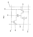
- FIG. 1 shows a unit pixel of the conventional CMOS image sensor.
- the reference numeral 001 indicates a photoelectric-conversion photodiode.
- the reference numerals 006, 007 and 008 indicate an amplification transistor, a reset transistor and a selection transistor, respectively.
- the reference numerals 004, 002, 003, 005 and 009 indicate a signal line, a pixel-selection clock line, a reset clock line, a power supply line, and a reset power supply line, respectively.
- the unit pixel of the conventional CMOS image sensor has the photodiode and the three MOS transistors in a plane. Thus, it is difficult to increase a ratio of a surface area of a light-receiving section (photodiode) to an overall surface area of one pixel.
- Non-Patent Document 1 It is reported that, in a conventional CMOS image sensor using a 0.35 ⁇ m, single polysilicon layer/double metal layer CMOS process, a ratio of a surface area of a light-receiving section (photodiode) to an overall surface area of one pixel is 17% (see the following Non-Patent Document 1). It is also reported that, in a conventional CMOS image sensor using a 0.15 ⁇ m wiring-rule process, a ratio of a surface area of a light-receiving section (photodiode) to an overall surface area of one pixel is 30% (see the following Non-Patent Document 2).
- CMOS image sensor where the ratio of the surface area of the light-receiving section (photodiode) to the overall surface area of one pixel is 30%, a microlens is formed to condense light. This means that a CMOS image sensor having a small ratio of a surface area of a light-receiving section (photodiode) to an overall surface area of one pixel requires a light-condensing microlens.
- a solid-state imaging device which comprises a signal line formed on a substrate, an island-shaped semiconductor arranged on the signal line, and a pixel selection line connected to a top of the island-shaped semiconductor.
- the island-shaped semiconductor includes: a first semiconductor layer formed as a bottom portion of the island-shaped semiconductor and connected to the signal line; a second semiconductor layer formed above and adjacent to the first semiconductor layer; a gate connected to the second semiconductor layer through a dielectric film; a charge storage section comprised of a third semiconductor layer connected to the second semiconductor layer and adapted, in response to receiving light, to undergo a change in amount of electric charges therein; and a fourth semiconductor layer formed above and adjacent to the second and third semiconductor layers.
- the pixel selection line is comprised of a transparent conductive film, and a part of the gate is disposed inside a depression formed in a sidewall of the second semiconductor layer.
- the signal line is an n+-type diffusion layer.
- the first semiconductor layer is an n+-type diffusion layer, and the second semiconductor layer is a p-type impurity-doped region.
- the third semiconductor layer is an n-type diffusion layer, and the fourth semiconductor layer is a p+-type diffusion layer.
- a combination of the p+-type diffusion layer and the n-type diffusion layer functions as a photoelectric-conversion photodiode
- a combination of the p+-type diffusion layer, the n-type diffusion layer and the p-type impurity-doped region functions as an amplification transistor.
- a combination of the n+-type diffusion layer serving as the first semiconductor layer, the p-type impurity-doped region, the n-type diffusion layer and the gate functions as a reset transistor
- a combination of the p-type impurity-doped region and the n+-type diffusion layer serving as the first semiconductor layer functions as a diode.
- the island-shaped semiconductor may have a square or rectangular pillar shape.
- the island-shaped semiconductor may have a hexagonal pillar shape.
- the island-shaped semiconductor may have a circular pillar shape.
- a solid-state imaging apparatus which comprises a plurality of the solid-state imaging devices according to the first aspect of the present invention, wherein the solid-state imaging devices are arranged in an n-row by m-column array (wherein each of n and m is an integer of 1 or more) with respect to the substrate.
- a solid-state imaging apparatus which comprises a plurality of the solid-state imaging devices each including the island-shaped semiconductor having a square or rectangular pillar shape, wherein the solid-state imaging devices are arranged in an n-row by m-column array (wherein each of n and m is an integer of 1 or more) with respect to the substrate.
- a solid-state imaging apparatus which comprises a plurality of the solid-state imaging devices each including the island-shaped semiconductor having a circular pillar shape, wherein the solid-state imaging devices are arranged in an n-row by m-column array (wherein each of n and m is an integer of 1 or more) with respect to the substrate.
- a solid-state imaging apparatus which comprises a plurality of the solid-state imaging devices according to the first aspect of the present invention, wherein the solid-state imaging devices are arranged on the substrate in a honeycomb pattern.
- a solid-state imaging apparatus which comprises a plurality of the solid-state imaging devices each including the island-shaped semiconductor having a hexagonal pillar shape, wherein the solid-state imaging devices are arranged on the substrate in a honeycomb pattern.
- a solid-state imaging apparatus which comprises a plurality of the solid-state imaging devices each including the island-shaped semiconductor having a circular pillar shape, wherein the solid-state imaging devices are arranged on the substrate in a honeycomb pattern.
- a method of producing a solid-state imaging device comprises the steps of: forming an oxide film on a silicon substrate; forming a p-type silicon on the oxide film; forming an oxide film-based mask and a nitride film-based mask by depositing a nitride film on the p-type silicon, depositing an oxide film on the nitride film, forming a resist for a silicon pillar, etching the oxide film and the nitride film, and removing the resist; forming a depression in a sidewall of a p-type impurity-doped region by etching the p-type silicon to form a silicon pillar, depositing a nitride film, etching the nitride film in such a manner that a sidewall-shaped nitride film is left on a sidewall of the silicon pillar, and isotropically etching the p-type silicon;
- a unit pixel of a conventional CMOS image sensor has a total four elements, i.e., a photodiode and three MOS transistors, in a plane. Thus, it is difficult to increase a ratio of a surface area of a light-receiving section (photodiode) to an overall surface area of one pixel. It is reported that, in a conventional CMOS image sensor using a 0.15 ⁇ m wiring-rule process, a ratio of a surface area of a light-receiving section (photodiode) to an overall surface area of one pixel is 30%.
- the present invention provides a solid-state imaging device which comprises: a signal line formed on a substrate; an island-shaped semiconductor arranged on the signal line; and a pixel selection line connected to a top of the island-shaped semiconductor, wherein the island-shaped semiconductor includes: a first semiconductor layer formed as a bottom portion of the island-shaped semiconductor and connected to the signal line; a second semiconductor layer formed above and adjacent to the first semiconductor layer; a gate connected to the second semiconductor layer through a dielectric film; a charge storage section comprised of a third semiconductor layer connected to the second semiconductor layer and adapted, in response to receiving light, to undergo a change in amount of electric charges therein; and a fourth semiconductor layer formed above and adjacent to the second and third semiconductor layers, and wherein the pixel selection line is comprised of a transparent conductive film, and a part of the gate is disposed inside a depression formed in a sidewall of the second semiconductor layer.
- a combination of the third and fourth semiconductor layers, a combination of the second, third and fourth semiconductor layers, a combination of the first, second and third semiconductor layers, and a combination of the second and first semiconductor layers function, respectively, as the photoelectric-conversion photodiode, the amplification transistor, the reset transistor, and the diode in the aforementioned unit pixel.
- a metal for use in a conventional semiconductor production process such as aluminum or copper, reflects light. Thus, it is necessary to connect a line made of such a metal to a sidewall of the fourth semiconductor layer.
- a transparent conductive film such as indium tin oxide (ITO), zinc oxide (ZnO) or tin oxide (SnO 2 ), is used as the pixel selection line to allow the pixel selection line to be connected to a top of the fourth semiconductor layer.
- ITO indium tin oxide
- ZnO zinc oxide
- SnO 2 tin oxide
- a surface area of one pixel is a sum of an area of the photodiode, an area of the gate, and an area of a region between the devices.
- a part of the gate is disposed inside a depression formed in a sidewall of the second semiconductor layer, so that a surface area of one pixel can be reduced substantially to a sum of an area of the photodiode and an area of a region between the devices.
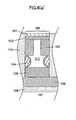
- FIG. 2 is a bird's-eye view showing a single solid-state imaging device according to a first embodiment of the present invention.
- FIG. 3 is a top plan view showing the solid-state imaging device according to the first embodiment.
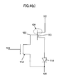
- FIG. 4(a) is a sectional view taken along the line X 1 -X' 1 in FIG. 3
- FIG. 4(b) is a diagram showing an equivalent circuit of the sectional structure in FIG. 4(a)
- FIG. 5(a) is a sectional view taken along the line Y 1 -Y' 1 in FIG. 3
- FIG. 5(b) is a diagram showing an equivalent circuit of the sectional structure in FIG. 5(a) .
- an oxide film 108 is formed on a silicon substrate 107.
- a signal line 106 is formed on the oxide film 108, and an island-shaped semiconductor is formed on the signal line 106.
- the island-shaped semiconductor comprises: an n+-type diffusion layer 105 formed as a bottom portion thereof and connected to the signal line; a p-type impurity-doped region 111 formed above and adjacent to the n+-type diffusion layer; a gate 104 connected to the p-type impurity-doped region through a dielectric film; a charge storage section 103 comprised of an n-type diffusion layer connected to the p-type impurity-doped region 111 and adapted, in response to receiving light, to undergo a change in amount of electric charges therein; and a p+-type diffusion layer 102 formed above and adjacent to the p-type impurity-doped region and the n-type diffusion layer.
- a pixel selection line 101 comprised of a transparent conductive film is formed to be connected to a top of the p+-type diffusion layer 102 which is a top portion of the island-shaped semiconductor.
- the gate is formed in such a manner that a part thereof is disposed inside a depression formed in a sidewall of the p-type impurity-doped region.
- a combination of the p+-type diffusion layer 102 and the n-type diffusion layer 103 functions as a photoelectric-conversion photodiode 109.
- a combination of the p+-type diffusion layer 102, the n-type diffusion layer 103 and the p-type impurity-doped region 111 functions as an amplification transistor 113.
- a combination of the n+-type diffusion layer 105, the p-type impurity-doped region 111, the n-type diffusion layer 103 and the gate 104 functions as a reset transistor 112.
- a combination of the p-type impurity-doped region 111 and the n+-type diffusion layer 105 functions as a diode 114.
- An oxide film 110 is formed as an interlayer dielectric film.
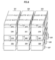
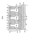
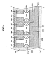
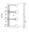
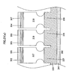
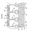
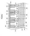
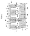
- FIG. 6 is a bird's-eye view showing a solid-state imaging device array in which a plurality of the above solid-state imaging devices are arranged in a matrix pattern.
- FIG. 7 is a top plan view of the solid-state imaging device array.
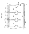
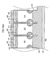
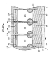
- FIG. 8 , FIG. 9 , FIG. 10 and FIG. 11 are a sectional view taken along the line X 2 -X' 2 in FIG. 7 , a sectional view taken along the line X 3 -X' 3 in FIG. 7 , a sectional view taken along the line X 4 -X' 4 in FIG. 7 and a sectional view taken along the line Y 2 -Y' 2 in FIG. 7 , respectively.
- an oxide film 241 is formed on a silicon substrate 242.
- a signal line 225 is formed on the oxide film 241, and a first island-shaped semiconductor is formed on the signal line 225.
- the first island-shaped semiconductor comprises: an n+-type diffusion layer 237 formed as a bottom portion thereof and connected to the signal line 225; a p-type impurity-doped region 234 formed above and adjacent to the n+-type diffusion layer 237; a gate 219 connected to the p-type impurity-doped region 234 through a dielectric film; a charge storage section 231 comprised of an n-type diffusion layer connected to the p-type impurity-doped region 234 and adapted, in response to receiving light, to undergo a change in amount of electric charges therein; and a p+-type diffusion layer 228 formed above and adjacent to the p-type impurity-doped region 234 and the n-type diffusion layer 231.
- a pixel selection line 201 comprised of a transparent conductive film is formed to be connected to a top of the p+-type diffusion layer 228 which is a top portion of the first island-shaped semiconductor.
- the gate 219 is formed in such a manner that a part thereof is disposed inside a depression formed in a sidewall of the p-type impurity-doped region 234.
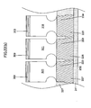
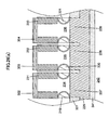
- a second island-shaped semiconductor is formed on the signal line 225 formed on the oxide film 241 formed on the silicon substrate 242.
- the second island-shaped semiconductor comprises: an n+-type diffusion layer 238 formed as a bottom portion thereof and connected to the signal line 225; a p-type impurity-doped region 235 formed above and adjacent to the n+-type diffusion layer 238; a gate 220 connected to the p-type impurity-doped region 235 through a dielectric film; a charge storage section 232 comprised of an n-type diffusion layer connected to the p-type impurity-doped region 235 and adapted, in response to receiving light, to undergo a change in amount of electric charges therein; and a p+-type diffusion layer 229 formed above and adjacent to the p-type impurity-doped region 235 and the n-type diffusion layer 232.
- a pixel selection line 202 comprised of a transparent conductive film is formed to be connected to a top of the p+-type diffusion layer 229 which is a top portion of the second island-shaped semiconductor.
- the gate 220 is formed in such a manner that a part thereof is disposed inside a depression formed in a sidewall of the p-type impurity-doped region 235.
- a third island-shaped semiconductor is formed on the signal line 225 formed on the oxide film 241 formed on the silicon substrate 242.
- the third island-shaped semiconductor comprises: an n+-type diffusion layer 239 formed as a bottom portion thereof and connected to the signal line 225; a p-type impurity-doped region 236 formed above and adjacent to the n+-type diffusion layer 239; a gate 221 connected to the p-type impurity-doped region 236 through a dielectric film; a charge storage section 233 comprised of an n-type diffusion layer connected to the p-type impurity-doped region 236 and adapted, in response to receiving light, to undergo a change in amount of electric charges therein; and a p+-type diffusion layer 230 formed above and adjacent to the p-type impurity-doped region 236 and the n-type diffusion layer 233.
- a pixel selection line 203 comprised of a transparent conductive film is formed to be connected to a top of the p+-type diffusion layer 230 which is a top portion of the third island-shaped semiconductor.
- the gate 221 is formed in such a manner that a part thereof is disposed inside a depression formed in a sidewall of the p-type impurity-doped region 236.
- An oxide film 240 is formed as an interlayer dielectric film.
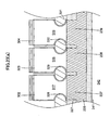
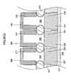
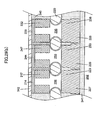
- a signal line 226 is formed on the oxide film 241 formed on the silicon substrate 242, and a fourth island-shaped semiconductor is formed on the signal line 226.
- the fourth island-shaped semiconductor comprises: an n+-type diffusion layer 252 formed as a bottom portion thereof and connected to the signal line 226; a p-type impurity-doped region 249 formed above and adjacent to the n+-type diffusion layer 252; a gate 219 connected to the p-type impurity-doped region 249 through a dielectric film; a charge storage section 246 comprised of an n-type diffusion layer connected to the p-type impurity-doped region 249 and adapted, in response to receiving light, to undergo a change in amount of electric charges therein; and a p+-type diffusion layer 243 formed above and adjacent to the p-type impurity-doped region 249 and the n-type diffusion layer 246.
- the pixel selection line 201 comprised of a transparent conductive film is formed to be connected to a top of the p+-type diffusion layer 243 which is a top portion of the fourth island-shaped semiconductor.
- the gate 219 is formed in such a manner that a part thereof is disposed inside a depression formed in a sidewall of the p-type impurity-doped region 249.
- a fifth island-shaped semiconductor is formed on the signal line 226 formed on the oxide film 241 formed on the silicon substrate 242.
- the fifth island-shaped semiconductor comprises: an n+-type diffusion layer 253 formed as a bottom portion thereof and connected to the signal line 226; a p-type impurity-doped region 250 formed above and adjacent to the n+-type diffusion layer 253; a gate 220 connected to the p-type impurity-doped region 250 through a dielectric film; a charge storage section 247 comprised of an n-type diffusion layer connected to the p-type impurity-doped region 250 and adapted, in response to receiving light, to undergo a change in amount of electric charges therein; and a p+-type diffusion layer 244 formed above and adjacent to the p-type impurity-doped region 250 and the n-type diffusion layer 247.
- the pixel selection line 202 comprised of a transparent conductive film is formed to be connected to a top of the p+-type diffusion layer 244 which is a top portion of the fifth island-shaped semiconductor.
- the gate 220 is formed in such a manner that a part thereof is disposed inside a depression formed in a sidewall of the p-type impurity-doped region 250.
- a sixth island-shaped semiconductor is formed on the signal line 226 formed on the oxide film 241 formed on the silicon substrate 242.
- the sixth island-shaped semiconductor comprises: an n+-type diffusion layer 254 formed as a bottom portion thereof and connected to the signal line 226; a p-type impurity-doped region 251 formed above and adjacent to the n+-type diffusion layer 254; a gate 221 connected to the p-type impurity-doped region 251 through a dielectric film; a charge storage section 248 comprised of an n-type diffusion layer connected to the p-type impurity-doped region 251 and adapted, in response to receiving light, to undergo a change in amount of electric charges therein; and a p+-type diffusion layer 245 formed above and adjacent to the p-type impurity-doped region 251 and the n-type diffusion layer 248.
- the pixel selection line 203 comprised of a transparent conductive film is formed to be connected to a top of the p+-type diffusion layer 245 which is a top portion of the sixth island-shaped semiconductor.
- the gate 221 is formed in such a manner that a part thereof is disposed inside a depression formed in a sidewall of the p-type impurity-doped region 251.
- the oxide film 240 is formed as an interlayer dielectric film.
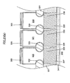
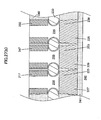
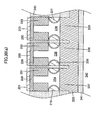
- a signal line 227 is formed on the oxide film 241 formed on the silicon substrate 242, and a seventh island-shaped semiconductor is formed on the signal line 227.
- the seventh island-shaped semiconductor comprises: an n+-type diffusion layer 222 formed as a bottom portion thereof and connected to the signal line 227; a p-type impurity-doped region 255 formed above and adjacent to the n+-type diffusion layer 222; a gate 219 connected to the p-type impurity-doped region 255 through a dielectric film; a charge storage section 216 comprised of an n-type diffusion layer connected to the p-type impurity-doped region 255 and adapted, in response to receiving light, to undergo a change in amount of electric charges therein; and a p+-type diffusion layer 213 formed above and adjacent to the p-type impurity-doped region 255 and the n-type diffusion layer 216.
- the pixel selection line 201 comprised of a transparent conductive film is formed to be connected to a top of the p+-type diffusion layer 213 which is a top portion of the seventh island-shaped semiconductor.
- the gate 219 is formed in such a manner that a part thereof is disposed inside a depression formed in a sidewall of the p-type impurity-doped region 255.
- An eighth island-shaped semiconductor is formed on the signal line 227 formed on the oxide film 241 formed on the silicon substrate 242.
- the eighth island-shaped semiconductor comprises: an n+-type diffusion layer 223 formed as a bottom portion thereof and connected to the signal line 227; a p-type impurity-doped region 256 formed above and adjacent to the n+-type diffusion layer 223; a gate 220 connected to the p-type impurity-doped region 256 through a dielectric film; a charge storage section 217 comprised of an n-type diffusion layer connected to the p-type impurity-doped region 256 and adapted, in response to receiving light, to undergo a change in amount of electric charges therein; and a p+-type diffusion layer 214 formed above and adjacent to the p-type impurity-doped region 256 and the n-type diffusion layer 217.
- the pixel selection line 202 comprised of a transparent conductive film is formed to be connected to a top of the p+-type diffusion layer 214 which is a top portion of the eighth island-shaped semiconductor.
- the gate 220 is formed in such a manner that a part thereof is disposed inside a depression formed in a sidewall of the p-type impurity-doped region 256.
- a ninth island-shaped semiconductor is formed on the signal line 227 formed on the oxide film 241 formed on the silicon substrate 242.
- the ninth island-shaped semiconductor comprises: an n+-type diffusion layer 224 formed as a bottom portion thereof and connected to the signal line 227; a p-type impurity-doped region 257 formed above and adjacent to the n+-type diffusion layer 224; a gate 221 connected to the p-type impurity-doped region 257 through a dielectric film; a charge storage section 218 comprised of an n-type diffusion layer connected to the p-type impurity-doped region 257 and adapted, in response to receiving light, to undergo a change in amount of electric charges therein; and a p+-type diffusion layer 215 formed above and adjacent to the p-type impurity-doped region 257 and the n-type diffusion layer 218.
- the pixel selection line 203 comprised of a transparent conductive film is formed to be connected to a top of the p+-type diffusion layer 215 which is a top portion of the eighth island-shaped semiconductor.
- the gate 221 is formed in such a manner that a part thereof is disposed inside a depression formed in a sidewall of the p-type impurity-doped region 257.
- the oxide film 240 is formed as an interlayer dielectric film.
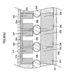
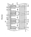
- the eighth island-shaped semiconductor is formed on the signal line 227 formed on the oxide film 241 formed on the silicon substrate 242.
- the eighth island-shaped semiconductor comprises: the n+-type diffusion layer 223 formed as a bottom portion thereof and connected to the signal line 227; the p-type impurity-doped region 256 formed above and adjacent to the n+-type diffusion layer 223; the gate 220 connected to the p-type impurity-doped region 256 through the dielectric film; the charge storage section 217 comprised of an n-type diffusion layer connected to the p-type impurity-doped region 256 and adapted, in response to receiving light, to undergo a change in amount of electric charges therein; and the p+-type diffusion layer 214 formed above and adjacent to the p-type impurity-doped region 256 and the n-type diffusion layer 217.
- the pixel selection line 202 comprised of a transparent conductive film is formed to be connected to the top of the p+-type diffusion layer 214 which is the top portion of the eighth island-shaped semiconductor.
- the gate 220 is formed in such a manner that the part thereof is disposed inside the depression formed in the sidewall of the p-type impurity-doped region 256.
- the fifth island-shaped semiconductor is formed on the signal line 226 formed on the oxide film 241 formed on the silicon substrate 242.
- the fifth island-shaped semiconductor comprises: the n+-type diffusion layer 253 formed as a bottom portion thereof and connected to the signal line 226; the p-type impurity-doped region 250 formed above and adjacent to the n+-type diffusion layer 253; the gate 220 connected to the p-type impurity-doped region 250 through the dielectric film; the charge storage section 247 comprised of an n-type diffusion layer connected to the p-type impurity-doped region 250 and adapted, in response to receiving light, to undergo a change in amount of electric charges therein; and the p+-type diffusion layer 244 formed above and adjacent to the p-type impurity-doped region 250 and the n-type diffusion layer 247.
- the pixel selection line 202 comprised of a transparent conductive film is formed to be connected to the top of the p+-type diffusion layer 244 which is the top portion of the fifth island-shaped semiconductor.
- the gate 220 is formed in such a manner that the part thereof is disposed inside the depression formed in the sidewall of the p-type impurity-doped region 250.
- the second island-shaped semiconductor is formed on the signal line 225 formed on the oxide film 241 formed on the silicon substrate 242.
- the second island-shaped semiconductor comprises: the n+-type diffusion layer 238 formed as a bottom portion thereof and connected to the signal line 225; the p-type impurity-doped region 235 formed above and adjacent to the n+-type diffusion layer 238; the gate 220 connected to the p-type impurity-doped region 235 through the dielectric film; the charge storage section 232 comprised of an n-type diffusion layer connected to the p-type impurity-doped region 235 and adapted, in response to receiving light, to undergo a change in amount of electric charges therein; and the p+-type diffusion layer 229 formed above and adjacent to the p-type impurity-doped region 235 and the n-type diffusion layer 232.
- the pixel selection line 202 comprised of a transparent conductive film is formed to be connected to the top of the p+-type diffusion layer 229 which is the top portion of the second island-shaped semiconductor.
- the gate 220 is formed in such a manner that the part thereof is disposed inside the depression formed in the sidewall of the p-type impurity-doped region 235.
- FIGS. 12(a) to 31(b) one example of a production process for forming a solid-state imaging device structure according to the present invention will be described below.
- an oxide film 241 is formed on a silicon substrate 242.
- a p-type silicon 301 is formed on the oxide film 241.
- a nitride film is deposited on the p-type silicon 301, and an oxide film is deposited on the nitride film.
- the oxide film and the nitride film are etched to form an oxide film-based mask (305, 306, 307, 310, 311) and a nitride film-based mask (302, 303, 304, 308, 309) on the p-type silicon 301, and then the resist is removed ( FIGS. 12(a) and 12(b) ).
- the p-type silicon is etched ( FIGS. 13(a) and 13(b) ) to form a silicon pillar.
- a nitride film is deposited and then etched in such a manner that a sidewall-shaped nitride film (312, 313, 314, 315, 316) is left on a sidewall of the silicon pillar ( FIGS. 14(a) and 14(b) ).
- the p-type silicon is isotropically etched to form a depression in a sidewall of a p-type impurity-doped region ( FIGS. 15(a) and 15(b) ).
- the p-type silicon is etched to form an island-shaped semiconductor (317, 318, 319, 320, 321) having the depression in the sidewall of the p-type impurity-doped region ( FIGS. 16(a) and 16(b) ).
- a thin oxide film 322 is formed to prevent ion channeling during ion implantation ( FIGS. 17(a) and 17(b) ).
- a continuous n+-type diffusion layer 323 is formed through phosphorus (P) implantation and annealing ( FIGS. 18(a) and 18(b) ).
- a resist (324, 325, 326) for a signal line is formed ( FIGS. 19(a) and 19(b) ).
- the thin oxide film and the silicon are etched to form an n+-type diffusion layer (237, 238, 239, 223, 256) and a signal line (225, 226, 227) ( FIGS. 20(a) and 20(b) ).
- FIGS. 21 (a) and 21 (b) The resist, the sidewall-shaped nitride film and the thin oxide film are removed ( FIGS. 21 (a) and 21 (b) ).
- An oxide film 327 is deposited and then subjected to flattening and etching-back ( FIGS. 22(a) and 22(b) ).
- a gate dielectric film (328, 329, 330, 332, 333) is formed. Subsequently, polysilicon is deposited and then subjected to flattening and etching-back ( FIGS. 23(a) and 23(b) ).
- a resist (334, 335, 336) for a gate is formed ( FIGS. 24(a) and 24(b) ).
- the polysilicon is etched to form a gate (219, 220, 221), and then the resist is removed ( FIGS. 25(a) and 25(b) ).
- Phosphorus (P) is implanted to form a charge storage section (231, 232, 233, 217, 247) ( FIGS. 26(a) and 26(b) ).
- An oxide film 240 is deposited and then subjected to flattening and etching-back. Then, the nitride film on the island-shaped semiconductor is removed ( FIGS. 27(a) and 27(b) ).
- An oxide film (337, 338, 339, 340, 341) is formed. Subsequently, a p+-type diffusion layer (228, 229, 230, 214, 244) is formed through boron (B) implantation and annealing ( FIGS. 28(a) and 28(b) ).
- FIGS. 29(a) and 29(b) The oxide film is removed, and then a transparent conductive film 342 is deposited ( FIGS. 29(a) and 29(b) ).
- a resist for a pixel selection line is formed, and then the transparent conductive film is etched to form a pixel selection line (201, 202, 203). Then, the resist is removed ( FIGS. 30(a) and 30(b) ).
- a surface protection film 343 is formed ( FIGS. 31 (a) and 31 (b) ).
- a cross-sectional shape of the depression in the sidewall of the p-type impurity-doped region is a semicircular shape.
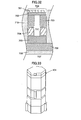
- the depression may be formed in any other suitable shape, such as a cross-sectionally rectangular shape as shown in FIG. 32 .
- FIG. 32 is a sectional view showing a solid-state imaging device according a second embodiment of the present invention.
- an oxide film 708 is formed on a silicon substrate 707.
- a signal line 706 is formed on the oxide film 708, and an island-shaped semiconductor is formed on the signal line 706.
- the island-shaped semiconductor comprises: an n+-type diffusion layer 705 formed as a bottom portion thereof and connected to the signal line; a p-type impurity-doped region 711 formed above and adjacent to the n+-type diffusion layer; a gate 704 connected to the p-type impurity-doped region through a dielectric film; a charge storage section 703 comprised of an n-type diffusion layer connected to the p-type impurity-doped region and adapted, in response to receiving light, to undergo a change in amount of electric charges therein; and a p+-type diffusion layer 702 formed above and adjacent to the p-type impurity-doped region and the n-type diffusion layer.
- a pixel selection line 701 comprised of a transparent conductive film is formed to be connected to a top of the p+-type diffusion layer which is a top portion of the island-shaped semiconductor.
- the gate is formed in such a manner that a part thereof is disposed inside a depression which is formed in a sidewall of the p-type impurity-doped region to have a square or rectangular shape in cross-section.
- a combination of the p+-type diffusion layer 702 and the n-type diffusion layer 703 functions as a photoelectric-conversion photodiode 709.
- An oxide film 710 is formed as an interlayer dielectric film.
- Each of the first and second embodiments shows a solid-state imaging device comprising an island-shaped semiconductor having a square or rectangular pillar shape.
- the solid-state imaging device may comprise an island-shaped semiconductor having a hexagonal pillar shape, as shown in FIG. 33 .
- the first embodiment shows a solid-state imaging device array in which a plurality of solid-state imaging devices each comprising an island-shaped semiconductor having a square or rectangular pillar shape are arranged in an n-row by m-column array (wherein each of n and m is an integer of 1 or more.) with respect to a substrate. For example, as shown in FIG.
- the 1st solid-state imaging device column consisting of three solid-state imaging devices 402, 403, 404 each comprising an island-shaped semiconductor having a hexagonal pillar shape
- the 2nd solid-state imaging device column consisting of three solid-state imaging devices 405, 406, 407 each comprising an island-shaped semiconductor having a hexagonal pillar shape
- the 3rd solid-state imaging device column consisting of three solid-state imaging devices 408, 409, 410 each comprising an island-shaped semiconductor having a hexagonal pillar shape
- the solid-state imaging device array may be arranged in a honeycomb pattern.
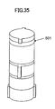
- each of the first and second embodiments shows a solid-state imaging device comprising an island-shaped semiconductor having a square or rectangular pillar shape.
- the solid-state imaging device may comprise an island-shaped semiconductor 501 having a circular pillar shape, as shown in FIG. 35 .
- the present invention provides a solid-state imaging device which comprises: a signal line formed on a substrate; an island-shaped semiconductor arranged on the signal line; and a pixel selection line connected to a top of the island-shaped semiconductor, wherein the island-shaped semiconductor includes: a first semiconductor layer formed as a bottom portion of the island-shaped semiconductor and connected to the signal line; a second semiconductor layer formed above and adjacent to the first semiconductor layer; a gate connected to the second semiconductor layer through a dielectric film; a charge storage section comprised of a third semiconductor layer connected to the second semiconductor layer and adapted, in response to receiving light, to undergo a change in amount of electric charges therein; and a fourth semiconductor layer formed above and adjacent to the second and third semiconductor layers, and wherein the pixel selection line is comprised of a transparent conductive film, and a part of the gate is disposed inside a depression formed in a sidewall of the second semiconductor layer.
- a combination of the third and fourth semiconductor layers, a combination of the second, third and fourth semiconductor layers, a combination of the first, second and third semiconductor layers, and a combination of the second and first semiconductor layers function, respectively, as the photoelectric-conversion photodiode, the amplification transistor, the reset transistor, and the diode in the aforementioned unit pixel.
- a metal for use in a conventional semiconductor production process such as aluminum or copper, reflects light. Thus, it is necessary to connect a line made of such a metal to a sidewall of the fourth semiconductor layer.
- a transparent conductive film such as indium tin oxide (ITO), zinc oxide (ZnO) or tin oxide (SnO 2 ) is used as the pixel selection line to allow the pixel selection line to be connected to a top of the fourth semiconductor layer.
- ITO indium tin oxide
- ZnO zinc oxide
- SnO 2 tin oxide
- a surface area of one pixel is a sum of an area of the photodiode, an area of the gate, and an area of a region between the devices.
- a part of the gate is disposed inside a depression formed in a sidewall of the second semiconductor layer, so that a surface area of one pixel can be reduced substantially to a sum of an area of the photodiode and an area of a region between the devices.
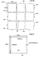
- FIG. 36 is a top plan view showing a solid-state imaging apparatus in which nine image sensors 601, 602, 603, 604, 605, 606, 607, 608, 609 each comprising the island-shaped semiconductor having a square pillar shape according to the present invention are arranged in a matrix array.
- FIG. 36 is a top plan view showing a solid-state imaging apparatus in which nine image sensors 601, 602, 603, 604, 605, 606, 607, 608, 609 each comprising the island-shaped semiconductor having a square pillar shape according to the present invention are arranged in a matrix array.
- FIG. 37 is an enlarged top plan view showing a light-receiving section 610 in one pixel of the solid-state imaging apparatus.
- F indicates a wiring rule.
- a 0.15 ⁇ m wiring-rule process is used on an assumption that a surface area per pixel is 2 ⁇ m ⁇ 2 ⁇ m.
- a surface area of the light-receiving section (photodiode) is 1.925 ⁇ m ⁇ 1.925 ⁇ m.
- a ratio of a surface area of a light-receiving section (photodiode) to an overall surface area of one pixel is 92.6%.
- a surface area of a unit pixel of an image sensor is largely occupied by a surface area of the photodiode, and it is possible to provide an image sensor having a sufficiently-large ratio of a surface area of a light-receiving section to an overall surface area of one pixel.
Landscapes
- Physics & Mathematics (AREA)
- Engineering & Computer Science (AREA)
- Power Engineering (AREA)
- Electromagnetism (AREA)
- Condensed Matter Physics & Semiconductors (AREA)
- General Physics & Mathematics (AREA)
- Computer Hardware Design (AREA)
- Microelectronics & Electronic Packaging (AREA)
- Solid State Image Pick-Up Elements (AREA)
- Transforming Light Signals Into Electric Signals (AREA)
Applications Claiming Priority (2)
| Application Number | Priority Date | Filing Date | Title |
|---|---|---|---|
| PCT/JP2008/058412 WO2009133623A1 (ja) | 2008-05-02 | 2008-05-02 | 固体撮像素子 |
| PCT/JP2009/058629 WO2009133957A1 (ja) | 2008-05-02 | 2009-05-07 | 固体撮像素子 |
Publications (2)
| Publication Number | Publication Date |
|---|---|
| EP2290692A1 true EP2290692A1 (de) | 2011-03-02 |
| EP2290692A4 EP2290692A4 (de) | 2012-05-02 |
Family
ID=41254853
Family Applications (1)
| Application Number | Title | Priority Date | Filing Date |
|---|---|---|---|
| EP09738894A Withdrawn EP2290692A4 (de) | 2008-05-02 | 2009-05-07 | Halbleiter-bilderfassungselement |
Country Status (5)
| Country | Link |
|---|---|
| EP (1) | EP2290692A4 (de) |
| KR (1) | KR101113905B1 (de) |
| CN (1) | CN102017151B (de) |
| TW (1) | TW200947691A (de) |
| WO (2) | WO2009133623A1 (de) |
Families Citing this family (16)
| Publication number | Priority date | Publication date | Assignee | Title |
|---|---|---|---|---|
| US8183628B2 (en) | 2007-10-29 | 2012-05-22 | Unisantis Electronics Singapore Pte Ltd. | Semiconductor structure and method of fabricating the semiconductor structure |
| JP5317343B2 (ja) | 2009-04-28 | 2013-10-16 | ユニサンティス エレクトロニクス シンガポール プライベート リミテッド | 半導体装置及びその製造方法 |
| US8598650B2 (en) | 2008-01-29 | 2013-12-03 | Unisantis Electronics Singapore Pte Ltd. | Semiconductor device and production method therefor |
| JP5356970B2 (ja) | 2009-10-01 | 2013-12-04 | ユニサンティス エレクトロニクス シンガポール プライベート リミテッド | 半導体装置 |
| WO2011111662A1 (ja) * | 2010-03-08 | 2011-09-15 | 日本ユニサンティスエレクトロニクス株式会社 | 固体撮像装置 |
| JP5054182B2 (ja) * | 2010-03-12 | 2012-10-24 | ユニサンティス エレクトロニクス シンガポール プライベート リミテッド | 固体撮像装置 |
| US8487357B2 (en) | 2010-03-12 | 2013-07-16 | Unisantis Electronics Singapore Pte Ltd. | Solid state imaging device having high sensitivity and high pixel density |
| JP5066590B2 (ja) | 2010-06-09 | 2012-11-07 | ユニサンティス エレクトロニクス シンガポール プライベート リミテッド | 半導体装置とその製造方法 |
| JP5087655B2 (ja) | 2010-06-15 | 2012-12-05 | ユニサンティス エレクトロニクス シンガポール プライベート リミテッド | 半導体装置及びその製造方法 |
| JP4769911B1 (ja) * | 2010-10-29 | 2011-09-07 | 日本ユニサンティスエレクトロニクス株式会社 | 固体撮像装置 |
| JP4769910B1 (ja) * | 2011-02-18 | 2011-09-07 | 日本ユニサンティスエレクトロニクス株式会社 | 固体撮像装置 |
| US8564034B2 (en) | 2011-09-08 | 2013-10-22 | Unisantis Electronics Singapore Pte. Ltd. | Solid-state imaging device |
| US8669601B2 (en) | 2011-09-15 | 2014-03-11 | Unisantis Electronics Singapore Pte. Ltd. | Method for producing semiconductor device and semiconductor device having pillar-shaped semiconductor |
| US8772175B2 (en) | 2011-12-19 | 2014-07-08 | Unisantis Electronics Singapore Pte. Ltd. | Method for manufacturing semiconductor device and semiconductor device |
| US8916478B2 (en) | 2011-12-19 | 2014-12-23 | Unisantis Electronics Singapore Pte. Ltd. | Method for manufacturing semiconductor device and semiconductor device |
| US8748938B2 (en) | 2012-02-20 | 2014-06-10 | Unisantis Electronics Singapore Pte. Ltd. | Solid-state imaging device |
Citations (2)
| Publication number | Priority date | Publication date | Assignee | Title |
|---|---|---|---|---|
| WO2001022494A1 (de) * | 1999-09-21 | 2001-03-29 | Infineon Technologies Ag | Vertikale pixelzellen |
| US20070181925A1 (en) * | 2006-02-09 | 2007-08-09 | Jae-Man Yoon | Semiconductor device having a vertical channel and method of manufacturing same |
Family Cites Families (8)
| Publication number | Priority date | Publication date | Assignee | Title |
|---|---|---|---|---|
| JPS6417462A (en) * | 1987-07-11 | 1989-01-20 | Sony Corp | Read-only memory device |
| JPH01175775A (ja) * | 1987-12-29 | 1989-07-12 | Sharp Corp | 光駆動mos型半導体装置 |
| JPH0289368A (ja) * | 1988-09-27 | 1990-03-29 | Sony Corp | 固体撮像装置 |
| JP3621844B2 (ja) | 1999-02-24 | 2005-02-16 | シャープ株式会社 | 増幅型固体撮像装置 |
| JP3713418B2 (ja) * | 2000-05-30 | 2005-11-09 | 光正 小柳 | 3次元画像処理装置の製造方法 |
| JP4714998B2 (ja) | 2001-02-14 | 2011-07-06 | ソニー株式会社 | 固体撮像素子 |
| JP3899236B2 (ja) * | 2001-02-16 | 2007-03-28 | シャープ株式会社 | イメージセンサの製造方法 |
| JP4218894B2 (ja) | 2004-07-08 | 2009-02-04 | シャープ株式会社 | 固体撮像装置およびその製造方法 |
-
2008
- 2008-05-02 WO PCT/JP2008/058412 patent/WO2009133623A1/ja active Application Filing
-
2009
- 2009-04-29 TW TW098114145A patent/TW200947691A/zh unknown
- 2009-05-07 CN CN2009801158772A patent/CN102017151B/zh not_active Expired - Fee Related
- 2009-05-07 WO PCT/JP2009/058629 patent/WO2009133957A1/ja active Application Filing
- 2009-05-07 EP EP09738894A patent/EP2290692A4/de not_active Withdrawn
- 2009-05-07 KR KR1020107024780A patent/KR101113905B1/ko active IP Right Grant
Patent Citations (2)
| Publication number | Priority date | Publication date | Assignee | Title |
|---|---|---|---|---|
| WO2001022494A1 (de) * | 1999-09-21 | 2001-03-29 | Infineon Technologies Ag | Vertikale pixelzellen |
| US20070181925A1 (en) * | 2006-02-09 | 2007-08-09 | Jae-Man Yoon | Semiconductor device having a vertical channel and method of manufacturing same |
Non-Patent Citations (1)
| Title |
|---|
| See also references of WO2009133957A1 * |
Also Published As
| Publication number | Publication date |
|---|---|
| KR101113905B1 (ko) | 2012-02-29 |
| WO2009133957A1 (ja) | 2009-11-05 |
| WO2009133623A1 (ja) | 2009-11-05 |
| EP2290692A4 (de) | 2012-05-02 |
| KR20110005707A (ko) | 2011-01-18 |
| CN102017151B (zh) | 2012-10-10 |
| CN102017151A (zh) | 2011-04-13 |
| TW200947691A (en) | 2009-11-16 |
Similar Documents
| Publication | Publication Date | Title |
|---|---|---|
| US8097907B2 (en) | Solid-state imaging device | |
| EP2290692A1 (de) | Halbleiter-bilderfassungselement | |
| TWI443810B (zh) | 固態攝像裝置,及固態攝像元件的製造方法 | |
| US10707255B2 (en) | Image sensors and methods of forming the same | |
| US9054003B2 (en) | Image sensors and methods of fabricating the same | |
| CN105895650B (zh) | 固体摄像装置以及电子设备 | |
| CN101621067B (zh) | 固体摄像器件及其制造方法和电子装置 | |
| US20100200731A1 (en) | Solid-state imaging device | |
| JP2009038309A (ja) | 固体撮像素子およびその製造方法、電子情報機器 | |
| US20120077301A1 (en) | Image sensor and method of fabricating the same | |
| US10998358B2 (en) | Image sensor including dummy isolation structure | |
| US9583527B1 (en) | Contact resistance reduction | |
| US20110001207A1 (en) | Solid state image sensor and manufacturing method thereof | |
| US9117723B2 (en) | Image sensors including well regions of different concentrations | |
| US11183526B2 (en) | Image sensor | |
| KR101327096B1 (ko) | 이미지 센서 및 이의 제조방법 | |
| KR100792335B1 (ko) | 이미지 센서 및 이의 제조 방법 | |
| JP5283235B2 (ja) | 固体撮像素子 | |
| KR20060090540A (ko) | 씨모스 이미지 센서 및 그 제조방법 | |
| JP2007012677A (ja) | 固体撮像素子およびその製造方法 | |
| JP2006344656A (ja) | 固体撮像素子及びその製造方法 | |
| JP5350795B2 (ja) | 固体撮像素子 | |
| JP2013138222A (ja) | 固体撮像素子 | |
| CN118053885A (zh) | 图像传感器和制造图像传感器的方法 |
Legal Events
| Date | Code | Title | Description |
|---|---|---|---|
| PUAI | Public reference made under article 153(3) epc to a published international application that has entered the european phase |
Free format text: ORIGINAL CODE: 0009012 |
|
| 17P | Request for examination filed |
Effective date: 20101125 |
|
| AK | Designated contracting states |
Kind code of ref document: A1 Designated state(s): AT BE BG CH CY CZ DE DK EE ES FI FR GB GR HR HU IE IS IT LI LT LU LV MC MK MT NL NO PL PT RO SE SI SK TR |
|
| AX | Request for extension of the european patent |
Extension state: AL BA RS |
|
| DAX | Request for extension of the european patent (deleted) | ||
| RAP1 | Party data changed (applicant data changed or rights of an application transferred) |
Owner name: UNISANTIS ELECTRONICS SINGAPORE PTE. LTD. |
|
| A4 | Supplementary search report drawn up and despatched |
Effective date: 20120402 |
|
| RIC1 | Information provided on ipc code assigned before grant |
Ipc: H01L 27/146 20060101AFI20120327BHEP |
|
| 17Q | First examination report despatched |
Effective date: 20120626 |
|
| RAP1 | Party data changed (applicant data changed or rights of an application transferred) |
Owner name: UNISANTIS ELECTRONICS SINGAPORE PTE. LTD. |
|
| STAA | Information on the status of an ep patent application or granted ep patent |
Free format text: STATUS: THE APPLICATION IS DEEMED TO BE WITHDRAWN |
|
| 18D | Application deemed to be withdrawn |
Effective date: 20141202 |