EP2278702A2 - Spannungsgesteuerter Oszillator mit verbessertem Phasenrauschen - Google Patents
Spannungsgesteuerter Oszillator mit verbessertem Phasenrauschen Download PDFInfo
- Publication number
- EP2278702A2 EP2278702A2 EP10184041A EP10184041A EP2278702A2 EP 2278702 A2 EP2278702 A2 EP 2278702A2 EP 10184041 A EP10184041 A EP 10184041A EP 10184041 A EP10184041 A EP 10184041A EP 2278702 A2 EP2278702 A2 EP 2278702A2
- Authority
- EP
- European Patent Office
- Prior art keywords
- oscillator
- frequency
- control
- amplitude
- voltage
- Prior art date
- Legal status (The legal status is an assumption and is not a legal conclusion. Google has not performed a legal analysis and makes no representation as to the accuracy of the status listed.)
- Withdrawn
Links
- 238000000034 method Methods 0.000 claims description 49
- 238000012937 correction Methods 0.000 claims description 37
- 239000003607 modifier Substances 0.000 claims description 16
- 238000001914 filtration Methods 0.000 claims description 4
- 239000003990 capacitor Substances 0.000 description 64
- 230000005669 field effect Effects 0.000 description 20
- 230000006641 stabilisation Effects 0.000 description 19
- 230000010355 oscillation Effects 0.000 description 18
- 230000008859 change Effects 0.000 description 12
- 238000005259 measurement Methods 0.000 description 12
- 230000008569 process Effects 0.000 description 12
- 238000012360 testing method Methods 0.000 description 12
- 230000005540 biological transmission Effects 0.000 description 9
- 230000004044 response Effects 0.000 description 7
- 101100079124 Arabidopsis thaliana NAC079 gene Proteins 0.000 description 6
- 101100371648 Caenorhabditis elegans usp-14 gene Proteins 0.000 description 5
- 238000013461 design Methods 0.000 description 5
- 238000001514 detection method Methods 0.000 description 5
- 238000010586 diagram Methods 0.000 description 5
- 101150090882 tgt-1 gene Proteins 0.000 description 5
- 230000033228 biological regulation Effects 0.000 description 4
- 238000013459 approach Methods 0.000 description 3
- 230000000694 effects Effects 0.000 description 3
- 230000008901 benefit Effects 0.000 description 2
- 230000007423 decrease Effects 0.000 description 2
- 230000009977 dual effect Effects 0.000 description 2
- 238000004519 manufacturing process Methods 0.000 description 2
- 230000003071 parasitic effect Effects 0.000 description 2
- 230000000737 periodic effect Effects 0.000 description 2
- 230000009467 reduction Effects 0.000 description 2
- 230000009471 action Effects 0.000 description 1
- 230000002411 adverse Effects 0.000 description 1
- 230000009286 beneficial effect Effects 0.000 description 1
- 230000015556 catabolic process Effects 0.000 description 1
- 230000001427 coherent effect Effects 0.000 description 1
- 239000002131 composite material Substances 0.000 description 1
- 238000010276 construction Methods 0.000 description 1
- 239000013078 crystal Substances 0.000 description 1
- 238000006731 degradation reaction Methods 0.000 description 1
- 230000000977 initiatory effect Effects 0.000 description 1
- 230000002028 premature Effects 0.000 description 1
- 238000012545 processing Methods 0.000 description 1
- 230000000644 propagated effect Effects 0.000 description 1
- 230000001902 propagating effect Effects 0.000 description 1
- 238000013139 quantization Methods 0.000 description 1
- 238000001228 spectrum Methods 0.000 description 1
- 230000007704 transition Effects 0.000 description 1
- 238000010792 warming Methods 0.000 description 1
Images








Classifications
-
- H—ELECTRICITY
- H03—ELECTRONIC CIRCUITRY
- H03B—GENERATION OF OSCILLATIONS, DIRECTLY OR BY FREQUENCY-CHANGING, BY CIRCUITS EMPLOYING ACTIVE ELEMENTS WHICH OPERATE IN A NON-SWITCHING MANNER; GENERATION OF NOISE BY SUCH CIRCUITS
- H03B5/00—Generation of oscillations using amplifier with regenerative feedback from output to input
- H03B5/02—Details
- H03B5/04—Modifications of generator to compensate for variations in physical values, e.g. power supply, load, temperature
-
- H—ELECTRICITY
- H03—ELECTRONIC CIRCUITRY
- H03B—GENERATION OF OSCILLATIONS, DIRECTLY OR BY FREQUENCY-CHANGING, BY CIRCUITS EMPLOYING ACTIVE ELEMENTS WHICH OPERATE IN A NON-SWITCHING MANNER; GENERATION OF NOISE BY SUCH CIRCUITS
- H03B5/00—Generation of oscillations using amplifier with regenerative feedback from output to input
- H03B5/08—Generation of oscillations using amplifier with regenerative feedback from output to input with frequency-determining element comprising lumped inductance and capacitance
- H03B5/12—Generation of oscillations using amplifier with regenerative feedback from output to input with frequency-determining element comprising lumped inductance and capacitance active element in amplifier being semiconductor device
- H03B5/1206—Generation of oscillations using amplifier with regenerative feedback from output to input with frequency-determining element comprising lumped inductance and capacitance active element in amplifier being semiconductor device using multiple transistors for amplification
- H03B5/1212—Generation of oscillations using amplifier with regenerative feedback from output to input with frequency-determining element comprising lumped inductance and capacitance active element in amplifier being semiconductor device using multiple transistors for amplification the amplifier comprising a pair of transistors, wherein an output terminal of each being connected to an input terminal of the other, e.g. a cross coupled pair
- H03B5/1215—Generation of oscillations using amplifier with regenerative feedback from output to input with frequency-determining element comprising lumped inductance and capacitance active element in amplifier being semiconductor device using multiple transistors for amplification the amplifier comprising a pair of transistors, wherein an output terminal of each being connected to an input terminal of the other, e.g. a cross coupled pair the current source or degeneration circuit being in common to both transistors of the pair, e.g. a cross-coupled long-tailed pair
-
- H—ELECTRICITY
- H03—ELECTRONIC CIRCUITRY
- H03B—GENERATION OF OSCILLATIONS, DIRECTLY OR BY FREQUENCY-CHANGING, BY CIRCUITS EMPLOYING ACTIVE ELEMENTS WHICH OPERATE IN A NON-SWITCHING MANNER; GENERATION OF NOISE BY SUCH CIRCUITS
- H03B5/00—Generation of oscillations using amplifier with regenerative feedback from output to input
- H03B5/08—Generation of oscillations using amplifier with regenerative feedback from output to input with frequency-determining element comprising lumped inductance and capacitance
- H03B5/12—Generation of oscillations using amplifier with regenerative feedback from output to input with frequency-determining element comprising lumped inductance and capacitance active element in amplifier being semiconductor device
- H03B5/1228—Generation of oscillations using amplifier with regenerative feedback from output to input with frequency-determining element comprising lumped inductance and capacitance active element in amplifier being semiconductor device the amplifier comprising one or more field effect transistors
-
- H—ELECTRICITY
- H03—ELECTRONIC CIRCUITRY
- H03B—GENERATION OF OSCILLATIONS, DIRECTLY OR BY FREQUENCY-CHANGING, BY CIRCUITS EMPLOYING ACTIVE ELEMENTS WHICH OPERATE IN A NON-SWITCHING MANNER; GENERATION OF NOISE BY SUCH CIRCUITS
- H03B5/00—Generation of oscillations using amplifier with regenerative feedback from output to input
- H03B5/08—Generation of oscillations using amplifier with regenerative feedback from output to input with frequency-determining element comprising lumped inductance and capacitance
- H03B5/12—Generation of oscillations using amplifier with regenerative feedback from output to input with frequency-determining element comprising lumped inductance and capacitance active element in amplifier being semiconductor device
- H03B5/1237—Generation of oscillations using amplifier with regenerative feedback from output to input with frequency-determining element comprising lumped inductance and capacitance active element in amplifier being semiconductor device comprising means for varying the frequency of the generator
- H03B5/124—Generation of oscillations using amplifier with regenerative feedback from output to input with frequency-determining element comprising lumped inductance and capacitance active element in amplifier being semiconductor device comprising means for varying the frequency of the generator the means comprising a voltage dependent capacitance
- H03B5/1246—Generation of oscillations using amplifier with regenerative feedback from output to input with frequency-determining element comprising lumped inductance and capacitance active element in amplifier being semiconductor device comprising means for varying the frequency of the generator the means comprising a voltage dependent capacitance the means comprising transistors used to provide a variable capacitance
- H03B5/1253—Generation of oscillations using amplifier with regenerative feedback from output to input with frequency-determining element comprising lumped inductance and capacitance active element in amplifier being semiconductor device comprising means for varying the frequency of the generator the means comprising a voltage dependent capacitance the means comprising transistors used to provide a variable capacitance the transistors being field-effect transistors
-
- H—ELECTRICITY
- H03—ELECTRONIC CIRCUITRY
- H03B—GENERATION OF OSCILLATIONS, DIRECTLY OR BY FREQUENCY-CHANGING, BY CIRCUITS EMPLOYING ACTIVE ELEMENTS WHICH OPERATE IN A NON-SWITCHING MANNER; GENERATION OF NOISE BY SUCH CIRCUITS
- H03B5/00—Generation of oscillations using amplifier with regenerative feedback from output to input
- H03B5/08—Generation of oscillations using amplifier with regenerative feedback from output to input with frequency-determining element comprising lumped inductance and capacitance
- H03B5/12—Generation of oscillations using amplifier with regenerative feedback from output to input with frequency-determining element comprising lumped inductance and capacitance active element in amplifier being semiconductor device
- H03B5/1237—Generation of oscillations using amplifier with regenerative feedback from output to input with frequency-determining element comprising lumped inductance and capacitance active element in amplifier being semiconductor device comprising means for varying the frequency of the generator
- H03B5/1271—Generation of oscillations using amplifier with regenerative feedback from output to input with frequency-determining element comprising lumped inductance and capacitance active element in amplifier being semiconductor device comprising means for varying the frequency of the generator the frequency being controlled by a control current, i.e. current controlled oscillators
-
- H—ELECTRICITY
- H03—ELECTRONIC CIRCUITRY
- H03B—GENERATION OF OSCILLATIONS, DIRECTLY OR BY FREQUENCY-CHANGING, BY CIRCUITS EMPLOYING ACTIVE ELEMENTS WHICH OPERATE IN A NON-SWITCHING MANNER; GENERATION OF NOISE BY SUCH CIRCUITS
- H03B5/00—Generation of oscillations using amplifier with regenerative feedback from output to input
- H03B5/08—Generation of oscillations using amplifier with regenerative feedback from output to input with frequency-determining element comprising lumped inductance and capacitance
- H03B5/12—Generation of oscillations using amplifier with regenerative feedback from output to input with frequency-determining element comprising lumped inductance and capacitance active element in amplifier being semiconductor device
- H03B5/1237—Generation of oscillations using amplifier with regenerative feedback from output to input with frequency-determining element comprising lumped inductance and capacitance active element in amplifier being semiconductor device comprising means for varying the frequency of the generator
- H03B5/1293—Generation of oscillations using amplifier with regenerative feedback from output to input with frequency-determining element comprising lumped inductance and capacitance active element in amplifier being semiconductor device comprising means for varying the frequency of the generator having means for achieving a desired tuning characteristic, e.g. linearising the frequency characteristic across the tuning voltage range
-
- H—ELECTRICITY
- H03—ELECTRONIC CIRCUITRY
- H03L—AUTOMATIC CONTROL, STARTING, SYNCHRONISATION OR STABILISATION OF GENERATORS OF ELECTRONIC OSCILLATIONS OR PULSES
- H03L5/00—Automatic control of voltage, current, or power
-
- H—ELECTRICITY
- H03—ELECTRONIC CIRCUITRY
- H03L—AUTOMATIC CONTROL, STARTING, SYNCHRONISATION OR STABILISATION OF GENERATORS OF ELECTRONIC OSCILLATIONS OR PULSES
- H03L7/00—Automatic control of frequency or phase; Synchronisation
- H03L7/06—Automatic control of frequency or phase; Synchronisation using a reference signal applied to a frequency- or phase-locked loop
- H03L7/08—Details of the phase-locked loop
- H03L7/099—Details of the phase-locked loop concerning mainly the controlled oscillator of the loop
-
- H—ELECTRICITY
- H03—ELECTRONIC CIRCUITRY
- H03B—GENERATION OF OSCILLATIONS, DIRECTLY OR BY FREQUENCY-CHANGING, BY CIRCUITS EMPLOYING ACTIVE ELEMENTS WHICH OPERATE IN A NON-SWITCHING MANNER; GENERATION OF NOISE BY SUCH CIRCUITS
- H03B2200/00—Indexing scheme relating to details of oscillators covered by H03B
- H03B2200/003—Circuit elements of oscillators
- H03B2200/0038—Circuit elements of oscillators including a current mirror
-
- H—ELECTRICITY
- H03—ELECTRONIC CIRCUITRY
- H03B—GENERATION OF OSCILLATIONS, DIRECTLY OR BY FREQUENCY-CHANGING, BY CIRCUITS EMPLOYING ACTIVE ELEMENTS WHICH OPERATE IN A NON-SWITCHING MANNER; GENERATION OF NOISE BY SUCH CIRCUITS
- H03B2200/00—Indexing scheme relating to details of oscillators covered by H03B
- H03B2200/003—Circuit elements of oscillators
- H03B2200/0048—Circuit elements of oscillators including measures to switch the frequency band, e.g. by harmonic selection
-
- H—ELECTRICITY
- H03—ELECTRONIC CIRCUITRY
- H03B—GENERATION OF OSCILLATIONS, DIRECTLY OR BY FREQUENCY-CHANGING, BY CIRCUITS EMPLOYING ACTIVE ELEMENTS WHICH OPERATE IN A NON-SWITCHING MANNER; GENERATION OF NOISE BY SUCH CIRCUITS
- H03B2200/00—Indexing scheme relating to details of oscillators covered by H03B
- H03B2200/006—Functional aspects of oscillators
- H03B2200/0062—Bias and operating point
-
- H—ELECTRICITY
- H03—ELECTRONIC CIRCUITRY
- H03B—GENERATION OF OSCILLATIONS, DIRECTLY OR BY FREQUENCY-CHANGING, BY CIRCUITS EMPLOYING ACTIVE ELEMENTS WHICH OPERATE IN A NON-SWITCHING MANNER; GENERATION OF NOISE BY SUCH CIRCUITS
- H03B2200/00—Indexing scheme relating to details of oscillators covered by H03B
- H03B2200/006—Functional aspects of oscillators
- H03B2200/0066—Amplitude or AM detection
-
- H—ELECTRICITY
- H03—ELECTRONIC CIRCUITRY
- H03B—GENERATION OF OSCILLATIONS, DIRECTLY OR BY FREQUENCY-CHANGING, BY CIRCUITS EMPLOYING ACTIVE ELEMENTS WHICH OPERATE IN A NON-SWITCHING MANNER; GENERATION OF NOISE BY SUCH CIRCUITS
- H03B2200/00—Indexing scheme relating to details of oscillators covered by H03B
- H03B2200/006—Functional aspects of oscillators
- H03B2200/0068—Frequency or FM detection
-
- H—ELECTRICITY
- H03—ELECTRONIC CIRCUITRY
- H03B—GENERATION OF OSCILLATIONS, DIRECTLY OR BY FREQUENCY-CHANGING, BY CIRCUITS EMPLOYING ACTIVE ELEMENTS WHICH OPERATE IN A NON-SWITCHING MANNER; GENERATION OF NOISE BY SUCH CIRCUITS
- H03B2200/00—Indexing scheme relating to details of oscillators covered by H03B
- H03B2200/006—Functional aspects of oscillators
- H03B2200/0072—Frequency hopping and enabling of rapid frequency changes
-
- H—ELECTRICITY
- H03—ELECTRONIC CIRCUITRY
- H03J—TUNING RESONANT CIRCUITS; SELECTING RESONANT CIRCUITS
- H03J2200/00—Indexing scheme relating to tuning resonant circuits and selecting resonant circuits
- H03J2200/10—Tuning of a resonator by means of digitally controlled capacitor bank
Definitions
- the present invention relates to a voltage controlled oscillator having reduced phase noise, and to an apparatus for and method of controlling such an oscillator.
- Mobile telephones in common with many radio systems up-convert a signal to be transmitted from a base band to the transmission frequency.
- a relatively wide spread of transmission frequencies are supported by the mobile telephone and consequently the transmission oscillator and local oscillator provided within such a telephone need to be tuneable over a relatively wide range of frequencies.
- the GSM standard for mobile telephones places limits on the phase noise that can be permitted in the transmission envelope of a mobile telephone.
- the limits are mandatory in that devices falling outside of these limits will not be accredited for use.
- the production of phase noise in the local oscillator or the transmission oscillator of the mobile telephone could easily cause the output signal's power density away from the nominal transmit frequency to exceed the permitted transmission power envelope.
- the voltage controlled oscillators of a mobile phone have typically been expensive discreet devices.
- phase noise problem is to have the voltage controlled oscillator with a much lower K VCO .
- K VCO voltage controlled oscillator
- phase locked loop Within a mobile telephone the VCO is included within a phase locked loop (PLL). Phase locked loops are well known to a person skilled in the art. A reference signal and a signal derived from the output of the VCO are compared by a phase detector. The output of the phase detector is then transformed (typically by low pass filtering) into a control signal for the VCO.
- PLL phase locked loop
- oscillator amplitude may be larger during a transmit period compared to a receive period as phase noise requirement in the transmit process are more stringent.
- a variable frequency oscillator comprising: a variable frequency oscillator core; an oscillator controller; and an output voltage stabilisation device for maintaining an amplitude of an oscillator output within a predetermined range, wherein the variable frequency oscillator core is controllable to operate in one of a plurality of frequency bands and has a frequency control input responsive to the oscillator controller, and where in order to set a new operating frequency the oscillator controller performs a frequency search through the bands to identify an appropriate band and wherein amplitude stabilisation is performed during band selection.
- variable frequency oscillator is a voltage controlled oscillator.
- the task of tuning the oscillator towards a target frequency is performed in an iterative manner.
- the oscillator frequency converges on the target frequency.
- Such frequency control can be performed over a plurality of tuning steps.
- amplitude stabilisation is performed in association with at least one of the tuning steps. If the tuning is performed using a successive approximation approach to locating the correct frequency then the amplitude stabilisation may be performed in respect of all of the approximation steps, or only some of the approximation steps, for example the most significant bits/steps.
- the switching in of a capacitor causes the resonant frequency to drop.
- removal of a capacitor from the resonant circuit causes the resonant frequency to rise.
- the output voltage stabilisation device then acts to control the oscillator circuit so as to set the output amplitude to within a predetermined range of acceptable values.
- the voltage stabilisation is assumed to have occurred within a preset time period. At the end of the time period allowed for voltage stabilisation the determination of oscillator frequency is made. Voltage stabilisation may advantageously be inhibited during this period.
- Advantageously amplitude stabilisation is only performed after selection of a new capacitance value in the oscillator.
- a test is made to determine whether the oscillator frequency is higher than or lower than the target frequency. If the oscillator frequency is higher than the target frequency then the most significant capacitor is kept in the oscillator circuit, otherwise it is removed therefrom.
- the process progresses to setting of the next most significant capacitor C 2 .
- the capacitor under test C 2 is switched into the oscillator circuit.
- the amplitude stabilisation device is then operated so as to control the oscillator output voltage to lie within a predetermined range of acceptable values, or to attain (within limits) a target value.
- a test is then performed to see how the oscillator frequency compares with the target frequency. If the frequency of the oscillator is higher than the target frequency then the capacitor C 2 is kept in the oscillator circuit, whereas if the oscillator frequency is lower than the target frequency the capacitor C 2 is removed.
- the amplitude control is performed by controlling the bias current flowing from a current source/sink into or out of the oscillator circuit.
- Current flow control can be used to control the amplitude of the circuit since restricting the current flow limits the rate of current change across inductors in the oscillator and hence the voltage developed across the inductors.
- the frequency determination is performed by counting the voltage cycles from the oscillator and comparing the number of cycles with the output of a reference oscillator.
- the amplitude control is performed digitally.
- the use of a digital amplitude control system results in non-obvious benefits in phase noise performance compared to an analog feedback system.
- An analog system continually strives to adjust the oscillator amplitude towards a target value. This constant variation, and the devices used to achieve it, can give rise to additional phase noise.
- the individual voltage levels are effectively invariant during the duration of each digital setting. This results in less noise being propagated into the oscillator and hence less phase noise at the output of the oscillator.
- the oscillator performance in terms of actual oscillator frequency for a given combination of capacitors switched into the resonant circuit or given response to a control voltage variation is not tightly specified. Neither is the oscillator amplitude. Provided that the oscillator's performance lies within a reasonable broad range of acceptable values the PLL and the output voltage stabilisation device operate to effectively calibrate the oscillator performance. This in turn allows the use of simpler biasing schemes for the oscillator. It also removes the need to provide temperature compensation and reduces the need to design in supply rejection. These attributes of the oscillator in turn allow the omission of circuit components, i.e., temperature compensation circuits, or the simplification of other associated circuits - i.e., power supply regulation. This in turn reduces the component count and hence the number of noise sources, thereby reducing the introduction of noise into the oscillator and its control circuits/devices. This gives a reduction in phase noise.
- circuit components i.e., temperature compensation circuits, or the simplification of other associated circuit
- a method of controlling a voltage controlled oscillator having a tuneable output frequency and an adjustable output amplitude wherein following a step of varying a tuning capacitor value, an amplitude control function is performed prior to making a determination of whether the oscillator is operating within an acceptable frequency range.
- an amplitude control system for a voltage controlled oscillator, wherein the control system is responsive to a measurement of oscillator amplitude and compares this with a target amplitude to derive an amplitude error value, and wherein the error value is used to control a digital amplitude controller such that changes in an oscillator amplitude control signal are quantised.
- the oscillator comprises a pair of matched transistors in a cross coupled configuration and connected to a current source (which term may also include a current sink).
- a current source which term may also include a current sink.
- This configuration means that the current flowing in the oscillator is well defined and can be used to provide amplitude control of the oscillator.
- the voltage developed across an inductor in a resonant circuit of the oscillator is monitored to provide a measurement of oscillator amplitude.
- the measurement of amplitude may be performed by rectifying the output of the oscillator and low pass filtering it to derive the measurement of the amplitude.
- a method of controlling the amplitude of a voltage controlled oscillator having an amplitude control input comprising the steps of determining an error between the oscillator amplitude and a target amplitude, and on the basis of the error measurement making a discrete adjustment to the amplitude control input, the amplitude control input being constrained to be one of a plurality of discrete values.
- the amplitude control is performed by a linear search, ramping up from the lowest amplitude value towards the target amplitude value.
- This approach although slower than a successive approximation search, has the advantage that the maximum permissible oscillator amplitude is never exceeded. This is important as it can prevent the premature failure of devices within the integrated circuit due to excessive voltages occurring across them.
- an apparatus for performing frequency compensation of the constant of proportionality of a voltage controlled oscillator within a phase locked loop comprising a constant of proportionality modifier for modifying the constant of proportionality used in a frequency control loop as a function of a target frequency of the voltage controlled oscillator.
- the frequency control is comprised of a coarse frequency control section and a fine frequency control section.
- the coarse frequency control section can be arranged to switch tuning capacitors in and out of a resonant circuit during a frequency space search in order to set the oscillator to approximately the correct frequency.
- a fine frequency adjustment can be performed using a varactor (or equivalent component) to tweak the effective capacitance of the resonant circuit.
- the varactor is formed using one or more MOSFETs, where the gates are connected to the oscillator output and the sources and drains are connected to a frequency control port.
- the capacitance of the varactor will vary over one cycle, but the average capacitance is a function of the control voltage. This function contributes to the voltage-frequency gain of the oscillator (K VCO ), which in turn contributes to the loop gain of the phase locked loop, which controls the varactor.
- K VCO is a strong function of the oscillator amplitude and is therefore affected by frequency band, temperature, batch variations and frequency. Frequent amplitude calibrations effectively remove the dependency of K VCO on frequency band, temperature and batch-to-batch variations. Consequently we are left with an effective K VCO that is simply a function of frequency. In fact the calibrated K VCO is proportional to frequency 3 or ⁇ 3 .
- a synthesizer PLL an output frequency or output signal is phase locked to a reference signal.
- a phase detector or phase frequency detector generates a negative feedback control signal which is proportional to the difference between the reference frequency F REF and a feedback frequency where the feedback frequency F FB is equal to the output frequency divided by N, and N is the divide ratio of the feedback dividers.
- the oscillator output frequency F RF is equal to N x F FB and this is approximately equal to N x F REF .
- the open loop again is proportional to K VCO divided by N and this is approximately equal to K VCO x F REF F RF i.e. the gain is proportional to which is therefore proportional to F 2 where F is the output frequency or carrier frequency.
- a method of performing frequency compensation of the constant of proportionality of a voltage controlled oscillator comprising forming a correction signal as a function of target frequency of the voltage controlled oscillator and applying the correction signal to a control input of the voltage controlled oscillator.
- the correction signal varies, either smoothly or in a step wise fashion, as a function of frequency squared.
- a voltage controlled oscillator for use in a telecommunications device, wherein amplitude and frequency control parameters of the voltage controlled oscillator are varied depending upon the mode of operation of the telecommunications device.
- the local oscillator in a GSM mode it may be desirable to run the local oscillator at increased amplitude during the transmit phase in order to maximise the signal to noise ratio within the transmitted signal, thereby reducing phase noise.
- the oscillator amplitude may be reduced in CDMA transmission compared to that used for GSM transmission.
- a controllable current source in combination with a voltage controlled oscillator, wherein the current source provides current to the oscillator for controlling the amplitude of oscillation thereof, and wherein the current source comprises a plurality of current mirrors arranged in parallel.
- the current mirrors are weighted and digitally controllable to switch them on or off.
- the current mirrors are substantially binary weighted.
- each mirror need only have a relatively low gain (for example unity) between its pair of transistors.
- gain for example unity
- any noise introduced into the side of the mirror defining the current is passed to the other side of the mirror without significant gain.
- the noise from each of the individual mirrors is not coherent so the noise powers add as the square root of the sum of the squared contributions of the noise powers, whereas the currents add as a simple sum.
- an apparatus for performing frequency compensation of a "constant of proportionality" of a voltage controlled oscillator comprising a constant of proportionality modifier for modifying the constant of proportionality used in a frequency control loop as a function of a target frequency of the voltage controlled oscillator, in which the constant of proportionality modifier produces a correction signal which varies as the square of the target oscillator frequency.
- a loop gain correction may be solely a function of the desired target frequency.
- a loop gain correction may be solely a function of a target frequency.
- a loop gain correction may be performed by modifying a bias current of a charge pump used to provide a control voltage to a voltage controlled oscillator.
- Such an embodiment may further include a filter for low pass filtering an output of the charge pump.
- the constant of proportionality may include a look-up table in order to derive the correction signal.
- the constant of proportionality may be a loop gain of a phase locked loop
- the output of the voltage oscillator may be divided in frequency by a divider to form a divided signal, and the frequency of the divided signal is compared with a reference frequency and the result of the comparison is used to control a charge pump for generating a control signal of the voltage controlled oscillator.
- a bias current for the charge pump may be modified by the constant of proportionality modifier.
- a method for performing frequency compensation of a "constant of proportionality" of a voltage controlled oscillator comprising providing a constant of proportionality modifier for modifying the constant of proportionality used in a frequency control loop as a function of a target frequency of the voltage controlled oscillator, in which the constant of proportionality modifier produces a correction signal which varies as the square of the target oscillator frequency and the correction signal is applied to the voltage controlled oscillator.
- the correction signal may be solely a function of the desired target frequency.
- the correction signal may modify a bias current of a charge pump used to provide a control voltage to said oscillator, which is a voltage controlled oscillator.
- the constant of proportionality modifier may include a look-up table for deriving the correction to the control signal.
- the constant of proportionality may be the loop gain of a phase locked loop.
- the method may further include dividing the output of the voltage oscillator by a frequency divider to form a divided signal and comparing the frequency of the divided signal with a reference frequency and using the result of the comparison to control a charge pump for generating a control signal for the voltage controlled oscillator.
- FIG. 1 schematically illustrates an oscillator configuration which is suitable for use as a local oscillator and as a transmit oscillator in a mobile telephone.
- the oscillator comprises a first inductor 2 connected between a positive supply rail VCC and a drain terminal 4 of a first field effect transistor 6.
- a source 8 of the field effect transistor 6 is connected to the output of a current control device such as a current source 10.
- a second inductor 22 is connected between the supply rail VCC and a drain 24 of a second field effect transistor 26.
- a source 28 of the second field effect transistor 26 is also connected to the output of the current source 10.
- the field effect transistors 6 and 26 are cross coupled such that a gate 9 of the first field effect transistor 6 is connected to the drain 24 of the second field effect transistor 26, and a gate 29 of the second field effect transistor 26 is connected to the drain 24 of the first field effect transistor 6. Finally, a variable capacitance is provided between the drain of the first field effect transistor 6 and the drain 24 of the second field effect transistor 26.
- the capacitance is provided via a digitally controlled bank of capacitors 40 which gives coarse frequency control of the voltage control oscillator and via a varactor unit 42 which provides fine frequency control of the VCO output frequency.
- the capacitor selection unit comprises a plurality of capacitors which can be switched into or out of the circuit between the drains 4 and 24 of the field effect transistors.
- the electronically controllable capacitors within the capacitor bank 40 is schematically illustrated in Figure 1 . It can be seen that each one of the electronically controllable capacitors actually comprises two capacitors 50 and 52 disposed either side of a field effect transistor 54.
- the transistor 54 can be switched on to switch the capacitors into the oscillator circuit, or switched off thereby effectively removing the capacitors from the oscillator circuit, apart for the residual parasitic capacitance that they have.
- the values of the capacitors within the channels of the switchable capacitance block 40 are advantageously binary weighted so as to simplify control of the tuning range.
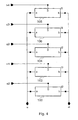
- the capacitor tuning block 40 comprises five binary weighted capacitor blocks 100, 102, 104, 106 and 108 arranged in parallel.
- Each capacitor block has its own select signal S0 to S4 which controls whether the capacitor within the respective block is switched into or removed from the circuit formed between the connections A and B in Figure 4 , which connect to nodes formed between the inductor 2 and transistor 4 on the one hand, and the node formed between the inductor 22 and the transistor 24 on the other hand in Figure 1 .
- a field effect transistor and capacitor are connected in series between the nodes A and B of the resonant circuit. Transistor acts merely as a switch in that it is driven to be either in a high impedance or a low impedance state in response to a control signal.
- Figure 4a illustrates the internal configuration of one of the capacitor blocks in greater detail.
- a capacitor 50, a field effect transistor 54 and a further capacitor 52 are connected in series between the nodes "A" and "B".
- both the source and drain of the field effect transistor 54 are connected via resistors 110 and 114 to the output of an inverter 112 which receives a "capacitor select" signal at its input.
- the output of the inverter 112 is also provided as an input to a further inverter 116 whose output is connected to a gate of the transistor 54 via a resistor 118.
- the circuit causes the transistor 54 to be switched hard on thereby minimising the on resistance for a given device size, whilst also allowing the device to be switched hard off, small devices are advantageous as they have reduced parasitic capacitance. Furthermore the circuit is completely balanced.
- the varactor 42 is of a known design and comprises two field effect transistors 60 and 62.
- a gate of the transistor 60 is connected to the drain 4 of the first field effect transistor 6 whereas a gate of the transistor 62 is connected to the drain 24 of the second field effect transistor 26.
- the drains and sources of the transistors 60 and 62 are connected together and also to a varactor control line 64.
- the voltage between the gate and the drain and source of each of the transistors 60 and 62 can be considered as effectively changing the dimensions between the insulated gate and the conducting channel (which is effectively one of the plates of the capacitor) within each of the transistors 60 and 62 thereby giving rise to the variation of the capacitance exhibited by the varactor 42.
- FIG. 2 schematically illustrates the response of the varactor.
- the abcissa represents the control voltage applied to the varactor which is the voltage between the gate and the source/drain of each of the transistors 60 and 62 (the sources and drains being coupled together).
- the ordinate of Figure 2 represents the capacitance of the varactor. It can be seen that as the control voltage rises from zero towards a first threshold VT1 the capacitance of the varactor remains essentially unchanged. The capacitance then rises steeply as the control voltage rises from VT1 towards VT2. For control voltages above VT2 the capacitance increases only very slowly with increasing control voltage.
- the voltages VT1 and VT2 are relatively close together and hence the varactor response can be considered as having an essentially digital response with a short transition region in the range VT1 to VT2.
- Figure 3a schematically illustrates the voltage occurring at the drain of one of the transistors 6 and 26 with respect to time. Also schematically illustrated on Figure 3a are two voltages 80 and 82 which represent differing control voltages applied on the varactor control line 64. However it will be appreciated that the varactor does not in fact respond solely to the voltage on its control line 64 but in fact responds to the voltage difference between the voltage on the control line 64 and the voltage at the gates of the transistors 60 and 62. Consequentially the varactor responds to the sum of the alternating voltage and the DC control voltage.
- the varactor can be turned on and off, as shown in Figures 3b and Figures 3c with the mark-space ratio between the on periods and the off periods being varied by changing the DC control voltage on the input line 64.
- Figure 3b shows the consequence of having a relatively low control voltage on the control line 64 such that the sum of the control voltage and the output voltage from the oscillator only exceeds the switching threshold for a relatively short period of time, that is when the voltage across the varactor's transistor exceeds the threshold represented by the chain line 80.
- gross frequency selection is determined by selecting or deselecting the various capacitors within the capacitor bank 40.
- the selection and deselection of such capacitors results in changes in the components contributing to the oscillator circuit, and this invariably leads to changes in the quality factor, Q, of the oscillator.
- Q quality factor
- This in part can be visualised as resistive losses within the switching transistor 54.
- These changes in quality factor give rise to changes in the amplitude of the oscillator output.
- Changes in the amplitude of the oscillator output give rise to variations in the time for which the voltage VGSD across the varactor exceeds the switching threshold and hence it becomes apparent that the frequency of the voltage controlled oscillator is dependant upon the amplitude of the output of the voltage controlled oscillator.
- the first limiting regime is a current limiting regime.
- the oscillator has a nominal switching frequency it follows that the rate of change of current is limited by the bias current supplied from the current source 10.
- the voltage waveform developed across the inductors 2 and 22 can be controlled by varying the current flowing through the current source 10.
- An alternative limiting regime is a voltage control regime which occurs because the current source 10 will, in reality, be built using transistors and these will require a minimum voltage head room across them in order to operate properly. Consequently, as the amplitude of oscillation increases the voltage head room across the current source 10 decreases. Eventually the head room across the current source 10 decreases to such an extent that it ceases to function correctly. This necessarily results in limitation of the voltage control oscillator output voltage.
- the peak to peak amplitude of the oscillation within the voltage control oscillator would be measured using a peak to peak detector and this voltage would be supplied to a first input of an error amplifier.
- the second input of the error amplifier would receive a reference voltage and the output of the error amplifier would be a function of a difference between the measured peak to peak voltage and the target peak to peak voltage.
- the output of the error amplifier is then provided to a control input of the variable current source 10 so as to stabilise the amplitude of oscillation of the VCO.
- digital control of the current source provides enhanced phase noise performance. This is because the periodic nature of digital control means that for the majority of the time that the current source is running, the current control signal to the current source is invariant.
- the unchanging nature of the current control signal means that the control signal does not become a source of noise in the current supplied by the current source and consequently does not get converted to phase noise by virtue of the action of the VCO.
- the changes in the bias current may be constrained to occur when the telephone is not engaged in transmitting and/or receiving.
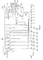
- FIG. 5 schematically shows an oscillator and level control circuit (which forms part of an oscillator controller) constituting an embodiment of the present invention.
- the oscillator generally indicated 200, is of the type described hereinbefore with reference to Figures 1 to 4 .
- Connections are made to nodes 202 and 204 representing the connection between inductor 2 and transistor 6 in a first side of the oscillator 200 and between inductor 22 and transistor 26 in a second side of the oscillator 200, respectively.
- the connections from nodes 202 and 204 extend, via decoupling capacitors 210 and 212 to first and second inputs of a rectifier 216 which rectifies the voltage difference to obtain a measure of the peak to peak amplitude of the output of the oscillator.
- An output 218 of the rectifier 216 is supplied via a low pass filter 220 to a non-inverting input 222 of a comparator 224.
- An inverting input 226 of the comparator 224 receives a reference input indicative of the target amplitude of the oscillator 200.
- An output of the comparator is provided to a level controller 230 which provides control signals to a plurality of digitally controllable current mirrors 240, 242, 244, 246 and 248 via a control bus 250. It will be appreciated that more current mirrors can be provided if desired.
- the current mirrors have a common structure and, for brevity, only the first current mirror 240 will be described in detail.
- the mirror 240 comprises a pair of matched transistors 260 and 262 whose gates are coupled together.
- the transistors 260 and 262 also have their source terminals coupled together and to the local ground connection 264.
- the drain terminal of the transistor 260 is connected to a supply rail 266 via an electrically controlled switch 268 and a current control resistor 270.
- the drain terminal of transistor 262 is connected to the oscillator 200, and more particularly to a node 272 at an input of an inductor 274 which in turn connects to a node 276 to which the sources of the transistors 6 and 26 are connected.
- the inductor 274 is beneficial as it presents a high impedance to oscillations propagating into the current mirror.
- the current mirrors have the same configuration, but the values of the current control resistors vary between the mirrors.
- the current mirrors are advantageously binary weighted. If mirror 240 is the most significant mirror, then if the resistor 270 in the mirror 240 has a value R, then the current control resistor in the next mirror has a value 2R, such that half the current flows in mirror 242 compared to that flowing in current mirror 240.
- the value of the current control resistor in the current mirror 246 is 4R, the value of the current control resistor in the next current mirror 248 is 8R, and so on.
- a further current mirror 280 is provided whose current is the minimum amount required to sustain operation of the oscillator (plus a margin of safety) and this current mirror 280 is permanently on.
- the supply rail 266 could be derived from a voltage reference, but advantageously is the voltage supply rail to the oscillator core 200.
- decoupling capacitor 282 plays a dual role, ensuring stability and limiting noise bandwidth at the LDO output (a function which is usually essential) and simultaneously limiting noise bandwidth in the bias generation circuits.
- the supply to the oscillator core may be via a low drop out voltage regulator (i.e. a regulator which does not require much voltage headroom) which may be of a relatively simple design.
- the regulator is advantageously not designed to maximise regulation but instead is designed to minimise noise. This improves phase noise performance of the oscillator.
- FIGs 6 and 7 show an embodiment of an oscillator in accordance with the present invention and as schematically shown in Figure 5 .
- the oscillator, generally labelled 200 corresponds functionally with the circuit shown in Figure 1 .
- the inductors 2 and 22 are implemented within functional block 302, coarse tuning is implemented by the switchable capacitors within the tuning block 40 and fine control is performed by the varactor 42.
- the cross coupled field effect transistors 6 and 26 receive current from a current mirror generally designated 306.
- the various transistors within the current mirror 306 are controlled by a switching circuit 308.
- the oscillator 200 it further includes a buffer circuit 310 which makes a buffered version of the output of the oscillator available for use in other parts of the telecommunication device.
- a detection tap circuit 312 which provides signals 316 and 318 representing the amplitude of oscillation.
- the outputs of the detector tap circuit 312 are provided to a further detection element 322, shown in Figure 7 , which serves to rectify and smooth the signals on lines 316 and 318 to produce a composite detected signal.
- the detection element 322 also receives a target amplitude from a controller 230 via input 330.
- the detection element compares the prevailing amplitude with the target value and outputs the result of the comparison to the non-inverting input of a comparator 224.
- the inverse of the comparison is provided to the inverting input of the comparator 224.
- the comparator 224 acts to scale and level shift the output of the detection element 320 such that a digital signal suitable for use by other digital circuits is obtained.
- the controller 230 can control the amplitude of the oscillator by virtue of the current mirror 10 ( Figure 1 ).
- the current mirror (shown in detail in Figure 6 ) comprises six digitally controllable binary weighted current mirrors 240, 242, 246, 248, 340, 342, together with one permanently on channel 280 which ensures that a minimum value current flow always exists. This is useful as it prevents the oscillator being turned off inadvertently.
- the GSM telephone mobile system is a time division multiple access, TDMA, system in which the mobile telephone only transmits or receives during predefined slots.
- TDMA time division multiple access
- the present invention can also be applied to code division multiple access, CDMA, systems, including 3G telephone systems, where the transmitters and receivers are continuously active.
- the application of the present invention to CDMA systems is appropriate because the periodic nature of digital systems means that the control word or signal to the current source, i.e., current mirror 10 is still only periodically updated and hence during the majority of a clock cycle the control signal/word is invariant and hence not a source of noise.
- amplitude correction need only be performed periodically. In fact, the amplitude correction could be performed once and only once at power up. However, for improved performance it would be expected that it would be repeated every now and again in order to account for temperature changes, for example because heat from the user's hand causes gradual warming of a mobile telephone.
- the mobile telephone may have to be frequency agile.
- the GSM telephone system may require the mobile telephone to change operating frequency during the telephone call. If the frequency change is instructed the telephone only has a period of about 200 ⁇ s to set its operating frequency before its next transmit cycle.
- the capacitors are switched in and out of the oscillator circuit to perform a successive approximation search of the frequency space.
- the most significant, that is largest, capacitor is switched into the circuit and the measurement of the oscillation frequency is made to determine whether the oscillator is higher or lower than the target frequency. If the oscillator is higher than the target frequency then the capacitor remains selected, otherwise it is switched back out of the oscillator circuit. Then the next most significant capacitor is switched into the oscillator circuit and again a frequency measurement is made to determine whether the oscillator frequency is higher or lower than the target frequency. If the oscillator is higher than the target frequency then the capacitor remains selected, otherwise it is removed from the circuit again. This process is repeated for each of the capacitors, it being borne in mind that the selection of each capacitor reduces the operating frequency.
- the inventors Due to the interrelation of the amplitude and oscillating frequency, the inventors have realised that it is appropriate to interleave amplitude stabilisation with the capacitor frequency search. This is achieved by integrating the tests such that once the first capacitor is switched into the circuit, an amplitude test and stabilisation is performed prior to making the frequency measurements and frequency decision. Indeed, the process can be extended such that once the first capacitor is selected, selection or initiation of the second capacitor test causes the amplitude control to be performed again before the frequency measurement step associated with the second capacitor is performed. The process can also be repeated in respect of the third and subsequent capacitors although it could reasonably be expected that as the capacitor selection moves from the most significant to the least significant capacitor, amplitude variation associated with this process will also reduce. Thus the designer has an option to inhibit the amplitude stabilisation for the least significant capacitors if so desired.
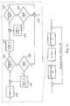
- FIG 8 is a block diagram schematically illustrating the frequency or band selection and level control procedure as implemented within a mobile telephone constituting an embodiment of the present invention.
- a controller (not shown) handles the processing of control signals with the mobile telephone infrastructure.
- the controller has already received and decoded instructions concerning what frequencies the telephone is to receive and transmit on.
- step 400 commences at step 400 where a new frequency word is loaded. This word represents the target frequency of the voltage controlled oscillator. Control then passes to step 402 where the VCO calibration is performed. Once this has been completed control is passed to step 404 where, a transmit or receive operation is performed. From step 404 control can pass to other procedures (not shown) or can be directed by the controller to return to step 400.
- Step 402 is in fact an iterative step which itself causes several steps to be performed. Sub-steps to step 402 are schematically illustrated within the outlined box 406 in Figure 8 .
- the VCO calibration involves a successive approximation search through frequency space to lock the oscillator to a frequency band which includes the desired frequency.
- the coarse tuning of the oscillator is controlled by the switching of binary weighted capacitors (although binary weighting is not essential). Fine control can be performed using the varactor. During the frequency selection the varactor is set to its minimum capacitance value. This has the consequence that the varactor can only be used to fine tune the oscillator's frequency is a downwards direction. Other modes are possible, for example the varactor could be set to its maximum capacitance and hence fine frequency control would be in the direction of increasing frequency.
- Figure 9 shows how the operating frequency varies with the capacitance control word and varactor voltage.
- the capacitance control word is set to 0 corresponding to its minimum value and with all capacitors nominally switched out of the oscillator, then the oscillator will oscillate at its highest frequency.
- the control word is increased sequentially towards its maximum value N, then the 1st, 2nd ... to Nth bands are selected, each having a lower initial frequency than the preceding band. It is important for frequency coverage that the bands overlap with at least the nearest adjacent band so as to ensure that there are no gaps in the operating range between the minimum and maximum frequencies that have to be produced.
- tuning bands there are 64 tuning bands, labelled 0 to 63, available. Those can be selected via a 6 bit control word. If we assume that the least significant bit is bit 0, and the most significant bit is bit 5, then the VCO set up procedure performs the frequency search as follows.
- the frequency select bits are successively tested from bit 5 to bit 0 by repeatedly running steps 410, 412 and 414 ( Figure 8 ).
- step 410 the bit under test of the frequency control word is set. During the first pass through this test this is bit 5. Control is then passed to step 412 where amplitude level control is performed. Once the oscillator amplitude has been set control is passed to step 414 where is a comparison of the oscillator frequency is made with the target frequency as defined by the frequency control word which was loaded at step 400. The comparison is made by measuring the oscillator against a reference frequency provided from a crystal oscillator.
- next most significant bit is selected and steps 410, 412 and 414 are repeated.
- steps 410, 412 and 414 are repeated.
- the correct frequency band has been located.
- LSB last frequency control bit
- a further amplitude level control cycle might be run to adjust amplitude for the actual band which has been selected.
- Oscillator control is then passed to the phase locked loop which locks on to the target frequency and makes fine adjustments of the oscillator frequency via the varactor control voltage.
- Figure 10 schematically illustrates the processes performed within step 412 of Figure 9 .
- TGT1 and TGT2 are employed during the coarse and fine phases of the search respectively.
- the value of TGT1 is constrained to be less the maximum safe amplitude minus the maximum expected coarse step size.
- TGT2 is set equal to the value of the required amplitude minus the equivalent of 1 ⁇ 2 of the least significant bit.
- step 420 The algorithm commences at step 420 where "level" is set to an initial value of three. Control is then passed to step 422 where a comparison of the oscillator amplitude is made with a first target value TGT1. A comparison is made at step 422, and if the value of the oscillator amplitude exceeds the first target TGT1, then control is passed to step 424. However, if the value of the oscillator amplitude is still less than TGT1 control passes to step 426 where a test is made on the value of "level”. If the value of "level” is less than 63 control is passed to step 428 where the value of "level” is increased by four and control is then returned to step 422. However if the test at step 426 determines that the value of "level” is not less than 63, control is then passed to step 440 which represents an exit from the amplitude control routine.
- step 424 acts to decrement the value of "level” by three.
- Control is then passed to step 432 where the oscillator amplitude is compared with the second target, TGT2.
- the value of the second target TGT2 is set to the required amplitude of the oscillator minus one half the value of the least significant bit of the level control. If step 432 determines that the amplitude is greater than the value TGT2 then control is passed to step 440 which represents the exit from the level setting routine. However if step 432 determines that the oscillator amplitude is less than TGT2 then control is passed to step 434. Step 434 tests the value of "level” and if it is less than 63 then control is passed to step 430, otherwise control is passed to step 440. At step 430 the value of "level” is incremented by one. Control is then passed to step 432.
- FIGs 11 and 12 schematically illustrate circuits which are suitable for determining the frequency of oscillation of the oscillator shown in Figure 1 .
- the telephone can be instructed to set its oscillator to any one of a predetermined series of frequencies.
- the frequencies are not randomly chosen, but in fact are pre-allocated channel frequencies.
- Each GSM telephone is provided with a highly accurate oscillator which forms a frequency and timing reference for the telephone.
- the oscillator controller comprises two counters 500 and 502 which are of an identical construction.
- the first counter 500 receives the frequency reference signal Fref at a clock input and divides the frequency signal by a predetermined number, for example 32. At the end of this division an output 506 of the counter 500 will change state, for example by going to a logical high.
- the counter 502 is connected to the voltage controlled oscillator 510 via a fractional divider 512.
- the target VCO frequency is a multiple of the frequency reference. This multiple of the frequency reference is designated N.
- the fractional divider 512 is programmed to divide by N then the signal provided to the second counter 512 should be at the same frequency as that provided to the first counter 500.
- the output 506 of the first counter 500 is provided to a first input 514 of a controller 516.
- An output 520 of the second counter 502 is provided to a second input 522 of the controller 516.
- the controller 516 can reset the counters 500 and 502, or allow them to start counting via a shared control line 524.
- the reset/control line 524 may go low to reset the counters, and may be sent high to initiate the count. If the signal is received from the counter 502 before the counter 500 then an output 524 asserting that the voltage control oscillator is running faster than the reference can be asserted.
- Figure 12 shows the circuit configuration for performing the fine frequency control of the voltage controlled oscillator 510.
- the output of the VCO is divided down by the fractional divider 512.
- a phase-frequency sensitive detector 530 is provided which receives the frequency reference signal at a first input thereof and the output of the fractional divider 512 at a second input thereof.
- the phase-frequency sensitive detector which is a well known component, produces an output 531 representative of the phase difference between its input signals. This signal, whose polarity and magnitude represents the correction to be applied to the voltage controlled oscillator, is supplied to a first input of a charge pump 536.
- a correction calculator 534 is responsive to a frequency control word from the controller and outputs a correction value to a second input controlling a bias current of the charge pump 536.
- the output of the charge pump is low pass filtered and used to control the varactor 42 in the voltage controlled oscillator 510.
- the correction calculator 534 can advantageously be implemented as a lookup table as this allows the degree of resolution and the shape of the function that the correction calculator implements to be varied at the designer's will.
- the correction calculator will implement a function that varies as frequency squared in order to compensate for the fact that the change in frequency with respect to the change in capacitance varies as the frequency cubed.
- a switch 540 is provided at the input to the VCO.
- the switch can be selected so as to connect the input of the voltage controlled oscillator to a reference voltage 542 in order to maintain the varactor frequency control at a predetermined value.
Landscapes
- Inductance-Capacitance Distribution Constants And Capacitance-Resistance Oscillators (AREA)
- Stabilization Of Oscillater, Synchronisation, Frequency Synthesizers (AREA)
Applications Claiming Priority (2)
| Application Number | Priority Date | Filing Date | Title |
|---|---|---|---|
| US10/679,997 US7038552B2 (en) | 2003-10-07 | 2003-10-07 | Voltage controlled oscillator having improved phase noise |
| EP04785330A EP1673855B1 (de) | 2003-10-07 | 2004-09-30 | Spannungsgesteuerter oszillator mit verbessertem phasenrauschen |
Related Parent Applications (1)
| Application Number | Title | Priority Date | Filing Date |
|---|---|---|---|
| EP04785330.4 Division | 2004-09-30 |
Publications (2)
| Publication Number | Publication Date |
|---|---|
| EP2278702A2 true EP2278702A2 (de) | 2011-01-26 |
| EP2278702A3 EP2278702A3 (de) | 2012-12-19 |
Family
ID=34394290
Family Applications (2)
| Application Number | Title | Priority Date | Filing Date |
|---|---|---|---|
| EP10184041A Withdrawn EP2278702A3 (de) | 2003-10-07 | 2004-09-30 | Spannungsgesteuerter Oszillator mit verbessertem Phasenrauschen |
| EP04785330A Expired - Lifetime EP1673855B1 (de) | 2003-10-07 | 2004-09-30 | Spannungsgesteuerter oszillator mit verbessertem phasenrauschen |
Family Applications After (1)
| Application Number | Title | Priority Date | Filing Date |
|---|---|---|---|
| EP04785330A Expired - Lifetime EP1673855B1 (de) | 2003-10-07 | 2004-09-30 | Spannungsgesteuerter oszillator mit verbessertem phasenrauschen |
Country Status (5)
| Country | Link |
|---|---|
| US (2) | US7038552B2 (de) |
| EP (2) | EP2278702A3 (de) |
| CN (2) | CN102638224B (de) |
| TW (1) | TWI411235B (de) |
| WO (1) | WO2005039038A2 (de) |
Cited By (2)
| Publication number | Priority date | Publication date | Assignee | Title |
|---|---|---|---|---|
| TWI427933B (zh) * | 2011-03-18 | 2014-02-21 | Realtek Semiconductor Corp | 鎖相迴路及其方法 |
| CN117081587A (zh) * | 2023-10-16 | 2023-11-17 | 深圳市九天睿芯科技有限公司 | 一种锁相环、芯片及电子设备 |
Families Citing this family (80)
| Publication number | Priority date | Publication date | Assignee | Title |
|---|---|---|---|---|
| GB2389254B (en) * | 2002-05-31 | 2005-09-07 | Hitachi Ltd | Semiconductor integrated circuit device for communication |
| US8243876B2 (en) | 2003-04-25 | 2012-08-14 | Rapiscan Systems, Inc. | X-ray scanners |
| US8451974B2 (en) | 2003-04-25 | 2013-05-28 | Rapiscan Systems, Inc. | X-ray tomographic inspection system for the identification of specific target items |
| US9113839B2 (en) | 2003-04-25 | 2015-08-25 | Rapiscon Systems, Inc. | X-ray inspection system and method |
| US8837669B2 (en) | 2003-04-25 | 2014-09-16 | Rapiscan Systems, Inc. | X-ray scanning system |
| GB0525593D0 (en) | 2005-12-16 | 2006-01-25 | Cxr Ltd | X-ray tomography inspection systems |
| US7949101B2 (en) | 2005-12-16 | 2011-05-24 | Rapiscan Systems, Inc. | X-ray scanners and X-ray sources therefor |
| US20050058242A1 (en) | 2003-09-15 | 2005-03-17 | Peschmann Kristian R. | Methods and systems for the rapid detection of concealed objects |
| DE602004011769T2 (de) * | 2003-06-27 | 2009-02-05 | Matsushita Electric Industrial Co., Ltd., Kadoma-shi | Vco-einrichtung |
| US20060145776A1 (en) * | 2005-01-05 | 2006-07-06 | Qian Shi | High-speed VCO calibration technique for frequency synthesizers |
| JP4190503B2 (ja) * | 2005-01-20 | 2008-12-03 | 富士通マイクロエレクトロニクス株式会社 | 電圧制御発振回路、およびその調整方法 |
| US7342465B2 (en) * | 2005-10-20 | 2008-03-11 | Honeywell International Inc. | Voltage-controlled oscillator with stable gain over a wide frequency range |
| US7330079B2 (en) * | 2005-10-31 | 2008-02-12 | Texas Instruments Incorporated | Method and apparatus for rapid local oscillator frequency calibration |
| US7439817B2 (en) * | 2006-02-16 | 2008-10-21 | Texas Instruments Incorporated | Frequency tuning range extension and modulation resolution enhancement of a digitally controlled oscillator |
| US7852408B2 (en) * | 2006-05-16 | 2010-12-14 | Lsi Corporation | Fractional phase-locked loop for generating high-definition and standard-definition reference clocks |
| TWI323565B (en) * | 2006-06-16 | 2010-04-11 | Realtek Semiconductor Corp | Voltage-controlled oscillator |
| DE102006032276B4 (de) * | 2006-07-12 | 2011-10-27 | Infineon Technologies Ag | Amplitudenregelungsschaltung |
| US7425909B2 (en) * | 2006-07-31 | 2008-09-16 | Analog Devices, Inc. | Low-noise programmable current source |
| US7548120B2 (en) * | 2006-08-09 | 2009-06-16 | Mstar Semiconductor, Inc. | Frequency switching method |
| US7661007B2 (en) * | 2006-09-28 | 2010-02-09 | Via Technologies, Inc. | Methods and systems for adjusting clock frequency |
| US7920033B1 (en) * | 2006-09-28 | 2011-04-05 | Groe John B | Systems and methods for frequency modulation adjustment |
| TWI321909B (en) * | 2006-11-17 | 2010-03-11 | Sunplus Technology Co Ltd | Switch capacitance and varactor bank applied to voltage controlled oscillator having constant kvco |
| CN100578913C (zh) * | 2006-12-21 | 2010-01-06 | 凌阳科技股份有限公司 | 一种使用于压控振荡器中的一可变电容器 |
| US7592878B2 (en) * | 2007-04-05 | 2009-09-22 | Qualcomm Incorporated | Method and apparatus for generating oscillating signals |
| JP2008306331A (ja) * | 2007-06-06 | 2008-12-18 | Toshiba Corp | 半導体集積回路装置 |
| US20090003503A1 (en) * | 2007-06-29 | 2009-01-01 | Rotem Banin | Frequency detector for VCO band selection |
| US7728676B2 (en) | 2007-09-17 | 2010-06-01 | Atheros Communications, Inc. | Voltage-controlled oscillator with control range limiter |
| CN101409530B (zh) * | 2007-10-12 | 2012-03-21 | 瑞昱半导体股份有限公司 | 压控振荡器 |
| US8019564B2 (en) * | 2008-01-07 | 2011-09-13 | Qualcomm Incorporated | Systems and methods for calibrating the loop bandwidth of a phase-locked loop (PLL) |
| US20090189699A1 (en) * | 2008-01-29 | 2009-07-30 | Broadcom Corporation | Fixed bandwidth lo-gen |
| US8674771B2 (en) * | 2008-01-29 | 2014-03-18 | Broadcom Corporation | Fixed bandwidth LO-GEN |
| US7728631B2 (en) * | 2008-05-15 | 2010-06-01 | Atheros Communications, Inc. | Phase frequency detector with pulse width control circuitry |
| JP5195652B2 (ja) * | 2008-06-11 | 2013-05-08 | ソニー株式会社 | 信号処理装置、および信号処理方法、並びにプログラム |
| JP2010056856A (ja) * | 2008-08-28 | 2010-03-11 | Renesas Technology Corp | 半導体集積回路 |
| US9310323B2 (en) | 2009-05-16 | 2016-04-12 | Rapiscan Systems, Inc. | Systems and methods for high-Z threat alarm resolution |
| US8044739B2 (en) | 2009-06-09 | 2011-10-25 | Qualcomm Incorporated | Capacitor switching circuit |
| JP2011259192A (ja) * | 2010-06-09 | 2011-12-22 | Sony Corp | マルチバイブレータ回路および電圧変換回路 |
| US8275336B2 (en) * | 2010-06-23 | 2012-09-25 | Richwave Technology Corp. | Apparatus and method for digitally controlling capacitance |
| US20120074998A1 (en) | 2010-09-27 | 2012-03-29 | Stephen Jonathan Brett | Integrated circuit device, electronic device and method for compensating frequency drift of a controllable oscillator |
| JP2012134615A (ja) * | 2010-12-20 | 2012-07-12 | Ricoh Co Ltd | 発振装置および該発振装置を具備したクロック発生装置、半導体装置、ならびに電子装置 |
| EP2482459A1 (de) * | 2011-01-28 | 2012-08-01 | Nxp B.V. | Oszillatoramplitudensteuerung |
| US9099956B2 (en) | 2011-04-26 | 2015-08-04 | King Abdulaziz City For Science And Technology | Injection locking based power amplifier |
| US20120286888A1 (en) * | 2011-05-09 | 2012-11-15 | Taiwan Semiconductor Manufacturing Company, Ltd. | Switched Capacitor Array for Voltage Controlled Oscillator |
| US8493040B2 (en) * | 2011-08-04 | 2013-07-23 | Nxp B.V. | Voltage regulator with charge pump |
| US8593227B2 (en) | 2011-08-05 | 2013-11-26 | Qualcomm Incorporated | System and method of controlling gain of an oscillator |
| US8884718B2 (en) * | 2011-08-09 | 2014-11-11 | Si-Ware Systems | Method and apparatus to control the LC tank temperature null characteristic in a highly stable LC oscillator |
| US9350321B2 (en) | 2011-08-18 | 2016-05-24 | Analog Devices, Inc. | Low distortion impedance selection and tunable impedance circuits |
| JP5863395B2 (ja) * | 2011-11-02 | 2016-02-16 | 日本電波工業株式会社 | 発振器 |
| US9823383B2 (en) | 2013-01-07 | 2017-11-21 | Rapiscan Systems, Inc. | X-ray scanner with partial energy discriminating detector array |
| US10459784B2 (en) | 2013-06-28 | 2019-10-29 | Infineon Technologies Ag | Frequency signal generator, a frequency modulated continuous wave radar system and a method for generating a frequency signal |
| KR20150054506A (ko) | 2013-11-12 | 2015-05-20 | 삼성전자주식회사 | 전자 장치에서 전압 제어 오실레이터의 출력 진폭 제어 장치 및 방법 |
| US9557427B2 (en) | 2014-01-08 | 2017-01-31 | Rapiscan Systems, Inc. | Thin gap chamber neutron detectors |
| KR102204174B1 (ko) * | 2014-01-13 | 2021-01-18 | 한국전자통신연구원 | 전하 펌프 회로 및 이를 포함하는 위상 고정 루프 |
| US8942315B1 (en) * | 2014-05-29 | 2015-01-27 | Cypress Semiconductor Corporation | Systems, methods, and devices for frequency calibration of transmitters |
| CN107210767B (zh) * | 2015-02-04 | 2018-10-26 | 谷歌有限责任公司 | 具有本地振荡器调制的无线电接收器 |
| US9473151B1 (en) | 2015-06-05 | 2016-10-18 | Telefonaktiebolaget Lm Ericsson (Publ) | Low-noise oscillator amplitude regulator |
| US10345479B2 (en) | 2015-09-16 | 2019-07-09 | Rapiscan Systems, Inc. | Portable X-ray scanner |
| CN107017837B (zh) * | 2015-10-27 | 2022-02-08 | 精工爱普生株式会社 | 电路装置、振荡器、电子设备以及移动体 |
| US10419005B2 (en) * | 2016-12-14 | 2019-09-17 | Taiwan Semiconductor Manufacturing Co., Ltd. | Phase-locked-loop architecture |
| US10454418B1 (en) * | 2017-02-14 | 2019-10-22 | Xilinx, Inc. | Voltage-controlled oscillator with high and low gain options |
| US10826429B2 (en) | 2017-11-29 | 2020-11-03 | Mediatek Inc. | Compensation module, oscillation circuit, and associated compensation method capable of reducing sensitivity of output oscillation signal |
| CN107979371B (zh) * | 2017-12-28 | 2024-03-22 | 上海先基半导体科技有限公司 | 一种锁相环及其压控振荡器 |
| CN108233923B (zh) * | 2018-01-09 | 2021-09-14 | 上海顺久电子科技有限公司 | Vco及其频率校准方法、电子设备及计算机存储介质 |
| CN108649902B (zh) * | 2018-05-14 | 2024-01-23 | 成都中宇微芯科技有限公司 | 一种温度补偿压控振荡器及补偿方法 |
| US10778235B2 (en) * | 2018-10-28 | 2020-09-15 | Nuvoton Technology Corporation | Intermittent tuning of an oscillator |
| CN109660253B (zh) * | 2018-11-05 | 2022-11-25 | 西安电子科技大学 | 一种数字振幅控制的压控振荡器 |
| US10491226B1 (en) * | 2018-12-27 | 2019-11-26 | Audiowise Technology Inc. | Method, processing circuit, and wireless communication device capable of tuning current provided for DCO to lower current level as far as possible |
| US10862425B2 (en) * | 2019-04-25 | 2020-12-08 | Shenzhen GOODIX Technology Co., Ltd. | Differential switchable capacitors for radiofrequency power amplifiers |
| CN110620552A (zh) * | 2019-08-30 | 2019-12-27 | 苏州闻颂智能科技有限公司 | 一种基于电容补偿技术的线性压控振荡器 |
| US11152890B2 (en) | 2020-02-25 | 2021-10-19 | International Business Machines Corporation | Low power oscillator with digital amplitude control |
| JP6886544B1 (ja) | 2020-04-20 | 2021-06-16 | ウィンボンド エレクトロニクス コーポレーション | 発振回路 |
| FR3113519B1 (fr) | 2020-08-24 | 2022-09-02 | Commissariat Energie Atomique | Procédé de mesure d’un champ magnétique extérieur par au moins un point mémoire magnétique |
| EP3992748A1 (de) * | 2020-11-03 | 2022-05-04 | pSemi Corporation | Ldo mit selbstkalibrierender kompensation von resonanzeffekten |
| US11418204B2 (en) * | 2020-12-22 | 2022-08-16 | Stmicroelectronics International N.V. | Phase lock loop (PLL) with operating parameter calibration circuit and method |
| CN113315357B (zh) * | 2021-04-20 | 2022-06-14 | 山东奥太电气有限公司 | 一种大功率逆变电源错相控制系统及方法 |
| US12206361B2 (en) * | 2021-12-15 | 2025-01-21 | Texas Instruments Incorporated | Oscillator frequency accuracy and amplitude control |
| CN114356011B (zh) * | 2021-12-28 | 2024-02-27 | 京微齐力(北京)科技有限公司 | 低压差线性稳压器电路 |
| CN116449900A (zh) * | 2022-01-17 | 2023-07-18 | 联发科技(新加坡)私人有限公司 | 电压调节器 |
| JP2024129361A (ja) * | 2023-03-13 | 2024-09-27 | セイコーエプソン株式会社 | 回路装置および発振器 |
| CN117054847B (zh) * | 2023-07-31 | 2024-04-19 | 中国矿业大学 | 一种评估vco相位噪声灵敏度的方法 |
Family Cites Families (15)
| Publication number | Priority date | Publication date | Assignee | Title |
|---|---|---|---|---|
| JP2845185B2 (ja) * | 1995-11-29 | 1999-01-13 | 日本電気株式会社 | Pll回路 |
| JPH1168560A (ja) * | 1997-08-20 | 1999-03-09 | Nec Corp | Pll周波数シンセサイザおよびチャージポンプ回路 |
| JP3360667B2 (ja) * | 1999-12-01 | 2002-12-24 | 日本電気株式会社 | 位相同期ループの同期方法、位相同期ループ及び該位相同期ループを備えた半導体装置 |
| JP4094851B2 (ja) * | 2000-01-17 | 2008-06-04 | 富士通株式会社 | Pll回路 |
| SE518113C2 (sv) * | 2000-03-06 | 2002-08-27 | Ericsson Telefon Ab L M | Metod och anordning för att förbättra strömstyrande D/A- omvandling |
| JP2002076992A (ja) * | 2000-09-05 | 2002-03-15 | Nec Corp | 周波数調整回路 |
| US6552618B2 (en) * | 2000-12-13 | 2003-04-22 | Agere Systems Inc. | VCO gain self-calibration for low voltage phase lock-loop applications |
| JP3414382B2 (ja) * | 2001-01-09 | 2003-06-09 | 日本電気株式会社 | Pll回路及びその制御方法 |
| US6583675B2 (en) * | 2001-03-20 | 2003-06-24 | Broadcom Corporation | Apparatus and method for phase lock loop gain control using unit current sources |
| US6483391B1 (en) * | 2001-03-30 | 2002-11-19 | Conexant Systems, Inc. | System for controlling the amplitude of an oscillator |
| US6680655B2 (en) | 2001-08-01 | 2004-01-20 | Sige Semiconductor Inc. | Automatic gain control for a voltage controlled oscillator |
| GB2384927A (en) | 2002-02-05 | 2003-08-06 | Zarlink Semiconductor Ltd | Voltage controlled oscillators |
| US7062229B2 (en) * | 2002-03-06 | 2006-06-13 | Qualcomm Incorporated | Discrete amplitude calibration of oscillators in frequency synthesizers |
| US6856791B2 (en) * | 2002-03-14 | 2005-02-15 | Ericsson Inc. | Direct automatic frequency control method and apparatus |
| US6608511B1 (en) * | 2002-07-17 | 2003-08-19 | Via Technologies, Inc. | Charge-pump phase-locked loop circuit with charge calibration |
-
2003
- 2003-10-07 US US10/679,997 patent/US7038552B2/en not_active Expired - Lifetime
-
2004
- 2004-09-30 WO PCT/US2004/032274 patent/WO2005039038A2/en not_active Ceased
- 2004-09-30 EP EP10184041A patent/EP2278702A3/de not_active Withdrawn
- 2004-09-30 EP EP04785330A patent/EP1673855B1/de not_active Expired - Lifetime
- 2004-09-30 CN CN201210114621.3A patent/CN102638224B/zh not_active Expired - Lifetime
- 2004-09-30 CN CNA2004800330788A patent/CN1879290A/zh active Pending
- 2004-10-05 TW TW093130101A patent/TWI411235B/zh not_active IP Right Cessation
-
2006
- 2006-02-27 US US11/362,935 patent/US7492228B2/en not_active Expired - Lifetime
Non-Patent Citations (1)
| Title |
|---|
| None |
Cited By (3)
| Publication number | Priority date | Publication date | Assignee | Title |
|---|---|---|---|---|
| TWI427933B (zh) * | 2011-03-18 | 2014-02-21 | Realtek Semiconductor Corp | 鎖相迴路及其方法 |
| CN117081587A (zh) * | 2023-10-16 | 2023-11-17 | 深圳市九天睿芯科技有限公司 | 一种锁相环、芯片及电子设备 |
| CN117081587B (zh) * | 2023-10-16 | 2024-03-26 | 深圳市九天睿芯科技有限公司 | 一种锁相环、芯片及电子设备 |
Also Published As
| Publication number | Publication date |
|---|---|
| CN1879290A (zh) | 2006-12-13 |
| EP2278702A3 (de) | 2012-12-19 |
| EP1673855B1 (de) | 2012-12-19 |
| WO2005039038A2 (en) | 2005-04-28 |
| US20050073371A1 (en) | 2005-04-07 |
| TWI411235B (zh) | 2013-10-01 |
| WO2005039038A3 (en) | 2005-07-07 |
| US7492228B2 (en) | 2009-02-17 |
| CN102638224B (zh) | 2014-10-29 |
| US20060145771A1 (en) | 2006-07-06 |
| TW200516859A (en) | 2005-05-16 |
| CN102638224A (zh) | 2012-08-15 |
| US7038552B2 (en) | 2006-05-02 |
| EP1673855A2 (de) | 2006-06-28 |
Similar Documents
| Publication | Publication Date | Title |
|---|---|---|
| US7038552B2 (en) | Voltage controlled oscillator having improved phase noise | |
| US6838951B1 (en) | Frequency synthesizer having VCO bias current compensation | |
| US6552618B2 (en) | VCO gain self-calibration for low voltage phase lock-loop applications | |
| KR100682279B1 (ko) | 주파수 합성기의 적응 주파수 조정장치 | |
| US9042854B2 (en) | Apparatus and methods for tuning a voltage controlled oscillator | |
| US6140882A (en) | Phase lock loop enabling smooth loop bandwidth switching | |
| US8149065B1 (en) | Low KVCO phase-locked loop with large frequency drift handling capability | |
| EP1982410B1 (de) | Oszillatorverstärkungsentzerrung | |
| US7609122B2 (en) | Method and system for calibration of a tank circuit in a phase lock loop | |
| JP2007525108A (ja) | 電圧制御デジタルアナログ発振器およびこれを用いた周波数シンセサイザ | |
| US7646253B2 (en) | Frequency-locked clock generator | |
| US20170040943A1 (en) | Electronic device with capacitor bank linearization and a linearization method | |
| US20220038105A1 (en) | Charge pump phase locked loop with low controlled oscillator gain | |
| EP1198879A1 (de) | Variabler oszillator | |
| US7010285B2 (en) | Phase locking loop frequency synthesizer | |
| KR100723838B1 (ko) | 주파수 합성 장치 | |
| US7650119B2 (en) | Wireless communication system and method using digital calibration to control mixer input swing | |
| JPH11251902A (ja) | Pll回路 | |
| US12362707B2 (en) | Device and method for signal synthesis compensating the frequency offset of open loop | |
| US20260066907A1 (en) | Phase-locked loop working system | |
| KR100664867B1 (ko) | 전압제어 발진기 | |
| EP1638207B1 (de) | Methode zum Kalibrieren der Frequenz eines Oszillators in einer Phasenregelschleife | |
| CN101019324A (zh) | 补偿高速pll电路 |
Legal Events
| Date | Code | Title | Description |
|---|---|---|---|
| PUAI | Public reference made under article 153(3) epc to a published international application that has entered the european phase |
Free format text: ORIGINAL CODE: 0009012 |
|
| AC | Divisional application: reference to earlier application |
Ref document number: 1673855 Country of ref document: EP Kind code of ref document: P |
|
| AK | Designated contracting states |
Kind code of ref document: A2 Designated state(s): DE FR GB |
|
| RIN1 | Information on inventor provided before grant (corrected) |
Inventor name: JONES, CHRISTOPHER GERAINT Inventor name: BRETT, STEPHEN JONATHAN Inventor name: FOWERS, PAUL Inventor name: STRANGE, JONATHAN RICHARD |
|
| RIN1 | Information on inventor provided before grant (corrected) |
Inventor name: STRANGE, JONATHAN RICHARD |
|
| PUAL | Search report despatched |
Free format text: ORIGINAL CODE: 0009013 |
|
| AK | Designated contracting states |
Kind code of ref document: A3 Designated state(s): DE FR GB |
|
| RIC1 | Information provided on ipc code assigned before grant |
Ipc: H03L 7/099 20060101AFI20121109BHEP |
|
| 17P | Request for examination filed |
Effective date: 20130426 |
|
| 17Q | First examination report despatched |
Effective date: 20160304 |
|
| STAA | Information on the status of an ep patent application or granted ep patent |
Free format text: STATUS: THE APPLICATION IS DEEMED TO BE WITHDRAWN |
|
| 18D | Application deemed to be withdrawn |
Effective date: 20160715 |