EP2259308A1 - Substrate for power module with heat sink and method for producing the same, power module with heat sink, and substrate for power module - Google Patents
Substrate for power module with heat sink and method for producing the same, power module with heat sink, and substrate for power module Download PDFInfo
- Publication number
- EP2259308A1 EP2259308A1 EP09721361A EP09721361A EP2259308A1 EP 2259308 A1 EP2259308 A1 EP 2259308A1 EP 09721361 A EP09721361 A EP 09721361A EP 09721361 A EP09721361 A EP 09721361A EP 2259308 A1 EP2259308 A1 EP 2259308A1
- Authority
- EP
- European Patent Office
- Prior art keywords
- power module
- heatsink
- metal layer
- module substrate
- face
- Prior art date
- Legal status (The legal status is an assumption and is not a legal conclusion. Google has not performed a legal analysis and makes no representation as to the accuracy of the status listed.)
- Granted
Links
Images
Classifications
-
- H—ELECTRICITY
- H10—SEMICONDUCTOR DEVICES; ELECTRIC SOLID-STATE DEVICES NOT OTHERWISE PROVIDED FOR
- H10W—GENERIC PACKAGES, INTERCONNECTIONS, CONNECTORS OR OTHER CONSTRUCTIONAL DETAILS OF DEVICES COVERED BY CLASS H10
- H10W40/00—Arrangements for thermal protection or thermal control
- H10W40/20—Arrangements for cooling
- H10W40/25—Arrangements for cooling characterised by their materials
- H10W40/255—Arrangements for cooling characterised by their materials having a laminate or multilayered structure, e.g. direct bond copper [DBC] ceramic substrates
-
- C—CHEMISTRY; METALLURGY
- C04—CEMENTS; CONCRETE; ARTIFICIAL STONE; CERAMICS; REFRACTORIES
- C04B—LIME, MAGNESIA; SLAG; CEMENTS; COMPOSITIONS THEREOF, e.g. MORTARS, CONCRETE OR LIKE BUILDING MATERIALS; ARTIFICIAL STONE; CERAMICS; REFRACTORIES; TREATMENT OF NATURAL STONE
- C04B37/00—Joining burned ceramic articles with other burned ceramic articles or other articles by heating
- C04B37/02—Joining burned ceramic articles with other burned ceramic articles or other articles by heating with metallic articles
- C04B37/021—Joining burned ceramic articles with other burned ceramic articles or other articles by heating with metallic articles in a direct manner, e.g. direct copper bonding [DCB]
-
- C—CHEMISTRY; METALLURGY
- C04—CEMENTS; CONCRETE; ARTIFICIAL STONE; CERAMICS; REFRACTORIES
- C04B—LIME, MAGNESIA; SLAG; CEMENTS; COMPOSITIONS THEREOF, e.g. MORTARS, CONCRETE OR LIKE BUILDING MATERIALS; ARTIFICIAL STONE; CERAMICS; REFRACTORIES; TREATMENT OF NATURAL STONE
- C04B2237/00—Aspects relating to ceramic laminates or to joining of ceramic articles with other articles by heating
- C04B2237/30—Composition of layers of ceramic laminates or of ceramic or metallic articles to be joined by heating, e.g. Si substrates
- C04B2237/32—Ceramic
- C04B2237/36—Non-oxidic
- C04B2237/366—Aluminium nitride
-
- C—CHEMISTRY; METALLURGY
- C04—CEMENTS; CONCRETE; ARTIFICIAL STONE; CERAMICS; REFRACTORIES
- C04B—LIME, MAGNESIA; SLAG; CEMENTS; COMPOSITIONS THEREOF, e.g. MORTARS, CONCRETE OR LIKE BUILDING MATERIALS; ARTIFICIAL STONE; CERAMICS; REFRACTORIES; TREATMENT OF NATURAL STONE
- C04B2237/00—Aspects relating to ceramic laminates or to joining of ceramic articles with other articles by heating
- C04B2237/30—Composition of layers of ceramic laminates or of ceramic or metallic articles to be joined by heating, e.g. Si substrates
- C04B2237/40—Metallic
- C04B2237/402—Aluminium
-
- C—CHEMISTRY; METALLURGY
- C04—CEMENTS; CONCRETE; ARTIFICIAL STONE; CERAMICS; REFRACTORIES
- C04B—LIME, MAGNESIA; SLAG; CEMENTS; COMPOSITIONS THEREOF, e.g. MORTARS, CONCRETE OR LIKE BUILDING MATERIALS; ARTIFICIAL STONE; CERAMICS; REFRACTORIES; TREATMENT OF NATURAL STONE
- C04B2237/00—Aspects relating to ceramic laminates or to joining of ceramic articles with other articles by heating
- C04B2237/50—Processing aspects relating to ceramic laminates or to the joining of ceramic articles with other articles by heating
- C04B2237/66—Forming laminates or joined articles showing high dimensional accuracy, e.g. indicated by the warpage
-
- C—CHEMISTRY; METALLURGY
- C04—CEMENTS; CONCRETE; ARTIFICIAL STONE; CERAMICS; REFRACTORIES
- C04B—LIME, MAGNESIA; SLAG; CEMENTS; COMPOSITIONS THEREOF, e.g. MORTARS, CONCRETE OR LIKE BUILDING MATERIALS; ARTIFICIAL STONE; CERAMICS; REFRACTORIES; TREATMENT OF NATURAL STONE
- C04B2237/00—Aspects relating to ceramic laminates or to joining of ceramic articles with other articles by heating
- C04B2237/50—Processing aspects relating to ceramic laminates or to the joining of ceramic articles with other articles by heating
- C04B2237/70—Forming laminates or joined articles comprising layers of a specific, unusual thickness
- C04B2237/704—Forming laminates or joined articles comprising layers of a specific, unusual thickness of one or more of the ceramic layers or articles
-
- C—CHEMISTRY; METALLURGY
- C04—CEMENTS; CONCRETE; ARTIFICIAL STONE; CERAMICS; REFRACTORIES
- C04B—LIME, MAGNESIA; SLAG; CEMENTS; COMPOSITIONS THEREOF, e.g. MORTARS, CONCRETE OR LIKE BUILDING MATERIALS; ARTIFICIAL STONE; CERAMICS; REFRACTORIES; TREATMENT OF NATURAL STONE
- C04B2237/00—Aspects relating to ceramic laminates or to joining of ceramic articles with other articles by heating
- C04B2237/50—Processing aspects relating to ceramic laminates or to the joining of ceramic articles with other articles by heating
- C04B2237/70—Forming laminates or joined articles comprising layers of a specific, unusual thickness
- C04B2237/706—Forming laminates or joined articles comprising layers of a specific, unusual thickness of one or more of the metallic layers or articles
-
- H—ELECTRICITY
- H10—SEMICONDUCTOR DEVICES; ELECTRIC SOLID-STATE DEVICES NOT OTHERWISE PROVIDED FOR
- H10W—GENERIC PACKAGES, INTERCONNECTIONS, CONNECTORS OR OTHER CONSTRUCTIONAL DETAILS OF DEVICES COVERED BY CLASS H10
- H10W90/00—Package configurations
- H10W90/701—Package configurations characterised by the relative positions of pads or connectors relative to package parts
- H10W90/731—Package configurations characterised by the relative positions of pads or connectors relative to package parts of die-attach connectors
- H10W90/734—Package configurations characterised by the relative positions of pads or connectors relative to package parts of die-attach connectors between a chip and a stacked insulating package substrate, interposer or RDL
-
- Y—GENERAL TAGGING OF NEW TECHNOLOGICAL DEVELOPMENTS; GENERAL TAGGING OF CROSS-SECTIONAL TECHNOLOGIES SPANNING OVER SEVERAL SECTIONS OF THE IPC; TECHNICAL SUBJECTS COVERED BY FORMER USPC CROSS-REFERENCE ART COLLECTIONS [XRACs] AND DIGESTS
- Y10—TECHNICAL SUBJECTS COVERED BY FORMER USPC
- Y10T—TECHNICAL SUBJECTS COVERED BY FORMER US CLASSIFICATION
- Y10T29/00—Metal working
- Y10T29/49—Method of mechanical manufacture
- Y10T29/49002—Electrical device making
- Y10T29/49117—Conductor or circuit manufacturing
- Y10T29/49124—On flat or curved insulated base, e.g., printed circuit, etc.
- Y10T29/49126—Assembling bases
-
- Y—GENERAL TAGGING OF NEW TECHNOLOGICAL DEVELOPMENTS; GENERAL TAGGING OF CROSS-SECTIONAL TECHNOLOGIES SPANNING OVER SEVERAL SECTIONS OF THE IPC; TECHNICAL SUBJECTS COVERED BY FORMER USPC CROSS-REFERENCE ART COLLECTIONS [XRACs] AND DIGESTS
- Y10—TECHNICAL SUBJECTS COVERED BY FORMER USPC
- Y10T—TECHNICAL SUBJECTS COVERED BY FORMER US CLASSIFICATION
- Y10T29/00—Metal working
- Y10T29/49—Method of mechanical manufacture
- Y10T29/49002—Electrical device making
- Y10T29/49227—Insulator making
Definitions
- the present invention relates to a power module substrate having a heatsink, which is employed to a semiconductor device controlling a large amount of electrical current and high voltage, a method for manufacturing the same, a power module having a heatsink, and a power module substrate.
- a power module substrate having a heatsink which is employed to a semiconductor device controlling a large amount of electrical current and high voltage, is known.
- a structure in which a circuit layer composed of aluminum is formed on one face (a first face) of an insulating substrate, a metal layer composed of aluminum is formed on the other face (second face) of the insulating substrate, and a top panel portion of the heatsink is connected to a surface of the metal layer is widely proposed.
- the foregoing power module substrate is shown in, for example, Japanese Patent Publication No. 3171234 and Japanese Unexamined Patent Application, First Publication No. H10-065075 .
- the foregoing power module having a heatsink is manufactured so that the power module substrate is connected to the heatsink, after the power module substrate is formed by connecting the power module substrate, the insulating substrate, the circuit layer, and the metal layer together.
- a heatsink in which the thickness of the top panel portion is small is employed in order to improve the cooling efficiency of the heatsink.
- a metal layer is connected to a heatsink via aluminum foil, and a melting point lowering layer composed of an Al-Si series brazing filler metal being formed on both faces of the aluminum foil.
- portions including a great amount of Si and having a high degree of hardness are formed at the joint interface between the aluminum foil and the metal layer and the joint interface between the aluminum foil and the heatsink.
- the metal layer or the top panel portion of the heatsink is restrained at the portions having a high degree of hardness.
- the metal layer is restrained by the portions having a high degree of hardness, it is not sufficiently deformed, and warpage cannot be suppressed.
- the present invention was conceived in view of the above-described circumstances and it is an object thereof to provide a power module substrate having a heatsink, a method for manufacturing the same, and a power module having a heatsink, in which it is possible to suppress the occurrence of warpage.
- a power module substrate having a heatsink of a first aspect of the present invention includes: a power module substrate having an insulating substrate having a first face and a second face, a circuit layer formed on the first face, and a metal layer formed on the second face; and a heatsink directly connected to the metal layer, cooling the power module substrate.
- the ratio B/A is in the range defined by 1.5 ⁇ B/A ⁇ 20.
- the ratio B/A is in the range defined by 1.5 ⁇ B/A ⁇ 20 as described above, namely, the thickness of the metal layer connected to the heatsink is greater than the thickness of the circuit layer.
- the ratio B/A of the thickness B of the metal layer to the thickness A of the circuit layer is less than 1.5, it is not possible to sufficiently obtain the above-described effect.
- the metal layer makes thermal resistance, and cooling by the heatsink does not become sufficient.
- the ratio B/A of the thickness B of the metal layer to the thickness A of the circuit layer be in the range defined by 1.5 ⁇ B/A ⁇ 20.
- the metal layer be composed of aluminum having a purity of 99.99% or more, before being connected to the heatsink.
- the deformation resistance of the metal layer is small, it is possible to sufficiently deform the metal layer by applying a pressure when the metal layer is connected to the heatsink, and it is possible to reliably suppress the occurrence of warpage.
- a method for manufacturing a power module substrate having a heatsink of a second aspect of the present invention includes: preparing an insulating substrate having a first face and a second face, and a heatsink; connecting a circuit layer to the first face of the insulating substrate, and connecting a metal layer to the second face of the insulating substrate, thereby forming a power module substrate (first connecting step); and stacking the heatsink on the power module substrate in layers, and connecting the heatsink to the metal layer of the power module substrate by applying pressure of 0.15 to 3 MPa in a stacking direction (second connecting step).
- the metal layer is sufficiently deformed, therefore, it is possible to suppress the occurrence of warpage.
- a power module having a heatsink of a third aspect of the present invention includes: the above-described power module substrate having a heatsink; and an electronic component mounted on the circuit layer of the power module substrate having a heatsink.
- the power module having a heatsink having this structure, warpage deformation is suppressed, it is possible to significantly improve the reliability thereof even if the usage environment thereof is strict, for example, a usage environment where stress is repeatedly generated.
- a power module substrate of a fourth aspect of the present invention includes: an insulating substrate having a first face and a second face; a circuit layer formed on the first face; and a metal layer formed on the second face.
- the ratio B/A of the thickness B of the metal layer to the thickness A of the circuit layer is in the range defined by 1.5 ⁇ B/A ⁇ 20.
- the heatsink in the case where the heatsink is connected to the surface of the metal layer, even if a heatsink in which the thickness of the top panel portion is small is used, it is possible to relatively increase the total thickness of the metal layer and the top panel portion of the heatsink which are positioned on the second face of the insulating substrate, and it is thereby possible to suppress the occurrence of warpage.
- a power module substrate having a heatsink it is possible to provide a power module substrate having a heatsink, a method for manufacturing the same, a power module having a heatsink, and a power module substrate, in which it is possible to suppress the occurrence of warpage.
- FIGS. 1 to 3(b) show a power module substrate having a heatsink and a power module having a heatsink of the embodiment of the present invention.
- the power module 1 having a heatsink is provided with a power module substrate 11 in which a circuit layer 13 is disposed, a semiconductor chip 2 to which the surface of the circuit layer 13 is connected via a solder layer 3, and a heatsink 17.
- solder layer 3 is made of, for example, Sn-Ag series, Sn-In series, or Sn-Ag-Cu series solder material.
- Ni-plated layer (not shown) is provided between the circuit layer 13 and the solder layer 3.
- the power module substrate 11 is provided with an insulating substrate 12, a circuit layer 13 disposed on a first face 12a of the insulating substrate 12 (upper face in FIG. 1 ), and a metal layer 14 disposed on a second face 12b of the insulating substrate 12 (lower face in FIG. 1 ).
- the insulating substrate 12 is a substrate that prevents electrical connection between the circuit layer 13 and the metal layer 14, and is composed of ceramics having a high degree of insulation such as AlN (aluminum nitride), Si 3 N 4 (silicon nitride), or Al 2 O 3 (alumina).
- the insulating substrate 12 is composed of AlN (aluminum nitride).
- the thickness C of the insulating substrate 12 is 0.635 mm, which is within the range of 0.2 mm ⁇ C ⁇ 1.5 mm.
- the circuit layer 13 is formed by brazing a conductive metal plate 23 to the first face 12a of the insulating substrate 12.
- the circuit layer 13 is formed by brazing the metal plate 23 composed of aluminum having a purity of 99.99% or more (a so-called 4N aluminum) to the insulating substrate 12.
- the brazing is performed by use of an Al-Si series brazing filler metal foil 26, Si of the brazing filler metal is diffused into the metal plate 23, and distribution of Si-concentration thereby occurs in the circuit layer 13.
- the circuit layer 14 is formed by brazing a metal plate 24 to the second face 12b of the insulating substrate 12.
- the metal layer 24 is formed by brazing the metal plate 24 composed of aluminum having a purity of 99.99% or more (a so-called 4N aluminum) to the insulating substrate 12, similarly to the circuit layer 13.
- the brazing is performed by use of an Al-Si series brazing filler metal foil 27, Si of the brazing filler metal is diffused into the metal plate 24, and distribution of Si-concentration thereby occurs in the metal layer 14.
- the thickness A of the circuit layer 13 is 0.6 mm, which is within the range of 0.25 mm ⁇ A ⁇ 0.9 mm.
- the thickness B of the metal layer 14 is 1.3 mm, which is within the range of 0.4 mm ⁇ B ⁇ 5 mm.
- the ratio B/A of the thickness B of the metal layer 14 to the thickness A of the circuit layer 13 is 1.3/0.6, that is, 2.167, which is within the range of 1.5 ⁇ B/A ⁇ 20.
- the heatsink 17 is a component cooling the above-described power module substrate 11, and is provided with a top panel portion 18 connected to the power module substrate 11 and a flow passage 19 in which a cooling medium (for example, cooling water) flows.
- a cooling medium for example, cooling water
- At least the top panel portion 18 is desirably composed of a material having excellent thermal conductivity in the heatsink 17, and is composed of aluminum material of A6063 in the embodiment.
- the thickness D of the top panel portion 18 is 1.7 mm, which is within the range of 1 mm ⁇ D ⁇ 10 mm.
- the metal layer 14 of the power module substrate 11 is directly connected to the top panel portion 18 of the heatsink 17 by brazing.
- the brazing is performed by use of an Al-Si series brazing filler metal foil 28, Si of the brazing filler metal is diffused into the metal plate 24, and distribution of Si-concentration thereby occurs in the metal layer 14.
- the metal layer 14 is brazed with the insulating substrate 12 by use of the brazing filler metal foil 27, and is brazed with the top panel portion 18 of the heatsink 17 by use of the brazing filler metal foil 28.
- the foregoing power module substrate 10 having a heatsink is manufactured as described below.
- an insulating substrate 12 composed of AlN is prepared.
- a circuit layer 13 that becomes a metal plate 23 (4N aluminum) is stacked on a first face 12a of the insulating substrate 12 in layers with a brazing filler metal foil 26 interposed therebetween.
- the thickness of the brazing filler metal foil 26 is 0.02 mm.
- a metal layer 14 that becomes a metal plate 24 (4N aluminum) is stacked on a second face 12b of the insulating substrate 12 in layers with brazing filler metal foil 27 interposed therebetween.
- the thickness of the brazing filler metal foil 27 is the same as that of the brazing filler metal foil 26.
- the layered body was formed in the above-described manner, the layered body is set inside of a vacuum furnace in a state where a pressure is applied to the layered body in the stacking direction thereof, and brazing is performed.
- a power module substrate 11 that is constituted of the insulating substrate 12, the circuit layer 13, and the metal layer 14 is formed (first connecting step S1).
- the top panel portion 18 of the heatsink 17 is stacked on the surface of the metal layer 14 of the power module substrate 11 in layers with a brazing filler metal foil 28 interposed therebetween.
- the thickness of the brazing filler metal foil 28 is 0.05 mm.
- a pressure is applied in the stacking direction in a state of being stacked as stated above and brazing is performed in the vacuum furnace, the power module substrate 10 having a heatsink of the embodiment is manufactured (second connecting step S2).
- the pressure of 0.15 to 3 MPa is applied to the power module substrate 11 and the heatsink 17 in the stacking direction.
- the thickness of the metal layer 14 connected to the top panel portion 18 of the heatsink 17 is greater than the thickness of the circuit layer 13.
- the heatsink 17 in which the thickness of the top panel portion 18 is small is used, the total thickness of the metal layer 14 and the top panel portion 18 of the heatsink 17 which are positioned on the second face 12b of the insulating substrate 12 can be ensured, and it is possible to suppress the occurrence of warpage.
- the heatsink 17 in which the top panel portion 18 is thin is used, it is possible to improve the cooling efficiency, and it is possible to apply it to the power module in which electronic components having a high level of heat generation are packaged.
- a relatively thick metal layer 14 is directly connected to the top panel portion 18 of the heatsink 17 by brazing and using the brazing filler metal foil 28.
- the ratio B/A of the thickness B of the metal layer 14 to the thickness A of the circuit layer 13 is 1.3/0.6, that is, 2.167, which is within the range of 1.5 ⁇ B/A ⁇ 20.
- the thickness of the metal layer 14 is ensured, and it is possible to reliably obtain the effect that the above-described warpage is suppressed.
- the metal layer 14 does not become a high degree of thermal resistance, it is possible to sufficiently cool the power module using the heatsink 17.
- the ratio B/A of the thickness B of the metal layer 14 to the thickness A of the circuit layer 13 be in the range defined by 2.157 ⁇ B/A ⁇ 5.625.
- the metal layer 14 is composed of aluminum having a purity of 99.99% or more, that is, a so-called 4N aluminum, before being connected.
- the deformation resistance of the metal layer 14 is small, it is possible to sufficiently deform the metal layer 14 when the pressure is applied in the stacking direction in the second connecting step S2 in which the metal layer 14 is connected to the top panel portion 18 of the heatsink 17, and it is possible to reliably suppress the occurrence of warpage.
- the semiconductor chip 2 is connected to the circuit layer 13 of the power module substrate 10 having a heatsink by use of the solder.
- the present invention is not limited to this structure.
- a recessed portion 120 may be formed on the top panel portion 118, and the power module substrate 111 may be contained in the recessed portion 120.
- the thickness D of the top panel portion 118 is the thickness of the bottom face of the recessed portion 120.
- the width of the metal layer 14 is the same as that of the circuit layer 13 and is narrower than that of the insulating substrate 12 is described in the above-described embodiment, however, the present invention is not limited to this structure.
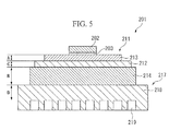
- the width of the metal layer 214 may be greater than the width of the circuit layer 213 or the insulating substrate 212.
- circuit layer and metal layer is composed of aluminum having a purity of 99.99% or more (4N aluminum) is described as an example, however, the present invention is not limited to this structure.
- the circuit layer and the metal layer may be composed of high purity aluminum (aluminum with a purity of greater than or equal to 99%, 2N aluminum) or an aluminum alloy.
- the present invention is not limited to this structure.
- the heatsink may be composed of pure aluminum.
- the heatsink having a flow passage of a cooling medium is described, however, the heatsink is not limited to a specific structure, for example, may be an air-cooled heatsink.
- the comparative examples 1 to 3 were compared with the examples 1 to 5.
Landscapes
- Chemical & Material Sciences (AREA)
- Engineering & Computer Science (AREA)
- Ceramic Engineering (AREA)
- Materials Engineering (AREA)
- Structural Engineering (AREA)
- Organic Chemistry (AREA)
- Cooling Or The Like Of Semiconductors Or Solid State Devices (AREA)
Abstract
Description
- The present invention relates to a power module substrate having a heatsink, which is employed to a semiconductor device controlling a large amount of electrical current and high voltage, a method for manufacturing the same, a power module having a heatsink, and a power module substrate.
- This application is based on and claims priority from Japanese Patent Application No.
2008-67344, filed on March 17, 2008 2008-234997, filed on September 12, 2008 - Conventionally, a power module substrate having a heatsink, which is employed to a semiconductor device controlling a large amount of electrical current and high voltage, is known.
- As this kind of the power module substrate, a structure in which a circuit layer composed of aluminum is formed on one face (a first face) of an insulating substrate, a metal layer composed of aluminum is formed on the other face (second face) of the insulating substrate, and a top panel portion of the heatsink is connected to a surface of the metal layer is widely proposed.
- The foregoing power module substrate is shown in, for example, Japanese Patent Publication No.
3171234 H10-065075 - The foregoing power module having a heatsink is manufactured so that the power module substrate is connected to the heatsink, after the power module substrate is formed by connecting the power module substrate, the insulating substrate, the circuit layer, and the metal layer together.
- In the power module substrate having a heatsink, electronic components such as a semiconductor chip are connected to the circuit layer by use of a solder.
- However, in the above-described power module substrate having a heatsink, if total thickness of the metal layer and the top panel portion of the heatsink which are positioned on the second face of the insulating substrate is small, the bending rigidity thereof is degraded, and warpage may occur thereon.
- In recent power modules having a heatsink, the size and thickness thereof have been reduced, but, the amount of heat generated in an electronic component has a tendency to increase.
- A heatsink in which the thickness of the top panel portion is small is employed in order to improve the cooling efficiency of the heatsink.
- Consequently, the total thickness of the metal layer and the top panel portion of the heatsink which are positioned on the second face of the insulating substrate become small, there is a problem in that the above-described warpage occurs.
- In addition, in the power module having a heatsink disclosed in Japanese Patent Publication No.
3171234 - Because of this, portions including a great amount of Si and having a high degree of hardness are formed at the joint interface between the aluminum foil and the metal layer and the joint interface between the aluminum foil and the heatsink.
- In the case where the portions having a high degree of hardness are formed at the metal layer and the heatsink which are positioned on the second face of the insulating substrate as mentioned above, the metal layer or the top panel portion of the heatsink is restrained at the portions having a high degree of hardness.
- For this reason, for example, when the power module substrate is connected to the heatsink, even if a pressure is applied in the stacking direction thereof, the metal layer is restrained by the portions having a high degree of hardness, it is not sufficiently deformed, and warpage cannot be suppressed.
- The present invention was conceived in view of the above-described circumstances and it is an object thereof to provide a power module substrate having a heatsink, a method for manufacturing the same, and a power module having a heatsink, in which it is possible to suppress the occurrence of warpage.
- In order to solve the foregoing problems and achieve the object, a power module substrate having a heatsink of a first aspect of the present invention, includes: a power module substrate having an insulating substrate having a first face and a second face, a circuit layer formed on the first face, and a metal layer formed on the second face; and a heatsink directly connected to the metal layer, cooling the power module substrate.
- Where the thickness of the circuit layer is represented as A, and the thickness of the metal layer is represented as B, the ratio B/A is in the range defined by 1.5 ≦ B/A ≦ 20.
- In the structure of the power module substrate having a heatsink, the ratio B/A is in the range defined by 1.5 ≦ B/A ≦ 20 as described above, namely, the thickness of the metal layer connected to the heatsink is greater than the thickness of the circuit layer.
- By employing this structure, even if a heatsink in which the thickness of the top panel portion is small is used, it is possible to relatively increase the total thickness of the metal layer and the top panel portion of the heatsink which are positioned on the second face of the insulating substrate, and it is possible to suppress the occurrence of warpage.
- In addition, since a thick metal layer is directly connected to the heatsink, when the power module substrate is connected to the heatsink, it is possible to sufficiently deform the metal layer by applying a pressure on the power module substrate and the heatsink in the stacking direction thereof, and it is possible to suppress warpage.
- Here, if the ratio B/A of the thickness B of the metal layer to the thickness A of the circuit layer is less than 1.5, it is not possible to sufficiently obtain the above-described effect.
- In contrast, if the ratio B/A of the thickness B of the metal layer to the thickness A of the circuit layer exceeds 20, the metal layer makes thermal resistance, and cooling by the heatsink does not become sufficient.
- Consequently, it is preferable that the ratio B/A of the thickness B of the metal layer to the thickness A of the circuit layer be in the range defined by 1.5 ≦ B/A ≦ 20.
- In addition, in the present invention, it is preferable that the metal layer be composed of aluminum having a purity of 99.99% or more, before being connected to the heatsink.
- By employing this structure, the deformation resistance of the metal layer is small, it is possible to sufficiently deform the metal layer by applying a pressure when the metal layer is connected to the heatsink, and it is possible to reliably suppress the occurrence of warpage.
- A method for manufacturing a power module substrate having a heatsink of a second aspect of the present invention, includes: preparing an insulating substrate having a first face and a second face, and a heatsink; connecting a circuit layer to the first face of the insulating substrate, and connecting a metal layer to the second face of the insulating substrate, thereby forming a power module substrate (first connecting step); and stacking the heatsink on the power module substrate in layers, and connecting the heatsink to the metal layer of the power module substrate by applying pressure of 0.15 to 3 MPa in a stacking direction (second connecting step).
- In the method for manufacturing the power module substrate having a heatsink having the structure, in the second connecting step in which the above-described power module substrate is connected to the heatsink, since the pressure of 0.15 to 3 MPa is applied in the stacking direction thereof, the metal layer is sufficiently deformed, therefore, it is possible to suppress the occurrence of warpage.
- A power module having a heatsink of a third aspect of the present invention includes: the above-described power module substrate having a heatsink; and an electronic component mounted on the circuit layer of the power module substrate having a heatsink.
- According to the power module having a heatsink, having this structure, warpage deformation is suppressed, it is possible to significantly improve the reliability thereof even if the usage environment thereof is strict, for example, a usage environment where stress is repeatedly generated.
- A power module substrate of a fourth aspect of the present invention includes: an insulating substrate having a first face and a second face; a circuit layer formed on the first face; and a metal layer formed on the second face.
- The ratio B/A of the thickness B of the metal layer to the thickness A of the circuit layer is in the range defined by 1.5 ≦ B/A ≦ 20.
- In the structure of the power module substrate, in the case where the heatsink is connected to the surface of the metal layer, even if a heatsink in which the thickness of the top panel portion is small is used, it is possible to relatively increase the total thickness of the metal layer and the top panel portion of the heatsink which are positioned on the second face of the insulating substrate, and it is thereby possible to suppress the occurrence of warpage.
- According to the present invention, it is possible to provide a power module substrate having a heatsink, a method for manufacturing the same, a power module having a heatsink, and a power module substrate, in which it is possible to suppress the occurrence of warpage.
-
-
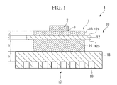
FIG. 1 is a schematic cross-sectional view showing a structure of a power module having a heatsink of embodiment of the present invention, in which a power module substrate having a heatsink is employed. -
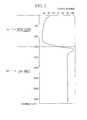
FIG. 2 is a view showing distribution of Vickers hardness of a metal layer and a top panel portion of the power module substrate having a heatsink of the embodiment of the present invention. -
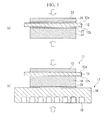
FIG. 3 is a schematic cross-sectional view illustrating a method for manufacturing a power module substrate having a heatsink of the embodiment of the present invention. -
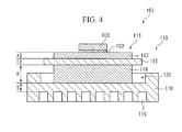
FIG. 4 is a schematic cross-sectional view showing the structure of a power module having a heatsink, in which a power module substrate having a heatsink of the other embodiment of the present invention is employed. -
FIG. 5 is a schematic cross-sectional view showing the structure of a power module having a heatsink, in which a power module substrate having a heatsink of the other embodiment of the present invention is employed. - Hereinafter, an embodiment of the present invention will be described with reference to attached drawings.
-
FIGS. 1 to 3(b) show a power module substrate having a heatsink and a power module having a heatsink of the embodiment of the present invention. - The power module 1 having a heatsink is provided with a
power module substrate 11 in which acircuit layer 13 is disposed, asemiconductor chip 2 to which the surface of thecircuit layer 13 is connected via a solder layer 3, and aheatsink 17. - Here, the solder layer 3 is made of, for example, Sn-Ag series, Sn-In series, or Sn-Ag-Cu series solder material.
- In addition, in the embodiment, Ni-plated layer (not shown) is provided between the
circuit layer 13 and the solder layer 3. - The
power module substrate 11 is provided with aninsulating substrate 12, acircuit layer 13 disposed on afirst face 12a of the insulating substrate 12 (upper face inFIG. 1 ), and ametal layer 14 disposed on asecond face 12b of the insulating substrate 12 (lower face inFIG. 1 ). - The
insulating substrate 12 is a substrate that prevents electrical connection between thecircuit layer 13 and themetal layer 14, and is composed of ceramics having a high degree of insulation such as AlN (aluminum nitride), Si3N4(silicon nitride), or Al2O3(alumina). - In the embodiment, the
insulating substrate 12 is composed of AlN (aluminum nitride). - In addition, in the embodiment, the thickness C of the
insulating substrate 12 is 0.635 mm, which is within the range of 0.2 mm ≦ C ≦ 1.5 mm. - The
circuit layer 13 is formed by brazing aconductive metal plate 23 to thefirst face 12a of theinsulating substrate 12. - In the embodiment, the
circuit layer 13 is formed by brazing themetal plate 23 composed of aluminum having a purity of 99.99% or more (a so-called 4N aluminum) to theinsulating substrate 12. - Here, in the embodiment, the brazing is performed by use of an Al-Si series brazing
filler metal foil 26, Si of the brazing filler metal is diffused into themetal plate 23, and distribution of Si-concentration thereby occurs in thecircuit layer 13. - The
circuit layer 14 is formed by brazing ametal plate 24 to thesecond face 12b of theinsulating substrate 12. - In the embodiment, the
metal layer 24 is formed by brazing themetal plate 24 composed of aluminum having a purity of 99.99% or more (a so-called 4N aluminum) to theinsulating substrate 12, similarly to thecircuit layer 13. - In the embodiment, the brazing is performed by use of an Al-Si series brazing
filler metal foil 27, Si of the brazing filler metal is diffused into themetal plate 24, and distribution of Si-concentration thereby occurs in themetal layer 14. - Here, in the embodiment, the thickness A of the
circuit layer 13 is 0.6 mm, which is within the range of 0.25 mm ≦ A ≦ 0.9 mm. - In addition, in the embodiment, the thickness B of the
metal layer 14 is 1.3 mm, which is within the range of 0.4 mm ≦ B ≦ 5 mm. - Consequently, in the embodiment, the ratio B/A of the thickness B of the
metal layer 14 to the thickness A of thecircuit layer 13 is 1.3/0.6, that is, 2.167, which is within the range of 1.5 ≦ B/A ≦ 20. - The
heatsink 17 is a component cooling the above-describedpower module substrate 11, and is provided with atop panel portion 18 connected to thepower module substrate 11 and aflow passage 19 in which a cooling medium (for example, cooling water) flows. - At least the
top panel portion 18 is desirably composed of a material having excellent thermal conductivity in theheatsink 17, and is composed of aluminum material of A6063 in the embodiment. - In addition, in the embodiment, the thickness D of the
top panel portion 18 is 1.7 mm, which is within the range of 1 mm ≦ D ≦ 10 mm. - Consequently, the
metal layer 14 of thepower module substrate 11 is directly connected to thetop panel portion 18 of theheatsink 17 by brazing. - In the embodiment, the brazing is performed by use of an Al-Si series brazing
filler metal foil 28, Si of the brazing filler metal is diffused into themetal plate 24, and distribution of Si-concentration thereby occurs in themetal layer 14. - As described above, the
metal layer 14 is brazed with the insulatingsubstrate 12 by use of the brazingfiller metal foil 27, and is brazed with thetop panel portion 18 of theheatsink 17 by use of the brazingfiller metal foil 28. - Because of this, as shown in
FIG. 2 , due to the distribution of Si-concentration, Vickers hardness varies in themetal layer 14 along the thickness direction thereof. - The foregoing
power module substrate 10 having a heatsink is manufactured as described below. - As shown in
FIG. 3(a) , firstly, an insulatingsubstrate 12 composed of AlN is prepared. - Next, a
circuit layer 13 that becomes a metal plate 23 (4N aluminum) is stacked on afirst face 12a of the insulatingsubstrate 12 in layers with a brazingfiller metal foil 26 interposed therebetween. - The thickness of the brazing
filler metal foil 26 is 0.02 mm. - In addition, a
metal layer 14 that becomes a metal plate 24 (4N aluminum) is stacked on asecond face 12b of the insulatingsubstrate 12 in layers with brazingfiller metal foil 27 interposed therebetween. - The thickness of the brazing
filler metal foil 27 is the same as that of the brazingfiller metal foil 26. - Subsequently, the layered body was formed in the above-described manner, the layered body is set inside of a vacuum furnace in a state where a pressure is applied to the layered body in the stacking direction thereof, and brazing is performed.
- Therefore, a
power module substrate 11 that is constituted of the insulatingsubstrate 12, thecircuit layer 13, and themetal layer 14 is formed (first connecting step S1). - Next, as shown in
FIG. 3(b) , thetop panel portion 18 of theheatsink 17 is stacked on the surface of themetal layer 14 of thepower module substrate 11 in layers with a brazingfiller metal foil 28 interposed therebetween. - The thickness of the brazing
filler metal foil 28 is 0.05 mm. - A pressure is applied in the stacking direction in a state of being stacked as stated above and brazing is performed in the vacuum furnace, the
power module substrate 10 having a heatsink of the embodiment is manufactured (second connecting step S2). - Here, in the second connecting step S2, the pressure of 0.15 to 3 MPa is applied to the
power module substrate 11 and theheatsink 17 in the stacking direction. - In the
power module substrate 10 having a heatsink and the power module 1 having a heatsink of the embodiment, which have the foregoing structure, the thickness of themetal layer 14 connected to thetop panel portion 18 of theheatsink 17 is greater than the thickness of thecircuit layer 13. - Consequently, even if the
heatsink 17 in which the thickness of thetop panel portion 18 is small is used, the total thickness of themetal layer 14 and thetop panel portion 18 of theheatsink 17 which are positioned on thesecond face 12b of the insulatingsubstrate 12 can be ensured, and it is possible to suppress the occurrence of warpage. - In addition, since the
heatsink 17 in which thetop panel portion 18 is thin is used, it is possible to improve the cooling efficiency, and it is possible to apply it to the power module in which electronic components having a high level of heat generation are packaged. - In addition, a relatively
thick metal layer 14 is directly connected to thetop panel portion 18 of theheatsink 17 by brazing and using the brazingfiller metal foil 28. - Because of this, in the second connecting step S2 in which the
power module substrate 11 is connected to thetop panel portion 18 of theheatsink 17, it is possible to sufficiently deform themetal layer 14 when the pressure is applied to thepower module substrate 11 and theheatsink 17 in the stacking direction thereof, and it is possible to reliably suppress warpage. - Furthermore, in the embodiment, the ratio B/A of the thickness B of the
metal layer 14 to the thickness A of thecircuit layer 13 is 1.3/0.6, that is, 2.167, which is within the range of 1.5 ≦ B/A ≦ 20. - Consequently, the thickness of the
metal layer 14 is ensured, and it is possible to reliably obtain the effect that the above-described warpage is suppressed. - In addition, the
metal layer 14 does not become a high degree of thermal resistance, it is possible to sufficiently cool the power module using theheatsink 17. - In addition, it is preferable that the ratio B/A of the thickness B of the
metal layer 14 to the thickness A of thecircuit layer 13 be in the range defined by 2.157 ≦ B/A ≦ 5.625. - In addition, the
metal layer 14 is composed of aluminum having a purity of 99.99% or more, that is, a so-called 4N aluminum, before being connected. - For this reason, the deformation resistance of the
metal layer 14 is small, it is possible to sufficiently deform themetal layer 14 when the pressure is applied in the stacking direction in the second connecting step S2 in which themetal layer 14 is connected to thetop panel portion 18 of theheatsink 17, and it is possible to reliably suppress the occurrence of warpage. - In addition, in the second connecting step S2 in which the
metal layer 14 is connected to thetop panel portion 18 of theheatsink 17, since thepower module substrate 11 and theheatsink 17 is pressed by applying the pressure of 0.15 to 3 MPa in the stacking direction, themetal layer 14 is reliably deformed, and it is possible to suppress warpage. - In addition, in the power module 1 having a heatsink of the embodiment, the
semiconductor chip 2 is connected to thecircuit layer 13 of thepower module substrate 10 having a heatsink by use of the solder. - Therefore, since warpage deformation does not occur, it is possible to significantly improve the reliability, even if the usage environment is strict, for example, the usage environment where stress is repeatedly generated.
- The embodiment of the present invention is described above, however, the present invention is not limited to the above embodiment, and various modifications may be made without departing from the scope of the invention.
- For example, in the above-described embodiment, the case where AlN (aluminum nitride) is adopted as a material of the insulating
substrate 12 is described, however, materials having an insulation property such as Si3N4 or Al2O3 may be adopted. - In addition, the structure in which the
power module substrate 11 is connected to thetop panel portion 18 formed in a tabular shape is described, however, the present invention is not limited to this structure. - For example, as shown in
FIG. 4 , a recessedportion 120 may be formed on thetop panel portion 118, and thepower module substrate 111 may be contained in the recessedportion 120. - In this case, the thickness D of the
top panel portion 118 is the thickness of the bottom face of the recessedportion 120. - Moreover, the structure in which the width of the
metal layer 14 is the same as that of thecircuit layer 13 and is narrower than that of the insulatingsubstrate 12 is described in the above-described embodiment, however, the present invention is not limited to this structure. - For example, as shown in
FIG. 5 , the width of themetal layer 214 may be greater than the width of thecircuit layer 213 or the insulatingsubstrate 212. - In this case, alignment with a high level of precision is not necessary when the
metal layer 214 is connected to the insulatingsubstrate 212, it is possible to manufacture the power module substrate having a heatsink 210 in a relatively simple manner. - In addition, the structure in which the circuit layer and metal layer is composed of aluminum having a purity of 99.99% or more (4N aluminum) is described as an example, however, the present invention is not limited to this structure.
- The circuit layer and the metal layer may be composed of high purity aluminum (aluminum with a purity of greater than or equal to 99%, 2N aluminum) or an aluminum alloy.
- However, it is preferable that aluminum having a purity of 99.99% or more be used, because the deformation resistance of the metal layer become small and it is possible to reliably obtain the effect that warpage is suppressed.
- Additionally, the structure in which the heatsink is composed of aluminum matetial of A6063 is described as an example, the present invention is not limited to this structure.
- The heatsink may be composed of pure aluminum.
- Furthermore, the heatsink, having a flow passage of a cooling medium is described, however, the heatsink is not limited to a specific structure, for example, may be an air-cooled heatsink.
- A comparison experiment will be described in order to evaluate effectivity of the present invention.
- In the comparative examples 1 to 3 and the examples 1 to 5, common power module substrates having a heatsink were prepared, including an insulating substrate composed of AlN having a thickness of 0.635 mm, a circuit layer and a metal layer composed of 4N aluminum, and a heatsink provided with a top panel portion composed of aluminum matetial of A6063 having a thickness of 1.7 mm. In addition, in the power module substrate having a heatsink, the metal layer was directly connected to the top panel portion of the heatsink by brazing.
- Consequently, each of the thickness of the circuit layer and the thickness of the metal layer of the power module substrate having a heatsink was changed, and the power module substrates having a heatsink of the comparative examples 1 to 3 and the examples 1 to 5 were thereby manufactured.
- In the examples, a state where warpage occurs in the manufactured power module substrate having a heatsink, and the thermal resistance between the heatsink, and the insulating substrate are evaluated.
- The comparative examples 1 to 3 were compared with the examples 1 to 5.
- The evaluation result is shown in Table 1.
TABLE 1 COMPARATIVE EXAMPLE 1 COMPARATIVE EXAMPLE 2 EXAMPLE 1 EXAMPLE 2 EXAMPLE 3 EXAMPLE 4 EXAMPLE 5 COMPARATIVE EXAMPLE 3 THICKNESS A OF CIRCUIT LAYER 0.6mm 0.6mm 0.6mm 0.6mm 0.4mm 0.4mm 0.25mm 0.4mm THICKNESS B OF METAL LAYER 0.6mm 0.75mm 0.9mm 1.3mm 2.25mm 5mm 5mm 10mm B/A 1 1.25 1.5 2.167 5.625 12.5 20 25 WARPAGE DEFORMATION × △ ○ ○ ○ ○ ○ ○ THERMAL RESISTANCE ○ ○ ○ ○ ○ ○ ○ × - In the comparative examples 1 and 2, since the metal layer is relatively thin, the thermal resistance thereof is small, however, warpage deformation is confirmed.
- In contrast, as shown in the comparative example 3, in the case where the metal layer is significantly thick compared with the circuit layer, thermal resistance is high, and it is confirmed that cooling by the heatsink does not become sufficient.
- In contrast, in the examples 1 to 5, it was found that warpage deformation was suppressed, and the thermal resistance was suppressed so as to be small.
- As a result of comparison experiment, according to the present invention, it is confirmed that it is possible to provide the power module substrate having a heatsink in which warpage deformation does not occur and which is capable of effectively cooling electronic components or the like by the heatsink.
Claims (6)
- A power module substrate having a heatsink, comprising:a power module substrate having an insulating substrate having a first face and a second face, a circuit layer formed on the first face, and a metal layer formed on the second face; anda heatsink directly connected to the metal layer, cooling the power module substrate, whereina ratio B/A is in the range defined by 1.5 ≦ B/A ≦ 20, where a thickness of the circuit layer is represented as A, and a thickness of the metal layer is represented as B.
- The power module substrate having a heatsink according to claim 1, wherein
the metal layer is composed of aluminum having a purity of 99.99% or more, before being connected to the heatsink. - A method for manufacturing a power module substrate having a heatsink, comprising:preparing an insulating substrate having a first face and a second face, and a heatsink;connecting a circuit layer to the first face of the insulating substrate, and connecting a metal layer to the second face of the insulating substrate, thereby forming a power module substrate; andstacking the heatsink on the power module substrate in layers, and connecting the heatsink to the metal layer of the power module substrate by applying pressure of 0.15 to 3 MPa in a stacking direction.
- The method for manufacturing the power module substrate having a heatsink according to claim 3, wherein
the metal layer is composed of aluminum having a purity of 99.99% or more, before being connected to the heatsink. - A power module having a heatsink, comprising:the power module substrate having a heatsink according to claim 1 or claim 2; andan electronic component mounted on the circuit layer of the power module substrate having a heatsink.
- A power module substrate comprising:an insulating substrate having a first face and a second face;a circuit layer formed on the first face; anda metal layer formed on the second face, whereina ratio B/A is in the range defined by 1.5 ≦ B/A ≦ 20, where a thickness of the circuit layer is represented as A, and a thickness of the metal layer is represented as B.
Applications Claiming Priority (3)
| Application Number | Priority Date | Filing Date | Title |
|---|---|---|---|
| JP2008067344 | 2008-03-17 | ||
| JP2008234997 | 2008-09-12 | ||
| PCT/JP2009/054654 WO2009116439A1 (en) | 2008-03-17 | 2009-03-11 | Substrate for power module with heat sink and method for producing the same, power module with heat sink, and substrate for power module |
Publications (3)
| Publication Number | Publication Date |
|---|---|
| EP2259308A1 true EP2259308A1 (en) | 2010-12-08 |
| EP2259308A4 EP2259308A4 (en) | 2014-11-05 |
| EP2259308B1 EP2259308B1 (en) | 2022-06-15 |
Family
ID=41090843
Family Applications (1)
| Application Number | Title | Priority Date | Filing Date |
|---|---|---|---|
| EP09721361.5A Active EP2259308B1 (en) | 2008-03-17 | 2009-03-11 | Substrate for power module with heat sink and method for producing the same, power module with heat sink, and substrate for power module |
Country Status (6)
| Country | Link |
|---|---|
| US (1) | US8637777B2 (en) |
| EP (1) | EP2259308B1 (en) |
| JP (4) | JP4524716B2 (en) |
| KR (1) | KR101610973B1 (en) |
| CN (1) | CN101971329B (en) |
| WO (1) | WO2009116439A1 (en) |
Cited By (4)
| Publication number | Priority date | Publication date | Assignee | Title |
|---|---|---|---|---|
| EP2525637A4 (en) * | 2010-01-12 | 2015-06-24 | Nippon Light Metal Co | LIQUID COOLED INTEGRATED SUBSTRATE AND METHOD FOR MANUFACTURING A LIQUID COOLED INTEGRATED SUBSTRATE |
| EP2980844A4 (en) * | 2013-03-29 | 2016-11-02 | Mitsubishi Materials Corp | SUBSTRATE FOR POWER MODULES, SUBSTRATE HAVING THERMAL DISSIPATOR FOR POWER MODULES, AND POWER MODULE |
| EP3093856A4 (en) * | 2014-01-08 | 2017-09-13 | Mitsubishi Materials Corporation | Resistor and production method for resistor |
| DE102022204169A1 (en) | 2022-04-28 | 2023-11-02 | Robert Bosch Gesellschaft mit beschränkter Haftung | Electronic assembly |
Families Citing this family (43)
| Publication number | Priority date | Publication date | Assignee | Title |
|---|---|---|---|---|
| JP5640570B2 (en) * | 2009-09-09 | 2014-12-17 | 三菱マテリアル株式会社 | Power module substrate manufacturing method |
| JP5640569B2 (en) * | 2009-09-09 | 2014-12-17 | 三菱マテリアル株式会社 | Power module substrate manufacturing method |
| JP2011119653A (en) * | 2009-09-09 | 2011-06-16 | Mitsubishi Materials Corp | Method for producing substrate for power module with heat sink, substrate for power module with heat sink, and power module |
| JP5479181B2 (en) * | 2010-03-30 | 2014-04-23 | 株式会社豊田中央研究所 | Insulating substrate and module having the insulating substrate |
| JP5614127B2 (en) * | 2010-06-28 | 2014-10-29 | 三菱マテリアル株式会社 | Power module substrate and manufacturing method thereof |
| JP2012049437A (en) * | 2010-08-30 | 2012-03-08 | Mitsubishi Materials Corp | Substrate for power module and method of manufacturing the same |
| JP5577980B2 (en) * | 2010-09-16 | 2014-08-27 | 三菱マテリアル株式会社 | Power module substrate with heat sink, power module, and method for manufacturing power module substrate with heat sink |
| JP5392272B2 (en) * | 2011-01-13 | 2014-01-22 | 株式会社豊田自動織機 | Double-sided substrate, semiconductor device, and method for manufacturing semiconductor device |
| JP6122573B2 (en) * | 2011-01-14 | 2017-04-26 | 日本軽金属株式会社 | Method for manufacturing liquid-cooled integrated substrate |
| JP5678684B2 (en) * | 2011-01-24 | 2015-03-04 | 三菱マテリアル株式会社 | Power module substrate manufacturing method |
| JP5786569B2 (en) * | 2011-09-05 | 2015-09-30 | 三菱マテリアル株式会社 | Power module substrate manufacturing method |
| US9810416B2 (en) * | 2011-10-26 | 2017-11-07 | Hangzhou Hpwinner Opto Corporation | Method for manufacturing a lamp-housing-type heat-sink, lamp-housing-type heat-sink, and LED lighting device |
| CN103988297B (en) * | 2011-12-12 | 2018-11-23 | 三菱综合材料株式会社 | Power module and its manufacturing method |
| KR101367211B1 (en) * | 2012-02-13 | 2014-02-26 | 광전자 주식회사 | Aluminum Base Plate for Power Module |
| JP6127540B2 (en) * | 2012-03-30 | 2017-05-17 | 三菱マテリアル株式会社 | Power module substrate manufacturing method |
| JP2014112732A (en) * | 2012-03-30 | 2014-06-19 | Mitsubishi Materials Corp | Substrate for power module with heat sink and power module |
| JP2013229579A (en) | 2012-03-30 | 2013-11-07 | Mitsubishi Materials Corp | Substrate for power module, substrate for power module having heat sink, and power module |
| JP5548722B2 (en) | 2012-03-30 | 2014-07-16 | 三菱マテリアル株式会社 | Power module substrate with heat sink, and method for manufacturing power module substrate with heat sink |
| JP5987418B2 (en) * | 2012-03-30 | 2016-09-07 | 三菱マテリアル株式会社 | Manufacturing method of power module substrate with heat sink |
| KR101540146B1 (en) | 2012-06-22 | 2015-07-28 | 삼성전기주식회사 | Heat dissipation system for power module |
| US8941208B2 (en) * | 2012-07-30 | 2015-01-27 | General Electric Company | Reliable surface mount integrated power module |
| JP6201297B2 (en) * | 2012-11-08 | 2017-09-27 | 三菱マテリアル株式会社 | Power module substrate with copper plate and method for manufacturing power module substrate with copper plate |
| JP6056432B2 (en) * | 2012-12-06 | 2017-01-11 | 三菱マテリアル株式会社 | Power module substrate, power module substrate with heat sink, power module, power module substrate manufacturing method |
| JP5971171B2 (en) * | 2013-03-28 | 2016-08-17 | トヨタ自動車株式会社 | Insulating substrate, manufacturing method thereof, and semiconductor device |
| CN105189409B (en) * | 2013-03-29 | 2018-11-09 | 三菱综合材料株式会社 | Manufacturing apparatus and manufacturing method of metal-ceramic plate laminate, manufacturing apparatus and manufacturing method of substrate for power module |
| JP6116404B2 (en) * | 2013-07-01 | 2017-04-19 | 昭和電工株式会社 | Heat dissipation device |
| JP6139329B2 (en) * | 2013-08-16 | 2017-05-31 | 日本碍子株式会社 | Ceramic circuit board and electronic device |
| JP5949817B2 (en) * | 2014-03-20 | 2016-07-13 | 三菱マテリアル株式会社 | Power module substrate manufacturing method |
| JP6287428B2 (en) * | 2014-03-25 | 2018-03-07 | 三菱マテリアル株式会社 | Manufacturing method of power module substrate with heat sink |
| JP6384112B2 (en) * | 2014-04-25 | 2018-09-05 | 三菱マテリアル株式会社 | Power module substrate and power module substrate with heat sink |
| EP3166140B1 (en) * | 2014-07-04 | 2020-06-03 | Mitsubishi Materials Corporation | Substrate unit for power modules, and power module |
| US10109555B2 (en) | 2015-02-02 | 2018-10-23 | Kabushiki Kaisha Toshiba | Silicon nitride circuit board and electronic component module using the same |
| JP6638282B2 (en) * | 2015-09-25 | 2020-01-29 | 三菱マテリアル株式会社 | Light emitting module with cooler and method of manufacturing light emitting module with cooler |
| JP2017224748A (en) * | 2016-06-16 | 2017-12-21 | 株式会社Uacj | Heat sink with circuit board and manufacturing method thereof |
| CN107683016A (en) * | 2017-11-21 | 2018-02-09 | 生益电子股份有限公司 | A fast heat dissipation PCB |
| CN111466140B (en) | 2017-12-25 | 2021-12-03 | 华为技术有限公司 | Parameter adjusting method and related equipment |
| JP7119689B2 (en) * | 2018-07-19 | 2022-08-17 | 三菱マテリアル株式会社 | Manufacturing method of insulated circuit board with heat sink and insulated circuit board with heat sink |
| JP7363613B2 (en) * | 2020-03-13 | 2023-10-18 | 三菱マテリアル株式会社 | Insulated circuit board with integrated heat sink |
| JP7717699B6 (en) * | 2020-07-27 | 2025-08-27 | 株式会社東芝 | Joint, circuit board, semiconductor device, and method for manufacturing joint |
| KR102720892B1 (en) * | 2021-07-27 | 2024-10-23 | 주식회사 아모센스 | Ceramic substrate with heat sink and manufacturing method thereof |
| KR102923495B1 (en) * | 2022-09-23 | 2026-02-05 | 주식회사 아모그린텍 | Power module substrate with heat sink and manufacturing method thereof |
| EP4539117A1 (en) * | 2023-05-22 | 2025-04-16 | LX Semicon Co., Ltd. | A heat dissipation substrate for a power semiconductor module, a power semiconductor module including the heat dissipation substrate, and a power converter including the power semiconductor module |
| EP4539116A1 (en) * | 2023-05-22 | 2025-04-16 | LX Semicon Co., Ltd. | A heat dissipation substrate for a power semiconductor module, a power semiconductor module including the heat dissipation substrate, and a power converter including the power semiconductor module |
Family Cites Families (17)
| Publication number | Priority date | Publication date | Assignee | Title |
|---|---|---|---|---|
| JPH0723964Y2 (en) * | 1988-11-11 | 1995-05-31 | 三菱マテリアル株式会社 | Lightweight substrate for semiconductor device |
| JP3171234B2 (en) | 1997-03-26 | 2001-05-28 | 三菱マテリアル株式会社 | Ceramic circuit board with heat sink |
| JP3180677B2 (en) | 1996-08-22 | 2001-06-25 | 三菱マテリアル株式会社 | Ceramic circuit board with heat sink |
| JP4556307B2 (en) * | 2000-08-11 | 2010-10-06 | 三菱マテリアル株式会社 | Power module and method for manufacturing power module cushioning material |
| US6707671B2 (en) * | 2001-05-31 | 2004-03-16 | Matsushita Electric Industrial Co., Ltd. | Power module and method of manufacturing the same |
| JP4077181B2 (en) * | 2001-09-27 | 2008-04-16 | 本田技研工業株式会社 | Metal or ceramic bonding material and metal or ceramic bonding method |
| JP4387658B2 (en) * | 2002-10-30 | 2009-12-16 | 三菱マテリアル株式会社 | Ceramic circuit board with heat sink and manufacturing method thereof |
| JP3938079B2 (en) * | 2003-03-20 | 2007-06-27 | 三菱マテリアル株式会社 | Power module substrate manufacturing method |
| JP4438526B2 (en) * | 2004-06-16 | 2010-03-24 | 株式会社安川電機 | Power component cooling system |
| KR100765604B1 (en) * | 2004-11-26 | 2007-10-09 | 산요덴키가부시키가이샤 | Circuit device and manufacturing method thereof |
| JP4207896B2 (en) * | 2005-01-19 | 2009-01-14 | 富士電機デバイステクノロジー株式会社 | Semiconductor device |
| JP4037425B2 (en) | 2005-07-04 | 2008-01-23 | 電気化学工業株式会社 | Ceramic circuit board and power control component using the same. |
| JP5061442B2 (en) * | 2005-09-15 | 2012-10-31 | 三菱マテリアル株式会社 | Insulated circuit board and insulated circuit board with cooling sink |
| WO2007105361A1 (en) * | 2006-03-08 | 2007-09-20 | Kabushiki Kaisha Toshiba | Electronic component module |
| JP4786407B2 (en) * | 2006-05-18 | 2011-10-05 | 三菱マテリアル株式会社 | Power module |
| JP2008004871A (en) * | 2006-06-26 | 2008-01-10 | Mitsubishi Materials Corp | Power module substrate, power module substrate manufacturing method, and power module |
| JP5392272B2 (en) | 2011-01-13 | 2014-01-22 | 株式会社豊田自動織機 | Double-sided substrate, semiconductor device, and method for manufacturing semiconductor device |
-
2009
- 2009-03-11 KR KR1020107017399A patent/KR101610973B1/en not_active Expired - Fee Related
- 2009-03-11 WO PCT/JP2009/054654 patent/WO2009116439A1/en not_active Ceased
- 2009-03-11 CN CN2009801091880A patent/CN101971329B/en active Active
- 2009-03-11 US US12/922,732 patent/US8637777B2/en not_active Expired - Fee Related
- 2009-03-11 EP EP09721361.5A patent/EP2259308B1/en active Active
- 2009-03-16 JP JP2009063210A patent/JP4524716B2/en not_active Expired - Fee Related
-
2010
- 2010-03-10 JP JP2010053620A patent/JP5434701B2/en active Active
-
2013
- 2013-01-18 JP JP2013007864A patent/JP5440721B2/en active Active
- 2013-06-20 JP JP2013129704A patent/JP5613914B2/en active Active
Cited By (7)
| Publication number | Priority date | Publication date | Assignee | Title |
|---|---|---|---|---|
| EP2525637A4 (en) * | 2010-01-12 | 2015-06-24 | Nippon Light Metal Co | LIQUID COOLED INTEGRATED SUBSTRATE AND METHOD FOR MANUFACTURING A LIQUID COOLED INTEGRATED SUBSTRATE |
| US9320129B2 (en) | 2010-01-12 | 2016-04-19 | Dowa Metaltech Co., Ltd. | Liquid-cooled integrated substrate and manufacturing method of liquid-cooled integrated substrate |
| EP2980844A4 (en) * | 2013-03-29 | 2016-11-02 | Mitsubishi Materials Corp | SUBSTRATE FOR POWER MODULES, SUBSTRATE HAVING THERMAL DISSIPATOR FOR POWER MODULES, AND POWER MODULE |
| US9807865B2 (en) | 2013-03-29 | 2017-10-31 | Mitsubishi Materials Corporation | Substrate for power modules, substrate with heat sink for power modules, and power module |
| EP3093856A4 (en) * | 2014-01-08 | 2017-09-13 | Mitsubishi Materials Corporation | Resistor and production method for resistor |
| US10037837B2 (en) | 2014-01-08 | 2018-07-31 | Mitsubishi Materials Corporation | Resistor and method for manufacturing resistor |
| DE102022204169A1 (en) | 2022-04-28 | 2023-11-02 | Robert Bosch Gesellschaft mit beschränkter Haftung | Electronic assembly |
Also Published As
| Publication number | Publication date |
|---|---|
| EP2259308B1 (en) | 2022-06-15 |
| CN101971329A (en) | 2011-02-09 |
| JP5440721B2 (en) | 2014-03-12 |
| JP2013065918A (en) | 2013-04-11 |
| JP5434701B2 (en) | 2014-03-05 |
| JP5613914B2 (en) | 2014-10-29 |
| JP2010171437A (en) | 2010-08-05 |
| KR20100138875A (en) | 2010-12-31 |
| CN101971329B (en) | 2012-11-21 |
| KR101610973B1 (en) | 2016-04-08 |
| JP2013179374A (en) | 2013-09-09 |
| US20110017496A1 (en) | 2011-01-27 |
| JP4524716B2 (en) | 2010-08-18 |
| JP2010093225A (en) | 2010-04-22 |
| US8637777B2 (en) | 2014-01-28 |
| WO2009116439A1 (en) | 2009-09-24 |
| EP2259308A4 (en) | 2014-11-05 |
Similar Documents
| Publication | Publication Date | Title |
|---|---|---|
| EP2259308B1 (en) | Substrate for power module with heat sink and method for producing the same, power module with heat sink, and substrate for power module | |
| EP3057125B1 (en) | Substrate for heat sink-equipped power module, and production method for same | |
| EP2980844B1 (en) | Substrate for power modules, substrate with heat sink for power modules, and power module | |
| US9269644B2 (en) | Method for producing semiconductor device | |
| EP3136431B1 (en) | Substrate for power modules, substrate with heat sink for power modules and power module with heat sink | |
| EP1667508B1 (en) | Ceramic circuit board, method for making the same, and power module | |
| EP3358615B1 (en) | Silicon nitride circuit board and semiconductor module using same | |
| JP2013065918A5 (en) | ||
| JP6907546B2 (en) | Power module | |
| JP4683043B2 (en) | Manufacturing method of semiconductor device | |
| KR20200135378A (en) | Electronic component mounting module | |
| JP5002614B2 (en) | Manufacturing method of ceramic circuit board | |
| JP5772088B2 (en) | Power module substrate manufacturing method and power module substrate | |
| KR102564818B1 (en) | Power module and manufacturing method thereof | |
| CN117099200A (en) | Methods of manufacturing power modules | |
| JP2004296493A (en) | Heat radiator, power module, method of manufacturing heat radiator, and method of manufacturing power module | |
| EP4444674B1 (en) | Integrated substrates and related methods | |
| HK1151627A (en) | Substrate for power module with heat sink and method for producing the same, power module with heat sink, and substrate for power module | |
| JP2003124584A (en) | Ceramic circuit board | |
| EP4639619A1 (en) | A design for enhancing the long term reliability of a large joining area in a power semiconductor module |
Legal Events
| Date | Code | Title | Description |
|---|---|---|---|
| PUAI | Public reference made under article 153(3) epc to a published international application that has entered the european phase |
Free format text: ORIGINAL CODE: 0009012 |
|
| 17P | Request for examination filed |
Effective date: 20100922 |
|
| AK | Designated contracting states |
Kind code of ref document: A1 Designated state(s): AT BE BG CH CY CZ DE DK EE ES FI FR GB GR HR HU IE IS IT LI LT LU LV MC MK MT NL NO PL PT RO SE SI SK TR |
|
| AX | Request for extension of the european patent |
Extension state: AL BA RS |
|
| DAX | Request for extension of the european patent (deleted) | ||
| A4 | Supplementary search report drawn up and despatched |
Effective date: 20141008 |
|
| RIC1 | Information provided on ipc code assigned before grant |
Ipc: H01L 23/12 20060101AFI20141001BHEP Ipc: H01L 23/373 20060101ALI20141001BHEP |
|
| STAA | Information on the status of an ep patent application or granted ep patent |
Free format text: STATUS: EXAMINATION IS IN PROGRESS |
|
| 17Q | First examination report despatched |
Effective date: 20180111 |
|
| RAP1 | Party data changed (applicant data changed or rights of an application transferred) |
Owner name: MITSUBISHI MATERIALS CORPORATION |
|
| GRAP | Despatch of communication of intention to grant a patent |
Free format text: ORIGINAL CODE: EPIDOSNIGR1 |
|
| STAA | Information on the status of an ep patent application or granted ep patent |
Free format text: STATUS: GRANT OF PATENT IS INTENDED |
|
| INTG | Intention to grant announced |
Effective date: 20220310 |
|
| RIN1 | Information on inventor provided before grant (corrected) |
Inventor name: KUROMITSU, YOSHIROU Inventor name: ISHIZUKA, HIROYA Inventor name: TONOMURA, HIROSHI Inventor name: KITAHARA, TAKESHI Inventor name: HAYASHI, HIROMASA |
|
| GRAS | Grant fee paid |
Free format text: ORIGINAL CODE: EPIDOSNIGR3 |
|
| GRAA | (expected) grant |
Free format text: ORIGINAL CODE: 0009210 |
|
| STAA | Information on the status of an ep patent application or granted ep patent |
Free format text: STATUS: THE PATENT HAS BEEN GRANTED |
|
| AK | Designated contracting states |
Kind code of ref document: B1 Designated state(s): AT BE BG CH CY CZ DE DK EE ES FI FR GB GR HR HU IE IS IT LI LT LU LV MC MK MT NL NO PL PT RO SE SI SK TR |
|
| REG | Reference to a national code |
Ref country code: CH Ref legal event code: EP Ref country code: GB Ref legal event code: FG4D |
|
| REG | Reference to a national code |
Ref country code: IE Ref legal event code: FG4D |
|
| REG | Reference to a national code |
Ref country code: DE Ref legal event code: R096 Ref document number: 602009064479 Country of ref document: DE |
|
| REG | Reference to a national code |
Ref country code: AT Ref legal event code: REF Ref document number: 1498893 Country of ref document: AT Kind code of ref document: T Effective date: 20220715 |
|
| REG | Reference to a national code |
Ref country code: LT Ref legal event code: MG9D |
|
| REG | Reference to a national code |
Ref country code: NL Ref legal event code: MP Effective date: 20220615 |
|
| PG25 | Lapsed in a contracting state [announced via postgrant information from national office to epo] |
Ref country code: SE Free format text: LAPSE BECAUSE OF FAILURE TO SUBMIT A TRANSLATION OF THE DESCRIPTION OR TO PAY THE FEE WITHIN THE PRESCRIBED TIME-LIMIT Effective date: 20220615 Ref country code: NO Free format text: LAPSE BECAUSE OF FAILURE TO SUBMIT A TRANSLATION OF THE DESCRIPTION OR TO PAY THE FEE WITHIN THE PRESCRIBED TIME-LIMIT Effective date: 20220915 Ref country code: LT Free format text: LAPSE BECAUSE OF FAILURE TO SUBMIT A TRANSLATION OF THE DESCRIPTION OR TO PAY THE FEE WITHIN THE PRESCRIBED TIME-LIMIT Effective date: 20220615 Ref country code: HR Free format text: LAPSE BECAUSE OF FAILURE TO SUBMIT A TRANSLATION OF THE DESCRIPTION OR TO PAY THE FEE WITHIN THE PRESCRIBED TIME-LIMIT Effective date: 20220615 Ref country code: GR Free format text: LAPSE BECAUSE OF FAILURE TO SUBMIT A TRANSLATION OF THE DESCRIPTION OR TO PAY THE FEE WITHIN THE PRESCRIBED TIME-LIMIT Effective date: 20220916 Ref country code: FI Free format text: LAPSE BECAUSE OF FAILURE TO SUBMIT A TRANSLATION OF THE DESCRIPTION OR TO PAY THE FEE WITHIN THE PRESCRIBED TIME-LIMIT Effective date: 20220615 Ref country code: BG Free format text: LAPSE BECAUSE OF FAILURE TO SUBMIT A TRANSLATION OF THE DESCRIPTION OR TO PAY THE FEE WITHIN THE PRESCRIBED TIME-LIMIT Effective date: 20220915 |
|
| REG | Reference to a national code |
Ref country code: AT Ref legal event code: MK05 Ref document number: 1498893 Country of ref document: AT Kind code of ref document: T Effective date: 20220615 |
|
| PG25 | Lapsed in a contracting state [announced via postgrant information from national office to epo] |
Ref country code: LV Free format text: LAPSE BECAUSE OF FAILURE TO SUBMIT A TRANSLATION OF THE DESCRIPTION OR TO PAY THE FEE WITHIN THE PRESCRIBED TIME-LIMIT Effective date: 20220615 |
|
| PG25 | Lapsed in a contracting state [announced via postgrant information from national office to epo] |
Ref country code: NL Free format text: LAPSE BECAUSE OF FAILURE TO SUBMIT A TRANSLATION OF THE DESCRIPTION OR TO PAY THE FEE WITHIN THE PRESCRIBED TIME-LIMIT Effective date: 20220615 |
|
| PG25 | Lapsed in a contracting state [announced via postgrant information from national office to epo] |
Ref country code: SK Free format text: LAPSE BECAUSE OF FAILURE TO SUBMIT A TRANSLATION OF THE DESCRIPTION OR TO PAY THE FEE WITHIN THE PRESCRIBED TIME-LIMIT Effective date: 20220615 Ref country code: RO Free format text: LAPSE BECAUSE OF FAILURE TO SUBMIT A TRANSLATION OF THE DESCRIPTION OR TO PAY THE FEE WITHIN THE PRESCRIBED TIME-LIMIT Effective date: 20220615 Ref country code: PT Free format text: LAPSE BECAUSE OF FAILURE TO SUBMIT A TRANSLATION OF THE DESCRIPTION OR TO PAY THE FEE WITHIN THE PRESCRIBED TIME-LIMIT Effective date: 20221017 Ref country code: ES Free format text: LAPSE BECAUSE OF FAILURE TO SUBMIT A TRANSLATION OF THE DESCRIPTION OR TO PAY THE FEE WITHIN THE PRESCRIBED TIME-LIMIT Effective date: 20220615 Ref country code: EE Free format text: LAPSE BECAUSE OF FAILURE TO SUBMIT A TRANSLATION OF THE DESCRIPTION OR TO PAY THE FEE WITHIN THE PRESCRIBED TIME-LIMIT Effective date: 20220615 Ref country code: CZ Free format text: LAPSE BECAUSE OF FAILURE TO SUBMIT A TRANSLATION OF THE DESCRIPTION OR TO PAY THE FEE WITHIN THE PRESCRIBED TIME-LIMIT Effective date: 20220615 Ref country code: AT Free format text: LAPSE BECAUSE OF FAILURE TO SUBMIT A TRANSLATION OF THE DESCRIPTION OR TO PAY THE FEE WITHIN THE PRESCRIBED TIME-LIMIT Effective date: 20220615 |
|
| PG25 | Lapsed in a contracting state [announced via postgrant information from national office to epo] |
Ref country code: PL Free format text: LAPSE BECAUSE OF FAILURE TO SUBMIT A TRANSLATION OF THE DESCRIPTION OR TO PAY THE FEE WITHIN THE PRESCRIBED TIME-LIMIT Effective date: 20220615 Ref country code: IS Free format text: LAPSE BECAUSE OF FAILURE TO SUBMIT A TRANSLATION OF THE DESCRIPTION OR TO PAY THE FEE WITHIN THE PRESCRIBED TIME-LIMIT Effective date: 20221015 |
|
| REG | Reference to a national code |
Ref country code: DE Ref legal event code: R097 Ref document number: 602009064479 Country of ref document: DE |
|
| PLBE | No opposition filed within time limit |
Free format text: ORIGINAL CODE: 0009261 |
|
| STAA | Information on the status of an ep patent application or granted ep patent |
Free format text: STATUS: NO OPPOSITION FILED WITHIN TIME LIMIT |
|
| PG25 | Lapsed in a contracting state [announced via postgrant information from national office to epo] |
Ref country code: DK Free format text: LAPSE BECAUSE OF FAILURE TO SUBMIT A TRANSLATION OF THE DESCRIPTION OR TO PAY THE FEE WITHIN THE PRESCRIBED TIME-LIMIT Effective date: 20220615 |
|
| 26N | No opposition filed |
Effective date: 20230316 |
|
| PG25 | Lapsed in a contracting state [announced via postgrant information from national office to epo] |
Ref country code: SI Free format text: LAPSE BECAUSE OF FAILURE TO SUBMIT A TRANSLATION OF THE DESCRIPTION OR TO PAY THE FEE WITHIN THE PRESCRIBED TIME-LIMIT Effective date: 20220615 |
|
| PG25 | Lapsed in a contracting state [announced via postgrant information from national office to epo] |
Ref country code: MC Free format text: LAPSE BECAUSE OF FAILURE TO SUBMIT A TRANSLATION OF THE DESCRIPTION OR TO PAY THE FEE WITHIN THE PRESCRIBED TIME-LIMIT Effective date: 20220615 |
|
| GBPC | Gb: european patent ceased through non-payment of renewal fee |
Effective date: 20230311 |
|
| REG | Reference to a national code |
Ref country code: BE Ref legal event code: MM Effective date: 20230331 |
|
| PG25 | Lapsed in a contracting state [announced via postgrant information from national office to epo] |
Ref country code: LU Free format text: LAPSE BECAUSE OF NON-PAYMENT OF DUE FEES Effective date: 20230311 |
|
| REG | Reference to a national code |
Ref country code: IE Ref legal event code: MM4A |
|
| PG25 | Lapsed in a contracting state [announced via postgrant information from national office to epo] |
Ref country code: GB Free format text: LAPSE BECAUSE OF NON-PAYMENT OF DUE FEES Effective date: 20230311 |
|
| PG25 | Lapsed in a contracting state [announced via postgrant information from national office to epo] |
Ref country code: IE Free format text: LAPSE BECAUSE OF NON-PAYMENT OF DUE FEES Effective date: 20230311 Ref country code: GB Free format text: LAPSE BECAUSE OF NON-PAYMENT OF DUE FEES Effective date: 20230311 |
|
| PG25 | Lapsed in a contracting state [announced via postgrant information from national office to epo] |
Ref country code: BE Free format text: LAPSE BECAUSE OF NON-PAYMENT OF DUE FEES Effective date: 20230331 |
|
| PGFP | Annual fee paid to national office [announced via postgrant information from national office to epo] |
Ref country code: IT Payment date: 20240329 Year of fee payment: 16 Ref country code: FR Payment date: 20240322 Year of fee payment: 16 |
|
| PGFP | Annual fee paid to national office [announced via postgrant information from national office to epo] |
Ref country code: CH Payment date: 20240401 Year of fee payment: 16 |
|
| PG25 | Lapsed in a contracting state [announced via postgrant information from national office to epo] |
Ref country code: BG Free format text: LAPSE BECAUSE OF FAILURE TO SUBMIT A TRANSLATION OF THE DESCRIPTION OR TO PAY THE FEE WITHIN THE PRESCRIBED TIME-LIMIT Effective date: 20220615 |
|
| PG25 | Lapsed in a contracting state [announced via postgrant information from national office to epo] |
Ref country code: BG Free format text: LAPSE BECAUSE OF FAILURE TO SUBMIT A TRANSLATION OF THE DESCRIPTION OR TO PAY THE FEE WITHIN THE PRESCRIBED TIME-LIMIT Effective date: 20220615 |
|
| PG25 | Lapsed in a contracting state [announced via postgrant information from national office to epo] |
Ref country code: CY Free format text: LAPSE BECAUSE OF FAILURE TO SUBMIT A TRANSLATION OF THE DESCRIPTION OR TO PAY THE FEE WITHIN THE PRESCRIBED TIME-LIMIT; INVALID AB INITIO Effective date: 20090311 |
|
| PG25 | Lapsed in a contracting state [announced via postgrant information from national office to epo] |
Ref country code: HU Free format text: LAPSE BECAUSE OF FAILURE TO SUBMIT A TRANSLATION OF THE DESCRIPTION OR TO PAY THE FEE WITHIN THE PRESCRIBED TIME-LIMIT; INVALID AB INITIO Effective date: 20090311 |
|
| REG | Reference to a national code |
Ref country code: CH Ref legal event code: H13 Free format text: ST27 STATUS EVENT CODE: U-0-0-H10-H13 (AS PROVIDED BY THE NATIONAL OFFICE) Effective date: 20251023 |
|
| REG | Reference to a national code |
Ref country code: DE Ref legal event code: R079 Ref document number: 602009064479 Country of ref document: DE Free format text: PREVIOUS MAIN CLASS: H01L0023120000 Ipc: H10W0070600000 |
|
| PG25 | Lapsed in a contracting state [announced via postgrant information from national office to epo] |
Ref country code: TR Free format text: LAPSE BECAUSE OF FAILURE TO SUBMIT A TRANSLATION OF THE DESCRIPTION OR TO PAY THE FEE WITHIN THE PRESCRIBED TIME-LIMIT Effective date: 20220615 |
|
| PG25 | Lapsed in a contracting state [announced via postgrant information from national office to epo] |
Ref country code: IT Free format text: LAPSE BECAUSE OF NON-PAYMENT OF DUE FEES Effective date: 20250311 Ref country code: FR Free format text: LAPSE BECAUSE OF NON-PAYMENT OF DUE FEES Effective date: 20250331 |
|
| PG25 | Lapsed in a contracting state [announced via postgrant information from national office to epo] |
Ref country code: CH Free format text: LAPSE BECAUSE OF NON-PAYMENT OF DUE FEES Effective date: 20250331 |
|
| PGFP | Annual fee paid to national office [announced via postgrant information from national office to epo] |
Ref country code: DE Payment date: 20260319 Year of fee payment: 18 |