EP2239849B1 - Apparatus and method for compensating for process, voltage, and temperature variation of the time delay of a digital delay line - Google Patents
Apparatus and method for compensating for process, voltage, and temperature variation of the time delay of a digital delay line Download PDFInfo
- Publication number
- EP2239849B1 EP2239849B1 EP10152009.6A EP10152009A EP2239849B1 EP 2239849 B1 EP2239849 B1 EP 2239849B1 EP 10152009 A EP10152009 A EP 10152009A EP 2239849 B1 EP2239849 B1 EP 2239849B1
- Authority
- EP
- European Patent Office
- Prior art keywords
- delay
- circuit
- output
- measure
- signal
- Prior art date
- Legal status (The legal status is an assumption and is not a legal conclusion. Google has not performed a legal analysis and makes no representation as to the accuracy of the status listed.)
- Not-in-force
Links
- 238000000034 method Methods 0.000 title claims description 31
- 239000000872 buffer Substances 0.000 claims description 16
- 238000001914 filtration Methods 0.000 claims description 3
- 101100191147 Saccharomyces cerevisiae (strain ATCC 204508 / S288c) PHO3 gene Proteins 0.000 description 25
- 101100371504 Arabidopsis thaliana UBC24 gene Proteins 0.000 description 20
- 101100057317 Saccharomyces cerevisiae (strain ATCC 204508 / S288c) OLI1 gene Proteins 0.000 description 20
- 101100324965 Saccharomyces paradoxus ATP9 gene Proteins 0.000 description 20
- 101150063702 pho2 gene Proteins 0.000 description 20
- 101150023810 PHO1 gene Proteins 0.000 description 19
- 101100271429 Saccharomyces cerevisiae (strain ATCC 204508 / S288c) ATP6 gene Proteins 0.000 description 19
- 101100115751 Trypanosoma brucei brucei dnaaf11 gene Proteins 0.000 description 19
- 238000010586 diagram Methods 0.000 description 18
- 230000005540 biological transmission Effects 0.000 description 15
- 230000015654 memory Effects 0.000 description 13
- 238000009295 crossflow filtration Methods 0.000 description 12
- 238000012360 testing method Methods 0.000 description 12
- 230000000694 effects Effects 0.000 description 6
- 238000012549 training Methods 0.000 description 6
- 230000003111 delayed effect Effects 0.000 description 5
- 101001002508 Homo sapiens Immunoglobulin-binding protein 1 Proteins 0.000 description 4
- 101001081567 Homo sapiens Insulin-like growth factor-binding protein 1 Proteins 0.000 description 4
- 102100027636 Insulin-like growth factor-binding protein 1 Human genes 0.000 description 4
- 101001012092 Mus musculus Epsin-1 Proteins 0.000 description 4
- 238000005516 engineering process Methods 0.000 description 4
- 229910044991 metal oxide Inorganic materials 0.000 description 4
- 150000004706 metal oxides Chemical class 0.000 description 4
- 235000012431 wafers Nutrition 0.000 description 4
- 101001044940 Homo sapiens Insulin-like growth factor-binding protein 2 Proteins 0.000 description 3
- 101001044927 Homo sapiens Insulin-like growth factor-binding protein 3 Proteins 0.000 description 3
- 101000840572 Homo sapiens Insulin-like growth factor-binding protein 4 Proteins 0.000 description 3
- 102100022710 Insulin-like growth factor-binding protein 2 Human genes 0.000 description 3
- 102100022708 Insulin-like growth factor-binding protein 3 Human genes 0.000 description 3
- 102100029224 Insulin-like growth factor-binding protein 4 Human genes 0.000 description 3
- 101001012096 Mus musculus Epsin-2 Proteins 0.000 description 3
- 230000007613 environmental effect Effects 0.000 description 3
- 230000006870 function Effects 0.000 description 3
- XUIMIQQOPSSXEZ-UHFFFAOYSA-N Silicon Chemical compound [Si] XUIMIQQOPSSXEZ-UHFFFAOYSA-N 0.000 description 2
- 230000000295 complement effect Effects 0.000 description 2
- 230000005865 ionizing radiation Effects 0.000 description 2
- 238000004519 manufacturing process Methods 0.000 description 2
- 238000012986 modification Methods 0.000 description 2
- 230000004048 modification Effects 0.000 description 2
- 239000004065 semiconductor Substances 0.000 description 2
- 229910052710 silicon Inorganic materials 0.000 description 2
- 239000010703 silicon Substances 0.000 description 2
- 238000012935 Averaging Methods 0.000 description 1
- 101100018355 Homo sapiens IGFBP5 gene Proteins 0.000 description 1
- 101100018361 Homo sapiens IGFBP6 gene Proteins 0.000 description 1
- 102100029225 Insulin-like growth factor-binding protein 5 Human genes 0.000 description 1
- 102100029180 Insulin-like growth factor-binding protein 6 Human genes 0.000 description 1
- 239000013078 crystal Substances 0.000 description 1
- 230000007423 decrease Effects 0.000 description 1
- 238000012217 deletion Methods 0.000 description 1
- 230000037430 deletion Effects 0.000 description 1
- 230000001419 dependent effect Effects 0.000 description 1
- 238000013461 design Methods 0.000 description 1
- 230000003993 interaction Effects 0.000 description 1
- 230000010363 phase shift Effects 0.000 description 1
- 230000005855 radiation Effects 0.000 description 1
- 230000000630 rising effect Effects 0.000 description 1
- 230000001360 synchronised effect Effects 0.000 description 1
Images


Classifications
-
- G—PHYSICS
- G11—INFORMATION STORAGE
- G11C—STATIC STORES
- G11C29/00—Checking stores for correct operation ; Subsequent repair; Testing stores during standby or offline operation
- G11C29/02—Detection or location of defective auxiliary circuits, e.g. defective refresh counters
- G11C29/022—Detection or location of defective auxiliary circuits, e.g. defective refresh counters in I/O circuitry
-
- G—PHYSICS
- G11—INFORMATION STORAGE
- G11C—STATIC STORES
- G11C11/00—Digital stores characterised by the use of particular electric or magnetic storage elements; Storage elements therefor
- G11C11/21—Digital stores characterised by the use of particular electric or magnetic storage elements; Storage elements therefor using electric elements
- G11C11/34—Digital stores characterised by the use of particular electric or magnetic storage elements; Storage elements therefor using electric elements using semiconductor devices
- G11C11/40—Digital stores characterised by the use of particular electric or magnetic storage elements; Storage elements therefor using electric elements using semiconductor devices using transistors
- G11C11/401—Digital stores characterised by the use of particular electric or magnetic storage elements; Storage elements therefor using electric elements using semiconductor devices using transistors forming cells needing refreshing or charge regeneration, i.e. dynamic cells
- G11C11/4063—Auxiliary circuits, e.g. for addressing, decoding, driving, writing, sensing or timing
- G11C11/407—Auxiliary circuits, e.g. for addressing, decoding, driving, writing, sensing or timing for memory cells of the field-effect type
- G11C11/4072—Circuits for initialization, powering up or down, clearing memory or presetting
-
- G—PHYSICS
- G11—INFORMATION STORAGE
- G11C—STATIC STORES
- G11C11/00—Digital stores characterised by the use of particular electric or magnetic storage elements; Storage elements therefor
- G11C11/21—Digital stores characterised by the use of particular electric or magnetic storage elements; Storage elements therefor using electric elements
- G11C11/34—Digital stores characterised by the use of particular electric or magnetic storage elements; Storage elements therefor using electric elements using semiconductor devices
- G11C11/40—Digital stores characterised by the use of particular electric or magnetic storage elements; Storage elements therefor using electric elements using semiconductor devices using transistors
- G11C11/401—Digital stores characterised by the use of particular electric or magnetic storage elements; Storage elements therefor using electric elements using semiconductor devices using transistors forming cells needing refreshing or charge regeneration, i.e. dynamic cells
- G11C11/4063—Auxiliary circuits, e.g. for addressing, decoding, driving, writing, sensing or timing
- G11C11/407—Auxiliary circuits, e.g. for addressing, decoding, driving, writing, sensing or timing for memory cells of the field-effect type
- G11C11/409—Read-write [R-W] circuits
- G11C11/4093—Input/output [I/O] data interface arrangements, e.g. data buffers
-
- G—PHYSICS
- G11—INFORMATION STORAGE
- G11C—STATIC STORES
- G11C29/00—Checking stores for correct operation ; Subsequent repair; Testing stores during standby or offline operation
- G11C29/02—Detection or location of defective auxiliary circuits, e.g. defective refresh counters
- G11C29/023—Detection or location of defective auxiliary circuits, e.g. defective refresh counters in clock generator or timing circuitry
-
- G—PHYSICS
- G11—INFORMATION STORAGE
- G11C—STATIC STORES
- G11C29/00—Checking stores for correct operation ; Subsequent repair; Testing stores during standby or offline operation
- G11C29/02—Detection or location of defective auxiliary circuits, e.g. defective refresh counters
- G11C29/028—Detection or location of defective auxiliary circuits, e.g. defective refresh counters with adaption or trimming of parameters
-
- G—PHYSICS
- G11—INFORMATION STORAGE
- G11C—STATIC STORES
- G11C7/00—Arrangements for writing information into, or reading information out from, a digital store
- G11C7/10—Input/output [I/O] data interface arrangements, e.g. I/O data control circuits, I/O data buffers
- G11C7/1051—Data output circuits, e.g. read-out amplifiers, data output buffers, data output registers, data output level conversion circuits
- G11C7/1057—Data output buffers, e.g. comprising level conversion circuits, circuits for adapting load
-
- G—PHYSICS
- G11—INFORMATION STORAGE
- G11C—STATIC STORES
- G11C7/00—Arrangements for writing information into, or reading information out from, a digital store
- G11C7/10—Input/output [I/O] data interface arrangements, e.g. I/O data control circuits, I/O data buffers
- G11C7/1051—Data output circuits, e.g. read-out amplifiers, data output buffers, data output registers, data output level conversion circuits
- G11C7/1066—Output synchronization
-
- G—PHYSICS
- G11—INFORMATION STORAGE
- G11C—STATIC STORES
- G11C7/00—Arrangements for writing information into, or reading information out from, a digital store
- G11C7/22—Read-write [R-W] timing or clocking circuits; Read-write [R-W] control signal generators or management
- G11C7/222—Clock generating, synchronizing or distributing circuits within memory device
-
- H—ELECTRICITY
- H03—ELECTRONIC CIRCUITRY
- H03K—PULSE TECHNIQUE
- H03K5/00—Manipulating of pulses not covered by one of the other main groups of this subclass
- H03K5/13—Arrangements having a single output and transforming input signals into pulses delivered at desired time intervals
- H03K5/133—Arrangements having a single output and transforming input signals into pulses delivered at desired time intervals using a chain of active delay devices
-
- G—PHYSICS
- G11—INFORMATION STORAGE
- G11C—STATIC STORES
- G11C7/00—Arrangements for writing information into, or reading information out from, a digital store
- G11C7/04—Arrangements for writing information into, or reading information out from, a digital store with means for avoiding disturbances due to temperature effects
-
- H—ELECTRICITY
- H03—ELECTRONIC CIRCUITRY
- H03K—PULSE TECHNIQUE
- H03K5/00—Manipulating of pulses not covered by one of the other main groups of this subclass
- H03K2005/00013—Delay, i.e. output pulse is delayed after input pulse and pulse length of output pulse is dependent on pulse length of input pulse
- H03K2005/00078—Fixed delay
- H03K2005/00097—Avoiding variations of delay using feedback, e.g. controlled by a PLL
-
- H—ELECTRICITY
- H03—ELECTRONIC CIRCUITRY
- H03K—PULSE TECHNIQUE
- H03K5/00—Manipulating of pulses not covered by one of the other main groups of this subclass
- H03K2005/00013—Delay, i.e. output pulse is delayed after input pulse and pulse length of output pulse is dependent on pulse length of input pulse
- H03K2005/00078—Fixed delay
- H03K2005/00123—Avoiding variations of delay due to integration tolerances
-
- H—ELECTRICITY
- H03—ELECTRONIC CIRCUITRY
- H03K—PULSE TECHNIQUE
- H03K5/00—Manipulating of pulses not covered by one of the other main groups of this subclass
- H03K2005/00013—Delay, i.e. output pulse is delayed after input pulse and pulse length of output pulse is dependent on pulse length of input pulse
- H03K2005/00078—Fixed delay
- H03K2005/0013—Avoiding variations of delay due to power supply
-
- H—ELECTRICITY
- H03—ELECTRONIC CIRCUITRY
- H03K—PULSE TECHNIQUE
- H03K5/00—Manipulating of pulses not covered by one of the other main groups of this subclass
- H03K2005/00013—Delay, i.e. output pulse is delayed after input pulse and pulse length of output pulse is dependent on pulse length of input pulse
- H03K2005/00078—Fixed delay
- H03K2005/00143—Avoiding variations of delay due to temperature
Definitions
- This invention relates to electrical circuitry and electronics circuitry generally, and specifically to circuits designed for compensating for process, voltage, and/or temperature (PVT) variations in digital delay lines.
- PVT process, voltage, and/or temperature
- DRAMs dynamic random access memories
- the amount of delay through the circuit is a critical parameter.
- the amount of delay may vary due to process and/or environmental variations. Process variations include differences in chip/wafer fabrication between wafers and within a given wafer. Process variations may also arise due to environmental changes that affect a circuit once fabricated, such the effects of ionizing radiation on a given circuit.
- Circuit performance may vary based on temperature as well.
- transistors used in integrated circuits such as Complementary Metal Oxide Semiconductor (CMOS) integrated circuits, typically have a threshold voltage with a negative temperature coefficient. That is, training or learning of the transistor decreases as the temperature increases. Also, drain current for transistors in the circuit may increase as temperature increases as well. These effects on circuit components may affect the delay of signals passing through the circuit. In addition, changes in voltage may affect the performance of a given circuit as well.
- CMOS Complementary Metal Oxide Semiconductor
- any compensation for process, voltage, or temperature (PVT) compensation of an electronic circuit applied using a training or learning cycle such as described in U.S. Patent No. 7,388,419 .
- a compensation device generates test patterns (e.g ., patterns of 0's and/or 1's) and sends the test patterns to an application circuit.
- the application circuit receives the input test patterns and generates corresponding output patterns.
- the compensation device determines phase differences between the input test patterns and the output patterns and sends calibration signals based on the determined phase differences.
- US2006/0193419A1 discloses a delay locked loop circuit using two delay lines each controllable to provide a nominal 0 and 360 degree phase shift, the difference being controlled by means of a phase detector and charge pump circuit.
- the document JP-S63-69315A discloses a circuit comprising two delay lines of the same length. Since the delay of the delay lines may provide both positive and negative relative phase differences a relatively complex phase detector based on flip-flops is needed.
- the present invention provides a circuit as defined in claim 1.
- the circuit may include the features of any one or more of dependent claims 2 to 7.
- the present invention also provides a method as defined in claim 9.
- the method may include the features of claim 10.
- a first embodiment of the invention is a compensation circuit.
- the compensation circuit includes a first delay line, a second delay line, and a delay-measure circuit.
- the first delay line is configured to generate a first delay output.
- the first delay line includes m delay elements, where m is an integer greater than 0.
- the second delay line is configured to generate a second delay output.
- the second delay line includes m + n delay elements, where n is an integer greater than 0.
- the delay-measure circuit is configured to: generate an offset pulse based on the first delay output and the second delay output, and generate a delay measure based on the offset pulse.
- a second embodiment of the invention is an integrated circuit.
- the integrated circuit includes a compensation circuit and an application circuit.
- the compensation circuit is configured to generate a delay measure of signals from a reference clock that has been adjusted for process, voltage, and temperature (PVT) variations.
- the application circuit is configured to receive the delay measure and the signals from the reference clock and to use the delay measure to adjust the signals from the reference clock.
- a third embodiment of the invention is a method.
- a first delay output is generated.
- a second delay output is generated.
- An offset pulse is determined based on the first delay output and the second delay output.
- a delay measure is generated based on the offset pulse.
- a method and apparatus that combines signals using a compensation circuit that passes the signals through multiple delay lines to continuously compensate for process, voltage, and temperature (PVT) variations within an application circuit is disclosed.
- Precise timing in circuits such as Double Data Rate (DDR) DRAM interfaces require continual recalibration, by means of training or learning circuits, of the delay elements to compensate for the initial and continual process variation in addition to continual variation of the temperature and supply voltage presented to the circuit.
- DDR Double Data Rate
- Clock signals are used as reference signals.
- Clock signals in both analog and digital circuits may be derived from crystal oscillators. As such the phase and frequency of these signals are highly stable and invariant to supply voltage and temperature variation. Thus, these clock signals can be used as an absolute reference to compensate sensitive to PVT variations.
- the clock signals may be run through the compensation circuit that includes two delay lines. For example, a first delay line may have n components, while a second delay line may have n + m components (where n, m > 0). The number of components used in a given delay line may be fixed or may be configured during operation.
- the compensation circuit may then combine the signals from the two or more delay lines to determine a delay measure.
- the signals may first be combined using an exclusive OR (XOR) circuit.
- XOR exclusive OR
- the result of XOR'ing the two or more signals may indicate offset pulses where the two or more delay lines are out of phase.
- the offset pulses may then be filtered to get an average offset pulse width.
- the average offset pulse width may be used to determine the delay measure.
- the delay measure may be output by the compensation circuit for use by a given circuit to compensate for PVT variation.
- the delay measure may then be filtered by the compensation circuit to determine a direct current (DC) or constant voltage.
- the application circuit may take a current corresponding to DC voltage output from the compensation circuit and use the current as a reference for one or more delay elements, such as but not limited to, inverters (including current-starved inverters), logic gates, and/or, operational amplifiers and combinations thereof, in the application circuit to correct for PVT variations of an input clock or strobe.
- the compensation circuit described herein continuously generates delay measure outputs, which may then be used by the application circuit for PVT compensation.
- the use of continuous delay measure generation avoids the time required for training or learning cycles used in various integrated circuits, such as DDR DRAMs and other complex circuits.
- the application circuit can perform PVT compensation on an as-needed basis without having to request or wait for training cycles.
- Continuous compensation also allows for real-time adjustment to environmental changes, such as changes in temperature or supply. Instead, the herein-described compensation circuit may incur a slight delay (e.g., 10 ⁇ s or less) during power-up of the compensation circuit and then, while in operation, continuously provide a measure for PVT compensation to the application circuit.
- the compensation circuit may be on the same wafer or circuit board as the application circuit.
- clocks and clock pulses are widely used in electronics applications, the methods, apparatus, and techniques disclosed herein can be used in a wide variety of circuits, including but not limited to circuits implemented using CMOS, negative metal-oxide semiconductor (NMOS), and/or bipolar technologies.
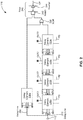
- FIG. 1 is a circuit diagram 100 of an example compensation circuit 110 in use with an example application circuit 120, in accordance with embodiments of the invention.
- the compensation circuit 110 takes a reference clock (REFCLK), input and ground voltages (V DD and V SS , respectively), power down (PD), reset (RSTN), test mode (TM), and frequency select (FS) signals.
- the reference clock signal may be any standard continuous clock signal.
- the power down signal when asserted, may indicate the compensation circuit is to be shut off; preferably, the power down signal is asserted high.
- the reset signal may reset the compensation circuit 110; preferably a reset occurs when the reset signal is asserted low while the reference clock signal is present.
- the frequency select signal may indicate an operating frequency for the application circuit.
- the compensation circuit 110 may assume the application circuit 120 is operating at a first operating frequency (e.g ., 133 MHz) when the frequency select signal is asserted low and a second operating frequency (e.g., 266 MHz) when the frequency select signal is asserted high.
- the compensation circuit 110 can therefore handle a range of reference clock frequencies (e.g ., 80MHz to 200 MHz).
- the test mode signal when asserted may indicate testing of the compensation circuit to determine the phase signals described below.
- the phase signals may be used to select an amount of phase offset for compensation.
- the four phase signals may be used as bits to enable coding of a selected phase offset.
- the phase signals PHO0 - PHO3 may be used to select a reference voltage for generation, as described below in more detail with respect to Figure 7 .
- a reference voltage offset may be determined.
- One method to determine the reference voltage offset is via a table lookup using the phase value as a key to a lookup table and then retrieving phase, frequency, and/or reference voltage offsets corresponding to the key.
- Other methods of determining phase, frequency and/or reference voltage offsets based on phase offset signals are possible as well.
- the compensation circuit 110 outputs a delay measure 118 that is input to the application circuit 120.
- the delay measure 118 is a current or voltage representing a PVT-compensation value of the reference clock REFCLK 112. Determination of the delay measure is described below with respect to Figure 3 .
- Figure 1 shows the application circuit 120 configured to output the delay measure 118 unchanged. Configuring the application circuit 120 to pass through the delay measure 118 permits by "daisy chaining" PVT-compensation data (i.e., the delay measure 118) through multiple application circuits.
- the compensation circuit 110 is designed to adjust for wide variations in voltage and temperature.
- the compensation circuit may have to compensate for input voltages that vary approximately 10% (e.g., 1.8 V ⁇ .15V or 2.5 V ⁇ 0.2V) and temperature ranges from -55°C to 125°C.
- the compensation circuit 110 is designed as well to account for process variations that arise either during fabrication or operation of the application circuit. Process variations that may occur during operation include, but are not limited to, Negative Bias Temperature Instability (NBTI), Hot Carrier Interactions (HCI) and/or Total Ionizing-radiation Dose (TID) effects. Further, process variations may arise more frequently during operation in the space environment than in a terrestrial environment, due to relatively-high radiation levels in the space environment.
- NBTI Negative Bias Temperature Instability
- HCI Hot Carrier Interactions
- TID Total Ionizing-radiation Dose
- Figure 1 shows an example application circuit 120 that, along with the delay measure 118, also takes input and ground voltages (V DD and V SS , respectively), a power down (PD) signal, and an input DQS (data strobe) signal 114 and generates outputs OUTO-OUT4.
- the application circuit 120 may take the input delay measure and apply it to an input signal, such as the DQS signal 114, to generate one or more outputs OUT0-OUT4 that correspond to the DQS signal 114 as compensated for PVT variations. Each of the outputs OUT0-OUT4 may correspond to different amounts of PVT-compensation.
- the application circuit can apply the delay measure to (clocked) input signals to generate PVT-compensated output(s) based on the input signal and the delay measure.
- the power down signal operates as described above with reference to the compensation circuit 110.
- the outputs OUT0-OUT4 may represent taps of the application circuit 120 with each separate output having a different delay.
- the compensation circuit 110 and/or the application circuit 120 may be implemented as an integrated circuit using a variety of technologies, such as CMOS, NMOS, or bipolar technologies.
- the compensation circuit 110 and/or the application circuit 120 may be packaged in an application-specific integrated circuit (ASIC) and/or as a macrocell of an ASIC.
- ASIC application-specific integrated circuit
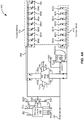
- FIG. 2 is a circuit diagram showing the example compensation circuit 110 in more detail, in accordance with embodiments of the invention.
- the compensation circuit 110 passes the REFCLK input 112 into two delay lines 200 and 210.
- Each delay line may have one or more delay elements;
- Figure 2 shows a first example delay line 200 with one delay element 202a and a second example delay line 210 with four example delay elements 220a, 220b, 220c, and 220d.
- Each of the unlabeled lines on Figure 2 connected to an electrical component pointing up may represent a V DD voltage input and each unlabeled line connected to an electrical component pointing down may represent a V SS voltage input.
- the compensation circuit may have a first delay line with m delay elements ( m > 0) and a second delay line with m + n ( n > 0) delay elements.
- the delay measure 118 may be based on comparing pulses of REFCLK 112 passing through each of the two delay lines.
- all of the delay elements 202a, 220a, 220b, 220c, and 220d on both delay lines 200 and 210 may be identical; that is, they may each have identical electrical components with each of the electrical components connected in the same fashion.
- Example embodiments of a delay element are discussed below with respect to Figure 3 .
- the delay elements 202a, 220a, 220b, 220c, and 220d may not be identical and/or all of the delay elements on a given delay line may be identical but may differ from the delay elements on the other delay line ( i.e., the delay elements 220a, 220b, 220c, and 220d may be identical and all differ from delay element 202a).
- one or more of the delay elements 202a, 220a, 220b, 220c, and 220d may be replaced by one or more other electronic components, such as an operational amplifier (op-amp).
- op-amp operational amplifier
- Figure 2 shows each delay element receiving three inputs: an input pulse based on the REFCLK and two input currents IBN and IBP. Each delay element may receive different inputs; Figure 2 shows that delay elements 202a, 220a, 220b, 220c, and 220e each receive separate IBP inputs IBP0, IBP1, IBP2, IBP3, IBP4, and IPB5, respectively, and separate IBN inputs IBN0, IBN1, IBN2, IBN3, IBN4, and IBN5, respectively.
- delay element 220a of delay line 210 may take REFCLK 112 as an input, and each successive delay element 220b, 220c, and 220d may take the output of the preceding delay element (220a, 220b, and 220c, respectively) as an input in place of the REFCLK 112 input of delay element 220a.
- the input currents to a delay element of delay line 200 may be adjusted based on the phase offset, reference voltage offset and/or frequency offsets as indicated by the phase signals discussed above with reference to Figure 1 .
- the delay measure 118 may be determined by combining and/or filtering pulses that pass or have passed through the delay lines 200 and 210.
- Figure 2 shows that output pulses of both the delay lines 200 and 210 are inputs to the XOR 230.
- XOR 230 performs an exclusive-or operation on its inputs to generate an offset pulse.
- the offset pulse may indicate where the pulse passing through delay line 200 is out of phase with the pulse passing through delay line 210.
- the output of XOR 230 may be filtered by filter 240, which takes the offset pulse output of XOR 230 and the pulse from delay line 200 as inputs, NAND's these inputs together using NAND gate 242, and then inverts the output of NAND gate 242 with inverter 244 to generate a filtered offset pulse OP.
- filter 240 may effectively logically AND the offset pulse and the output of delay line 200.
- the offset pulse OP may be input into a delay-measure circuit, such as delay-measure circuit 400 discussed below in more detail with respect to Figure 4A , to generate the delay measure 118.
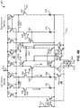
- FIG 3 is a circuit diagram showing an example delay element 300, in accordance with embodiments of the invention.
- the delay element 300 may be used as one or more of the delay elements in the compensation circuit 110 described above with respect to Figure 2 and/or in the application circuit 120 described below with respect to Figure 5 .
- Figure 3 shows the delay element 300 receiving power (V DD ) and ground voltage (V SS ) inputs, as well as a clock input pulse (IN). Additionally, the delay element 300 receives two current inputs (IBP and IBN). IBP and IBN may be the same current inputs as IBP and IBN described above with respect to Figure 2 .
- the power down (PD) input operates as a power down input for the delay element 300.
- Figure 3 shows the input currents and voltages are shown as mirrored between the two identical current-starved inverters 310 and 320.
- Each of the current-starved inverters 310 and 320 act to both delay and invert their input signals.
- current-starved inverter 310 takes input pulse IN as an input and generates an inverted and delayed copy of input pulse IN as an output ( e.g., as measured at node 325).
- Current-starved inverter 320 takes the output of current-starved inverter 310 as an input and generates output pulse OUT2 as an output.
- the logical value of the OUT2 output pulse i.e., "0" or "1" is the same as that of input pulse IN.
- Figure 3 shows each of the current-starved inverters 310 and 320 made up of 4 transistors: 312, 314, 316, and 318 for current-starved inverter 310 and 322, 324, 326, and 328 for current-starved inverter 320.
- current-starved mirror 310 is made up of PMOS transistors 312 and 314 and NMOS transistors 316 and 318.
- Transistor 312 has its source node connected to power V DD , its gate node connected to the IBP current input, and its drain node connected to the emitter node of transistor 314.
- the gate nodes of both transistors 314 and 316 are connected to input signal IN and the drain nodes of transistors 314 and 316 are connected together.
- the source node of transistor 316 is connected to the drain node of transistor 318.
- the gate node of transistor 318 is connected to the IBN current input 318 and the source node of transistor 318 is connected to ground V SS .
- the current-starved inverters 310 and 320 working in conjunction with transistors 302 and 304 may adjust the amount of delay incurred by signals passing from the input pulse IN to the output pulse OUT based on the currents IBP and IBN.
- Transistor 302 may adjust the delay of signals passing through the current-starved inverters 310 and 320 by limiting the current the current-starved inverters 310 and 320 can generate to drive the load following the respective current-starved inverter.
- transistor 304 may adjust the delay of signals passing through the current-starved inverters 310 and 320 by limiting the current the inventor each of the current-starved inverters 310 and 320 can generate to drive the load following the respective current-starved inverter.
- Figure 3 shows the output pulse OUT2 generated by current-starved inverter 320 passed on to two OR gates 340 and 342 connected in series, which act to shape output pulse OUT.
- OR gate 340 takes OUT2 and V SS (which acts as a logical "0") as logical inputs and generates output pulse OUT1.
- the effect of OR gate 340 is to generate OUT1 as a delayed version of OUT2 with the same logical value as OUT2.
- OR gate 342 takes OUT1 and V SS as logical inputs and generates output pulse OUT.
- the effect of OR gate 342 is to generate OUT as a delayed version of OUT1 with the same logical value as OUT.
- output pulses OUT and OUT2 are logically equivalent to, albeit delayed, input pulse IN.
- OR gates 340 and 342 may be replaced by other components, such as but not limited to appropriately configured groups (e.g ., pairs) of inverters, AND gates, NAND gates, or NOR gates to shape output pulses while ensuring the logical value of the output pulse OUT is not changed from that of output pulse OUT2.
- the net effect of the delay element 300 is to generate output pulses OUT and OUT2 that each correspond to a delayed and amplified version of input pulse IN.
- the delay buffer 300 may provide a generally uniform skew of OUT for circuits utilizing the output pulse OUT as a clock signal.
- Figure 4A is a circuit diagram showing an example delay-measure circuit 400, in accordance with embodiments of the invention. While shown separately herein, the example delay-measure circuit 400 may be part of the compensation circuit 110.
- the delay-measure circuit 400 takes offset pulse OP as input, such as offset pulses generated by the compensation circuit 200 described above with respect to Figure 2 , as well as bias current I BIAS and determines delay measure DM by using differential amplifier 420 ("Diff Amp") to average the duty cycle value of OP and scale a reference voltage VREF by the average duty cycle value.
- the differential amplifier 420 generates output signals IPOS and INEG from inputs + IN which is based on input signal OP, - IN which is based upon VREF, V DD , V SS , I BIAS , PD, and FS.
- the reference-voltage generator 700 generates VREF as an output from inputs V DD , V SS , PHO0, PHO1, PHO2. and PHO3.
- the differential amplifier 420 is described below in more detail with respect to Figure 4B and the reference-voltage generator 700 is described below in more detail with respect to Figure 7 .
- the delay measure may be output either as a single output or as multiple outputs.
- Figure 4A shows a current mirror 410 with 8 outputs: IBN0, IBN1, IBN2, IBN3, IBN4, IBN5, IBN6, and DM.
- a separate current mirror may provide corresponding taps for positive voltage inputs.
- Figure 4A shows a current mirror 412 with 7 outputs: IBP0, IBP1, IBP2, IBP3, IBP4, IBP5, and IBP6.
- Each of the outputs IBN0-IBN6 and DM may have the same current and voltage, and each of the outputs IBP0-IBP6 may have the same current and voltage as well, while the voltage and current of outputs IBN0-IBN6 and DM may differ from the current and voltage of the outputs IBP0-IBP6.
- the delay measure DM may be output as one or more currents. Further, the delay measure DM may be passed on to additional application circuits, permitting daisy-chaining of PVT compensation as described above with respect to Figure 1 .
- the delay-measure circuit 400 may be a ratiometric circuit configured to determine an average width or duty cycle of OP by averaging the width of pulses received as input OP acting as input + IN to loop amplifier 420 relative to the reference voltage VREF acting as input -IN to loop amplifier 420.
- Figure 4A shows delay-measure circuit 400 with startup circuit 490.
- the startup circuit 490 may bring up the delay-measure circuit 400 after a reset and/or upon powering the delay-measure circuit.
- Figure 4A shows the startup circuit 490 with V DD , Vss, a negated power down signal PD , and PHO1, PHO2, and PHO3 signals as inputs and configured to generate an output signal OUT.
- the startup circuit 490 is described in more detail below with respect to Figure 4C .
- the output signal OUT of startup circuit 490 may be passed on to a transmission gate 402.
- the transmission gate 402 may pass the output signal OUT to the remainder of the delay-measure circuit when the RST signal is high; otherwise the output signal OUT may not be passed on to the reminder of the delay-measure circuit.
- the output signal OUT is only passed on when the delay-measure circuit 400 is being reset as indicated when the reset signal RST is high.
- Figure 4B is a circuit diagram showing an example differential amplifier 420, in accordance with embodiments of the invention.
- the differential amplifier 420 takes the inputs and generates the outputs described above with respect to Figure 4A .
- Figure 4B shows the + IN input passed into transistors 438 and 448 and the - IN input passed into transistors 442 and 452.
- the difference between the +IN input and -IN input may be multiplied by the differential amplifier 420 and provided as the IPOS and INEG outputs.
- the loop amplifier 420 compares the average width of the pulses of the +IN input relative to a reference voltage at the -IN input.
- Transistors 430 and 476 are used to implement a power down state when the power down PD signal is high.
- Figure 4B shows the differential amplifier 420 with two current sources: a left current source and a right current source.
- the left current source includes PMOS transistors 424, 426, 438, and 442 and resistors 440, 464, and 466.
- the source nodes of transistors 424 and 426 are connected to V DD
- the gate nodes of transistor 424 and 426 are connected to the I BIAS input
- the drain nodes of transistors 424 and 426 are both connected to resistor 440.
- the drain node of transistor 424 is also connected to the source node of transistor 438
- the gate node of transistor 438 is connected to the + IN input and the drain node of transistor 438 is connected to resistor 464.
- the drain node of transistor 426 is also connected to the source node of transistor 442, the gate node of transistor 442 is connected to the - IN input and the drain node of transistor 442 is connected to resistor 466.
- the output of the left current source may be taken at node 453.
- the output of the left current source is then passed to the gate node of PMOS transistor 454.
- Transistor 454 may allow current to flow from the drain node output of transistor 428 toward V SS (and then through gate node of NMOS transistor 444) when the output of the left current source provides a current to transistor 454.
- the IPOS output is then at the source node of transistor 444.
- Right current source is connected in a similar fashion with transistors 434, 436, 448, and 452 respectively corresponding to transistors 424, 426, 438, and 442 of left current source and resistors 450, 472, and 474 of right current source respectively corresponding to resistors 440, 464, and 466 of left current source.
- the output of right current source may be taken at node 457.
- the gate node of transistor 448 receives the + IN input (as opposed to the -IN input received at the gate node of transistor 442)
- the output of the right current source at node 457 may depend on the +IN input (and therefore the INEG output from the source node of NMOS transistor 446) rather than the -IN input of the left current source.
- the IPOS and INEG outputs may also have reverse polarities.
- the transmission gate 484 and transistors 460, 462, 468, 470, 478, 480, and 482 are used to implement a gain of the difference between IPOS and INEG outputs when the FS input is set high and therefore the negated FS input FS is set low.
- the gain may be two; that is, the difference between IPOS and INEG may be doubled when FS is set high.
- the differential amplifier 440 may provide a corresponding output for a base reference clock frequency when the FS input set low and a doubled output for the doubled reference clock frequency when the FS input set high.
- Figure 4C is a circuit diagram showing an example startup circuit 490, in accordance with embodiments of the invention.
- Figure 4C shows the startup circuit 490 with V DD , Vss, a negated power down signal PD , and PHO1, PHO2, and PHO3 signals as inputs and configured to generate an output signal OUT.
- Each of the unlabeled lines on Figure 4C connected to an electrical component pointing up may represent a V DD voltage input and each unlabeled line connected to an electrical component pointing down may represent a V SS voltage input.
- Figure 4C shows the negated power down signal PD passed on to inverter 491, which then generates the non-negated power down signal PD.
- PD is also passed on to components 492 and 493 which permit signals to pass when PD is set high (that is, when PD is set low).
- the PD signal is also provided to the gate node of NPN transistor 494 which then controls current flow from input with V DD to Vss and to the remainder of the startup circuit.
- the output signal OUT may not be generated when PD is set high (or correspondingly when PD is set low).
- Figure 4C shows that the output signal OUT may be generated when either the A, B, C, or D inputs is logically high to permit respective transmission gates 495, 496, 497 or 498 to allow current flow.
- the logic shown on the right hand side of Figure 4C may be used to generate the A, AN, B, BN, C, CN, D, and DN inputs to the transmission gates 495, 496, 497, and 498.
- Figure 4C shows the PHO1, PHO2, and PHO3 input signals are each inverted by inverters 495a, 495b, and 495c.
- Figure 4C shows the negated PHO 1 , PHO 2 , and PHO 3 input signals passed into NAND gate 495d which then generates the AN input.
- the AN input is then negated by inverter 495e to generate the A input.
- input AN may be set high and corresponding input A set low unless PHO1, PHO2, and PHO3 are set high. If PHO1, PHO2, and PHO3 are all high, though, input A may be set high and input AN may be set low.
- a test mode may signaled using one of the combinations of the PHO1, PHO2, and PHO3 inputs that leads to generation of the OUT output being generated by the startup circuit 490 (e.g., a test mode may be signaled with PHO1 set high, PHO2 set low, and PHO3 set low to generate the B output and thus cause transmission gate 496 to allow current flow for the OUT output).
- the OUT output may provide current to bias components of the delay-measure circuit 400; i.e., the OUT output may drive current mirrors 410 and 420 to generate the various IBN and IBP outputs that power the various delay elements in the compensation circuit 110 and/or the application circuit 120.
- the compensation circuit 110 and/or the application circuit may be biased while awaiting for reset of other circuits, such as phase-locked loops (PLLs), that may require a relatively long period of start up time (e.g. , 250 ⁇ s or more), and to therefore reduce the time required to provide PVT-compensation to a few additional percent of a total reset time budget (e.g. , less than 10 additional ⁇ s, which is equivalent to adding 4% or less of a reset time budget based on a 250 ⁇ s reset for other circuitry).
- PLLs phase-locked loops
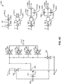
- Figure 5 is a circuit diagram showing an example application circuit 500, in accordance with embodiments of the invention.
- the example application circuit 500 may be used to test the compensation circuit 110 and/or may take the place of application circuit 120 discussed above with respect to Figure 1 .
- the example application circuit 500 receives a strobe input DQS 114.
- DQS 114 may represent a data strobe input.
- the data strobe input may have a pulse each time a memory operation, such as a read or a write operation, is to be performed.
- Memory operations may be timed based on rising or falling edges of the data strobe input.
- FIG. 5 shows the application circuit 500 with five delay elements 510, 520, 530, 540, and 550.
- Example embodiments of a delay element are discussed above with respect to Figure 3 .
- Each delay element may receive one or more currents or voltages corresponding to the delay measure DM.
- Figure 5 shows each delay element 510, 520, 530, 540, and 550 receiving two input currents: a positive current IBP0, IBP1, IBP2, IBP3, or IBP4, respectively, and a negative current IBN0, IBN1, IBN2, IBN3, or IBN4, respectively. More or fewer delay elements may be used in the application circuit 550.
- negative and positive currents may be the currents shown in Figure 4 as generated by the current mirrors 420 and 430, respectively.
- the negative current may explicitly represent the delay measure DM and the positive current may represent the reference voltage VREF.
- Figure 5 shows each of the delay elements 510, 520, 530, 540, and 550 as identical.
- the delay elements 510, 520, 530, 540, and 550 may not be identical.
- one or more of the delay elements 510, 520, 530, 540, and 550 may be replaced by one or more other electronic components, such as an operational amplifier (op-amp).
- op-amp operational amplifier
- Figure 5 also shows the application circuit 500 with five taps: 512, 522, 532, 542, and 552.
- Each of the taps may be used to convey one or more outputs from the one or more delay elements; that is, taps 512, 522, 532, 542, and 552 may convey one or more outputs from delay elements 510, 520, 530, 540, and 550, respectively.
- one or more other application circuit(s) may replace the example application circuit 120.
- Each of the outputs at taps 512, 522, 532, 542, and 552 may represent PVT-compensated outputs corresponding to the DQS input 114.
- each output of the outputs at taps 512, 522, 532, 542, and 552 may include a successively longer delay as part of the PVT compensation.
- more or fewer taps may be used in an application circuit 500 than shown in Figure 5 .
- the application circuit 500 may be used as a component in a larger application circuit.
- the larger application circuit may use the application circuit 500 as a "front end" or “back end "to PVT-compensate a respective input signal or output signal, respectively.
- a DRAM may include the application circuit 500 as a front-end to PVT-compensate a DQS signal before using the compensated-data-strobe signal to operate the DRAM.
- a memory controller or other device that generates data strobe signals as outputs may use the application circuit to PVT-compensate the output data strobe signals.
- Choice of a specific tap (i.e., a specific amount of delay) to use for the compensated-data-strobe signal may be determined at design or during operation. Many other examples of combining application circuit 500 with other application circuits are possible as well.
- application circuits include, but are not limited to, memory circuits (e.g., DRAMs and synchronous DRAMs (SDRAMs)), processor circuits, control circuitry, and/or driver circuits.
- the application circuit may be a DRAM or an SDRAM, and may be configured to comply to one or more DRAM standards, such as but not limited to DDR, DDR2, and/or DDR3 standards.
- any clocked circuit such as but not limited to processors and control logic circuits, could readily be used as an application circuit.
- a memory-bus driver such as described below with respect to Figure 6 , may be used as an application circuit as well.
- FIG. 6 is a memory-bus driver 600, in accordance with embodiments of the invention.
- the memory-bus driver 600 may be used as an application circuit as described above with respect to Figures 1 and 5 .
- the memory-bus driver 600 may be used to interface with a DRAM.
- the DRAM may be an SDRAM, such as a DRAM configured to meet the DDR, DDR2, and/or DDR3 standards.
- the compensation circuit 110 is shown in the center of Figure 6 with cross-hatching. The remainder of the circuit shown in Figure 6 corresponds to the application circuit 120 described above in Figure 1 .
- the memory-bus driver 600 is divided into two domains or regions where a particular clock signal is operative.
- the CLK1X domain (divided into two portions by dashed lines as shown in Figure 6 ) indicates regions of the memory-bus driver where the CLK1X signal synchronizes operations.
- the DQS domain indicates regions of the memory-bus driver where the DQS signal synchronizes operations.
- the memory-bus driver may be used in association with a memory (not shown), such as a DRAM.
- the DO[7:0], D1[7:0], and DQ[7:0] lines may be data lines where the [7:0] nomenclature indicates that 8 lines are used.
- the D0[7:0] lines includes 8 lines: D0[0], DO[1], D0[2], D0[3], D0[4], D0[5], D0[6], and D0[7].
- the DQSTX line may be used as a strobe signal to indicate data is to be transmitted from the associated memory.
- the DQ[7:0] lines may be used to receive and/or transmit data to the memory-bus driver.
- the DQS line may be asserted when data is present on the DQ[7:0] lines.
- the VREF line may carry a reference voltage, such as described above with respect to Figure 4 and/or as described below with respect to Figure 6 .
- the PHO[3:0] lines may be carry the phase signals described above with respect to Figures 1 and below with respect to Figure 7 .
- the power down PD line may carry a power down signal to disable the memory-bus driver 600, such as the power down signal described above with respect to Figures 1 and 2 .
- the READCMD line may include a signal indicating if a read operation or a write operation is to be performed by the associated memory.
- the RSTN line may carry a reset signal such as described above with respect to Figure 1 .
- the CLK1X line may carry a clock signal operating at a known frequency, such as 100 MHz or 133.33 MHz.
- the CLK1XN90 line may carry a signal representing a phase shifted version of the CLK1X signal, such as a 90° phase-shifted signal from the CLK1X signal.
- the CLK2X line may carry a signal representing a multiplied clock signal; that is a clock signal whose frequency is a multiple of the CLK1X line, where the multiple may be two, three, or another integer number. As indicated in Figure 6 , the multiple for the CLK2X line is two.
- the RXCLKSEL may enable selection of a clock signal, such as selection of either the signal on the CLK1X line or the signal on the CLK1XN90 line.
- the CASLAT[1:0] lines may be two lines (CASLAT[0] and CASLAT[1]) each carrying a signal indicating a column address strobe (CAS) latency amount.
- the RDVALID line may carry a signal indicating whether the read operation is valid.
- the RDELAY[1:0] (RDELAY[0] and RDELAY[1]) lines may be two lines indicating a read delay amount.
- the memory-bus driver 600 may be used to control either write or read operations with the associated memory.
- To perform a write operation whose data arrives on data lines DO[7:0] and D1[7:0] to be written to the memory via the DQ[7:0] lines half of the data D0/D1 lines (that is, either data lines D0[0:7] or D1[0:7]) may be selected using multiplexer (MUX) 602.
- MUX 602 may be passed into toggle flip-flop (TFF) 604.
- TFF 604 shown as DQO[7:0]
- the DQSO signal may be generated based on passing a signal from the DQSTX line through TFF 606, which is then sent on the DQS line to the associated memory.
- the DQSTX signal may be input via the DQS line, and latched using TFF 624 and then passed into the compensation circuit 110 as the frequency select (FS) signal.
- the input data shown as DQRX[7:0] in Figure 6 presented from the DQ[7:0] lines may be latched by TFF 614.
- the TFFs 614 and 624 may use the STROBE_ENABLE signal logically OR'd with the DQS_DLY signal via OR gates 616 and 626, respectively, as a clock signal.
- the DQS_DLY signal may represent the output delay measure of the compensation circuit 110.
- the input data may be stored in the elasticity buffer 618 as described above.
- a specific per-operation buffer of the elasticity buffer 618 may be selected using the 1:4 MUX 632 controlled by three-bit counter 634 that is clocked using the DQS_DLY signal output from the compensation circuit 110.
- the output of the three-bit counter 634 shown as WPTR on Figure 6 , is also passed on to TFF 636 to generate a ready signal, indicating the elasticity buffer 618 has storage for more data, and a full signal, indicating the elasticity pointer is completely occupied.
- the WPTR signal may select a per-operation buffer of the elasticity buffer 618 to be output for write operations.
- the selection of a specific per-operation buffer of the elasticity buffer 618 for read operations is controlled using signals on the CASLAT[1:0] lines passed into the CAS latency TFFs 642.
- the CAS latency TFFs 642 are clocked by signals on either the CLK1X line or the CLK1XN90 line as selected using signals on the RXCLKSEL line via MUX 640.
- the CAS latency TFFs 642 generate four outputs, one of which is selected by the MUX 644 using the two CASLAT[1:0] lines as control signals.
- the output of the MUX 644, shown in Figure 6 as STROBE_ENABLE, is passed into the TFFs 650, 652, 654, 656, which latch the STROBE_ENABLE signal over four clock cycles.
- the TFFs 650, 652, 654, and 656 as well as three-bit counter 662 are clocked using signals on the CLK1X line.
- the outputs of TFFs 652, 654, and 656, along signals on the RDVALID line are passed into MUX 660, which generates one output as controlled by control signals from the RDELAY[1:0] lines.
- the output of the MUX 660 is passed into a three-bit counter 662 which generates a signal, shown as RPTR on Figure 6 , used to control MUX 630.
- the RPTR signal may select a per-operation buffer of the elasticity buffer 618 to be output for read operations.
- the WPTR signal may be used to select a per-operation buffer of the elasticity buffer 618
- Figure 7 is a circuit diagram showing an example reference-voltage generator 700 for generating a reference voltage, in accordance with embodiments of the invention.
- the example reference-voltage generator 700 takes as inputs the phase signals PHO1, PHO2, and PHO3 described above with respect to Figures 1 and 4A .
- the phase signals PHO0, PHO1, PHO2, and PHO3 may be passed into a 4-to-16 decoder 710. Only fifteen of the 16 output lines L0-L15 of the 4-to-16 decoder 710 are shown, due to space restrictions.
- the phase signals may be interpreted as binary digits to indicate a particular reference voltage to be generated.
- the signals may be processed such that PHO3 signal is interpreted as a most significant digit of a four-bit binary number, PHO2 as the second-most significant digit, PHO1 as the third-most significant digit, and PHO0 as the least significant digit (or vice versa).
- PHO3 signal is interpreted as a most significant digit of a four-bit binary number
- PHO2 the second-most significant digit
- PHO1 the third-most significant digit
- PHO0 the least significant digit (or vice versa).
- the 4-to-16 decoder may activate exactly one of the output lines L0...L15 based on the phase signal inputs and may deactivate the remaining output lines. For example, if the PHO3 and PHO2 signals are set high and the PHO1 and PHO0 signals are set low, output line L12 (corresponding to reference voltage 12) may be activated.
- a signal on the activated line may be used to open a first corresponding transmission gate; that is one of transmission gates 740a-740o (transmission gate 740p not shown) and a second corresponding transmission gate 750a-750o (transmission gate 750p not shown). Then, a current at a known voltage, such as V DD , may pass through a corresponding resistor R720-R734 (R735 not shown), and then through a second corresponding transmission gate 750a-750o (transmission gate 750p not shown), before being output as a reference voltage VREF.
- Each of the deactivated lines may not open their corresponding transmission gates to allow current to flow, and thus an output voltage may not be generated for each of the deactivated line.
- Each of the resistors R720-R735 may have a different resistance value, leading to a different reference voltage for each of the sixteen possible activated lines.
- the phase signals PHO0-PHO3 are used to determine one of sixteen possible reference voltage VREF outputs by the reference-voltage generator 700. More or fewer possible reference voltages may be output by the reference-voltage generator 700 based on a corresponding addition or deletion of phase signals, transmission gates, and/or resistances.
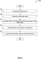
- FIG. 8 is a flow chart of an example method 800 for generating a delay measure to compensate for PVT variations in an application circuit, in accordance with embodiments of the invention.
- each block in this flowchart presented herein may represent a module, segment, or combination of electronic components, perhaps executing computer firmware and/or software, for implementing specific logical functions or steps in the process. Alternate implementations are included within the scope of the example embodiments in which the blocks described herein may be executed out of order from that shown or discussed, including substantially concurrently or in reverse order, depending on the functionality involved, as would be understood by those reasonably skilled in the art of the described embodiments.
- Method 800 begins at block 810.
- a first delay output is generated.
- the first delay output may be generated by a first delay line.
- the first delay line may include m delay elements, where m is an integer greater than 0.
- the m delay elements may be connected together to form the delay line.
- each of the m delay elements may be identical, such as each being delay elements as shown in Figure 3 or delay buffers as shown in Figure 4 .
- the first delay line may accept one or more inputs.
- the inputs may include power VDD and ground VSS voltages as well as a reference clock input.
- the inputs may include one or more input currents, such as IBP and IBN discussed above with respect to Figures 3 and 4 .
- each of the delay elements of the first delay line may be identical as discussed above, each delay element may receive different inputs, such as receiving different input currents and/or different reference clock inputs.
- some inputs, such as the voltage inputs may be common between all delay elements in the first delay line.
- the first delay output may be generated based on these inputs, as discussed above with respect to Figures 3 and 4 .
- the first delay line may be on an integrated circuit.
- the integrated circuit may be implemented using Negative Metal Oxide Silicon (NMOS), Complementary Metal Oxide Silicon (CMOS), bipolar or one or more other technologies.
- NMOS Negative Metal Oxide Silicon
- CMOS Complementary Metal Oxide Silicon
- bipolar bipolar or one or more other technologies.
- a second delay output is generated.
- the first delay output may be generated by a second delay line.
- the first delay line may include m + n delay elements, where m is as described above with respect to block 810 and n is an integer greater than 0.
- the delay elements of the second delay line may have the characteristics of the delay elements described above with respect to block 810. Further, each of the delay elements of the first delay line and of the second delay line may be identical; i.e. , the two delay lines together may contain 2 * m + n identical delay elements.
- the inputs and outputs of the second delay line may share the characteristics of the inputs and outputs of the first delay line discussed above with respect to block 810.
- the two delay lines may be part of a compensation circuit, such as described above with respect to Figures 1-4 and 6 .
- the second delay line and/or the compensation circuit may be on an integrated circuit, such as described above with respect to block 810.
- an offset pulse may be generated based on the first delay output and the second delay output.
- the offset pulse may be generated based on performing an XOR operation on the first delay output and the second delay output.
- the output of the XOR operation may be filtered.
- the XOR output may be NAND'd with either the first delay output or the second delay output and then inverted, effectively AND'ing the XOR output and the chosen delay output.
- a delay measure may be generated based on the offset pulse.
- the delay measure may be based on determining a width or duty cycle of the offset pulse averaged over time.
- the delay measure may then be the average voltage of the offset pulse, perhaps provided as one or more currents and/or voltages.
- the voltages may be direct current (DC) voltages.
- a delay-measure circuit may be used to generate the delay measure from an input offset pulse.
- the delay measure may be determined relative to a reference voltage.
- the delay-measure circuit may be ratiometric and/or include an differential amplifier.
- the delay measure may be a current or voltage corresponding to a process, voltage, and temperature (PVT) compensation for the reference clock signal.
- PVT process, voltage, and temperature
- the delay measure may be output to an application circuit.
- the application circuit may take the delay measure (either current or voltage) output from the compensation circuit.
- the delay measure may be input as one or more currents to PVT-compensate a input signal of the application circuit, such as described above with respect to the DQS signal of Figure 5 .
- the application circuit may be a test application circuit, such as the example application circuit shown above with respect to Figure 5 , or a memory-bus driver, such as shown above with respect to Figure 6 .
- the application circuit may also or instead be any circuit that takes a clock signal as input, such as but not limited to one or more random access memories (RAMs) (e.g., a DRAM and/or an SDRAM), one or more processor circuits, one or more control circuits, and/or one or more timing circuits.
- RAMs random access memories
- the application circuit may use the example application circuit shown in Figure 5 as a front end or back end to PVT-compensate respective input or output signals.
- Application circuits may pass through delay measure signals unchanged to permit daisy-chaining of PVT compensation to multiple application circuits. Many other types of application circuits are possible as well.
Landscapes
- Engineering & Computer Science (AREA)
- Microelectronics & Electronic Packaging (AREA)
- Computer Hardware Design (AREA)
- Physics & Mathematics (AREA)
- Nonlinear Science (AREA)
- Pulse Circuits (AREA)
- Stabilization Of Oscillater, Synchronisation, Frequency Synthesizers (AREA)
- Dram (AREA)
- Logic Circuits (AREA)
Applications Claiming Priority (1)
| Application Number | Priority Date | Filing Date | Title |
|---|---|---|---|
| US12/418,981 US8390352B2 (en) | 2009-04-06 | 2009-04-06 | Apparatus and method for compensating for process, voltage, and temperature variation of the time delay of a digital delay line |
Publications (3)
| Publication Number | Publication Date |
|---|---|
| EP2239849A2 EP2239849A2 (en) | 2010-10-13 |
| EP2239849A3 EP2239849A3 (en) | 2013-12-18 |
| EP2239849B1 true EP2239849B1 (en) | 2018-03-14 |
Family
ID=42537943
Family Applications (1)
| Application Number | Title | Priority Date | Filing Date |
|---|---|---|---|
| EP10152009.6A Not-in-force EP2239849B1 (en) | 2009-04-06 | 2010-01-28 | Apparatus and method for compensating for process, voltage, and temperature variation of the time delay of a digital delay line |
Country Status (4)
| Country | Link |
|---|---|
| US (1) | US8390352B2 (enExample) |
| EP (1) | EP2239849B1 (enExample) |
| JP (1) | JP5421142B2 (enExample) |
| TW (1) | TWI525997B (enExample) |
Families Citing this family (21)
| Publication number | Priority date | Publication date | Assignee | Title |
|---|---|---|---|---|
| US8390356B2 (en) * | 2008-05-08 | 2013-03-05 | Kpit Cummins Infosystems, Ltd. | Method and system for open loop compensation of delay variations in a delay line |
| US20130015837A1 (en) * | 2011-07-13 | 2013-01-17 | International Business Machines Corporation | On-chip signal waveform measurement circuit |
| US8850155B2 (en) * | 2011-12-19 | 2014-09-30 | Advanced Micro Devices, Inc. | DDR 2D Vref training |
| CN107092383B (zh) * | 2012-03-29 | 2020-09-11 | 禾瑞亚科技股份有限公司 | 触摸处理器 |
| US8742815B2 (en) * | 2012-06-20 | 2014-06-03 | Qualcomm Incorporated | Temperature-independent oscillators and delay elements |
| US8867595B1 (en) | 2012-06-25 | 2014-10-21 | Rambus Inc. | Reference voltage generation and calibration for single-ended signaling |
| US9503088B2 (en) | 2013-01-10 | 2016-11-22 | Freescale Semiconductor, Inc. | Method and control device for recovering NBTI/PBTI related parameter degradation in MOSFET devices |
| WO2014210192A1 (en) * | 2013-06-25 | 2014-12-31 | Ess Technology, Inc. | Delay circuit independent of supply voltage |
| KR20160009429A (ko) * | 2014-07-16 | 2016-01-26 | 삼성전자주식회사 | Pvt 변동에 둔감한 딜레이 컨트롤 시스템 및 그 제어 방법 |
| CN105049043B (zh) * | 2015-06-30 | 2018-05-08 | 北京时代民芯科技有限公司 | 一种带有失调校正功能的高速比较器 |
| KR102424896B1 (ko) * | 2016-02-25 | 2022-07-26 | 에스케이하이닉스 주식회사 | 데이터 트레이닝 장치 및 이를 포함하는 반도체 장치 |
| US9792964B1 (en) * | 2016-09-20 | 2017-10-17 | Micron Technology, Inc. | Apparatus of offset voltage adjustment in input buffer |
| CN106847319B (zh) * | 2016-12-23 | 2021-06-29 | 深圳市紫光同创电子有限公司 | 一种fpga电路及窗口信号调整方法 |
| CN108806744B (zh) * | 2017-05-05 | 2020-11-27 | 中芯国际集成电路制造(上海)有限公司 | 一种延时产生电路及非易失性存储器读时序产生电路 |
| CN107315442B (zh) | 2017-06-30 | 2019-04-30 | 上海兆芯集成电路有限公司 | 控制器与参考电压产生方法 |
| CN107342766B (zh) * | 2017-09-02 | 2023-08-11 | 合肥学院 | 一种近阈值电压全数字逐次逼近寄存器延时锁定环系统 |
| CN109900971B (zh) * | 2017-12-11 | 2023-01-24 | 长鑫存储技术有限公司 | 脉冲信号的处理方法、装置以及半导体存储器 |
| CN112152596B (zh) * | 2019-06-27 | 2024-03-08 | 台湾积体电路制造股份有限公司 | 用于产生脉冲输出的电路及方法 |
| CN111327298B (zh) * | 2020-03-12 | 2021-03-30 | 湖南毂梁微电子有限公司 | 一种超高精度数字脉冲信号产生电路及方法 |
| US10911035B1 (en) | 2020-05-04 | 2021-02-02 | Nxp Usa, Inc. | Fixed-width pulse generator |
| US20230141595A1 (en) * | 2021-11-08 | 2023-05-11 | Advanced Micro Devices, Inc. | Compensation methods for voltage and temperature (vt) drift of memory interfaces |
Citations (1)
| Publication number | Priority date | Publication date | Assignee | Title |
|---|---|---|---|---|
| JPS6369315A (ja) * | 1986-09-11 | 1988-03-29 | Sony Corp | Cmos回路を用いた可変遅延装置 |
Family Cites Families (42)
| Publication number | Priority date | Publication date | Assignee | Title |
|---|---|---|---|---|
| US4639688A (en) * | 1985-04-18 | 1987-01-27 | The United States Of America As Represented By The Secretary Of The Air Force | Wide-band phase locked loop amplifier apparatus |
| EP0236525B1 (de) * | 1986-03-12 | 1990-12-19 | Deutsche ITT Industries GmbH | Integrierte Isolierschicht-Feldeffekttransistor-Verzögerungsleitung für Digitalsignale |
| US4847870A (en) * | 1987-11-25 | 1989-07-11 | Siemens Transmission Systems, Inc. | High resolution digital phase-lock loop circuit |
| US4845388A (en) * | 1988-01-20 | 1989-07-04 | Martin Marietta Corporation | TTL-CMOS input buffer |
| US5101117A (en) * | 1988-02-17 | 1992-03-31 | Mips Computer Systems | Variable delay line phase-locked loop circuit synchronization system |
| US5021684A (en) * | 1989-11-09 | 1991-06-04 | Intel Corporation | Process, supply, temperature compensating CMOS output buffer |
| US5192886A (en) | 1990-03-15 | 1993-03-09 | Hewlett-Packard Company | Sub-nanosecond calibrated delay line structure |
| JP3091502B2 (ja) * | 1990-03-15 | 2000-09-25 | ヒューレット・パッカード・カンパニー | サブナノ秒較正遅延線構造 |
| JP3561792B2 (ja) * | 1995-09-06 | 2004-09-02 | 株式会社ルネサステクノロジ | クロック発生回路 |
| US5666322A (en) * | 1995-09-21 | 1997-09-09 | Nec Electronics, Inc. | Phase-locked loop timing controller in an integrated circuit memory |
| DE69839112T2 (de) * | 1997-12-19 | 2008-05-21 | Matsushita Electric Industrial Co., Ltd., Kadoma | Kammfilter und Steuerverfahren dazu |
| US5963071A (en) * | 1998-01-22 | 1999-10-05 | Nanoamp Solutions, Inc. | Frequency doubler with adjustable duty cycle |
| US6091271A (en) * | 1998-06-30 | 2000-07-18 | Lucent Technologies, Inc. | Frequency doubling method and apparatus |
| US6288587B1 (en) * | 1999-04-07 | 2001-09-11 | National Science Council Of Republic Of China | CMOS pulse shrinking delay element with deep subnanosecond resolution |
| US6316987B1 (en) * | 1999-10-22 | 2001-11-13 | Velio Communications, Inc. | Low-power low-jitter variable delay timing circuit |
| US6377103B1 (en) * | 2000-06-28 | 2002-04-23 | Intel Corporation | Symmetric, voltage-controlled CMOS delay cell with closed-loop replica bias |
| US6535735B2 (en) * | 2001-03-22 | 2003-03-18 | Skyworks Solutions, Inc. | Critical path adaptive power control |
| US6581017B2 (en) * | 2001-06-28 | 2003-06-17 | Intel Corporation | System and method for minimizing delay variation in double data rate strobes |
| US6918048B2 (en) * | 2001-06-28 | 2005-07-12 | Intel Corporation | System and method for delaying a strobe signal based on a slave delay base and a master delay adjustment |
| CN1393992A (zh) * | 2001-07-02 | 2003-01-29 | 朗迅科技公司 | 包含反馈回路的延迟补偿电路 |
| US6747500B2 (en) * | 2001-10-19 | 2004-06-08 | Mitutoyo Corporation | Compact delay circuit for CMOS integrated circuits used in low voltage low power devices |
| US6741522B1 (en) * | 2001-11-27 | 2004-05-25 | Lsi Logic Corporation | Methods and structure for using a higher frequency clock to shorten a master delay line |
| US7015740B1 (en) * | 2002-10-28 | 2006-03-21 | Cisco Technology, Inc. | Self-adjusting programmable on-chip clock aligner |
| US6801028B2 (en) * | 2002-11-14 | 2004-10-05 | Fyre Storm, Inc. | Phase locked looped based digital pulse converter |
| US6853231B2 (en) * | 2003-03-31 | 2005-02-08 | Mosaid Technologies Incorporated | Timing vernier using a delay locked loop |
| US7266739B2 (en) * | 2003-05-07 | 2007-09-04 | Credence Systems Solutions | Systems and methods associated with test equipment |
| US6940768B2 (en) * | 2003-11-04 | 2005-09-06 | Agere Systems Inc. | Programmable data strobe offset with DLL for double data rate (DDR) RAM memory |
| JPWO2005050844A1 (ja) * | 2003-11-20 | 2007-06-14 | 株式会社アドバンテスト | 可変遅延回路 |
| US7178048B2 (en) * | 2003-12-23 | 2007-02-13 | Hewlett-Packard Development Company, L.P. | System and method for signal synchronization based on plural clock signals |
| JP2006039830A (ja) * | 2004-07-26 | 2006-02-09 | Renesas Technology Corp | 半導体集積回路 |
| US7129763B1 (en) * | 2004-11-08 | 2006-10-31 | Western Digital Technologies, Inc. | Adjusting power consumption of digital circuitry by generating frequency error representing error in propagation delay |
| US7634039B2 (en) * | 2005-02-04 | 2009-12-15 | True Circuits, Inc. | Delay-locked loop with dynamically biased charge pump |
| US7123103B1 (en) * | 2005-03-31 | 2006-10-17 | Conexant Systems, Inc. | Systems and method for automatic quadrature phase imbalance compensation using a delay locked loop |
| US7388419B2 (en) * | 2005-07-22 | 2008-06-17 | Freescale Semiconductor, Inc | PVT variation detection and compensation circuit |
| US7222036B1 (en) * | 2006-03-31 | 2007-05-22 | Altera Corporation | Method for providing PVT compensation |
| KR100776903B1 (ko) * | 2006-04-24 | 2007-11-19 | 주식회사 하이닉스반도체 | 지연 고정 루프 |
| US7433262B2 (en) * | 2006-08-22 | 2008-10-07 | Atmel Corporation | Circuits to delay a signal from DDR-SDRAM memory device including an automatic phase error correction |
| JP2008078995A (ja) * | 2006-09-21 | 2008-04-03 | Nec Electronics Corp | 移相回路 |
| JP4892402B2 (ja) * | 2007-04-25 | 2012-03-07 | ルネサスエレクトロニクス株式会社 | 半導体集積回路装置 |
| JP2009017151A (ja) * | 2007-07-04 | 2009-01-22 | Yokogawa Electric Corp | 遅延回路およびそれを用いた信号発生回路 |
| JP5451012B2 (ja) * | 2008-09-04 | 2014-03-26 | ピーエスフォー ルクスコ エスエイアールエル | Dll回路及びその制御方法 |
| KR100985413B1 (ko) * | 2008-10-14 | 2010-10-06 | 주식회사 하이닉스반도체 | 지연회로 및 그를 포함하는 지연고정루프회로 |
-
2009
- 2009-04-06 US US12/418,981 patent/US8390352B2/en not_active Expired - Fee Related
-
2010
- 2010-01-28 EP EP10152009.6A patent/EP2239849B1/en not_active Not-in-force
- 2010-02-05 TW TW099103608A patent/TWI525997B/zh not_active IP Right Cessation
- 2010-02-05 JP JP2010024183A patent/JP5421142B2/ja not_active Expired - Fee Related
Patent Citations (1)
| Publication number | Priority date | Publication date | Assignee | Title |
|---|---|---|---|---|
| JPS6369315A (ja) * | 1986-09-11 | 1988-03-29 | Sony Corp | Cmos回路を用いた可変遅延装置 |
Also Published As
| Publication number | Publication date |
|---|---|
| TWI525997B (zh) | 2016-03-11 |
| JP2010246092A (ja) | 2010-10-28 |
| EP2239849A2 (en) | 2010-10-13 |
| JP5421142B2 (ja) | 2014-02-19 |
| US20100253406A1 (en) | 2010-10-07 |
| TW201136171A (en) | 2011-10-16 |
| EP2239849A3 (en) | 2013-12-18 |
| US8390352B2 (en) | 2013-03-05 |
Similar Documents
| Publication | Publication Date | Title |
|---|---|---|
| EP2239849B1 (en) | Apparatus and method for compensating for process, voltage, and temperature variation of the time delay of a digital delay line | |
| US7936181B2 (en) | Method and circuit for off chip driver control, and memory device using same | |
| US6693472B2 (en) | Method and circuit for adjusting the timing of output data based on an operational mode of output drivers | |
| US6937076B2 (en) | Clock synchronizing apparatus and method using frequency dependent variable delay | |
| US6836166B2 (en) | Method and system for delay control in synchronization circuits | |
| US7088156B2 (en) | Delay-locked loop having a pre-shift phase detector | |
| JP6049688B2 (ja) | 細粒と粗粒遅延エレメントを伴なうデジタル的にコントロールされた遅延ライン、および、細粒増加を調整する方法とシステム | |
| US8411517B2 (en) | Delay locked loop circuit including delay line with reduced sensitivity to variation in PVT | |
| KR101027679B1 (ko) | Dll 회로 | |
| US20050030075A1 (en) | System and method for comparison and compensation of delay variations between fine delay and coarse delay circuits | |
| US20090261879A1 (en) | Voltage and temperature compensation delay system and method | |
| JP2013118033A (ja) | 半導体装置 | |
| US9154141B2 (en) | Continuous high-frequency event filter | |
| US7103126B2 (en) | Method and circuit for adjusting the timing of output data based on the current and future states of the output data | |
| JP2011199617A (ja) | クロック生成回路及びこれを備える半導体装置、並びに、クロック信号の生成方法 | |
| US20250293693A1 (en) | Semiconductor device and semiconductor system including the same |
Legal Events
| Date | Code | Title | Description |
|---|---|---|---|
| PUAI | Public reference made under article 153(3) epc to a published international application that has entered the european phase |
Free format text: ORIGINAL CODE: 0009012 |
|
| 17P | Request for examination filed |
Effective date: 20100128 |
|
| AK | Designated contracting states |
Kind code of ref document: A2 Designated state(s): AT BE BG CH CY CZ DE DK EE ES FI FR GB GR HR HU IE IS IT LI LT LU LV MC MK MT NL NO PL PT RO SE SI SK SM TR |
|
| AX | Request for extension of the european patent |
Extension state: AL BA RS |
|
| PUAL | Search report despatched |
Free format text: ORIGINAL CODE: 0009013 |
|
| AK | Designated contracting states |
Kind code of ref document: A3 Designated state(s): AT BE BG CH CY CZ DE DK EE ES FI FR GB GR HR HU IE IS IT LI LT LU LV MC MK MT NL NO PL PT RO SE SI SK SM TR |
|
| AX | Request for extension of the european patent |
Extension state: AL BA RS |
|
| RIC1 | Information provided on ipc code assigned before grant |
Ipc: H03K 5/00 20060101ALI20131113BHEP Ipc: H03K 5/13 20060101AFI20131113BHEP Ipc: H03L 7/081 20060101ALI20131113BHEP Ipc: H03L 7/08 20060101ALI20131113BHEP Ipc: H03L 7/085 20060101ALI20131113BHEP |
|
| 17Q | First examination report despatched |
Effective date: 20131202 |
|
| RAP1 | Party data changed (applicant data changed or rights of an application transferred) |
Owner name: HONEYWELL INTERNATIONAL INC. |
|
| GRAP | Despatch of communication of intention to grant a patent |
Free format text: ORIGINAL CODE: EPIDOSNIGR1 |
|
| STAA | Information on the status of an ep patent application or granted ep patent |
Free format text: STATUS: GRANT OF PATENT IS INTENDED |
|
| RIC1 | Information provided on ipc code assigned before grant |
Ipc: H03K 5/00 20060101ALN20170911BHEP Ipc: G11C 7/04 20060101ALN20170911BHEP Ipc: H03L 7/081 20060101ALI20170911BHEP Ipc: G11C 7/22 20060101ALI20170911BHEP Ipc: H03K 5/13 20140101AFI20170911BHEP Ipc: G11C 11/4072 20060101ALI20170911BHEP Ipc: G11C 11/4093 20060101ALI20170911BHEP Ipc: G11C 7/10 20060101ALI20170911BHEP Ipc: H03L 7/08 20060101ALI20170911BHEP Ipc: G11C 29/02 20060101ALI20170911BHEP Ipc: H03K 5/133 20140101ALI20170911BHEP Ipc: H03L 7/085 20060101ALI20170911BHEP |
|
| INTG | Intention to grant announced |
Effective date: 20171002 |
|
| RAP1 | Party data changed (applicant data changed or rights of an application transferred) |
Owner name: III HOLDINGS 12, LLC |
|
| GRAS | Grant fee paid |
Free format text: ORIGINAL CODE: EPIDOSNIGR3 |
|
| GRAA | (expected) grant |
Free format text: ORIGINAL CODE: 0009210 |
|
| STAA | Information on the status of an ep patent application or granted ep patent |
Free format text: STATUS: THE PATENT HAS BEEN GRANTED |
|
| AK | Designated contracting states |
Kind code of ref document: B1 Designated state(s): AT BE BG CH CY CZ DE DK EE ES FI FR GB GR HR HU IE IS IT LI LT LU LV MC MK MT NL NO PL PT RO SE SI SK SM TR |
|
| REG | Reference to a national code |
Ref country code: GB Ref legal event code: FG4D |
|
| REG | Reference to a national code |
Ref country code: CH Ref legal event code: EP Ref country code: AT Ref legal event code: REF Ref document number: 979782 Country of ref document: AT Kind code of ref document: T Effective date: 20180315 |
|
| REG | Reference to a national code |
Ref country code: IE Ref legal event code: FG4D |
|
| REG | Reference to a national code |
Ref country code: DE Ref legal event code: R096 Ref document number: 602010049135 Country of ref document: DE |
|
| REG | Reference to a national code |
Ref country code: NL Ref legal event code: MP Effective date: 20180314 |
|
| REG | Reference to a national code |
Ref country code: LT Ref legal event code: MG4D |
|
| PG25 | Lapsed in a contracting state [announced via postgrant information from national office to epo] |
Ref country code: HR Free format text: LAPSE BECAUSE OF FAILURE TO SUBMIT A TRANSLATION OF THE DESCRIPTION OR TO PAY THE FEE WITHIN THE PRESCRIBED TIME-LIMIT Effective date: 20180314 Ref country code: CY Free format text: LAPSE BECAUSE OF FAILURE TO SUBMIT A TRANSLATION OF THE DESCRIPTION OR TO PAY THE FEE WITHIN THE PRESCRIBED TIME-LIMIT Effective date: 20180314 Ref country code: NO Free format text: LAPSE BECAUSE OF FAILURE TO SUBMIT A TRANSLATION OF THE DESCRIPTION OR TO PAY THE FEE WITHIN THE PRESCRIBED TIME-LIMIT Effective date: 20180614 Ref country code: FI Free format text: LAPSE BECAUSE OF FAILURE TO SUBMIT A TRANSLATION OF THE DESCRIPTION OR TO PAY THE FEE WITHIN THE PRESCRIBED TIME-LIMIT Effective date: 20180314 Ref country code: ES Free format text: LAPSE BECAUSE OF FAILURE TO SUBMIT A TRANSLATION OF THE DESCRIPTION OR TO PAY THE FEE WITHIN THE PRESCRIBED TIME-LIMIT Effective date: 20180314 Ref country code: LT Free format text: LAPSE BECAUSE OF FAILURE TO SUBMIT A TRANSLATION OF THE DESCRIPTION OR TO PAY THE FEE WITHIN THE PRESCRIBED TIME-LIMIT Effective date: 20180314 |
|
| REG | Reference to a national code |
Ref country code: AT Ref legal event code: MK05 Ref document number: 979782 Country of ref document: AT Kind code of ref document: T Effective date: 20180314 |
|
| PG25 | Lapsed in a contracting state [announced via postgrant information from national office to epo] |
Ref country code: SE Free format text: LAPSE BECAUSE OF FAILURE TO SUBMIT A TRANSLATION OF THE DESCRIPTION OR TO PAY THE FEE WITHIN THE PRESCRIBED TIME-LIMIT Effective date: 20180314 Ref country code: LV Free format text: LAPSE BECAUSE OF FAILURE TO SUBMIT A TRANSLATION OF THE DESCRIPTION OR TO PAY THE FEE WITHIN THE PRESCRIBED TIME-LIMIT Effective date: 20180314 Ref country code: BG Free format text: LAPSE BECAUSE OF FAILURE TO SUBMIT A TRANSLATION OF THE DESCRIPTION OR TO PAY THE FEE WITHIN THE PRESCRIBED TIME-LIMIT Effective date: 20180614 Ref country code: GR Free format text: LAPSE BECAUSE OF FAILURE TO SUBMIT A TRANSLATION OF THE DESCRIPTION OR TO PAY THE FEE WITHIN THE PRESCRIBED TIME-LIMIT Effective date: 20180615 |
|
| PG25 | Lapsed in a contracting state [announced via postgrant information from national office to epo] |
Ref country code: EE Free format text: LAPSE BECAUSE OF FAILURE TO SUBMIT A TRANSLATION OF THE DESCRIPTION OR TO PAY THE FEE WITHIN THE PRESCRIBED TIME-LIMIT Effective date: 20180314 Ref country code: PL Free format text: LAPSE BECAUSE OF FAILURE TO SUBMIT A TRANSLATION OF THE DESCRIPTION OR TO PAY THE FEE WITHIN THE PRESCRIBED TIME-LIMIT Effective date: 20180314 Ref country code: NL Free format text: LAPSE BECAUSE OF FAILURE TO SUBMIT A TRANSLATION OF THE DESCRIPTION OR TO PAY THE FEE WITHIN THE PRESCRIBED TIME-LIMIT Effective date: 20180314 Ref country code: RO Free format text: LAPSE BECAUSE OF FAILURE TO SUBMIT A TRANSLATION OF THE DESCRIPTION OR TO PAY THE FEE WITHIN THE PRESCRIBED TIME-LIMIT Effective date: 20180314 |
|
| PG25 | Lapsed in a contracting state [announced via postgrant information from national office to epo] |
Ref country code: SM Free format text: LAPSE BECAUSE OF FAILURE TO SUBMIT A TRANSLATION OF THE DESCRIPTION OR TO PAY THE FEE WITHIN THE PRESCRIBED TIME-LIMIT Effective date: 20180314 Ref country code: SK Free format text: LAPSE BECAUSE OF FAILURE TO SUBMIT A TRANSLATION OF THE DESCRIPTION OR TO PAY THE FEE WITHIN THE PRESCRIBED TIME-LIMIT Effective date: 20180314 Ref country code: CZ Free format text: LAPSE BECAUSE OF FAILURE TO SUBMIT A TRANSLATION OF THE DESCRIPTION OR TO PAY THE FEE WITHIN THE PRESCRIBED TIME-LIMIT Effective date: 20180314 Ref country code: AT Free format text: LAPSE BECAUSE OF FAILURE TO SUBMIT A TRANSLATION OF THE DESCRIPTION OR TO PAY THE FEE WITHIN THE PRESCRIBED TIME-LIMIT Effective date: 20180314 |
|
| REG | Reference to a national code |
Ref country code: DE Ref legal event code: R097 Ref document number: 602010049135 Country of ref document: DE |
|
| PG25 | Lapsed in a contracting state [announced via postgrant information from national office to epo] |
Ref country code: PT Free format text: LAPSE BECAUSE OF FAILURE TO SUBMIT A TRANSLATION OF THE DESCRIPTION OR TO PAY THE FEE WITHIN THE PRESCRIBED TIME-LIMIT Effective date: 20180716 |
|
| PLBE | No opposition filed within time limit |
Free format text: ORIGINAL CODE: 0009261 |
|
| STAA | Information on the status of an ep patent application or granted ep patent |
Free format text: STATUS: NO OPPOSITION FILED WITHIN TIME LIMIT |
|
| PG25 | Lapsed in a contracting state [announced via postgrant information from national office to epo] |
Ref country code: DK Free format text: LAPSE BECAUSE OF FAILURE TO SUBMIT A TRANSLATION OF THE DESCRIPTION OR TO PAY THE FEE WITHIN THE PRESCRIBED TIME-LIMIT Effective date: 20180314 |
|
| 26N | No opposition filed |
Effective date: 20181217 |
|
| PG25 | Lapsed in a contracting state [announced via postgrant information from national office to epo] |
Ref country code: IT Free format text: LAPSE BECAUSE OF FAILURE TO SUBMIT A TRANSLATION OF THE DESCRIPTION OR TO PAY THE FEE WITHIN THE PRESCRIBED TIME-LIMIT Effective date: 20180314 Ref country code: SI Free format text: LAPSE BECAUSE OF FAILURE TO SUBMIT A TRANSLATION OF THE DESCRIPTION OR TO PAY THE FEE WITHIN THE PRESCRIBED TIME-LIMIT Effective date: 20180314 |
|
| PG25 | Lapsed in a contracting state [announced via postgrant information from national office to epo] |
Ref country code: MC Free format text: LAPSE BECAUSE OF FAILURE TO SUBMIT A TRANSLATION OF THE DESCRIPTION OR TO PAY THE FEE WITHIN THE PRESCRIBED TIME-LIMIT Effective date: 20180314 |
|
| REG | Reference to a national code |
Ref country code: CH Ref legal event code: PL |
|
| PG25 | Lapsed in a contracting state [announced via postgrant information from national office to epo] |
Ref country code: LU Free format text: LAPSE BECAUSE OF NON-PAYMENT OF DUE FEES Effective date: 20190128 |
|
| REG | Reference to a national code |
Ref country code: BE Ref legal event code: MM Effective date: 20190131 |
|
| REG | Reference to a national code |
Ref country code: IE Ref legal event code: MM4A |
|
| PG25 | Lapsed in a contracting state [announced via postgrant information from national office to epo] |
Ref country code: BE Free format text: LAPSE BECAUSE OF NON-PAYMENT OF DUE FEES Effective date: 20190131 |
|
| PG25 | Lapsed in a contracting state [announced via postgrant information from national office to epo] |
Ref country code: CH Free format text: LAPSE BECAUSE OF NON-PAYMENT OF DUE FEES Effective date: 20190131 Ref country code: LI Free format text: LAPSE BECAUSE OF NON-PAYMENT OF DUE FEES Effective date: 20190131 |
|
| PG25 | Lapsed in a contracting state [announced via postgrant information from national office to epo] |
Ref country code: IE Free format text: LAPSE BECAUSE OF NON-PAYMENT OF DUE FEES Effective date: 20190128 |
|
| PG25 | Lapsed in a contracting state [announced via postgrant information from national office to epo] |
Ref country code: TR Free format text: LAPSE BECAUSE OF FAILURE TO SUBMIT A TRANSLATION OF THE DESCRIPTION OR TO PAY THE FEE WITHIN THE PRESCRIBED TIME-LIMIT Effective date: 20180314 |
|
| PG25 | Lapsed in a contracting state [announced via postgrant information from national office to epo] |
Ref country code: MT Free format text: LAPSE BECAUSE OF NON-PAYMENT OF DUE FEES Effective date: 20190128 |
|
| PG25 | Lapsed in a contracting state [announced via postgrant information from national office to epo] |
Ref country code: IS Free format text: LAPSE BECAUSE OF FAILURE TO SUBMIT A TRANSLATION OF THE DESCRIPTION OR TO PAY THE FEE WITHIN THE PRESCRIBED TIME-LIMIT Effective date: 20180714 |
|
| PG25 | Lapsed in a contracting state [announced via postgrant information from national office to epo] |
Ref country code: HU Free format text: LAPSE BECAUSE OF FAILURE TO SUBMIT A TRANSLATION OF THE DESCRIPTION OR TO PAY THE FEE WITHIN THE PRESCRIBED TIME-LIMIT; INVALID AB INITIO Effective date: 20100128 |
|
| PGFP | Annual fee paid to national office [announced via postgrant information from national office to epo] |
Ref country code: GB Payment date: 20220118 Year of fee payment: 13 Ref country code: DE Payment date: 20220127 Year of fee payment: 13 |
|
| PGFP | Annual fee paid to national office [announced via postgrant information from national office to epo] |
Ref country code: FR Payment date: 20220126 Year of fee payment: 13 |
|
| PG25 | Lapsed in a contracting state [announced via postgrant information from national office to epo] |
Ref country code: MK Free format text: LAPSE BECAUSE OF FAILURE TO SUBMIT A TRANSLATION OF THE DESCRIPTION OR TO PAY THE FEE WITHIN THE PRESCRIBED TIME-LIMIT Effective date: 20180314 |
|
| REG | Reference to a national code |
Ref country code: DE Ref legal event code: R119 Ref document number: 602010049135 Country of ref document: DE |
|
| GBPC | Gb: european patent ceased through non-payment of renewal fee |
Effective date: 20230128 |
|
| PG25 | Lapsed in a contracting state [announced via postgrant information from national office to epo] |
Ref country code: GB Free format text: LAPSE BECAUSE OF NON-PAYMENT OF DUE FEES Effective date: 20230128 Ref country code: DE Free format text: LAPSE BECAUSE OF NON-PAYMENT OF DUE FEES Effective date: 20230801 |
|
| PG25 | Lapsed in a contracting state [announced via postgrant information from national office to epo] |
Ref country code: FR Free format text: LAPSE BECAUSE OF NON-PAYMENT OF DUE FEES Effective date: 20230131 |