EP2224468A1 - Appareil de traitement plasma, procédé de traitement plasma, appareil de dépôt de film plasma et procédé de dépôt de film plasma - Google Patents
Appareil de traitement plasma, procédé de traitement plasma, appareil de dépôt de film plasma et procédé de dépôt de film plasma Download PDFInfo
- Publication number
- EP2224468A1 EP2224468A1 EP10166701A EP10166701A EP2224468A1 EP 2224468 A1 EP2224468 A1 EP 2224468A1 EP 10166701 A EP10166701 A EP 10166701A EP 10166701 A EP10166701 A EP 10166701A EP 2224468 A1 EP2224468 A1 EP 2224468A1
- Authority
- EP
- European Patent Office
- Prior art keywords
- plasma
- antenna
- substrate
- container
- high frequency
- Prior art date
- Legal status (The legal status is an assumption and is not a legal conclusion. Google has not performed a legal analysis and makes no representation as to the accuracy of the status listed.)
- Granted
Links
- 238000003672 processing method Methods 0.000 title claims description 12
- 238000000151 deposition Methods 0.000 title description 53
- 230000008021 deposition Effects 0.000 title description 46
- 239000000758 substrate Substances 0.000 claims abstract description 95
- 238000000034 method Methods 0.000 abstract description 6
- 239000007789 gas Substances 0.000 description 38
- 230000004907 flux Effects 0.000 description 22
- 238000005268 plasma chemical vapour deposition Methods 0.000 description 21
- 230000000694 effects Effects 0.000 description 17
- 230000006378 damage Effects 0.000 description 16
- 239000000463 material Substances 0.000 description 15
- 238000005530 etching Methods 0.000 description 13
- 239000002245 particle Substances 0.000 description 13
- 238000013021 overheating Methods 0.000 description 11
- 150000002500 ions Chemical class 0.000 description 10
- 239000012071 phase Substances 0.000 description 10
- PNEYBMLMFCGWSK-UHFFFAOYSA-N aluminium oxide Inorganic materials [O-2].[O-2].[O-2].[Al+3].[Al+3] PNEYBMLMFCGWSK-UHFFFAOYSA-N 0.000 description 8
- BLRPTPMANUNPDV-UHFFFAOYSA-N Silane Chemical compound [SiH4] BLRPTPMANUNPDV-UHFFFAOYSA-N 0.000 description 6
- VYPSYNLAJGMNEJ-UHFFFAOYSA-N Silicium dioxide Chemical compound O=[Si]=O VYPSYNLAJGMNEJ-UHFFFAOYSA-N 0.000 description 6
- 239000004065 semiconductor Substances 0.000 description 5
- XKRFYHLGVUSROY-UHFFFAOYSA-N Argon Chemical compound [Ar] XKRFYHLGVUSROY-UHFFFAOYSA-N 0.000 description 4
- 229910052581 Si3N4 Inorganic materials 0.000 description 4
- 238000005229 chemical vapour deposition Methods 0.000 description 4
- 229910052593 corundum Inorganic materials 0.000 description 4
- 230000007935 neutral effect Effects 0.000 description 4
- HQVNEWCFYHHQES-UHFFFAOYSA-N silicon nitride Chemical compound N12[Si]34N5[Si]62N3[Si]51N64 HQVNEWCFYHHQES-UHFFFAOYSA-N 0.000 description 4
- 229910052814 silicon oxide Inorganic materials 0.000 description 4
- 229910001845 yogo sapphire Inorganic materials 0.000 description 4
- 238000006243 chemical reaction Methods 0.000 description 3
- 230000003247 decreasing effect Effects 0.000 description 3
- 239000012212 insulator Substances 0.000 description 3
- UFHFLCQGNIYNRP-UHFFFAOYSA-N Hydrogen Chemical compound [H][H] UFHFLCQGNIYNRP-UHFFFAOYSA-N 0.000 description 2
- XAGFODPZIPBFFR-UHFFFAOYSA-N aluminium Chemical compound [Al] XAGFODPZIPBFFR-UHFFFAOYSA-N 0.000 description 2
- 229910052782 aluminium Inorganic materials 0.000 description 2
- 229910052786 argon Inorganic materials 0.000 description 2
- QVGXLLKOCUKJST-UHFFFAOYSA-N atomic oxygen Chemical compound [O] QVGXLLKOCUKJST-UHFFFAOYSA-N 0.000 description 2
- 239000001307 helium Substances 0.000 description 2
- 229910052734 helium Inorganic materials 0.000 description 2
- SWQJXJOGLNCZEY-UHFFFAOYSA-N helium atom Chemical compound [He] SWQJXJOGLNCZEY-UHFFFAOYSA-N 0.000 description 2
- 239000001257 hydrogen Substances 0.000 description 2
- 229910052739 hydrogen Inorganic materials 0.000 description 2
- 238000009616 inductively coupled plasma Methods 0.000 description 2
- 239000011261 inert gas Substances 0.000 description 2
- 239000001301 oxygen Substances 0.000 description 2
- 229910052760 oxygen Inorganic materials 0.000 description 2
- 238000009877 rendering Methods 0.000 description 2
- 229910000077 silane Inorganic materials 0.000 description 2
- 238000004380 ashing Methods 0.000 description 1
- 229910052681 coesite Inorganic materials 0.000 description 1
- 239000000470 constituent Substances 0.000 description 1
- 229910052906 cristobalite Inorganic materials 0.000 description 1
- 239000011810 insulating material Substances 0.000 description 1
- 238000004519 manufacturing process Methods 0.000 description 1
- 239000000377 silicon dioxide Substances 0.000 description 1
- 239000007858 starting material Substances 0.000 description 1
- 229910052682 stishovite Inorganic materials 0.000 description 1
- 229910052905 tridymite Inorganic materials 0.000 description 1
- 238000001947 vapour-phase growth Methods 0.000 description 1
Images


Classifications
-
- H—ELECTRICITY
- H01—ELECTRIC ELEMENTS
- H01J—ELECTRIC DISCHARGE TUBES OR DISCHARGE LAMPS
- H01J37/00—Discharge tubes with provision for introducing objects or material to be exposed to the discharge, e.g. for the purpose of examination or processing thereof
- H01J37/32—Gas-filled discharge tubes
- H01J37/32009—Arrangements for generation of plasma specially adapted for examination or treatment of objects, e.g. plasma sources
- H01J37/32082—Radio frequency generated discharge
- H01J37/321—Radio frequency generated discharge the radio frequency energy being inductively coupled to the plasma
-
- C—CHEMISTRY; METALLURGY
- C23—COATING METALLIC MATERIAL; COATING MATERIAL WITH METALLIC MATERIAL; CHEMICAL SURFACE TREATMENT; DIFFUSION TREATMENT OF METALLIC MATERIAL; COATING BY VACUUM EVAPORATION, BY SPUTTERING, BY ION IMPLANTATION OR BY CHEMICAL VAPOUR DEPOSITION, IN GENERAL; INHIBITING CORROSION OF METALLIC MATERIAL OR INCRUSTATION IN GENERAL
- C23C—COATING METALLIC MATERIAL; COATING MATERIAL WITH METALLIC MATERIAL; SURFACE TREATMENT OF METALLIC MATERIAL BY DIFFUSION INTO THE SURFACE, BY CHEMICAL CONVERSION OR SUBSTITUTION; COATING BY VACUUM EVAPORATION, BY SPUTTERING, BY ION IMPLANTATION OR BY CHEMICAL VAPOUR DEPOSITION, IN GENERAL
- C23C16/00—Chemical coating by decomposition of gaseous compounds, without leaving reaction products of surface material in the coating, i.e. chemical vapour deposition [CVD] processes
- C23C16/44—Chemical coating by decomposition of gaseous compounds, without leaving reaction products of surface material in the coating, i.e. chemical vapour deposition [CVD] processes characterised by the method of coating
- C23C16/50—Chemical coating by decomposition of gaseous compounds, without leaving reaction products of surface material in the coating, i.e. chemical vapour deposition [CVD] processes characterised by the method of coating using electric discharges
- C23C16/505—Chemical coating by decomposition of gaseous compounds, without leaving reaction products of surface material in the coating, i.e. chemical vapour deposition [CVD] processes characterised by the method of coating using electric discharges using radio frequency discharges
- C23C16/507—Chemical coating by decomposition of gaseous compounds, without leaving reaction products of surface material in the coating, i.e. chemical vapour deposition [CVD] processes characterised by the method of coating using electric discharges using radio frequency discharges using external electrodes, e.g. in tunnel type reactors
Definitions
- This invention relates to a plasma processing apparatus, and a plasma processing method which generate a plasma to process a substrate.
- the present invention also relates to a plasma film deposition apparatus, and a plasma film deposition method which generate a plasma to perform film deposition on the surface of a substrate by vapor phase deposition.
- the plasma CVD apparatus is an apparatus in which a material gas serving as a starting material for a film is introduced into a film deposition chamber within a tubular container, a high frequency is shot from a high frequency antenna to convert the material gas into the state of a plasma, and active excited atoms in the plasma promote a chemical reaction on the surface of a substrate to carry out film deposition.
- the high frequency antenna in the shape of a flat ring is disposed on the top of a ceiling surface opposed to the substrate, and power is supplied to the high frequency antenna to shoot a high frequency wave into the tubular container.
- a plasma processing apparatus is disclosed, for example, in Japanese Patent No. 3,172,340 .
- An object of the present invention is to provide a plasma processing apparatus and a plasma processing method which can impart a low magnetic flux density in the direction of the wall surface even when generating a uniform plasma over a wide range within the tubular container.
- the plasma density is so high that a voltage is applied to the electrode on the surface of the semiconductor owing to a potential difference of space, incurring the risk of destroying the semiconductor device (device destruction due to a charging effect).
- a plasma processing apparatus capable of suppressing device destruction due to the charging effect.
- the present invention has been accomplished in light of the above-mentioned circumstances.
- Another object of the present invention is to provide a plasma processing apparatus and a plasma processing method which can suppress device destruction due to the charging effect.
- the plasma processing apparatus of the present invention is a plasma processing apparatus in which a flat ring-shaped antenna is disposed at a top of a ceiling surface of a processing chamber, power is supplied by power supply means to generate a plasma within the processing chamber, and processing is applied to a surface of a substrate by atoms and molecules excited and activated there, characterized in that a second antenna located outwardly of the ceiling surface is disposed around the antenna, and second power supply means is provided for supplying the second antenna with an electric current flowing in a direction opposite to a direction of an electric current supplied to the antenna.
- the plasma processing apparatus can be constituted such that lines of magnetic force heading in a direction opposite to the direction of lines of magnetic force appearing at the site of the antenna are generated at the site of the second antenna, and even when a uniform plasma is generated over a wide range within the tubular container, the magnetic flux density in the direction of the wall surface can be rendered low.
- the plasma processing apparatus is also characterized in that the power supply means and the second power supply means are the same alternating current power source.
- the plasma processing apparatus is also characterized in that connection between an alternating current power source as the power supply means and the antenna, and connection between an alternating current power source as the second power supply means and the second antenna are in the same direction, and phase changing means is provided for rendering a phase of the alternating current power source as the power supply means and a phase of the alternating current power source as the second power supply means opposite to each other.
- the plasma processing apparatus is also characterized in that connection between an alternating current power source as the power supply means and the antenna, and connection between an alternating current power source as the second power supply means and the second antenna are in opposite directions.
- the plasma processing apparatus is also characterized in that the processing of the surface of the substrate is film deposition for producing a film on the surface of the substrate by the excited and activated atoms and molecules.
- the plasma processing method of the present invention is a plasma processing method which supplies power from above a top of a ceiling surface of a processing chamber to generate a plasma within the processing chamber, and applies processing to a surface of a substrate by atoms and molecules excited and activated there, characterized by generating an electric current, which flows in a direction opposite to a direction of an electric current supplied for generation of the plasma, outwardly of the ceiling surface to apply the processing.
- the plasma processing method can be constituted such that even when a uniform plasma is generated over a wide range within the tubular container, the magnetic flux density in the direction of the wall surface can be rendered low.
- the plasma film deposition apparatus of the present invention is a plasma film deposition apparatus including a tubular container accommodating a substrate, source gas supply means for supplying a source gas into the tubular container, a flat ring-shaped antenna, disposed at a top of a ceiling surface of the tubular container, for converting an interior of the tubular container into a plasma by power supply, and power supply means for supplying power to the antenna to generate a plasma of the source gas within the tubular container, and adapted to produce a film on a surface of the substrate by atoms and molecules excited and activated by the plasma within the tubular container, characterized by:
- the plasma film deposition apparatus can be constituted such that lines of magnetic force heading in a direction opposite to the direction of lines of magnetic force appearing at the site of the antenna are generated at the site of the second antenna, and even when a uniform plasma is generated over a wide range within the tubular container, the magnetic flux density in the direction of the wall surface can be rendered low.
- the plasma film deposition apparatus is also characterized in that the power supply means and the second power supply means are the same alternating current power source.
- the plasma film deposition apparatus is also characterized in that connection between an alternating current power source as the power supply means and the antenna, and connection between an alternating current power source as the second power supply means and the second antenna are in the same direction, and phase changing means is provided for rendering a phase of the alternating current power source as the power supply means and a phase of the alternating current power source as the second power supply means opposite to each other.
- the plasma film deposition apparatus is also characterized in that connection between an alternating current power source as the power supply means and the antenna, and connection between an alternating current power source as the second power supply means and the second antenna are in opposite directions.
- the plasma film deposition method of the present invention is a plasma film deposition method which supplies power from above a top of a ceiling surface of a tubular container to generate a plasma within the tubular container, and produces a film on a surface of a substrate by atoms and molecules excited and activated there, characterized by generating an electric current, which flows in a direction opposite to a direction of an electric current supplied for generation of the plasma, outwardly of the ceiling surface to produce the film.
- the plasma film deposition method can be constituted such that even when a uniform plasma is generated over a wide range within the tubular container, the magnetic flux density in the direction of the wall surface can be rendered low.
- the plasma processing apparatus of the present invention is a plasma processing apparatus in which a ring-shaped antenna is disposed at a top of a ceiling surface of a processing chamber, power is supplied to the antenna by power supply means to generate a plasma within the processing chamber, and processing is applied to a surface of a substrate by atoms andmolecules excited and activated there, characterized in that the substrate is located in a region where the plasma has a high density, but has a low electron temperature.
- the substrate can be located in a region where the electron temperature is low even though the electron density is high. Since the region has a low electron temperature, device destruction of the substrate due to the charging effect can be suppressed.
- the plasma processing apparatus is also characterized in that the region where the plasma has the high density has an electron density such that there are 1, 010 electrons or more per cm 3 , and the region where the plasma has the low electron temperature is a region where the electron temperature is 1 electronvolt or less.
- the plasma processing apparatus of the present invention is a plasma processing apparatus in which a ring-shaped antenna is disposed at a top of a ceiling surface of a processing chamber, power is supplied to the antenna by power supply means to generate a plasma within the processing chamber, and processing is applied to a surface of a substrate by atoms and molecules excited and activated there, characterized in that a high frequency power source with an output of 2 kW to 15 kW and a frequency of 10 MHz to 30 MHz is connected to the antenna, and a distance from a lower surface of the antenna to the substrate is set at 190 mm or more in order to locate the substrate in a region where an electron temperature is 1 electronvolt or less.
- the substrate can be located in a region where the plasma has a low electron temperature even though the plasma has a high density. Since the substrate is located in the region where the electron temperature is low even though the electron density is high, device destruction of the substrate due to the charging effect can be suppressed.
- the plasma processing apparatus of the present invention is a plasma processing apparatus in which a ring-shaped antenna is disposed at a top of a ceiling surface of a processing chamber, power is supplied to the antenna by power supply means to generate a plasma within the processing chamber, and processing is applied to a surface of a substrate by atoms and molecules excited and activated there, characterized in that a high frequency source with an output of 2 kW to 15 kW and a frequency of 10 MHz to 30 MHz is connected to the antenna, and a distance from a lower surface of the antenna to the substrate is set at 200 mm or more.
- the substrate can be located in a region where the plasma has a low electron temperature even though the plasma has a high density. Since the substrate is located in the region where the electron temperature is low even though the electron density is high, device destruction of the substrate due to the charging effect can be suppressed reliably.
- the plasma processing method of the present invention is a plasma processing method which supplies power from above a top of a ceiling surface of a tubular container to generate a plasma within the tubular container, and applies processing to a surface of a substrate by atoms and molecules excited and activated there, characterized by applying the processing to the substrate in a region where the plasma has a high density, but has a low electron temperature.
- the substrate can be located in a region where the electron temperature is low even though the electron density is high. Since the region has a low electron temperature, device destruction of the substrate due to the charging effect can be suppressed.
- the present invention is a plasma film deposition apparatus in which a source gas (a material gas: e.g., SiH 4 ) is supplied into a film deposition chamber, and a plasma is generated to excite and activate atoms and molecules, which form a film of silicon oxide or silicon nitride on the surface of a substrate.
- a source gas a material gas: e.g., SiH 4
- a plasma is generated to excite and activate atoms and molecules, which form a film of silicon oxide or silicon nitride on the surface of a substrate.
- power is supplied from above the top of a ceiling surface to a flat ring-shaped antenna to generate a plasma within a tubular container under an inductively coupled system, thereby forming the film of silicon oxide or silicon nitride on the surface of the substrate.
- an electric current flowing in a direction opposite to the direction of a feed current for generating the plasma is generated outwardly of the ceiling surface, whereby a magnetic flux density in the direction of the wall surface at the position of the wall is decreased to suppress impingement of electrons and ions on the wall of the tubular container.
- a uniform plasma can be generated over a wide range within the tubular container with the use of the antenna having a diameter fitting the diameter of the tubular container.
- the magnetic flux density in the direction of the wall surface can be decreased to suppress overheating, and suppress the occurrence of particles by an etching action.
- the present invention can also be applied to a plasma processing apparatus in which a plasma is generated, and atoms and molecules excited and activated thereby apply processing, such as etching, to the surface of the substrate.
- a plasma CVD apparatus 1 is furnished with a tubular container (container) 2 of a cylindrical shape and made of aluminum, and a film deposition chamber 3 is formed within the container 2.
- a circular ceiling plate 4 made of an insulating material (for example, alumina: Al 2 O 3 ) is provided at the top of the container 2, and a wafer support base 5 is provided in the film deposition chamber 3 at the center of the container 2.
- the wafer support base 5 has a disk-shaped bearing portion 7 for holding a semiconductor substrate 6, and the bearing portion 7 is supported by a support shaft 8.
- a high frequency antenna 11 for example, in the form of a circular coil ring (flat ring) is placed on the ceiling plate 4, and a high frequency power source 12 (alternating current power source) is connected (power supply means) to the high frequency antenna 11 via a matching instrument (not shown). Electric power is supplied to the high frequency antenna, whereby an electromagnetic wave is thrown into the film deposition chamber 3 of the container 2. The electromagnetic wave, thrown into the container 2, ionizes a gas within the film deposition chamber 3 to generate a plasma.
- a high frequency power source 12 alternating current power source
- the container 2 is provided with, for example, gas supply nozzles 13 as source gas supply means for supplying a material gas, such as silane (for example, SiH 4 ).
- a source gas which serves as a material for film deposition (for example, Si) is supplied through the gas supply nozzles 13 into the film deposition chamber 3.
- the container 2 is also provided with auxiliary gas supply nozzles (not shown), which are made of an insulator material (for example, alumina: Al 2 O 3 ), for supplying an inert gas (rare gas) such as argon or helium, or an auxiliary gas such as oxygen or hydrogen.
- the interior of the container 2 is maintained at a predetermined pressure by a vacuum device 14.
- the container 2 is also provided with a carry-in/carry-out port for the substrate 6, although the carry-in/carry-out port is not shown. Through this carry-in/carry-out port, the substrate 6 is carried from a transport chamber (not shown) into the container 2, and carried out of the container 2 to the transport chamber.
- the substrate 6 is placed on the bearing portion 7 of the wafer support base 5, and held (by, for example, an electrostatic chuck).
- a predetermined flow rate of the source gas is supplied through the gas supply nozzles 13 into the film deposition chamber 3, and also a predetermined flow rate of the auxiliary gas is supplied through the auxiliary gas supply nozzles into the film deposition chamber 3, with the interior of the film deposition chamber 3 being set at a predetermined pressure suitable for the conditions for film deposition.
- electric power is supplied from the high frequency power source 12 to the high frequency antenna 11 to generate a high frequency wave.
- the material gas within the film deposition chamber 3 is electrically discharged to be partly turned into the state of a plasma.
- This plasma impinges on other neutral molecules in the material gas to ionize or excite the neutral molecules further.
- the thus produced active particles are adsorbed onto the surface of the substrate 6 to cause a chemical reaction with good efficiency, whereby they are deposited to form a CVD film.
- a second antenna is disposed around an outer part of the antenna on the ceiling surface, whereby an electric current flowing in a direction opposite to the direction of the electric current fed to the antenna is supplied to the second antenna.
- the high frequency antenna 11 is made up of an antenna 11a which is a portion of nearly the same diameter as that of the ceil ing surface, and a second antenna 11b which is a portion located outwardly of the ceiling surface.
- An electric current is supplied from the high frequency power source 12 to the site of the second antenna 11b in a state of connection opposite to that for the site of the antenna 11a (i.e., second power supply means).
- the high frequency power source 12 is connected to the coil on the grounded side at the site of the antenna 11a, so that the coil at the site of the antenna 11a on a side, where the high frequency power source 12 is connected, is brought into a grounded state.
- lines of magnetic force, F2 heading in a direction opposite to the direction of lines of magnetic force, F1, appearing at the site of the antenna 11a are generated at the site of the second antenna 11b.
- the lines F1 of magnetic force passing through the wall (tubular surface) of the container 2 are merged with the lines F2 of magnetic force heading in the opposite direction to decrease the lines of magnetic force passing through the wall (tubular surface) of the container 2.
- the magnetic flux density in the direction of the wall surface at the position of the wall of the container 2 is lowered. This resolves the problem that the electrons and ions impinge on the wall of the container 2, thereby causing overheating or causing the occurrence of particles by an etching action.
- the antenna 12a has nearly the same diameter as the diameter of the ceiling surface.
- a uniform plasma can be generated over a wide range relative to the size of the container, there is no decrease in the efficiency, and the uniformity of the plasma within the container 2 can be maintained.
- the plasma CVD apparatus 1 is constituted such that even when a uniform plasma is generated over a wide range within the container 2, the magnetic flux density in the direction of the wall surface can be rendered low, overheating can be avoided, and the occurrence of particles by an etching action can be prevented.
- FIGS. 3 to 5 Other embodiments of the plasma CVD apparatuses equipped with antennas and power supply means according to other embodiments will be described based on FIGS. 3 to 5 . Constituent members other than the antenna and power supply means are the same as those in FIG. 1 . Thus, explanations will be offered by reference to the plan views of FIGS. 3 to 5 corresponding to FIG. 2 , and descriptions of the features of the same portions are omitted.
- a second embodiment will be described based on FIG. 3 .
- a high frequency antenna 11, as an antenna is the same as that in FIGS. 1 and 2 in terms of its feature, and is in the form of a flat coil.
- a high frequency power source 12 is connected to the site of the antenna 11a, while a second high frequency power source 21 as second power supplymeans is connected to the site of a second antenna 11b.
- An electric current is supplied from the second high frequency power source 21 to the site of the second antenna 11b in a state of connection opposite to that for the site of the antenna 11a.
- the high frequency power source 12 is connected to the coil on the grounded side at the site of the antenna 11a, so that the coil at the site of the antenna 11a on a side, where the high frequency power source 12 is connected, is brought into a grounded state.
- lines of magnetic force, F2 heading in a direction opposite to the direction of lines of magnetic force, F1, appearing at the site of the antenna 11a are generated at the site of the second antenna 11b, as in the embodiment shown in FIG. 1 .
- the lines F1 of magnetic force passing through the wall (tubular surface) of the container 2 are merged with the lines F2 of magnetic force heading in the opposite direction to decrease the lines of magnetic force passing through the wall (tubular surface) of the container 2.
- the magnetic flux density in the direction of the wall surface at the position of the wall of the container 2 is lowered. This resolves the problem that the electrons and ions impinge on the wall of the container 2, thereby causing overheating or causing the occurrence of particles by an etching action.
- the antenna 11a has nearly the same diameter as the diameter of the ceiling surface.
- a uniform plasma can be generated over a wide range relative to the size of the container, there is no decrease in the efficiency, and the uniformity of the plasma within the container 2 can be maintained.
- the plasma CVD apparatus is constituted such that even when a uniform plasma is generated over a wide range within the container 2, the magnetic flux density in the direction of the wall surface can be rendered low, overheating can be avoided, and the occurrence of particles by an etching action can be prevented.
- a third embodiment will be described based on FIG. 4 .
- a flat coil-shaped high frequency antenna 22, as an antenna having nearly the same diameter as the diameter of a ceiling plate 4, is disposed.
- a second antenna 23, having a different feature from that of the high frequency antenna 22, is disposed outside of the high frequency antenna 22, namely, outwardly of the ceiling surface.
- a high frequency power source 12 is connected to the high frequency antenna 22, while a second high frequency power source 24 as second power supply means is connected to the second antenna 23.
- the high frequency antenna 22 and the second high frequency power source 24 are connected to the high frequency power source 12 and the second high frequency power source 24 in the same direction.
- the second high frequency power source 24 is connected to the second antenna 23 via a phase shifter 25 as phase changing means.
- An electric current of a phase opposite to that of an electric current fed from the high frequency power source 12 to the high frequency antenna 22 is supplied from the second high frequency power source 24 to the second antenna 23 via the phase shifter 25. Because of this feature, lines of magnetic force heading in a direction opposite to the direction of lines of magnetic force appearing at the site of the high frequency antenna 22 are generated at the site of the second antenna 23, as in the embodiment shown in FIG. 1 .
- the lines of magnetic force passing through the wall (tubular surface) of the container 2 are merged with the lines of magnetic force heading in the opposite direction to decrease the lines of magnetic force passing through the wall (tubular surface) of the container 2.
- the magnetic flux density in the direction of the wall surface at the position of the wall of the container 2 is lowered. This resolves the problem that the electrons and ions impinge on the wall of the container 2, thereby causing overheating or causing the occurrence of particles by an etching action.
- the high frequency antenna 22 has nearly the same diameter as the diameter of the ceiling surface.
- a uniform plasma can be generated over a wide range relative to the size of the container 2, there is no decrease in the efficiency, and the uniformity of the plasma within the container 2 can be maintained.
- the plasma CVD apparatus is constituted such that even when a uniform plasma is generated over a wide range within the container 2, the magnetic flux density in the direction of the wall surface can be rendered low, overheating can be avoided, and the occurrence of particles by an etching action can be prevented.
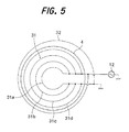
- a fourth embodiment will be described based on FIG. 5 .
- a high frequency antenna 31 whichhas nearly the same diameter as the diameter of a ceiling plate 4, is composed of antennas 31a, 31b, 31c and 31d each in the form of a concentric ring.
- a ring-shaped second antenna 32 is disposed outside of the high frequency antenna 31, namely, outwardly of the ceiling surface.
- a high frequency power source 12 is connected in parallel to the antennas 31a, 31b, 31c, 31d, and the second antenna 32 is connected to the high frequency power source 12 in a state of connection opposite to that for the ring antenna 31. That is, the second antenna 32 is connected to the high frequency power source 12 in a state opposite to the state of connection of the antenna 31 to the high frequency power source 12, namely, such that the connected side and the grounded side for the second antenna 32 are opposite to those for the antenna 31.
- the antenna 31 has nearly the same diameter as the diameter of the ceiling surface.
- a uniform plasma can be generated over a wide range relative to the size of the container 2, there is no decrease in the efficiency, and the uniformity of the plasma within the container 2 can be maintained.
- the plasma CVD apparatus is constituted such that even when a uniform plasma is generated over a wide range within the container 2, the magnetic flux density in the direction of the wall surface can be rendered low, overheating can be avoided, and the occurrence of particles by an etching action can be prevented.
- the present invention is a plasma film deposition apparatus in which a source gas (a material gas: e.g., SiH 4 ) is supplied into a film deposition chamber, and a plasma is generated to excite and activate atoms and molecules, which form a film of silicon oxide or silicon nitride on the surface of a substrate.
- a source gas a material gas: e.g., SiH 4
- a plasma is generated to excite and activate atoms and molecules, which form a film of silicon oxide or silicon nitride on the surface of a substrate.
- power is supplied from above the top of a ceiling surface to a ring-shaped antenna to generate a plasma within a tubular container under an inductively coupled system, thereby forming a film of silicon oxide or silicon nitride on the surface of the substrate.
- the substrate is located in a region where the plasma has a low electron temperature even when the plasma has a high density.
- the region where the plasma is at a high density has an electron density such that there are 1,010 electrons or more per cm 3 .
- the region where the plasma is at a low electron temperature is a region where the electron temperature is 1 electronvolt or less.
- a high frequency power source of 10 MHz to 30 MHz is connected to an antenna, and the distance from the lower surface of the antenna to a substrate is set at 190 mm or more in order to locate the substrate in a region where the electron temperature is 1 electronvolt or less.
- a high frequency power source of 10 MHz to 30 MHz is connected to an antenna, and the distance from the lower surface of the antenna to a substrate is set at 200 mm or more.
- the substrate is located in a region where the electron temperature is low even though the electron density is high. Since the region has a low electron temperature, device destruction due to the charging effect can be suppressed.
- a plasma processing apparatus in which a plasma is generated to excite and activate atoms and molecules, which apply processing, such as etching or ashing, to the surface of a substrate.
- plasma film deposition apparatus plasma CVD apparatus
- a plasma CVD apparatus 81 is furnished with a tubular container (container) 82 of a cylindrical shape and made of aluminum, and a film deposition chamber 3 (for example, diameter 250 mm to 500 mm) is formed within the container 82.
- a circular ceiling plate 84 made of an insulator material (for example, alumina: Al 2 O 3 , thickness 30 mm) is provided at the top of the container 82, and a wafer support base 85 is provided in the film deposition chamber 83 at the center of the container 82.
- the wafer support base 85 has a disk-sh aped bearing portion 87 for holding a semiconductor substrate 86, and the substrate 86 is held on the bearing portion 7, for example, by electrostatic chuck means 88.
- a high frequency antenna 91 as an antenna, for example, in the form of a circular coil ring (flat ring), is placed on the ceiling plate 84, and a high frequency power source 92 (alternating current power source) is connected (high frequency source) to the high frequency antenna 91 via a matching instrument (not shown). Electric power is supplied to the high frequency antenna 91, whereby an electromagnetic wave is thrown into the film deposition chamber 83 of the container 82. The electromagnetic wave, thrown into the container 82, ionizes a gas within the film deposition chamber 83 to generate a plasma.
- a high frequency power source 92 alternating current power source
- the high frequency source with an output of 2 kW to 15 kW (e.g., 5 kW) and a frequency of 10 MHz to 30 MHz (e.g., 13.56 MHz) is connected to the high frequency antenna 91.
- the container 82 is provided with, for example, gas supply nozzles 13 for supplying a material gas, such as silane (for example, SiH 4 ).
- a source gas which serves as a material for film deposition (for example, SiO 2 ), is supplied through the gas supply nozzles 13 into the film deposition chamber 3.
- the container 2 is also provided with auxiliary gas supply nozzles (not shown), which are made of an insulator material (for example, alumina: Al 2 O 3 ), for supplying an inert gas (rare gas) such as argon or helium, or an auxiliary gas such as oxygen or hydrogen.
- the interior of the container 82 is maintained at a predetermined pressure (for example, a vacuum atmosphere on the order of 0.1 Pa to 10 Pa) by a vacuum device 94.
- the container 82 is provided with a carry-in/carry-out port for the substrate 86, although the carry-in/carry-out port is not shown. Through this carry-in/carry-out port, the substrate 86 is carried from a transport chamber (not shown) into the container 82, and carried out of the container 82 to the transport chamber.
- the substrate 86 is placed on the bearing portion 87 of the wafer support base 85, and held (by, for example, electrostatic chuck means 88).
- a predetermined flow rate of the source gas is supplied through the gas supply nozzles 93 into the film deposition chamber 83, and also a predetermined flow rate of the auxiliary gas is supplied through the auxiliary gas supply nozzles into the film deposition chamber 83, with the interior of the film deposition chamber 83 being set at a predetermined pressure suitable for the conditions for film deposition.
- electric power is supplied from the high frequency power source 92 to the high frequency antenna 91 to generate a high frequency electromagnetic wave.
- the material gas within the film deposition chamber 83 is electrically discharged to be partly turned into the state of a plasma.
- This plasma impinges on other neutral molecules in the material gas to ionize or excite the neutral molecules further.
- the thus produced active particles are adsorbed onto the surface of the substrate 86 to cause a chemical reaction with good efficiency, whereby they are deposited.
- the substrate 86 held on the bearing portion 87 of the wafer support base 85 is located in a region where the plasma has a low electron temperature even though the plasma has a high density. That is, the position of the substrate 86 (the height of the bearing portion 87) is set such that the distance H from the lower surface of the high frequency antenna 91 to the substrate 86 is 190 mm to 250 mm (preferably of the order of 200 mm). To adjust the position of the substrate 86, the bearing portion 87 may be rendered free to ascend and descend.
- a high density plasma region is produced which has an electron density of 1,010 electrons or more per cm 3 and has an electron temperature of 1 electronvolt (eV) or less.
- the electron temperature is several eV when the distance H is in a range of 0 mm to less than 190 mm.
- the electron temperature is 1 eV.
- the electron temperature is 1 eV or less.
- the distance H from the lower surface of the high frequency antenna 91 to the substrate 6 should desirably be set at 190 mm to 250 mm.
- a high density plasma region having an electron density of 1,010 electrons or more per cm 3 becomes a region having an electron temperature of 1 electronvolt (eV) or less.
- the substrate 6 is located in the region at a low electron temperature despite a high electron density. Since this region has a low electron temperature, device destruction of the substrate 6 due to the charging effect canbe suppressed.
- a plasma film deposition method in which power is supplied from above a ceiling surface of a tubular container to generate a plasma within the tubular container, and a film is prepared on the surface of a substrate by atoms and molecules excited and activated there.
- the film is produced, with an electric current in a direction opposite to the direction of a feed current for plasma generation being generated outwardly of the ceiling surface.
- a plasma processing method in which power is supplied from above a ceiling surface of a tubular container to generate a plasma within the tubular container, and processing is applied to the surface of a substrate by atoms and molecules excited and activated there.
- processing is applied to the substrate in a region where the plasma has a low electron temperature even though the plasma has a high density.
- the substrate can be located in the region at a low electron temperature despite a high electron density.
- device destruction of the substrate by a charging effect can be suppressed, since the region is at a low electron temperature.
Landscapes
- Chemical & Material Sciences (AREA)
- Engineering & Computer Science (AREA)
- Physics & Mathematics (AREA)
- Plasma & Fusion (AREA)
- Materials Engineering (AREA)
- Chemical Kinetics & Catalysis (AREA)
- General Chemical & Material Sciences (AREA)
- Mechanical Engineering (AREA)
- Metallurgy (AREA)
- Organic Chemistry (AREA)
- Analytical Chemistry (AREA)
- Chemical Vapour Deposition (AREA)
- Plasma Technology (AREA)
- Formation Of Insulating Films (AREA)
- Physical Or Chemical Processes And Apparatus (AREA)
Applications Claiming Priority (3)
| Application Number | Priority Date | Filing Date | Title |
|---|---|---|---|
| JP2002178129A JP3820188B2 (ja) | 2002-06-19 | 2002-06-19 | プラズマ処理装置及びプラズマ処理方法 |
| JP2002351250A JP4052454B2 (ja) | 2002-06-19 | 2002-12-03 | 酸化シリコン膜又は窒化シリコン膜の製造方法 |
| EP03760870A EP1515362B1 (fr) | 2002-06-19 | 2003-06-17 | Systeme de traitement au plasma, procede de traitement au plasma, systeme de depot de film au plasma et procede de depot de film au plasma |
Related Parent Applications (1)
| Application Number | Title | Priority Date | Filing Date |
|---|---|---|---|
| EP03760870.0 Division | 2003-06-17 |
Publications (2)
| Publication Number | Publication Date |
|---|---|
| EP2224468A1 true EP2224468A1 (fr) | 2010-09-01 |
| EP2224468B1 EP2224468B1 (fr) | 2013-08-14 |
Family
ID=30002232
Family Applications (2)
| Application Number | Title | Priority Date | Filing Date |
|---|---|---|---|
| EP10166701.2A Expired - Fee Related EP2224468B1 (fr) | 2002-06-19 | 2003-06-17 | Appareil de traitement plasma, procédé de traitement plasma |
| EP03760870A Expired - Fee Related EP1515362B1 (fr) | 2002-06-19 | 2003-06-17 | Systeme de traitement au plasma, procede de traitement au plasma, systeme de depot de film au plasma et procede de depot de film au plasma |
Family Applications After (1)
| Application Number | Title | Priority Date | Filing Date |
|---|---|---|---|
| EP03760870A Expired - Fee Related EP1515362B1 (fr) | 2002-06-19 | 2003-06-17 | Systeme de traitement au plasma, procede de traitement au plasma, systeme de depot de film au plasma et procede de depot de film au plasma |
Country Status (6)
| Country | Link |
|---|---|
| US (2) | US20050202183A1 (fr) |
| EP (2) | EP2224468B1 (fr) |
| JP (2) | JP3820188B2 (fr) |
| KR (3) | KR100820615B1 (fr) |
| TW (2) | TWI276163B (fr) |
| WO (1) | WO2004001822A1 (fr) |
Families Citing this family (15)
| Publication number | Priority date | Publication date | Assignee | Title |
|---|---|---|---|---|
| TWI408734B (zh) * | 2005-04-28 | 2013-09-11 | Semiconductor Energy Lab | 半導體裝置及其製造方法 |
| JP5162108B2 (ja) * | 2005-10-28 | 2013-03-13 | 日新電機株式会社 | プラズマ生成方法及び装置並びにプラズマ処理装置 |
| US8895388B2 (en) * | 2006-07-21 | 2014-11-25 | Semiconductor Energy Laboratory Co., Ltd. | Method of manufacturing a semiconductor device and a non-volatile semiconductor storage device including the formation of an insulating layer using a plasma treatment |
| KR100808862B1 (ko) * | 2006-07-24 | 2008-03-03 | 삼성전자주식회사 | 기판처리장치 |
| US7972471B2 (en) * | 2007-06-29 | 2011-07-05 | Lam Research Corporation | Inductively coupled dual zone processing chamber with single planar antenna |
| JP5330747B2 (ja) | 2008-06-30 | 2013-10-30 | 三菱重工業株式会社 | 半導体装置用絶縁膜、半導体装置用絶縁膜の製造方法及び製造装置、半導体装置及びその製造方法 |
| JP5723130B2 (ja) * | 2010-09-28 | 2015-05-27 | 東京エレクトロン株式会社 | プラズマ処理装置 |
| JP5800532B2 (ja) * | 2011-03-03 | 2015-10-28 | 東京エレクトロン株式会社 | プラズマ処理装置及びプラズマ処理方法 |
| US10541183B2 (en) | 2012-07-19 | 2020-01-21 | Texas Instruments Incorporated | Spectral reflectometry window heater |
| JP6232953B2 (ja) * | 2013-11-11 | 2017-11-22 | 富士通セミコンダクター株式会社 | 半導体装置の製造装置および半導体装置の製造方法 |
| KR101965992B1 (ko) * | 2014-12-25 | 2019-04-04 | 가부시키가이샤 코쿠사이 엘렉트릭 | 반도체 장치의 제조 방법, 기록 매체 및 기판 처리 장치 |
| CN205741208U (zh) * | 2015-09-16 | 2016-11-30 | 应用材料公司 | 用于改进的等离子体处理腔室的系统和设备 |
| US10544505B2 (en) | 2017-03-24 | 2020-01-28 | Applied Materials, Inc. | Deposition or treatment of diamond-like carbon in a plasma reactor |
| US20180277340A1 (en) * | 2017-03-24 | 2018-09-27 | Yang Yang | Plasma reactor with electron beam of secondary electrons |
| KR101914902B1 (ko) * | 2018-02-14 | 2019-01-14 | 성균관대학교산학협력단 | 플라즈마 발생장치 및 이를 포함하는 기판 처리 장치 |
Citations (6)
| Publication number | Priority date | Publication date | Assignee | Title |
|---|---|---|---|---|
| EP0489407A2 (fr) * | 1990-12-03 | 1992-06-10 | Applied Materials, Inc. | Réacteur à plasma utilisant une source résonante alimentée en UHF/VHF par une antenne et procédé |
| WO1999050883A1 (fr) * | 1998-03-27 | 1999-10-07 | Applied Materials, Inc. | Procede et appareil permettant d'ameliorer le traitement et de reduire les deteriorations provoquees par la charge dans un reacteur a plasma a couplage inductif |
| US6022460A (en) * | 1999-01-18 | 2000-02-08 | Inha University Foundation | Enhanced inductively coupled plasma reactor |
| JP3172340B2 (ja) | 1993-08-12 | 2001-06-04 | 東京エレクトロン株式会社 | プラズマ処理装置 |
| EP1168415A2 (fr) * | 2000-06-23 | 2002-01-02 | Mitsubishi Heavy Industries, Ltd. | Antenne et procédé d'alimentation électrique |
| US20020007794A1 (en) * | 2000-06-01 | 2002-01-24 | Hong-Sik Byun | Plasma processing apparatus |
Family Cites Families (37)
| Publication number | Priority date | Publication date | Assignee | Title |
|---|---|---|---|---|
| US4948458A (en) | 1989-08-14 | 1990-08-14 | Lam Research Corporation | Method and apparatus for producing magnetically-coupled planar plasma |
| JP3005006B2 (ja) | 1989-09-29 | 2000-01-31 | 三菱製紙株式会社 | インクジェット記録媒体 |
| US6165311A (en) * | 1991-06-27 | 2000-12-26 | Applied Materials, Inc. | Inductively coupled RF plasma reactor having an overhead solenoidal antenna |
| JP3249193B2 (ja) | 1992-09-09 | 2002-01-21 | 株式会社ダイヘン | プラズマ処理装置 |
| KR100238627B1 (ko) * | 1993-01-12 | 2000-01-15 | 히가시 데쓰로 | 플라즈마 처리장치 |
| JP3172757B2 (ja) | 1993-05-01 | 2001-06-04 | 東京エレクトロン株式会社 | プラズマ処理装置 |
| US5824158A (en) | 1993-06-30 | 1998-10-20 | Kabushiki Kaisha Kobe Seiko Sho | Chemical vapor deposition using inductively coupled plasma and system therefor |
| KR100276736B1 (ko) * | 1993-10-20 | 2001-03-02 | 히가시 데쓰로 | 플라즈마 처리장치 |
| JPH07201813A (ja) | 1993-12-28 | 1995-08-04 | Fujitsu Ltd | 半導体装置の製造方法およびその製造装置 |
| JPH07245195A (ja) * | 1994-03-07 | 1995-09-19 | Matsushita Electric Ind Co Ltd | プラズマ処理方法及び装置 |
| JP3140934B2 (ja) * | 1994-08-23 | 2001-03-05 | 東京エレクトロン株式会社 | プラズマ装置 |
| JPH08279493A (ja) * | 1995-04-04 | 1996-10-22 | Anelva Corp | プラズマ処理装置 |
| JP3192352B2 (ja) | 1995-06-16 | 2001-07-23 | 東京エレクトロン株式会社 | プラズマ処理装置 |
| US5874704A (en) | 1995-06-30 | 1999-02-23 | Lam Research Corporation | Low inductance large area coil for an inductively coupled plasma source |
| US5907221A (en) * | 1995-08-16 | 1999-05-25 | Applied Materials, Inc. | Inductively coupled plasma reactor with an inductive coil antenna having independent loops |
| US5716451A (en) * | 1995-08-17 | 1998-02-10 | Tokyo Electron Limited | Plasma processing apparatus |
| JP2937907B2 (ja) * | 1995-11-28 | 1999-08-23 | 日本電気株式会社 | プラズマ発生装置 |
| US5936352A (en) * | 1995-11-28 | 1999-08-10 | Nec Corporation | Plasma processing apparatus for producing plasma at low electron temperatures |
| JP3501910B2 (ja) | 1996-04-23 | 2004-03-02 | 東京エレクトロン株式会社 | プラズマ処理装置 |
| EP0805475B1 (fr) | 1996-05-02 | 2003-02-19 | Tokyo Electron Limited | Appareil de traitement par plasma |
| US6170428B1 (en) | 1996-07-15 | 2001-01-09 | Applied Materials, Inc. | Symmetric tunable inductively coupled HDP-CVD reactor |
| US5897712A (en) | 1996-07-16 | 1999-04-27 | Applied Materials, Inc. | Plasma uniformity control for an inductive plasma source |
| TW376547B (en) * | 1997-03-27 | 1999-12-11 | Matsushita Electric Ind Co Ltd | Method and apparatus for plasma processing |
| JP3736016B2 (ja) | 1997-03-27 | 2006-01-18 | 松下電器産業株式会社 | プラズマ処理方法及び装置 |
| JP3726477B2 (ja) * | 1998-03-16 | 2005-12-14 | 株式会社日立製作所 | プラズマ処理装置及びプラズマ処理方法 |
| US6164241A (en) * | 1998-06-30 | 2000-12-26 | Lam Research Corporation | Multiple coil antenna for inductively-coupled plasma generation systems |
| JP2000068254A (ja) * | 1998-08-25 | 2000-03-03 | Matsushita Electronics Industry Corp | プラズマ処理方法とプラズマ処理装置 |
| JP3764594B2 (ja) | 1998-10-12 | 2006-04-12 | 株式会社日立製作所 | プラズマ処理方法 |
| TW469534B (en) | 1999-02-23 | 2001-12-21 | Matsushita Electric Ind Co Ltd | Plasma processing method and apparatus |
| KR100338057B1 (ko) * | 1999-08-26 | 2002-05-24 | 황 철 주 | 유도 결합형 플라즈마 발생용 안테나 장치 |
| JP2001284340A (ja) * | 2000-03-30 | 2001-10-12 | Hitachi Kokusai Electric Inc | 半導体製造装置および半導体装置の製造方法 |
| US6401652B1 (en) * | 2000-05-04 | 2002-06-11 | Applied Materials, Inc. | Plasma reactor inductive coil antenna with flat surface facing the plasma |
| KR100797423B1 (ko) * | 2000-05-17 | 2008-01-23 | 가부시키가이샤 아이에이치아이 | 플라즈마 cvd 장치 및 방법 |
| EP1301938A2 (fr) * | 2000-07-06 | 2003-04-16 | Applied Materials, Inc. | Reacteur a plasma a antenne a enroulements de conducteurs paralleles et symetriques |
| JP2002110565A (ja) | 2000-10-02 | 2002-04-12 | Sony Corp | プラズマ処理装置及び処理方法、並びに半導体装置の製造方法 |
| US6721655B1 (en) | 2001-03-14 | 2004-04-13 | Mitsubishi Denki Kabushiki Kaisha | Vehicle travel guide device and vehicle travel guide method |
| US6660659B1 (en) * | 2002-06-12 | 2003-12-09 | Applied Materials, Inc. | Plasma method and apparatus for processing a substrate |
-
2002
- 2002-06-19 JP JP2002178129A patent/JP3820188B2/ja not_active Expired - Fee Related
- 2002-12-03 JP JP2002351250A patent/JP4052454B2/ja not_active Expired - Fee Related
-
2003
- 2003-06-17 US US10/514,017 patent/US20050202183A1/en not_active Abandoned
- 2003-06-17 KR KR1020077026433A patent/KR100820615B1/ko not_active IP Right Cessation
- 2003-06-17 KR KR1020067012843A patent/KR100806550B1/ko not_active IP Right Cessation
- 2003-06-17 EP EP10166701.2A patent/EP2224468B1/fr not_active Expired - Fee Related
- 2003-06-17 EP EP03760870A patent/EP1515362B1/fr not_active Expired - Fee Related
- 2003-06-17 KR KR1020047020686A patent/KR100661781B1/ko not_active IP Right Cessation
- 2003-06-17 WO PCT/JP2003/007650 patent/WO2004001822A1/fr active Application Filing
- 2003-06-18 TW TW092116541A patent/TWI276163B/zh not_active IP Right Cessation
- 2003-06-18 TW TW095110611A patent/TW200625417A/zh not_active IP Right Cessation
-
2007
- 2007-05-04 US US11/797,601 patent/US8662010B2/en not_active Expired - Fee Related
Patent Citations (6)
| Publication number | Priority date | Publication date | Assignee | Title |
|---|---|---|---|---|
| EP0489407A2 (fr) * | 1990-12-03 | 1992-06-10 | Applied Materials, Inc. | Réacteur à plasma utilisant une source résonante alimentée en UHF/VHF par une antenne et procédé |
| JP3172340B2 (ja) | 1993-08-12 | 2001-06-04 | 東京エレクトロン株式会社 | プラズマ処理装置 |
| WO1999050883A1 (fr) * | 1998-03-27 | 1999-10-07 | Applied Materials, Inc. | Procede et appareil permettant d'ameliorer le traitement et de reduire les deteriorations provoquees par la charge dans un reacteur a plasma a couplage inductif |
| US6022460A (en) * | 1999-01-18 | 2000-02-08 | Inha University Foundation | Enhanced inductively coupled plasma reactor |
| US20020007794A1 (en) * | 2000-06-01 | 2002-01-24 | Hong-Sik Byun | Plasma processing apparatus |
| EP1168415A2 (fr) * | 2000-06-23 | 2002-01-02 | Mitsubishi Heavy Industries, Ltd. | Antenne et procédé d'alimentation électrique |
Non-Patent Citations (1)
| Title |
|---|
| SUMIYA SHIGEAKI ET AL: "Plasma diagnostics and low-temperature deposition of microcrystalline silicon films in ultrahigh-frequency silane plasma", JOURNAL OF APPLIED PHYSICS, AMERICAN INSTITUTE OF PHYSICS. NEW YORK, US LNKD- DOI:10.1063/1.373698, vol. 88, no. 1, 1 July 2000 (2000-07-01), pages 576 - 581, XP012050839, ISSN: 0021-8979 * |
Also Published As
| Publication number | Publication date |
|---|---|
| TW200415710A (en) | 2004-08-16 |
| JP2004022935A (ja) | 2004-01-22 |
| TWI276163B (en) | 2007-03-11 |
| TW200625417A (en) | 2006-07-16 |
| JP4052454B2 (ja) | 2008-02-27 |
| KR20060084067A (ko) | 2006-07-21 |
| TWI305375B (fr) | 2009-01-11 |
| JP3820188B2 (ja) | 2006-09-13 |
| EP1515362B1 (fr) | 2012-07-04 |
| EP1515362A4 (fr) | 2009-07-15 |
| US20070224364A1 (en) | 2007-09-27 |
| KR100806550B1 (ko) | 2008-02-27 |
| WO2004001822A1 (fr) | 2003-12-31 |
| KR20070116184A (ko) | 2007-12-06 |
| JP2004186402A (ja) | 2004-07-02 |
| KR100820615B1 (ko) | 2008-04-08 |
| KR20050012818A (ko) | 2005-02-02 |
| KR100661781B1 (ko) | 2006-12-28 |
| EP2224468B1 (fr) | 2013-08-14 |
| EP1515362A1 (fr) | 2005-03-16 |
| US20050202183A1 (en) | 2005-09-15 |
| US8662010B2 (en) | 2014-03-04 |
Similar Documents
| Publication | Publication Date | Title |
|---|---|---|
| US8662010B2 (en) | Plasma processing apparatus, plasma processing method, plasma film deposition apparatus, and plasma film deposition method | |
| US6422172B1 (en) | Plasma processing apparatus and plasma processing method | |
| KR20050006080A (ko) | 멀티슬롯 안테나를 이용한 표면파 플라즈마 처리장치 | |
| EP0670666A1 (fr) | Appareil de production de plasma et appareil de traitement par plasma | |
| JP2003243378A (ja) | 解離及びイオン化の空間的制御のためのプラズマ処理装置 | |
| JP2001035839A (ja) | プラズマ生成装置および半導体製造方法 | |
| JP2008027816A (ja) | プラズマ処理装置及びプラズマ処理方法 | |
| TWI259037B (en) | Neutral particle beam processing apparatus | |
| US20030010453A1 (en) | Plasma processing apparatus and plasma processing method | |
| WO2012049943A1 (fr) | Dispositif et procédé de formation de film de nitrure de silicium | |
| WO2000032839A1 (fr) | Mode, procede et systeme ameliores au plasma d'implantation ionique par immersion dans le plasma | |
| TW201101414A (en) | Substrate support having side gas outlets and methods | |
| JP3790410B2 (ja) | パーティクル低減方法 | |
| EP3719833B1 (fr) | Appareil de traitement de surface | |
| JP3955351B2 (ja) | プラズマ処理装置 | |
| KR100899768B1 (ko) | 플라즈마 기판 처리 장치 | |
| JP3082659B2 (ja) | プラズマ処理装置 | |
| TWI797833B (zh) | 用於使用電容耦合電漿的氧化矽間隙填充的沉積方法 | |
| JPH1022279A (ja) | 誘導結合型プラズマcvd装置 | |
| JP2001342567A (ja) | プラズマ処理装置 | |
| JP3683044B2 (ja) | 静電チャック板とその製造方法 | |
| JP2006140534A (ja) | 給電アンテナ及びこれを有する半導体製造装置 | |
| JPH11251092A (ja) | 反応性イオンエッチング装置 | |
| JP2000345352A (ja) | プラズマ成膜処理方法 |
Legal Events
| Date | Code | Title | Description |
|---|---|---|---|
| PUAI | Public reference made under article 153(3) epc to a published international application that has entered the european phase |
Free format text: ORIGINAL CODE: 0009012 |
|
| 17P | Request for examination filed |
Effective date: 20100621 |
|
| AC | Divisional application: reference to earlier application |
Ref document number: 1515362 Country of ref document: EP Kind code of ref document: P |
|
| AK | Designated contracting states |
Kind code of ref document: A1 Designated state(s): DE FR GB |
|
| RTI1 | Title (correction) |
Free format text: PLASMA PROCESSING APPARATUS, PLASMA PROCESSING METHOD |
|
| 17Q | First examination report despatched |
Effective date: 20111207 |
|
| REG | Reference to a national code |
Ref country code: DE Ref legal event code: R079 Ref document number: 60344765 Country of ref document: DE Free format text: PREVIOUS MAIN CLASS: H01L0021205000 Ipc: H01J0037320000 |
|
| RIC1 | Information provided on ipc code assigned before grant |
Ipc: H01J 37/32 20060101AFI20121128BHEP Ipc: C23C 16/507 20060101ALI20121128BHEP |
|
| GRAP | Despatch of communication of intention to grant a patent |
Free format text: ORIGINAL CODE: EPIDOSNIGR1 |
|
| GRAS | Grant fee paid |
Free format text: ORIGINAL CODE: EPIDOSNIGR3 |
|
| GRAA | (expected) grant |
Free format text: ORIGINAL CODE: 0009210 |
|
| AC | Divisional application: reference to earlier application |
Ref document number: 1515362 Country of ref document: EP Kind code of ref document: P |
|
| AK | Designated contracting states |
Kind code of ref document: B1 Designated state(s): DE FR GB |
|
| REG | Reference to a national code |
Ref country code: GB Ref legal event code: FG4D |
|
| REG | Reference to a national code |
Ref country code: DE Ref legal event code: R096 Ref document number: 60344765 Country of ref document: DE Effective date: 20131010 |
|
| PLBE | No opposition filed within time limit |
Free format text: ORIGINAL CODE: 0009261 |
|
| STAA | Information on the status of an ep patent application or granted ep patent |
Free format text: STATUS: NO OPPOSITION FILED WITHIN TIME LIMIT |
|
| 26N | No opposition filed |
Effective date: 20140515 |
|
| REG | Reference to a national code |
Ref country code: DE Ref legal event code: R097 Ref document number: 60344765 Country of ref document: DE Effective date: 20140515 |
|
| GBPC | Gb: european patent ceased through non-payment of renewal fee |
Effective date: 20140617 |
|
| PG25 | Lapsed in a contracting state [announced via postgrant information from national office to epo] |
Ref country code: GB Free format text: LAPSE BECAUSE OF NON-PAYMENT OF DUE FEES Effective date: 20140617 |
|
| REG | Reference to a national code |
Ref country code: FR Ref legal event code: PLFP Year of fee payment: 14 |
|
| REG | Reference to a national code |
Ref country code: FR Ref legal event code: PLFP Year of fee payment: 15 |
|
| PGFP | Annual fee paid to national office [announced via postgrant information from national office to epo] |
Ref country code: FR Payment date: 20170511 Year of fee payment: 15 Ref country code: DE Payment date: 20170613 Year of fee payment: 15 |
|
| REG | Reference to a national code |
Ref country code: DE Ref legal event code: R119 Ref document number: 60344765 Country of ref document: DE |
|
| PG25 | Lapsed in a contracting state [announced via postgrant information from national office to epo] |
Ref country code: FR Free format text: LAPSE BECAUSE OF NON-PAYMENT OF DUE FEES Effective date: 20180630 Ref country code: DE Free format text: LAPSE BECAUSE OF NON-PAYMENT OF DUE FEES Effective date: 20190101 |