EP2215719B1 - Angepasste integrierte elektronische komponenten - Google Patents
Angepasste integrierte elektronische komponenten Download PDFInfo
- Publication number
- EP2215719B1 EP2215719B1 EP08843885.8A EP08843885A EP2215719B1 EP 2215719 B1 EP2215719 B1 EP 2215719B1 EP 08843885 A EP08843885 A EP 08843885A EP 2215719 B1 EP2215719 B1 EP 2215719B1
- Authority
- EP
- European Patent Office
- Prior art keywords
- elements
- port
- integrated electronic
- coupled
- amplifier
- Prior art date
- Legal status (The legal status is an assumption and is not a legal conclusion. Google has not performed a legal analysis and makes no representation as to the accuracy of the status listed.)
- Active
Links
- 230000008878 coupling Effects 0.000 claims description 11
- 238000010168 coupling process Methods 0.000 claims description 11
- 238000005859 coupling reaction Methods 0.000 claims description 11
- 238000000034 method Methods 0.000 claims description 7
- 239000004065 semiconductor Substances 0.000 claims description 7
- 230000001939 inductive effect Effects 0.000 claims description 4
- 238000004519 manufacturing process Methods 0.000 claims description 3
- 238000010586 diagram Methods 0.000 description 9
- 239000003990 capacitor Substances 0.000 description 5
- 238000013461 design Methods 0.000 description 4
- 230000002250 progressing effect Effects 0.000 description 3
- 238000003491 array Methods 0.000 description 2
- 230000014509 gene expression Effects 0.000 description 2
- 238000000638 solvent extraction Methods 0.000 description 2
- 230000001413 cellular effect Effects 0.000 description 1
- 238000012512 characterization method Methods 0.000 description 1
- 238000011161 development Methods 0.000 description 1
- 230000000694 effects Effects 0.000 description 1
- 238000005516 engineering process Methods 0.000 description 1
- 230000002708 enhancing effect Effects 0.000 description 1
- 238000003384 imaging method Methods 0.000 description 1
- 230000010354 integration Effects 0.000 description 1
- 229910021420 polycrystalline silicon Inorganic materials 0.000 description 1
- 229920005591 polysilicon Polymers 0.000 description 1
- 238000012545 processing Methods 0.000 description 1
Images


Classifications
-
- H—ELECTRICITY
- H03—ELECTRONIC CIRCUITRY
- H03H—IMPEDANCE NETWORKS, e.g. RESONANT CIRCUITS; RESONATORS
- H03H7/00—Multiple-port networks comprising only passive electrical elements as network components
- H03H7/24—Frequency- independent attenuators
-
- H—ELECTRICITY
- H01—ELECTRIC ELEMENTS
- H01L—SEMICONDUCTOR DEVICES NOT COVERED BY CLASS H10
- H01L27/00—Devices consisting of a plurality of semiconductor or other solid-state components formed in or on a common substrate
- H01L27/02—Devices consisting of a plurality of semiconductor or other solid-state components formed in or on a common substrate including semiconductor components specially adapted for rectifying, oscillating, amplifying or switching and having potential barriers; including integrated passive circuit elements having potential barriers
- H01L27/0203—Particular design considerations for integrated circuits
- H01L27/0207—Geometrical layout of the components, e.g. computer aided design; custom LSI, semi-custom LSI, standard cell technique
-
- H—ELECTRICITY
- H03—ELECTRONIC CIRCUITRY
- H03F—AMPLIFIERS
- H03F3/00—Amplifiers with only discharge tubes or only semiconductor devices as amplifying elements
- H03F3/45—Differential amplifiers
- H03F3/45071—Differential amplifiers with semiconductor devices only
- H03F3/45076—Differential amplifiers with semiconductor devices only characterised by the way of implementation of the active amplifying circuit in the differential amplifier
- H03F3/45475—Differential amplifiers with semiconductor devices only characterised by the way of implementation of the active amplifying circuit in the differential amplifier using IC blocks as the active amplifying circuit
-
- H—ELECTRICITY
- H03—ELECTRONIC CIRCUITRY
- H03G—CONTROL OF AMPLIFICATION
- H03G1/00—Details of arrangements for controlling amplification
- H03G1/0005—Circuits characterised by the type of controlling devices operated by a controlling current or voltage signal
- H03G1/0088—Circuits characterised by the type of controlling devices operated by a controlling current or voltage signal using discontinuously variable devices, e.g. switch-operated
-
- H—ELECTRICITY
- H03—ELECTRONIC CIRCUITRY
- H03H—IMPEDANCE NETWORKS, e.g. RESONANT CIRCUITS; RESONATORS
- H03H7/00—Multiple-port networks comprising only passive electrical elements as network components
- H03H7/38—Impedance-matching networks
-
- H—ELECTRICITY
- H03—ELECTRONIC CIRCUITRY
- H03F—AMPLIFIERS
- H03F2203/00—Indexing scheme relating to amplifiers with only discharge tubes or only semiconductor devices as amplifying elements covered by H03F3/00
- H03F2203/45—Indexing scheme relating to differential amplifiers
- H03F2203/45048—Calibrating and standardising a dif amp
-
- H—ELECTRICITY
- H03—ELECTRONIC CIRCUITRY
- H03F—AMPLIFIERS
- H03F2203/00—Indexing scheme relating to amplifiers with only discharge tubes or only semiconductor devices as amplifying elements covered by H03F3/00
- H03F2203/45—Indexing scheme relating to differential amplifiers
- H03F2203/45136—One differential amplifier in IC-block form being shown
-
- H—ELECTRICITY
- H03—ELECTRONIC CIRCUITRY
- H03F—AMPLIFIERS
- H03F2203/00—Indexing scheme relating to amplifiers with only discharge tubes or only semiconductor devices as amplifying elements covered by H03F3/00
- H03F2203/45—Indexing scheme relating to differential amplifiers
- H03F2203/45522—Indexing scheme relating to differential amplifiers the FBC comprising one or more potentiometers
-
- H—ELECTRICITY
- H03—ELECTRONIC CIRCUITRY
- H03F—AMPLIFIERS
- H03F2203/00—Indexing scheme relating to amplifiers with only discharge tubes or only semiconductor devices as amplifying elements covered by H03F3/00
- H03F2203/45—Indexing scheme relating to differential amplifiers
- H03F2203/45528—Indexing scheme relating to differential amplifiers the FBC comprising one or more passive resistors and being coupled between the LC and the IC
-
- H—ELECTRICITY
- H03—ELECTRONIC CIRCUITRY
- H03F—AMPLIFIERS
- H03F2203/00—Indexing scheme relating to amplifiers with only discharge tubes or only semiconductor devices as amplifying elements covered by H03F3/00
- H03F2203/45—Indexing scheme relating to differential amplifiers
- H03F2203/45534—Indexing scheme relating to differential amplifiers the FBC comprising multiple switches and being coupled between the LC and the IC
-
- H—ELECTRICITY
- H03—ELECTRONIC CIRCUITRY
- H03F—AMPLIFIERS
- H03F2203/00—Indexing scheme relating to amplifiers with only discharge tubes or only semiconductor devices as amplifying elements covered by H03F3/00
- H03F2203/45—Indexing scheme relating to differential amplifiers
- H03F2203/45591—Indexing scheme relating to differential amplifiers the IC comprising one or more potentiometers
-
- H—ELECTRICITY
- H03—ELECTRONIC CIRCUITRY
- H03F—AMPLIFIERS
- H03F2203/00—Indexing scheme relating to amplifiers with only discharge tubes or only semiconductor devices as amplifying elements covered by H03F3/00
- H03F2203/45—Indexing scheme relating to differential amplifiers
- H03F2203/45594—Indexing scheme relating to differential amplifiers the IC comprising one or more resistors, which are not biasing resistor
-
- H—ELECTRICITY
- H03—ELECTRONIC CIRCUITRY
- H03F—AMPLIFIERS
- H03F2203/00—Indexing scheme relating to amplifiers with only discharge tubes or only semiconductor devices as amplifying elements covered by H03F3/00
- H03F2203/45—Indexing scheme relating to differential amplifiers
- H03F2203/45616—Indexing scheme relating to differential amplifiers the IC comprising more than one switch, which are not cross coupled
-
- Y—GENERAL TAGGING OF NEW TECHNOLOGICAL DEVELOPMENTS; GENERAL TAGGING OF CROSS-SECTIONAL TECHNOLOGIES SPANNING OVER SEVERAL SECTIONS OF THE IPC; TECHNICAL SUBJECTS COVERED BY FORMER USPC CROSS-REFERENCE ART COLLECTIONS [XRACs] AND DIGESTS
- Y10—TECHNICAL SUBJECTS COVERED BY FORMER USPC
- Y10T—TECHNICAL SUBJECTS COVERED BY FORMER US CLASSIFICATION
- Y10T29/00—Metal working
- Y10T29/49—Method of mechanical manufacture
- Y10T29/49002—Electrical device making
- Y10T29/4902—Electromagnet, transformer or inductor
-
- Y—GENERAL TAGGING OF NEW TECHNOLOGICAL DEVELOPMENTS; GENERAL TAGGING OF CROSS-SECTIONAL TECHNOLOGIES SPANNING OVER SEVERAL SECTIONS OF THE IPC; TECHNICAL SUBJECTS COVERED BY FORMER USPC CROSS-REFERENCE ART COLLECTIONS [XRACs] AND DIGESTS
- Y10—TECHNICAL SUBJECTS COVERED BY FORMER USPC
- Y10T—TECHNICAL SUBJECTS COVERED BY FORMER US CLASSIFICATION
- Y10T29/00—Metal working
- Y10T29/49—Method of mechanical manufacture
- Y10T29/49002—Electrical device making
- Y10T29/49082—Resistor making
-
- Y—GENERAL TAGGING OF NEW TECHNOLOGICAL DEVELOPMENTS; GENERAL TAGGING OF CROSS-SECTIONAL TECHNOLOGIES SPANNING OVER SEVERAL SECTIONS OF THE IPC; TECHNICAL SUBJECTS COVERED BY FORMER USPC CROSS-REFERENCE ART COLLECTIONS [XRACs] AND DIGESTS
- Y10—TECHNICAL SUBJECTS COVERED BY FORMER USPC
- Y10T—TECHNICAL SUBJECTS COVERED BY FORMER US CLASSIFICATION
- Y10T29/00—Metal working
- Y10T29/49—Method of mechanical manufacture
- Y10T29/49002—Electrical device making
- Y10T29/49105—Switch making
Definitions
- the invention relates to a switchable integrated electronic device, to electronic circuits comprising the switchable integrated electronic device, and to method of manufacturing a switchable integrated electronic device, and in particular addresses the layout of such devices and circuits.
- Resistor layout differs somewhat from that of transistor layout. Straight-line resistors are usually avoided and each resistor is implemented by a series/parallel combination of a number of unit resistors. The most popular layout technique is interleaving.
- US 4,280,089 discloses an attenuation arrangement comprising a step attenuator arranged in cascade with a controllable voltage divider via first and second voltage terminals.
- the step attenuator comprises a series arrangement of attenuation elements for dividing a voltage applied across the series arrangement into a plurality of voltage increments.
- the voltage increments are individually switchable between the two voltage terminals for varying the output voltage of the controllable voltage divider.
- a switchable integrated electronic device comprising:
- a method of manufacturing a switchable integrated electronic device comprising:
- the invention provides a layout for successive series coupled elements of a switchable electronic device that enables components comprising the elements to be well matched irrespective of the switch setting, by ensuring a good interleaving of the elements of the components.
- the elements are resistors that determine the gain of an amplifier
- the resistance between the first port and the third port, and between the second port and the third port can be well matched regardless of gain setting of the amplifier, and hence the ratio of these resistances has a low spread.
- the invention is applicable to components with either large or small ratios.
- the N elements all comprise one of a resistive element, a capacitive element, an inductive element, and a semiconductor element.
- all of the elements are of the same type, e.g. resistive element, capacitive element, inductive element, semiconductor element etc.
- the invention is applicable to a chain of series coupled resistors, a chain of series coupled capacitors, a chain of series coupled inductors, or a chain of series coupled semiconductor devices etc.
- the invention also provides an electronic circuit, comprising a first switchable integrated electronic device according to the first aspect of the invention having its first port coupled to a first circuit input and its second port coupled to a circuit output, wherein the N elements of the first switchable integrated electronic device each comprise a resistive element, and wherein the electronic circuit further comprises an amplifier having a first amplifier input coupled to the third port of the first switchable integrated electronic device and an amplifier output coupled to the circuit output.
- the invention provides a switchable-gain amplifier having its gain determined by switchable resistors which are well matched regardless of the selected gain. Hence the gain has a low spread in value.
- the invention also provides an electronic circuit as stated above and further comprising a second switchable integrated electronic device according to the first aspect of the invention having its first port coupled to a second circuit input, its second port coupled to ground or a voltage source, and its third port coupled to a second amplifier input of the amplifier, wherein the first and second amplifier inputs are respectively inverting and non-inverting, and wherein the N elements of the second switchable integrated electronic device each comprise a resistive element.
- the invention provides a switchable-gain amplifier having inverting and non-inverting inputs and which has its gain determined by switchable resistors which are well matched regardless of the gain setting selected.
- the first and second switchable integrated electronic devices may comprise an equal number of the N elements and the respective switch means of the first and second switchable integrated electronic devices may be adapted to couple a corresponding selectable one of the nodes of the first and second switchable integrated electronic devices to the respective third ports. This feature enables the inverting and non-inverting inputs to remain well balanced regardless of which gain setting is selected.
- an audio amplifier 100 capable of driving a load such as an earphone, in a difference amplifier configuration having inverting and non-inverting inputs, 22 and 24. It comprises an operational amplifier 10 having an inverting input 12 and a non-inverting input 14, and an output 16. There is a resistance R1 coupled between a first input 22 of the audio amplifier 100 and the inverting input 12, and a resistance R2 coupled between the inverting input 12 and the output 16. There is a resistance R3 coupled between a second input 24 of the audio amplifier 100 and the non-inverting input 14, and a resistance R4 coupled between the non-inverting input 14 and a ground point GND indicated by reference numeral 18. Instead of being coupled to ground, the resistance R4 may alternatively be coupled to a voltage source or another point in the amplifier 100 circuit.
- FIG 3 illustrates in more detail the audio amplifier 100 of Figure 2 , in particular illustrating how the components R1, R2, R3 and R4 are formed.
- the combination R1, R2 is formed as a chain of series coupled resistors r 1 ...r 14 .
- There is a switch bank 30 comprising switches a1...a13 for coupling a selectable one of the nodes between any two successive resistors in the chain of resistors r 1 ...r 14 to the inverting input 12.
- the combination R3, R4 is formed as a chain of series coupled resistors s 1 ...s 14 .
- Correspondingly numbered resistors r 1 ...r 14 and s 1 ...s 14 have nominally equal resistance values, although this is not essential to the invention.
- switch bank 50 comprising switches b1...b13 for coupling a selectable one of the nodes between any two adjacent resistors in the chain of resistors s 1 ...s 14 to the non-inverting input 14.
- the closure of the switches a1...a13 and b1...b13 is made under the control of a decoder 40, with correspondingly numbered switches a1...a13 and b1...b13 being operated together.
- the values of R1 and R2 are selected by partitioning the resistors r 1 ,..r 14 by closing a selected one of the switches a1...a13
- the values of R3 and R4 are selected by partitioning the resistors s 1 ...s 14 by closing a selected one of the switches b1...b13.
- switches a11 and b11 are illustrated in the closed position with the other switches all open.
- R1 comprises r 1 , r 2 and r 3
- R2 comprises r 4 ...r 14
- R3 comprises s 1 , s 2 , and s 3
- R4 comprises s 4 ...s 14
- the decoder 40 has thirteen output lines 44 for controlling the thirteen switch pairs a1/b1, a2/b2,...a13/b13, and four input lines 42 for a binary signal indicating which of the thirteen switch pairs are to be closed.
- Vout 1 + R ⁇ 2 R ⁇ 1 ⁇ R ⁇ 4 R ⁇ 3 + R ⁇ 4 ⁇ Vip - R ⁇ 2 R ⁇ 1 ⁇ Vin
- Vin is the voltage at the inverting input 22
- Vip is the voltage at the non-inverting input 24.
- the configuration illustrated in Figure 3 requires 2*(N+1) resistors and 2N switches.
- the resistances R1 and R2 can be expressed as R ⁇ 1 ⁇
- R1 and R3 decrease, and R2 and R4 increase, by the same amount, corresponding to the gain step size.
- the gain error depends on the achievable degree of matching of ratio the ratios R2/R1 and R4/R3. Because the resistances of R1 to R4 vary as the gain is switched, the constellation of R1 and R2 changes, even though the resistors r 1 ...r 14 and s 1 ...s 13 all have fixed positions.
- interleaving must be maintained for best matching at each gain setting, as will now be described. Only the layout for R1 and R2 will be described, as the layout for R3 and R4 can follow the same principles.
- resistors r 1 ...r 14 and their interconnection is illustrated in Figure 4 . From left to right, the order of placement of the resistors is r 7 , r 9 , r 5 , r 11 , r 3 , r 13 , r 1 , r 14 , r 2 , r 12 , r 4 , r 10 , r 6 , and r 8 . All resistors are connected, as indicated in Figure 3 , in series, thus forming a resistor chain. The switches a1...
- FIG. 6 shows a layout of the components R1, R2, R3, R4, the switch bank 30 and the decoder 40 in 65nm CMOS.
- each resistor r 1 ...r 14 is implemented with a four-line array of unit resistors of polysilicon type, and about half dummy resistors have been added to occupy otherwise vacant space in the layout and to ensure the end resistors r 7 and r 8 have neighbours on both sides for best matching.
- the switch bank 30 and the decoder 40 have been placed between the resistor arrays to provide an equai distance to the resistor arrays.
- a single input amplifier having a non-balanced input, may be formed simply by grounding the non-inverting input 14 of the amplifier illustrated in Figure 2 , thereby avoiding the requirement for the combination R3, R4.
- the interleaving arrangement can be extended to any number of gain settings and generalised.
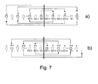
- a generalised embodiment will be described with reference to Figure 7 in which the boxes each represent a resistive element, the numbers above the boxes represent the order of the element in the series forming the chain, and the numbers below the boxes represent the positions of the elements in the layout.
- the arrangement will be described in two stages, considering first the positions of the elements indicated by solid lines in diagram a) of Figure 7 , and secondly the positions of the elements indicated by solid lines diagram b) in Figure 7 .
- N be the total number of resistor elements connected in series, in order from r 1 to r N . If N is even, we first divide the elements into two subsets. The first N/2 elements form one subset and the rest form the other. All N elements will be placed in a row of size N. The positions for the elements are numbered from 1 to N, from left to right. Starting with the first subset of elements which are indicated by the solid lines in diagram a), first we position element r 1 at position N/2, then the elements r 2 and r 3 at positions respectively second right and second left, to element 1, i.e., at positions N/2+2 and N/2-2, respectively. Then elements r 4 , r 5 , r 6 , ...
- r N/2 are positioned one after another at every alternate position on alternating sides of element r 1 in the same fashion.
- the arrow lines above and below the elements in diagram a) of Figure 7 indicate the coupling between successive elements in the chain, and are illustrated progressing in a clock wise direction.
- element r N at position N/2+1, then element r N-1 , r N-2 ,...r N/2+1 , at every alternate position to the last element placed. This time the coupling between successive elements in the chain progresses anti-clockwise. If N/2 is odd, the most left element will be r N/2 , and if N/2 is even, element r N/2 will be at the far right.
- N is odd, we can first disregard element r (N+1)/2 and position the even number of elements N-1 as described above, and finally, place element (N+1)/2 at either the left-most or right-most position.
- the order may instead be alternately left and right of the initial element.
- the elements of the second subset will progress alternately right and left, because the first element of the second subset is always on the opposite side to the last element of the first subset.
- Either end of the chain may be considered to be the first port, with the other end being the second port.
- the position of the elements may be expressed mathematically in the following generalised forms, for N elements r 1 ...r N series coupled in numerical order, where adjacent positions are numbered consecutively.
- Element r i has position ⁇ N + 1 2 ⁇ + - 1 i .2.
- ⁇ i 2 ⁇ for i 1 to ⁇ N 2 ⁇ and position ⁇ N + 1 2 ⁇ + - 1 i . 2.
- ⁇ N - i 2 ⁇ + 1 for i ⁇ N 2 ⁇ + 1 to N.
- the invention is equally applicable to the layout of capacitors, inductors or semiconductor components such as transistors, which may therefore be coupled in a corresponding series arrangement and laid out in a corresponding interleaved arrangement.
- each element has been described as a single entity, each element may comprise a series or parallel arrangement of sub-elements having the same or different resistance, capacitance or inductance, thereby enabling components having any desired value to be formed from sub-elements.
- some dummy sub-elements may be included in the layout that do not contribute to the in-circuit resistance, capacitance or inductance, but merely serve to enable a symmetrical layout for best matching and to occupy vacant area.
Landscapes
- Engineering & Computer Science (AREA)
- Power Engineering (AREA)
- General Engineering & Computer Science (AREA)
- Physics & Mathematics (AREA)
- Condensed Matter Physics & Semiconductors (AREA)
- General Physics & Mathematics (AREA)
- Computer Hardware Design (AREA)
- Microelectronics & Electronic Packaging (AREA)
- Semiconductor Integrated Circuits (AREA)
- Design And Manufacture Of Integrated Circuits (AREA)
- Control Of Amplification And Gain Control (AREA)
Claims (7)
- Schaltbare integrierte elektronische Vorrichtung, die Folgendes umfasst:N Elemente (r1...r14; s1...s14), wobei N eine Ganzzahl größer zwei ist, eine Serie, die in einer Kette zwischen einem ersten Anschluss und einem zweiten Anschluss gekoppelt ist, wobei Knoten zwischen aufeinanderfolgenden Elementen (r1...r14; s1...s14) der Kette angeordnet sind; undSchaltmittel (30; 50) zum Koppeln eines wählbaren Knotens mit einem dritten Anschluss;dadurch gekennzeichnet, dass eine Anordnung der Elemente das i-te der aufeinanderfolgenden Elemente (R1...R14; s1...s14) der Kette umfasst, die in einer k-ten aufeinanderfolgenden Position einer Reihe angeordnet ist, wobei i=1 bis N, wobei


- Schaltbare integrierte elektronische Vorrichtung nach Anspruch 1, wobei die N Elemente (r1...r14; s1...s14) alle ein Widerstandselement, ein kapazitives Element, ein induktives Element oder ein Halbleiterelement umfassen.
- Elektronische Schaltung (100), die eine erste schaltbare integrierte elektronische Vorrichtung nach Anspruch 1 umfasst, deren erster Anschluss mit einem ersten Schaltungseingang (22) gekoppelt ist und deren zweiter Anschluss mit einem Schaltungsausgang gekoppelt ist, wobei die N Elemente (r1...r14; s1...s14) der ersten schaltbaren integrierten elektronischen Vorrichtung jeweils ein Widerstandselement umfassen und wobei die elektronische Schaltung (100) ferner einen Verstärker (10) umfasst, der Folgendes aufweist: einen ersten Verstärkereingang (12), der mit dem dritten Anschluss der ersten schaltbaren integrierten elektronischen Vorrichtung gekoppelt ist, und einen Verstärkerausgang (16), der mit dem Schaltungsausgang gekoppelt ist.
- Elektronische Schaltung (100) nach Anspruch 3, die eine zweite schaltbare integrierte elektronische Vorrichtung nach Anspruch 1 umfasst, wobei: ihr erster Anschluss mit einem zweiten Schaltungseingang (24) gekoppelt ist, ihr zweiter Anschluss mit Masse (18) oder einer Spannungsquelle gekoppelt ist und ihr dritter Anschluss mit einem zweiten Verstärkereingang (14) des Verstärkers (10) gekoppelt ist, wobei der erste und zweite Verstärkereingang (12, 14) jeweils invertierend und nichtinvertierend ist und wobei die N Elemente (r1...r14; s1...s14) der zweiten schaltbaren integrierten elektronischen Vorrichtung jeweils ein Widerstandselement umfassen.
- Elektronische Schaltung (100) nach Anspruch 4, wobei die erste und zweite schaltbare integrierte elektronische Vorrichtung eine gleiche Anzahl der N Elemente (r1...r14; s1...s14) umfasst und wobei die jeweiligen Schaltmittel (30; 50) der ersten und zweiten schaltbaren integrierten elektronischen Vorrichtung dafür ausgelegt sind, einen entsprechenden auswählbaren der Knoten der ersten und zweiten schaltbaren integrierten elektronischen Vorrichtung mit dem jeweiligen dritten Anschluss zu koppeln.
- Verfahren zur Herstellung einer schaltbaren integrierten elektronischen Vorrichtung, das Folgendes umfasst:Bilden von N Elementen (r1...r14; s1...s14), wobei N eine Ganzzahl größer zwei ist, einer Serie, die zwischen einem ersten Anschluss und einem zweiten Anschluss in einer Kette gekoppelt ist und Knoten zwischen aufeinanderfolgenden Elementen (r1... r14; s1...s14) der Kette bereitstellt;Bilden von Schaltmitteln (30; 50) zum Koppeln eines wählbaren Knotens mit einem dritten Anschluss;dadurch gekennzeichnet, dass eine Anordnung der Elemente (r1...r14; s1...s14) das i-te der aufeinanderfolgenden Elemente (r1...r14; s1...s14) der Kette umfasst, die in einer k-ten aufeinanderfolgenden Position einer Reihe angeordnet ist, wobei i = 1 bis N ist, wobei


- Verfahren nach Anspruch 6, das das Bilden jedes der Elemente (r1...r14; s1...s14) als Widerstandselement, kapazitives Element, induktives Element oder Halbleiterelement umfasst.
Priority Applications (1)
| Application Number | Priority Date | Filing Date | Title |
|---|---|---|---|
| EP08843885.8A EP2215719B1 (de) | 2007-11-02 | 2008-10-31 | Angepasste integrierte elektronische komponenten |
Applications Claiming Priority (3)
| Application Number | Priority Date | Filing Date | Title |
|---|---|---|---|
| EP07119900 | 2007-11-02 | ||
| EP08843885.8A EP2215719B1 (de) | 2007-11-02 | 2008-10-31 | Angepasste integrierte elektronische komponenten |
| PCT/EP2008/009354 WO2009056360A1 (en) | 2007-11-02 | 2008-10-31 | Matched integrated electronic components |
Publications (2)
| Publication Number | Publication Date |
|---|---|
| EP2215719A1 EP2215719A1 (de) | 2010-08-11 |
| EP2215719B1 true EP2215719B1 (de) | 2015-10-21 |
Family
ID=40262255
Family Applications (1)
| Application Number | Title | Priority Date | Filing Date |
|---|---|---|---|
| EP08843885.8A Active EP2215719B1 (de) | 2007-11-02 | 2008-10-31 | Angepasste integrierte elektronische komponenten |
Country Status (5)
| Country | Link |
|---|---|
| US (1) | US8344822B2 (de) |
| EP (1) | EP2215719B1 (de) |
| JP (1) | JP5296798B2 (de) |
| CN (1) | CN101983479B (de) |
| WO (1) | WO2009056360A1 (de) |
Families Citing this family (3)
| Publication number | Priority date | Publication date | Assignee | Title |
|---|---|---|---|---|
| WO2014187503A1 (en) * | 2013-05-24 | 2014-11-27 | Pierburg Pump Technology Gmbh | Variable displacement lubricant pump |
| US9065400B2 (en) | 2013-09-20 | 2015-06-23 | Honeywell International Inc. | Programmable-gain instrumentation amplifier |
| US10644675B2 (en) * | 2017-10-02 | 2020-05-05 | Robert Bosch Gmbh | Switched resistance device with reduced sensitivity to parasitic capacitance |
Family Cites Families (9)
| Publication number | Priority date | Publication date | Assignee | Title |
|---|---|---|---|---|
| NL7811229A (nl) * | 1978-11-14 | 1980-05-19 | Philips Nv | Verzwakkerinrichting bevattende een cascadeschakeling van een stappenverzwakker en een regelbare spannings- deler, alsmede een besturingsschakeling voor de rege- ling daarvan. |
| JPS58198922A (ja) * | 1982-05-17 | 1983-11-19 | Hitachi Ltd | 半導体集積回路によるd/a変換回路 |
| JPS5929447A (ja) | 1982-08-12 | 1984-02-16 | Nec Corp | 半導体集積回路装置 |
| DE59107736D1 (de) * | 1991-08-24 | 1996-05-30 | Itt Ind Gmbh Deutsche | Monolithisch integrierter Differenzverstärker mit digitaler Verstärkungseinstellung |
| US6060760A (en) | 1997-08-13 | 2000-05-09 | Tritech Microelectronics, Ltd. | Optimal resistor network layout |
| JP2000294732A (ja) * | 1999-04-02 | 2000-10-20 | Fuji Electric Co Ltd | 半導体装置 |
| US6617989B2 (en) | 2001-12-21 | 2003-09-09 | Texas Instruments Incorporated | Resistor string DAC with current source LSBs |
| JP4103849B2 (ja) * | 2003-05-28 | 2008-06-18 | ヤマハ株式会社 | D/aコンバータ |
| WO2007102133A1 (en) * | 2006-03-09 | 2007-09-13 | Nxp B.V. | Radio receiver |
-
2008
- 2008-10-31 WO PCT/EP2008/009354 patent/WO2009056360A1/en active Application Filing
- 2008-10-31 JP JP2010532490A patent/JP5296798B2/ja not_active Expired - Fee Related
- 2008-10-31 CN CN200880123464.4A patent/CN101983479B/zh active Active
- 2008-10-31 EP EP08843885.8A patent/EP2215719B1/de active Active
-
2010
- 2010-04-30 US US12/771,718 patent/US8344822B2/en active Active
Also Published As
| Publication number | Publication date |
|---|---|
| EP2215719A1 (de) | 2010-08-11 |
| US8344822B2 (en) | 2013-01-01 |
| JP2011503856A (ja) | 2011-01-27 |
| CN101983479A (zh) | 2011-03-02 |
| CN101983479B (zh) | 2014-07-16 |
| WO2009056360A1 (en) | 2009-05-07 |
| US20100271126A1 (en) | 2010-10-28 |
| JP5296798B2 (ja) | 2013-09-25 |
Similar Documents
| Publication | Publication Date | Title |
|---|---|---|
| KR101866103B1 (ko) | 스위칭가능한 캐패시턴스를 위한 시스템 및 방법 | |
| US7453136B2 (en) | Methods, systems, and apparatus for integrated circuit capacitors in capacitor arrays | |
| EP2337219A1 (de) | Digitaler Abschwächer mit geringer Phasenvariation | |
| US6636821B2 (en) | Output driver impedance calibration circuit | |
| EP2522073A1 (de) | Analoge breitband-funkfrequenz-komponenten | |
| EP2215719B1 (de) | Angepasste integrierte elektronische komponenten | |
| JP2006211021A (ja) | フィルタ回路 | |
| USRE45634E1 (en) | Multiple-input and multiple-output amplifier using mutual induction in the feedback network | |
| US6344780B1 (en) | Impedance adjusting circuit | |
| US6507272B1 (en) | Enhanced linearity, low switching perturbation resistor string matrices | |
| US8115575B2 (en) | Active inductor for ASIC application | |
| CN111106832A (zh) | Dac版图结构和电阻分压式dac | |
| WO2015040756A1 (ja) | スイッチ付容量及びスイッチ付容量を含む回路 | |
| US7177895B2 (en) | Linear channel select filter | |
| Henrici et al. | A field programmable analog array using floating gates for high resolution tuning | |
| JPH1155059A (ja) | 可変減衰器 | |
| US8963629B2 (en) | Variable admittance circuit | |
| EP1523093B1 (de) | Frequenzkompensation eines Breitbandoperationsverstärkers | |
| US20210083661A1 (en) | Variable capacitance circuit | |
| Kumar et al. | A systematic realization of current mode universal biquad filters | |
| Wang et al. | Versatile multi-function universal voltage-mode filter |
Legal Events
| Date | Code | Title | Description |
|---|---|---|---|
| PUAI | Public reference made under article 153(3) epc to a published international application that has entered the european phase |
Free format text: ORIGINAL CODE: 0009012 |
|
| 17P | Request for examination filed |
Effective date: 20100601 |
|
| AK | Designated contracting states |
Kind code of ref document: A1 Designated state(s): AT BE BG CH CY CZ DE DK EE ES FI FR GB GR HR HU IE IS IT LI LT LU LV MC MT NL NO PL PT RO SE SI SK TR |
|
| AX | Request for extension of the european patent |
Extension state: AL BA MK RS |
|
| RAP1 | Party data changed (applicant data changed or rights of an application transferred) |
Owner name: ST-ERICSSON SA |
|
| 17Q | First examination report despatched |
Effective date: 20101015 |
|
| DAX | Request for extension of the european patent (deleted) | ||
| GRAP | Despatch of communication of intention to grant a patent |
Free format text: ORIGINAL CODE: EPIDOSNIGR1 |
|
| INTG | Intention to grant announced |
Effective date: 20150605 |
|
| GRAS | Grant fee paid |
Free format text: ORIGINAL CODE: EPIDOSNIGR3 |
|
| GRAA | (expected) grant |
Free format text: ORIGINAL CODE: 0009210 |
|
| AK | Designated contracting states |
Kind code of ref document: B1 Designated state(s): AT BE BG CH CY CZ DE DK EE ES FI FR GB GR HR HU IE IS IT LI LT LU LV MC MT NL NO PL PT RO SE SI SK TR |
|
| REG | Reference to a national code |
Ref country code: GB Ref legal event code: FG4D Ref country code: NL Ref legal event code: MP Effective date: 20151021 |
|
| REG | Reference to a national code |
Ref country code: CH Ref legal event code: EP |
|
| REG | Reference to a national code |
Ref country code: AT Ref legal event code: REF Ref document number: 757171 Country of ref document: AT Kind code of ref document: T Effective date: 20151115 |
|
| REG | Reference to a national code |
Ref country code: IE Ref legal event code: FG4D |
|
| REG | Reference to a national code |
Ref country code: DE Ref legal event code: R096 Ref document number: 602008040818 Country of ref document: DE |
|
| REG | Reference to a national code |
Ref country code: FR Ref legal event code: PLFP Year of fee payment: 8 |
|
| REG | Reference to a national code |
Ref country code: LT Ref legal event code: MG4D |
|
| REG | Reference to a national code |
Ref country code: AT Ref legal event code: MK05 Ref document number: 757171 Country of ref document: AT Kind code of ref document: T Effective date: 20151021 |
|
| PG25 | Lapsed in a contracting state [announced via postgrant information from national office to epo] |
Ref country code: LT Free format text: LAPSE BECAUSE OF FAILURE TO SUBMIT A TRANSLATION OF THE DESCRIPTION OR TO PAY THE FEE WITHIN THE PRESCRIBED TIME-LIMIT Effective date: 20151021 Ref country code: NL Free format text: LAPSE BECAUSE OF FAILURE TO SUBMIT A TRANSLATION OF THE DESCRIPTION OR TO PAY THE FEE WITHIN THE PRESCRIBED TIME-LIMIT Effective date: 20151021 Ref country code: IT Free format text: LAPSE BECAUSE OF FAILURE TO SUBMIT A TRANSLATION OF THE DESCRIPTION OR TO PAY THE FEE WITHIN THE PRESCRIBED TIME-LIMIT Effective date: 20151021 Ref country code: IS Free format text: LAPSE BECAUSE OF FAILURE TO SUBMIT A TRANSLATION OF THE DESCRIPTION OR TO PAY THE FEE WITHIN THE PRESCRIBED TIME-LIMIT Effective date: 20160221 Ref country code: NO Free format text: LAPSE BECAUSE OF FAILURE TO SUBMIT A TRANSLATION OF THE DESCRIPTION OR TO PAY THE FEE WITHIN THE PRESCRIBED TIME-LIMIT Effective date: 20160121 Ref country code: HR Free format text: LAPSE BECAUSE OF FAILURE TO SUBMIT A TRANSLATION OF THE DESCRIPTION OR TO PAY THE FEE WITHIN THE PRESCRIBED TIME-LIMIT Effective date: 20151021 Ref country code: ES Free format text: LAPSE BECAUSE OF FAILURE TO SUBMIT A TRANSLATION OF THE DESCRIPTION OR TO PAY THE FEE WITHIN THE PRESCRIBED TIME-LIMIT Effective date: 20151021 |
|
| PG25 | Lapsed in a contracting state [announced via postgrant information from national office to epo] |
Ref country code: PL Free format text: LAPSE BECAUSE OF FAILURE TO SUBMIT A TRANSLATION OF THE DESCRIPTION OR TO PAY THE FEE WITHIN THE PRESCRIBED TIME-LIMIT Effective date: 20151021 Ref country code: FI Free format text: LAPSE BECAUSE OF FAILURE TO SUBMIT A TRANSLATION OF THE DESCRIPTION OR TO PAY THE FEE WITHIN THE PRESCRIBED TIME-LIMIT Effective date: 20151021 Ref country code: GR Free format text: LAPSE BECAUSE OF FAILURE TO SUBMIT A TRANSLATION OF THE DESCRIPTION OR TO PAY THE FEE WITHIN THE PRESCRIBED TIME-LIMIT Effective date: 20160122 Ref country code: LV Free format text: LAPSE BECAUSE OF FAILURE TO SUBMIT A TRANSLATION OF THE DESCRIPTION OR TO PAY THE FEE WITHIN THE PRESCRIBED TIME-LIMIT Effective date: 20151021 Ref country code: SE Free format text: LAPSE BECAUSE OF FAILURE TO SUBMIT A TRANSLATION OF THE DESCRIPTION OR TO PAY THE FEE WITHIN THE PRESCRIBED TIME-LIMIT Effective date: 20151021 Ref country code: AT Free format text: LAPSE BECAUSE OF FAILURE TO SUBMIT A TRANSLATION OF THE DESCRIPTION OR TO PAY THE FEE WITHIN THE PRESCRIBED TIME-LIMIT Effective date: 20151021 Ref country code: PT Free format text: LAPSE BECAUSE OF FAILURE TO SUBMIT A TRANSLATION OF THE DESCRIPTION OR TO PAY THE FEE WITHIN THE PRESCRIBED TIME-LIMIT Effective date: 20160222 |
|
| REG | Reference to a national code |
Ref country code: CH Ref legal event code: PL |
|
| REG | Reference to a national code |
Ref country code: DE Ref legal event code: R097 Ref document number: 602008040818 Country of ref document: DE |
|
| REG | Reference to a national code |
Ref country code: IE Ref legal event code: MM4A |
|
| PG25 | Lapsed in a contracting state [announced via postgrant information from national office to epo] |
Ref country code: LI Free format text: LAPSE BECAUSE OF NON-PAYMENT OF DUE FEES Effective date: 20151031 Ref country code: CZ Free format text: LAPSE BECAUSE OF FAILURE TO SUBMIT A TRANSLATION OF THE DESCRIPTION OR TO PAY THE FEE WITHIN THE PRESCRIBED TIME-LIMIT Effective date: 20151021 Ref country code: MC Free format text: LAPSE BECAUSE OF FAILURE TO SUBMIT A TRANSLATION OF THE DESCRIPTION OR TO PAY THE FEE WITHIN THE PRESCRIBED TIME-LIMIT Effective date: 20151021 Ref country code: CH Free format text: LAPSE BECAUSE OF NON-PAYMENT OF DUE FEES Effective date: 20151031 |
|
| PLBE | No opposition filed within time limit |
Free format text: ORIGINAL CODE: 0009261 |
|
| STAA | Information on the status of an ep patent application or granted ep patent |
Free format text: STATUS: NO OPPOSITION FILED WITHIN TIME LIMIT |
|
| PG25 | Lapsed in a contracting state [announced via postgrant information from national office to epo] |
Ref country code: EE Free format text: LAPSE BECAUSE OF FAILURE TO SUBMIT A TRANSLATION OF THE DESCRIPTION OR TO PAY THE FEE WITHIN THE PRESCRIBED TIME-LIMIT Effective date: 20151021 Ref country code: RO Free format text: LAPSE BECAUSE OF FAILURE TO SUBMIT A TRANSLATION OF THE DESCRIPTION OR TO PAY THE FEE WITHIN THE PRESCRIBED TIME-LIMIT Effective date: 20151021 Ref country code: SK Free format text: LAPSE BECAUSE OF FAILURE TO SUBMIT A TRANSLATION OF THE DESCRIPTION OR TO PAY THE FEE WITHIN THE PRESCRIBED TIME-LIMIT Effective date: 20151021 Ref country code: DK Free format text: LAPSE BECAUSE OF FAILURE TO SUBMIT A TRANSLATION OF THE DESCRIPTION OR TO PAY THE FEE WITHIN THE PRESCRIBED TIME-LIMIT Effective date: 20151021 |
|
| REG | Reference to a national code |
Ref country code: FR Ref legal event code: PLFP Year of fee payment: 9 |
|
| 26N | No opposition filed |
Effective date: 20160722 |
|
| PG25 | Lapsed in a contracting state [announced via postgrant information from national office to epo] |
Ref country code: IE Free format text: LAPSE BECAUSE OF NON-PAYMENT OF DUE FEES Effective date: 20151031 |
|
| PG25 | Lapsed in a contracting state [announced via postgrant information from national office to epo] |
Ref country code: SI Free format text: LAPSE BECAUSE OF FAILURE TO SUBMIT A TRANSLATION OF THE DESCRIPTION OR TO PAY THE FEE WITHIN THE PRESCRIBED TIME-LIMIT Effective date: 20151021 |
|
| PG25 | Lapsed in a contracting state [announced via postgrant information from national office to epo] |
Ref country code: BE Free format text: LAPSE BECAUSE OF FAILURE TO SUBMIT A TRANSLATION OF THE DESCRIPTION OR TO PAY THE FEE WITHIN THE PRESCRIBED TIME-LIMIT Effective date: 20151021 |
|
| REG | Reference to a national code |
Ref country code: DE Ref legal event code: R081 Ref document number: 602008040818 Country of ref document: DE Owner name: OCT CIRCUIT TECHNOLOGIES INTERNATIONAL LTD., IE Free format text: FORMER OWNER: ST-ERICSSON SA, PLAN-LES-OUATES, CH |
|
| PG25 | Lapsed in a contracting state [announced via postgrant information from national office to epo] |
Ref country code: BG Free format text: LAPSE BECAUSE OF FAILURE TO SUBMIT A TRANSLATION OF THE DESCRIPTION OR TO PAY THE FEE WITHIN THE PRESCRIBED TIME-LIMIT Effective date: 20151021 Ref country code: HU Free format text: LAPSE BECAUSE OF FAILURE TO SUBMIT A TRANSLATION OF THE DESCRIPTION OR TO PAY THE FEE WITHIN THE PRESCRIBED TIME-LIMIT; INVALID AB INITIO Effective date: 20081031 |
|
| PG25 | Lapsed in a contracting state [announced via postgrant information from national office to epo] |
Ref country code: CY Free format text: LAPSE BECAUSE OF FAILURE TO SUBMIT A TRANSLATION OF THE DESCRIPTION OR TO PAY THE FEE WITHIN THE PRESCRIBED TIME-LIMIT Effective date: 20151021 |
|
| PG25 | Lapsed in a contracting state [announced via postgrant information from national office to epo] |
Ref country code: MT Free format text: LAPSE BECAUSE OF FAILURE TO SUBMIT A TRANSLATION OF THE DESCRIPTION OR TO PAY THE FEE WITHIN THE PRESCRIBED TIME-LIMIT Effective date: 20151021 Ref country code: TR Free format text: LAPSE BECAUSE OF FAILURE TO SUBMIT A TRANSLATION OF THE DESCRIPTION OR TO PAY THE FEE WITHIN THE PRESCRIBED TIME-LIMIT Effective date: 20151021 |
|
| REG | Reference to a national code |
Ref country code: FR Ref legal event code: PLFP Year of fee payment: 10 |
|
| PG25 | Lapsed in a contracting state [announced via postgrant information from national office to epo] |
Ref country code: LU Free format text: LAPSE BECAUSE OF NON-PAYMENT OF DUE FEES Effective date: 20151031 |
|
| REG | Reference to a national code |
Ref country code: FR Ref legal event code: TP Owner name: OCT CIRCUIT TECHNOLOGIES INTERNATIONAL LIMITED, IE Effective date: 20180116 |
|
| REG | Reference to a national code |
Ref country code: FR Ref legal event code: PLFP Year of fee payment: 11 |
|
| REG | Reference to a national code |
Ref country code: GB Ref legal event code: 732E Free format text: REGISTERED BETWEEN 20210722 AND 20210728 |
|
| REG | Reference to a national code |
Ref country code: GB Ref legal event code: 732E Free format text: REGISTERED BETWEEN 20210805 AND 20210811 |
|
| PGFP | Annual fee paid to national office [announced via postgrant information from national office to epo] |
Ref country code: GB Payment date: 20231027 Year of fee payment: 16 |
|
| PGFP | Annual fee paid to national office [announced via postgrant information from national office to epo] |
Ref country code: FR Payment date: 20231025 Year of fee payment: 16 Ref country code: DE Payment date: 20231027 Year of fee payment: 16 |