EP2204469A1 - Magnetroneinheit, magnetron-sputtering-vorrchtung und verfahren zur herstellung einer elektronischen vorrichtung - Google Patents
Magnetroneinheit, magnetron-sputtering-vorrchtung und verfahren zur herstellung einer elektronischen vorrichtung Download PDFInfo
- Publication number
- EP2204469A1 EP2204469A1 EP08843409A EP08843409A EP2204469A1 EP 2204469 A1 EP2204469 A1 EP 2204469A1 EP 08843409 A EP08843409 A EP 08843409A EP 08843409 A EP08843409 A EP 08843409A EP 2204469 A1 EP2204469 A1 EP 2204469A1
- Authority
- EP
- European Patent Office
- Prior art keywords
- magnet
- magnetron unit
- magnetron
- magnet element
- target
- Prior art date
- Legal status (The legal status is an assumption and is not a legal conclusion. Google has not performed a legal analysis and makes no representation as to the accuracy of the status listed.)
- Withdrawn
Links
Images


Classifications
-
- C—CHEMISTRY; METALLURGY
- C23—COATING METALLIC MATERIAL; COATING MATERIAL WITH METALLIC MATERIAL; CHEMICAL SURFACE TREATMENT; DIFFUSION TREATMENT OF METALLIC MATERIAL; COATING BY VACUUM EVAPORATION, BY SPUTTERING, BY ION IMPLANTATION OR BY CHEMICAL VAPOUR DEPOSITION, IN GENERAL; INHIBITING CORROSION OF METALLIC MATERIAL OR INCRUSTATION IN GENERAL
- C23C—COATING METALLIC MATERIAL; COATING MATERIAL WITH METALLIC MATERIAL; SURFACE TREATMENT OF METALLIC MATERIAL BY DIFFUSION INTO THE SURFACE, BY CHEMICAL CONVERSION OR SUBSTITUTION; COATING BY VACUUM EVAPORATION, BY SPUTTERING, BY ION IMPLANTATION OR BY CHEMICAL VAPOUR DEPOSITION, IN GENERAL
- C23C14/00—Coating by vacuum evaporation, by sputtering or by ion implantation of the coating forming material
- C23C14/22—Coating by vacuum evaporation, by sputtering or by ion implantation of the coating forming material characterised by the process of coating
- C23C14/34—Sputtering
- C23C14/35—Sputtering by application of a magnetic field, e.g. magnetron sputtering
-
- C—CHEMISTRY; METALLURGY
- C23—COATING METALLIC MATERIAL; COATING MATERIAL WITH METALLIC MATERIAL; CHEMICAL SURFACE TREATMENT; DIFFUSION TREATMENT OF METALLIC MATERIAL; COATING BY VACUUM EVAPORATION, BY SPUTTERING, BY ION IMPLANTATION OR BY CHEMICAL VAPOUR DEPOSITION, IN GENERAL; INHIBITING CORROSION OF METALLIC MATERIAL OR INCRUSTATION IN GENERAL
- C23C—COATING METALLIC MATERIAL; COATING MATERIAL WITH METALLIC MATERIAL; SURFACE TREATMENT OF METALLIC MATERIAL BY DIFFUSION INTO THE SURFACE, BY CHEMICAL CONVERSION OR SUBSTITUTION; COATING BY VACUUM EVAPORATION, BY SPUTTERING, BY ION IMPLANTATION OR BY CHEMICAL VAPOUR DEPOSITION, IN GENERAL
- C23C14/00—Coating by vacuum evaporation, by sputtering or by ion implantation of the coating forming material
- C23C14/22—Coating by vacuum evaporation, by sputtering or by ion implantation of the coating forming material characterised by the process of coating
- C23C14/56—Apparatus specially adapted for continuous coating; Arrangements for maintaining the vacuum, e.g. vacuum locks
- C23C14/562—Apparatus specially adapted for continuous coating; Arrangements for maintaining the vacuum, e.g. vacuum locks for coating elongated substrates
-
- H—ELECTRICITY
- H01—ELECTRIC ELEMENTS
- H01J—ELECTRIC DISCHARGE TUBES OR DISCHARGE LAMPS
- H01J37/00—Discharge tubes with provision for introducing objects or material to be exposed to the discharge, e.g. for the purpose of examination or processing thereof
- H01J37/32—Gas-filled discharge tubes
- H01J37/34—Gas-filled discharge tubes operating with cathodic sputtering
- H01J37/3402—Gas-filled discharge tubes operating with cathodic sputtering using supplementary magnetic fields
- H01J37/3405—Magnetron sputtering
- H01J37/3408—Planar magnetron sputtering
-
- H—ELECTRICITY
- H01—ELECTRIC ELEMENTS
- H01J—ELECTRIC DISCHARGE TUBES OR DISCHARGE LAMPS
- H01J37/00—Discharge tubes with provision for introducing objects or material to be exposed to the discharge, e.g. for the purpose of examination or processing thereof
- H01J37/32—Gas-filled discharge tubes
- H01J37/34—Gas-filled discharge tubes operating with cathodic sputtering
- H01J37/3411—Constructional aspects of the reactor
- H01J37/345—Magnet arrangements in particular for cathodic sputtering apparatus
- H01J37/3455—Movable magnets
Definitions
- the present invention relates to a magnetron unit for a magnetron sputtering apparatus which deposits films of a material on a substrate such as a wafer and, more particularly, to a magnetron unit for a magnetron type sputtering apparatus, a magnetron sputtering apparatus, and a method of manufacturing an electronic device, which use a scheme (to be referred to as an "in-line scheme" hereinafter) of depositing a film while the wafer, which is facing the sputtering target, is scanned next to the target.
- a scheme to be referred to as an "in-line scheme” hereinafter
- a sputtering apparatus generates a plasma, and causes ions generated by the plasma to collide with a target so as to expel a target material and make it adhere to a substrate, thereby forming a film.
- an apparatus called a magnetron type apparatus generates a magnetic field parallel to a target surface by a cathode magnet (magnetron unit) placed on the rear surface of the target. Since this magnetic field crosses the electric field between the target and the substrate, electrons emitted from the target are confined near the target to increase the plasma density. For this reason, the film formation rate in a magnetron type sputtering apparatus strongly depends on the strength of the electric field and leakage magnetic field formed on the target.
- the strength of a magnetic field from the magnetron unit placed on the rear surface of a target has a significant effect on plasma density and influences the film thickness distribution on a substrate.
- the plasma density increases. This raises the sputtering rate, and hence increases the film formation rate at a particular location on the substrate.
- a target 7 is formed into a rectangular shape extending in a direction perpendicular to the transport direction of a substrate (film formation substrate 9) such as a wafer.
- a magnetron unit 28 on the rear surface side of the target 7 has a structure having a rectangular annular clearance. Permanent magnets having different magnetic poles, which correspond to the entire area of the target 7, are provided in the rectangular annular clearance portion.
- the number of sputter particles from the two sides of the rectangular target (target 7) in the longitudinal direction is small ( Fig. 15 ), and hence the film thicknesses on the two ends of the substrate tend to be less than that on the middle portion ( Fig. 16 ).
- it is necessary to improve the film thickness distribution by making some large-scale changes, for example, increasing the length of the target 7 in the direction (y direction) perpendicular to the transport direction (x direction) of the substrate 9.
- the target 7 and the magnetron unit 28 need to be elongated in a direction perpendicular to the substrate transport direction. For these reasons, there have been demands for a rectangular magnetron unit which allows easy adjustment of a film thickness distribution on outer peripheral portions of a substrate.
- a magnet is configured to increase the magnetic field strength at the two sides of a target in the longitudinal direction.
- the magnet has a continuous shape. For this reason, in order to adjust the magnetic field, the entire magnet needs to be redesigned or replaced.
- a magnetron unit comprising a plurality of first magnet elements each including first magnets which have the same polarity and are provided on two end portions of a yoke plate made of a magnetic material and a second magnet which has a polarity different from that of the first magnets and is provided on a middle portion of the yoke plate, a base plate which is placed to allow the respective first magnet elements to be translated in one direction, and second magnet elements which are respectively fixed on two ends of the base plate in one direction and each include a magnet having the same polarity as that of the first magnet of the first magnet element.
- the present invention it is possible to accurately and easily perform film thickness adjustment without increasing the length of a target and magnetron unit. Achieving the desired film thickness distribution on the entire substrate is therefore easier.
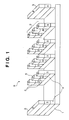
- Fig. 1 shows an example of the arrangement of a magnetron unit 8 of the present invention.
- the magnetron unit 8 in this case includes a rectangular plate 1 and first and second magnet elements 2 and 3 which are arranged parallel to each other on the rectangular plate 1 in the longitudinal direction.
- the first magnet element 2 includes a yoke plate 4 and first and second magnets 5 and 6 having different polarities.
- the yoke plate 4 is made of a magnetic material, and is configured to extend in a direction perpendicular to the longitudinal direction(transverse direction).
- the first magnets 5 having the same polarity are provided on the two ends of the yoke plate 4.
- the second magnet 6 is fixed at the middle portion of the yoke plate 4.
- the first magnet elements 2 are arranged parallel to each other along the longitudinal direction of the rectangular plate 1, and can be moved by a sliding mechanism including a linear guide 15 and rails 13 as shown in, for example, Fig. 5A .
- the transport mechanism can position the first magnet element 2 at an arbitrary position in the longitudinal direction.
- the second magnet elements 3 are fixed on the two ends of the rectangular plate 1 in the transverse direction through the yoke plates 4.
- the second magnet element 3 has a magnet 3a with the same polarity (the S pole in the case shown in Fig. 1 ) as that of the second magnet 6 on the yoke plate 4.
- the second magnet element 3 has a magnet 3b with the same polarity (the N pole in the case shown in Fig. 1 ) as that of the first magnet 5. It is disposed on the magnet 3a with the same polarity as that of the second magnet 6 on the yoke plate 4.
- the magnetron unit 8 having such an arrangement can be placed on the rear surface of the target of a sputtering apparatus based on the in-line scheme.
- the magnetic field strength at an end portion of a target 7 which corresponds to the corresponding place increases ( Fig. 2B ).
- the magnetic field strength at the end portion of the target 7 decreases ( Fig. 2A ).
- the magnetic field strength can be changed and the film thickness distribution on the film formation substrate can be adjusted by linear adjustment of the positions of the first magnet elements 2 along the longitudinal direction of the rectangular plate 1.
- the following is a form of the sputtering apparatus to which the magnetron unit 8 of the present invention can be applied.
- Fig. 3 is a schematic view showing the main part of the sputtering apparatus according to the first embodiment of the present invention.
- the magnetron unit 8 having the arrangement shown in Fig. 1 described above is placed on the rear surface (upper surface side) of the rectangular target 7.
- a substrate 9 such as a wafer is placed on a substrate stage 11 on the opposite side (lower surface side) to the rear surface of the target 7.
- Applying the magnetron unit 8 of the present invention to the sputtering apparatus in this manner can suppress reductions in film thickness on the outer peripheral portions of the substrate.
- a significant portion of deposited particles come from the two ends of the target 7 in the longitudinal direction.
- Fig. 4 is a schematic view showing the main parts of a sputtering apparatus according to the second embodiment of the present invention.
- a magnetron unit 8 having the arrangement shown in Fig. 1 described above is placed on the rear surface (upper surface side) of a rectangular target 7, and a substrate 9 is placed on the opposite side (lower surface side) to the rear surface of the target 7.
- the second embodiment differs from the first embodiment as for the means of scanning the substrate.
- the substrate stage 11 has a shaft 12 parallel to the longitudinal direction of the target 7.
- the substrate stage 11 rotates about the shaft 12 to make the substrate 9 pass through the front surface of the target 7.
- This embodiment can also suppress reductions in film thickness on outer peripheral portions of the film formation substrate which correspond to the two ends of the target 7 in the longitudinal direction.
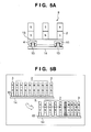
- Fig. 5A is an end view showing an arrangement of the first magnet elements of the magnetron unit 8.
- Fig. 5B is a side view showing an example of how first magnet elements 2 of the magnetron unit 8 are adjusted.
- Fig. 5B aims to show an example of movement/adjustment of the first magnet elements 2.
- the number of first magnet elements 2 shown in Fig. 5B is not meant to be a limitation for the present invention.
- the magnetron unit 8 includes a plurality of first magnet elements 2, rails 13 for the longitudinal movement of the first magnet elements 2, a base plate 14, and second magnet elements 3 fixed to the two ends of the base plate 14.
- the base plate 14 corresponds to the rectangular plate 1 in Fig. 1 .
- the two rails 13 are fixed on one surface of the base plate 14 and parallel to the longitudinal direction.
- Two linear guides 15 are fixed to the lower portions of the yoke plates 4 of each first magnet element 2.
- the central portions of the linear guides 15 and rails 13 have similar widths. Fitting the rails 13 in the linear guides 15 makes it possible for the respective first magnet elements 2 to freely move along the rails 13 on the base plate 14 ( Fig. 5A ).
- the second magnet elements 3 located on the two ends of the magnetron unit 8 in the longitudinal direction are fixed to the base plate 14.
- one of the first magnet elements 2 for example the first magnet element indicated by the hatching in Fig. 5B
- the distances between the magnet elements on either side of the relocated first magnet elements are reduced almost uniformly due to the repulsive forces of the magnetic poles facing each other.
- the distances between the magnets of the magnet element array, which are located on the opposite side in the moving direction prolong due to the repulsive force of the magnetic poles facing each other ( Fig. 5B ).
- the magnetic field strength on the surface of the target 7 including the magnetron unit 8 described above can be adjusted at the two ends of the target 7.
- FIGS. 6A and 6B are schematic views each showing an example of the moving mechanism for an arbitrary first magnet elements 2.
- Figs. 7A and 7B are views for explaining the arrangement of the moving mechanism shown in Figs. 6A and 6B .
- Fig. 7C is a view showing an example of the arrangement of the second magnet element 3.
- first magnet elements 2A are arranged parallel to each other on the middle portion of the base plate 14 as a rectangular plate in the longitudinal direction.
- a plurality of first magnet elements are arranged parallel to each other on the two sides of the array of the two magnet elements 2A in the longitudinal direction of the base plate 14.
- three magnet elements 2B are arranged on the left side of the magnet elements 2A, and three magnet elements 2B are arranged on the right side of the magnet elements 2A.
- the second magnet elements 3 are respectively arranged on the left and right ends of the base plate 14.
- magnet elements 2A and 2B can be freely moved in the longitudinal direction of the base plate 14 by the moving mechanism (guide means) including the rails 13 and the linear guides 15 described above.
- Each magnet element 2A is provided with a screw hole 16 extending through the surfaces of the yoke plate 4 in the moving direction, as shown in Fig. 7A .
- Each magnet element 2B is provided with a through hole 17 extending through the surfaces of the yoke plate 4 in the moving direction, as shown in Fig. 7B .
- the hole diameter of the through hole 17 is designed to be larger than the hole diameter (tap diameter) of the screw hole 16.
- the second magnet element 3 is provided with the through hole 17 in the surfaces of the yoke plate 4 in the moving direction.
- the hole diameter of the through hole 17 is designed to be larger than the hole diameter (tap diameter) of the screw hole 16.
- each screw 18 extends through the through holes 17 of the yoke plates 4 of the second magnet element 3 and the plurality of magnet elements 2B, and is attached to the screw hole 16 of the yoke plate 4 of one magnet element 2A.
- motors 610 and 620 function as driving mechanisms for rotating/driving the screws 18.
- Detection means 630 and 640 which are formed by, for example, encoders, detect the rotational speeds and rotational angles of the motors 610 and 620, respectively.
- a controller 650 determines the travel distance of the magnet elements 2A by controlling the rotational speeds or rotational angles of the motors 610 and 620 based on detection information from the detection means 630 and 640 and the pitch of each screw 18 as a known parameter.
- each screw 18 forcibly moves the magnet element 2A on the rails 13 upon rotation of the screw 18.
- a plurality of magnet elements 2B rearrange themselves along the rails 13 independently of the rotation of the screws 18 ( Fig. 6B ) due to the repulsive force of the adjacent magnet elements.
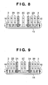
- Figs. 8 and 9 show other examples of the magnet elements 2A and 2B.
- the control system including the motors 610 and 620, the detection means 630 and 640, and the controller 650 will not be illustrated in Figs. 8 and 9.
- Figs. 8 and 9 show an example of the arrangement of the magnet elements 2A and 2B.
- the number of magnet elements 2B is not necessarily limited by that is shown in Figs. 8 and 9 .
- a magnet element 2C including one or two first magnet elements is placed on the middle portion of the base plate 14.
- the two magnet elements 2A are arranged parallel to each other on the two sides of the magnet element 2C in the longitudinal direction.
- a plurality of magnet elements 2B are arranged parallel to each other on the two sides of the array of the magnet elements 2A and 2C in the longitudinal direction of the base plate 14.
- the second magnet elements 3 are fixed to the two ends of the base plate 14.
- the magnet elements 2A, 2B, and 2C correspond to the first magnet elements 2, and can be freely moved along the rails 13 described above in the longitudinal direction of the base plate 14. As the magnet elements 2A are forcibly moved by rotating the screws 18, the plurality of magnet elements 2B move due to the repulsive force of the magnets.
- the magnetic field strength at the two ends of the target can be adjusted to be higher than that on the middle portion. This adjustment causes more sputter particles from the two end portions of the target in the longitudinal direction to be deposited onto the substrate, thereby suppressing abrupt reductions in film thickness on the outer peripheral portions of the substrate.
- the magnet element 2C on the middle portion of the base plate 14 is not forcibly moved by the screws 18 and is left near the middle portion.
- the purpose of this arrangement is to prevent the plasma discharge from becoming unstable due to an abrupt reduction in magnetic field near the middle portion of the target.
- Fig. 8 shows a case in which one magnet element 2C is used.
- Fig. 9 shows a case in which two magnet elements 2C are used.
- the present invention is not limited to these examples. It is possible to arrange two or more magnet elements 2C to avoid abrupt fluctuations in magnetic field in the middle portion of the base plate 14 and stabilize the discharge.
- the number of magnet elements 2C left near the middle portion of the base plate is preferably determined to make 1) the magnetic field strength at the middle portion of the magnetron unit become lower than that at the two ends of the magnetron unit in the longitudinal direction and to make 2) the leakage magnetic field to the middle portion of the magnetron unit to be 300 G or more.
- Fig. 10 is a schematic view of a sputtering apparatus according to the third embodiment.
- the apparatus in Fig. 10 includes a substrate holder 19 which linearly moves in a direction crossing the longitudinal direction of a target 7 (preferably a horizontal direction perpendicular to the longitudinal direction).
- the substrate holder 19 holds a substrate 9 and can be scanned back and forth along a rail 20 below the substrate holder 19.
- the substrate holder 19 and the target 7 placed below a magnetron unit 8 are arranged in a vacuum chamber 21 so as to face each other.
- Magnet elements 2 (not shown in Fig. 10 ) of the magnetron unit 8 are arranged in a direction perpendicular to the moving direction (the direction indicated by the arrow) of the substrate holder 19.
- the vacuum chamber 21 includes a process gas introduction port 22, a vacuum pump 23, and an exhaust port 24.
- the magnetron unit 8 be placed on the rear surface side of the target 7 to swing in the moving direction of the substrate holder 19 by using an oscillating mechanism.
- Fig. 11 is a schematic view of a sputtering apparatus according to the fourth embodiment.
- the apparatus in Fig. 11 includes a substrate holder 19 which pans in a direction crossing the longitudinal direction of a target 7 (a horizontal direction intersecting at a right angle).
- the substrate holder 19 and the target 7 placed in a magnetron unit 8 are arranged in a vacuum chamber 21 so as to face each other.
- magnet elements 2 (not shown in Fig. 11 ) of the magnetron unit 8 are arranged in a direction perpendicular to the moving direction of the substrate holder 19.
- the magnetron unit 8 and the substrate holder 19 respectively have rotating shafts 12 and 25, and can freely rotate about the rotating shafts 12 and 25. Rotating the magnetron unit 8 and the substrate holder 19 about the rotating shafts 12 and 25 in opposite directions can change the offset distance while always maintaining the positional relationship between the target 7 and the substrate holder 19 in a horizontal state. That is, from the viewpoint of the target 7, this state is equivalent to a state in which the substrate holder 19 passes through a space on the cathode surface side.
- the magnetron unit 8 placed on the rear surface side of the target 7 to oscillate in the moving direction of the substrate holder.
- the magnet element 2A is moved by rotating the screw 18, and each magnet element 2B is moved by the repulsive force of a magnetic field (magnetic force) formed by the magnets having the same polarity.
- the repulsive force of a magnetic field is small in the following cases: the magnetic field formed by the magnet elements 2A and 2B is weak, the magnetic field between the adjacent magnet elements 2B is weak, the magnet elements 2A and 2B are spaced far apart from each other, and the adjacent magnet elements 2B are spaced far apart from each other. In such cases, it is not possible to obtain sufficient repulsive force for positioning the magnet element 2B at a desired position. In this case, it is possible to use an elastic member (auxiliary member) which generates an auxiliary force in addition to the repulsive force formed by the magnetic field.
- auxiliary member which generates an auxiliary force in addition to the repulsive force formed by the magnetic field.
- Fig. 18 is a view showing an example of an arrangement using elastic members (auxiliary springs 1801) formed by, for example, coil springs, as members for assisting the repulsive force generated between the magnet elements 2A and 2B, between magnet elements 2B, and between the magnet element 2B and the second magnet element 3.
- the elastic members (auxiliary springs 1801) push away or pull together the magnetic elements assisting the repulsive force of a magnetic field. This force is equal to the relative displacement of each elastic member multiplied (auxiliary spring 1801) by the elastic coefficient (spring constant) of the elastic member.
- the displacement of each elastic member (auxiliary spring 1801) corresponds to the moving amount of the magnet element 2A.
- the moving amount of the magnet element 2A is controlled by a controller 650 ( Fig. 6A ) in accordance with the pitch and rotation amount of the screw 18.
- auxiliary repulsive force (the restoring force of each auxiliary spring 1801) is obtained based on the elastic coefficient (spring constant) and the motion distance of the magnet element 2A.
- the controller 650 can control the motion distance to generate the necessary force based on a known elastic coefficient (spring constant).
- the respective elastic members may have the same spring constant.
- elastic members having different spring constants may be used.
- the magnet element 2B can be positioned by elastic member (auxiliary spring 1801).
- Fig. 18 shows an example using coil springs as the arrangement of the elastic members (auxiliary springs 1801).
- auxiliary springs 1801 the spirit the present invention is not limited to this example.
- elastic members which generate restoring force against elastic deformation for example, leaf springs.
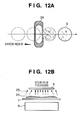
- FIG. 12A is a plan view showing magnetic field strength distribution and the film thickness on a substrate by utilizing the invention.
- Fig. 12B shows the magnetic field strength and film thickness distribution in the direction indicated by an arrow B in Fig. 12A .
- the amount of sputter particles from the two end faces of the target in the longitudinal direction is small, and hence the film thickness on each end face of the substrate tends to be smaller than that on the middle portion, as shown in Figs. 15 and 16 .
- magnetic field strength 25 (visually indicated in Figs. 12A and 12B ) on the two sides (two end portion areas) of the target 7 in the longitudinal direction, and the magnetic field strength 25 on the middle portion of the target 7 decreases, as shown in Figs. 12A and 12B .
- the amount of sputter particles 26 from the two sides of the target 7 in the longitudinal direction are increased. This makes it possible to improve the thickness distribution of a film deposited on a substrate surface which passes through the space on the target surface side without increasing the length of the target in the longitudinal direction, as shown in Fig. 17 .
- Fig. 13 is a view showing the placement relationship between the substrate 9 and the target 7.
- reference symbol W denotes the size of the target 7 in the longitudinal direction
- D the size of the target 7 in the transverse direction
- P the width of the film formation substrate 9 (wafer) in a direction perpendicular to the transport direction
- T the distance between the target 7 and the substrate 9 facing each other.
- P 200 mm
- W 600 mm
- D 130 mm
- T 80 mm.
- a film thickness distribution defined by Range/Mean ⁇ 3% could be obtained with the following dimensional relationship: 2.5 ⁇ W / P ⁇ 1.8 W / D ⁇ 4.5 6.3 ⁇ W / T ⁇ 4.5 That is, the effect of increasing the magnetic field strength at the two ends of the target in a direction perpendicular to the substrate scan direction can reduce the target length W and therefore, running costs.
- a magnetron unit which can easily and accurately adjust the film thickness distribution of a film formed on the entire surface of a substrate without increasing the size of the magnetron sputtering apparatus based on the inline scheme.
- the magnetron unit 8 according to each embodiment of the present invention can also be applied to a cathode magnet used in forming films for manufacturing an electronic device such as a large flat panel display (liquid crystal display), a thin-film solar panel, a microinductor, a magnetic printhead, a memory device using a magnetic thin film such as an MRAM (Magnetoresistive Random Access Memory), or the like.
- a cathode magnet used in forming films for manufacturing an electronic device such as a large flat panel display (liquid crystal display), a thin-film solar panel, a microinductor, a magnetic printhead, a memory device using a magnetic thin film such as an MRAM (Magnetoresistive Random Access Memory), or the like.
- a large rectangular target sputtering target
- a cathode magnet is placed on the opposite surface side to a sputtering target.
- cathode magnets have rectangular shapes like the magnetron unit 8 in each embodiment of the present invention. Note however that such a magnet has a size in the order of meters. In such a case as well, it is necessary to adjust the film thickness distribution by magnetic field adjustment using the magnetron unit. However, since the magnet itself is large, the repulsive (attracting force) force is large. It is therefore difficult to adjust a magnetic field by replacing and attaching/detaching a magnet in the conventional manner.
- Fig. 19A is a view showing an example which adjusts the magnetic field distribution by arranging a plurality of magnetron units 8 for sputtering target.
- Fig. 19B is a view showing an example in which when there are a plurality of sputtering targets; magnetic field adjustment is performed for each sputtering target by providing the magnetron unit 8 according to the present invention for each sputtering target.
- the magnetron unit 8 allows magnetic field adjustment without detaching any magnets by being used for a film formation step for the manufacture of an electronic device such as a large flat panel display (liquid crystal display), a thin-film solar panel, a microinductor, or a magnetic printhead, a memory device using a magnetic thin film such as an MRAM, or the like.
- an electronic device such as a large flat panel display (liquid crystal display), a thin-film solar panel, a microinductor, or a magnetic printhead, a memory device using a magnetic thin film such as an MRAM, or the like.
Landscapes
- Chemical & Material Sciences (AREA)
- Engineering & Computer Science (AREA)
- Chemical Kinetics & Catalysis (AREA)
- Materials Engineering (AREA)
- Mechanical Engineering (AREA)
- Metallurgy (AREA)
- Organic Chemistry (AREA)
- Physics & Mathematics (AREA)
- Plasma & Fusion (AREA)
- Analytical Chemistry (AREA)
- Physical Vapour Deposition (AREA)
Applications Claiming Priority (2)
| Application Number | Priority Date | Filing Date | Title |
|---|---|---|---|
| JP2007283438 | 2007-10-31 | ||
| PCT/JP2008/069799 WO2009057715A1 (ja) | 2007-10-31 | 2008-10-30 | マグネトロンユニット、マグネトロンスパッタリング装置及び電子デバイスの製造方法 |
Publications (2)
| Publication Number | Publication Date |
|---|---|
| EP2204469A1 true EP2204469A1 (de) | 2010-07-07 |
| EP2204469A4 EP2204469A4 (de) | 2012-03-28 |
Family
ID=40591099
Family Applications (1)
| Application Number | Title | Priority Date | Filing Date |
|---|---|---|---|
| EP08843409A Withdrawn EP2204469A4 (de) | 2007-10-31 | 2008-10-30 | Magnetroneinheit, magnetron-sputtering-vorrchtung und verfahren zur herstellung einer elektronischen vorrichtung |
Country Status (5)
| Country | Link |
|---|---|
| US (1) | US7785449B2 (de) |
| EP (1) | EP2204469A4 (de) |
| JP (2) | JP4314318B2 (de) |
| CN (1) | CN101595240B (de) |
| WO (1) | WO2009057715A1 (de) |
Families Citing this family (18)
| Publication number | Priority date | Publication date | Assignee | Title |
|---|---|---|---|---|
| JP4494523B2 (ja) * | 2007-11-09 | 2010-06-30 | キヤノンアネルバ株式会社 | インライン型ウェハ搬送装置および基板搬送方法 |
| US8048277B2 (en) * | 2008-08-18 | 2011-11-01 | Canon Anelva Corporation | Magnet unit and magnetron sputtering apparatus |
| EP2159304A1 (de) * | 2008-08-27 | 2010-03-03 | Nederlandse Organisatie voor toegepast- natuurwetenschappelijk onderzoek TNO | Vorrichtung und Verfahren zur Atomlagenabscheidung |
| JP5390330B2 (ja) * | 2008-10-16 | 2014-01-15 | キヤノンアネルバ株式会社 | 基板処理装置およびそのクリーニング方法 |
| JP5336151B2 (ja) * | 2008-10-31 | 2013-11-06 | キヤノンアネルバ株式会社 | 薄膜形成装置及び磁気記録媒体の製造方法 |
| JP2010106349A (ja) * | 2008-10-31 | 2010-05-13 | Canon Anelva Corp | スパッタ装置、薄膜形成装置及び磁気記録媒体の製造方法 |
| JP4473342B1 (ja) * | 2008-12-24 | 2010-06-02 | キヤノンアネルバ株式会社 | スパッタリング装置および成膜方法 |
| JP5280459B2 (ja) | 2008-12-25 | 2013-09-04 | キヤノンアネルバ株式会社 | スパッタリング装置 |
| CN101988188B (zh) * | 2009-07-30 | 2013-08-28 | 鸿富锦精密工业(深圳)有限公司 | 溅镀用磁控装置 |
| US8776542B2 (en) * | 2009-12-25 | 2014-07-15 | Canon Anelva Corporation | Cooling system |
| TWI456082B (zh) * | 2010-03-26 | 2014-10-11 | Univ Nat Sun Yat Sen | 磁控式電漿濺鍍機 |
| JP5873276B2 (ja) | 2010-12-27 | 2016-03-01 | キヤノンアネルバ株式会社 | 磁石ユニットおよびマグネトロンスパッタリング装置 |
| JP5688996B2 (ja) * | 2011-03-07 | 2015-03-25 | 株式会社神戸製鋼所 | プラズマ源及びこのプラズマ源を備えた成膜装置 |
| KR20140109427A (ko) | 2012-01-30 | 2014-09-15 | 미쓰비시덴키 가부시키가이샤 | 자기회로 |
| CN104357803B (zh) * | 2014-11-20 | 2017-02-22 | 昆山国显光电有限公司 | 磁控溅射磁铁系统及其控制方法和磁控溅射装置 |
| JP6313250B2 (ja) * | 2015-03-11 | 2018-04-18 | 東芝メモリ株式会社 | 半導体製造装置 |
| US11073912B2 (en) * | 2016-07-07 | 2021-07-27 | Sekisui Polymatech Co., Ltd. | Magnetic deformable member |
| WO2019234477A1 (en) * | 2018-06-08 | 2019-12-12 | Kenosistec S.R.L. | Machine for the deposition of material by the cathodic sputtering technique |
Citations (3)
| Publication number | Priority date | Publication date | Assignee | Title |
|---|---|---|---|---|
| US5980707A (en) * | 1998-12-18 | 1999-11-09 | Sierra Applied Sciences, Inc. | Apparatus and method for a magnetron cathode with moving magnet assembly |
| US20060065525A1 (en) * | 2004-09-28 | 2006-03-30 | Jurgen Weichart | Method for manufacturing magnetron coated substrates and magnetron sputter source |
| US20070051616A1 (en) * | 2005-09-07 | 2007-03-08 | Le Hienminh H | Multizone magnetron assembly |
Family Cites Families (13)
| Publication number | Priority date | Publication date | Assignee | Title |
|---|---|---|---|---|
| JPS59137965A (ja) | 1983-01-28 | 1984-08-08 | Canon Inc | 像形成装置 |
| JPS59137965U (ja) * | 1983-03-03 | 1984-09-14 | 日本真空技術株式会社 | マグネトロン型スパツタカソ−ド |
| JPH0375369A (ja) | 1989-08-18 | 1991-03-29 | Fuji Photo Film Co Ltd | スパッタリング装置 |
| JPH0375368A (ja) * | 1989-08-18 | 1991-03-29 | Fuji Photo Film Co Ltd | スパッタリング装置 |
| JPH05148639A (ja) * | 1991-11-22 | 1993-06-15 | Anelva Corp | マグネトロンカソード電極 |
| JPH0726202A (ja) | 1993-07-14 | 1995-01-27 | Dainippon Ink & Chem Inc | 水性塗料用樹脂組成物 |
| JPH09118980A (ja) | 1995-10-24 | 1997-05-06 | Fujitsu Ltd | スパッタリング装置用のマグネトロンユニット及びスパッタリング装置 |
| JPH1025572A (ja) * | 1996-07-11 | 1998-01-27 | Hitachi Ltd | マグネトロンスパッタ装置 |
| JP3585760B2 (ja) * | 1999-01-27 | 2004-11-04 | シャープ株式会社 | マグネトロンスパッタ装置 |
| BR0116951B1 (pt) * | 2001-03-27 | 2011-06-14 | evaporador de arco com guia magnÉtico poderoso para alvos tendo uma grande Área de superfÍcie. | |
| EP1710829A1 (de) * | 2005-04-05 | 2006-10-11 | Applied Films GmbH & Co. KG | Magnetanordnung für ein Planar-Magnetron |
| JP4959175B2 (ja) * | 2005-11-09 | 2012-06-20 | 株式会社アルバック | マグネトロンスパッタ電極及びマグネトロンスパッタ電極を備えたスパッタリング装置 |
| JP2007283438A (ja) | 2006-04-17 | 2007-11-01 | Ntt Electornics Corp | ブラスト加工方法 |
-
2008
- 2008-10-30 CN CN2008800028071A patent/CN101595240B/zh active Active
- 2008-10-30 EP EP08843409A patent/EP2204469A4/de not_active Withdrawn
- 2008-10-30 WO PCT/JP2008/069799 patent/WO2009057715A1/ja active Application Filing
- 2008-10-30 JP JP2009506456A patent/JP4314318B2/ja active Active
-
2009
- 2009-05-14 JP JP2009117227A patent/JP2009174061A/ja not_active Withdrawn
- 2009-06-03 US US12/477,510 patent/US7785449B2/en active Active
Patent Citations (3)
| Publication number | Priority date | Publication date | Assignee | Title |
|---|---|---|---|---|
| US5980707A (en) * | 1998-12-18 | 1999-11-09 | Sierra Applied Sciences, Inc. | Apparatus and method for a magnetron cathode with moving magnet assembly |
| US20060065525A1 (en) * | 2004-09-28 | 2006-03-30 | Jurgen Weichart | Method for manufacturing magnetron coated substrates and magnetron sputter source |
| US20070051616A1 (en) * | 2005-09-07 | 2007-03-08 | Le Hienminh H | Multizone magnetron assembly |
Non-Patent Citations (1)
| Title |
|---|
| See also references of WO2009057715A1 * |
Also Published As
| Publication number | Publication date |
|---|---|
| CN101595240A (zh) | 2009-12-02 |
| WO2009057715A1 (ja) | 2009-05-07 |
| JP4314318B2 (ja) | 2009-08-12 |
| JPWO2009057715A1 (ja) | 2011-03-10 |
| JP2009174061A (ja) | 2009-08-06 |
| EP2204469A4 (de) | 2012-03-28 |
| US20090236219A1 (en) | 2009-09-24 |
| US7785449B2 (en) | 2010-08-31 |
| CN101595240B (zh) | 2012-05-23 |
Similar Documents
| Publication | Publication Date | Title |
|---|---|---|
| US7785449B2 (en) | Magnetron unit, magnetron sputtering apparatus, and method of manufacturing electronic device | |
| US5855744A (en) | Non-planar magnet tracking during magnetron sputtering | |
| US7347919B2 (en) | Sputter source, sputtering device, and sputtering method | |
| KR101299724B1 (ko) | 마그네트론 스퍼터 캐소드 및 성막 장치 | |
| US20090277779A1 (en) | Magnetic field generating apparatus, magnetic field generating method, sputtering apparatus, and method of manufacturing device | |
| US20130032476A1 (en) | Rotary cathodes for magnetron sputtering system | |
| TWI421363B (zh) | Magnetron sputtering method | |
| EP1120811B1 (de) | Flaches Magnetron-Zerstäubungsgerät | |
| JPH0835064A (ja) | スパッタリング装置 | |
| KR102628392B1 (ko) | 스퍼터 성막 장치 및 스퍼터 성막 방법 | |
| US20080296142A1 (en) | Swinging magnets to improve target utilization | |
| JP2000239841A (ja) | スパッタリング方法と装置 | |
| US20060272935A1 (en) | Multiple scanning magnetrons | |
| JP2012077360A (ja) | カソードユニットおよび成膜装置 | |
| KR100963413B1 (ko) | 마그네트론 스퍼터링 장치 | |
| US7879210B2 (en) | Partially suspended rolling magnetron | |
| KR102632430B1 (ko) | 성막 장치, 성막 방법, 및 전자 디바이스의 제조 방법 | |
| CN212316233U (zh) | 一种磁控溅射设备 | |
| WO2024152498A1 (zh) | 用于pvd平面靶的磁控管装置与磁控溅射设备 | |
| CN101988188A (zh) | 溅镀用磁控装置 | |
| KR100437867B1 (ko) | 가변 자석 구조를 가진 캐소드 | |
| JP2023091411A (ja) | スパッタ装置 | |
| KR101002052B1 (ko) | 마그네트론 스퍼터링 장치 | |
| WO2018204570A1 (en) | Flexible adjustable return path magnet assembly and methods | |
| CN110770364A (zh) | 磁控溅射阴极系统 |
Legal Events
| Date | Code | Title | Description |
|---|---|---|---|
| PUAI | Public reference made under article 153(3) epc to a published international application that has entered the european phase |
Free format text: ORIGINAL CODE: 0009012 |
|
| 17P | Request for examination filed |
Effective date: 20090605 |
|
| AK | Designated contracting states |
Kind code of ref document: A1 Designated state(s): AT BE BG CH CY CZ DE DK EE ES FI FR GB GR HR HU IE IS IT LI LT LU LV MC MT NL NO PL PT RO SE SI SK TR |
|
| AX | Request for extension of the european patent |
Extension state: AL BA MK RS |
|
| DAX | Request for extension of the european patent (deleted) | ||
| A4 | Supplementary search report drawn up and despatched |
Effective date: 20120228 |
|
| RIC1 | Information provided on ipc code assigned before grant |
Ipc: H01J 37/34 20060101ALI20120222BHEP Ipc: C23C 14/56 20060101ALI20120222BHEP Ipc: C23C 14/35 20060101AFI20120222BHEP |
|
| STAA | Information on the status of an ep patent application or granted ep patent |
Free format text: STATUS: THE APPLICATION IS DEEMED TO BE WITHDRAWN |
|
| 18D | Application deemed to be withdrawn |
Effective date: 20120927 |