EP2201686B1 - Spannungsgesteuerter oszillator mit kaskadenemitterfolgerpufferstufen - Google Patents
Spannungsgesteuerter oszillator mit kaskadenemitterfolgerpufferstufen Download PDFInfo
- Publication number
- EP2201686B1 EP2201686B1 EP08840491.8A EP08840491A EP2201686B1 EP 2201686 B1 EP2201686 B1 EP 2201686B1 EP 08840491 A EP08840491 A EP 08840491A EP 2201686 B1 EP2201686 B1 EP 2201686B1
- Authority
- EP
- European Patent Office
- Prior art keywords
- vco
- transistor
- varactor
- diode
- voltage
- Prior art date
- Legal status (The legal status is an assumption and is not a legal conclusion. Google has not performed a legal analysis and makes no representation as to the accuracy of the status listed.)
- Not-in-force
Links
- 239000000872 buffer Substances 0.000 title claims description 24
- 230000010355 oscillation Effects 0.000 claims description 15
- 238000002955 isolation Methods 0.000 claims description 12
- 230000002441 reversible effect Effects 0.000 claims description 11
- 239000003990 capacitor Substances 0.000 claims description 9
- 230000000977 initiatory effect Effects 0.000 claims description 2
- 239000013078 crystal Substances 0.000 description 5
- 230000007423 decrease Effects 0.000 description 5
- 238000010586 diagram Methods 0.000 description 5
- 230000008859 change Effects 0.000 description 4
- 230000004048 modification Effects 0.000 description 4
- 238000012986 modification Methods 0.000 description 4
- 230000008878 coupling Effects 0.000 description 3
- 238000010168 coupling process Methods 0.000 description 3
- 238000005859 coupling reaction Methods 0.000 description 3
- 230000000295 complement effect Effects 0.000 description 2
- 239000000463 material Substances 0.000 description 2
- 239000004065 semiconductor Substances 0.000 description 2
- 230000004913 activation Effects 0.000 description 1
- 230000002411 adverse Effects 0.000 description 1
- 238000004891 communication Methods 0.000 description 1
- 230000003247 decreasing effect Effects 0.000 description 1
- 230000000694 effects Effects 0.000 description 1
- 230000007613 environmental effect Effects 0.000 description 1
- 230000007717 exclusion Effects 0.000 description 1
- 238000007667 floating Methods 0.000 description 1
- 230000000670 limiting effect Effects 0.000 description 1
- 238000000034 method Methods 0.000 description 1
- 230000036961 partial effect Effects 0.000 description 1
- 230000000737 periodic effect Effects 0.000 description 1
- 229920000729 poly(L-lysine) polymer Polymers 0.000 description 1
- 239000010453 quartz Substances 0.000 description 1
- 230000009467 reduction Effects 0.000 description 1
- 230000035945 sensitivity Effects 0.000 description 1
- VYPSYNLAJGMNEJ-UHFFFAOYSA-N silicon dioxide Inorganic materials O=[Si]=O VYPSYNLAJGMNEJ-UHFFFAOYSA-N 0.000 description 1
- 238000004088 simulation Methods 0.000 description 1
- 238000004804 winding Methods 0.000 description 1
Images
Classifications
-
- H—ELECTRICITY
- H03—ELECTRONIC CIRCUITRY
- H03L—AUTOMATIC CONTROL, STARTING, SYNCHRONISATION OR STABILISATION OF GENERATORS OF ELECTRONIC OSCILLATIONS OR PULSES
- H03L7/00—Automatic control of frequency or phase; Synchronisation
- H03L7/06—Automatic control of frequency or phase; Synchronisation using a reference signal applied to a frequency- or phase-locked loop
- H03L7/08—Details of the phase-locked loop
- H03L7/099—Details of the phase-locked loop concerning mainly the controlled oscillator of the loop
-
- H—ELECTRICITY
- H03—ELECTRONIC CIRCUITRY
- H03B—GENERATION OF OSCILLATIONS, DIRECTLY OR BY FREQUENCY-CHANGING, BY CIRCUITS EMPLOYING ACTIVE ELEMENTS WHICH OPERATE IN A NON-SWITCHING MANNER; GENERATION OF NOISE BY SUCH CIRCUITS
- H03B5/00—Generation of oscillations using amplifier with regenerative feedback from output to input
- H03B5/02—Details
- H03B5/04—Modifications of generator to compensate for variations in physical values, e.g. power supply, load, temperature
-
- H—ELECTRICITY
- H03—ELECTRONIC CIRCUITRY
- H03B—GENERATION OF OSCILLATIONS, DIRECTLY OR BY FREQUENCY-CHANGING, BY CIRCUITS EMPLOYING ACTIVE ELEMENTS WHICH OPERATE IN A NON-SWITCHING MANNER; GENERATION OF NOISE BY SUCH CIRCUITS
- H03B5/00—Generation of oscillations using amplifier with regenerative feedback from output to input
- H03B5/08—Generation of oscillations using amplifier with regenerative feedback from output to input with frequency-determining element comprising lumped inductance and capacitance
- H03B5/12—Generation of oscillations using amplifier with regenerative feedback from output to input with frequency-determining element comprising lumped inductance and capacitance active element in amplifier being semiconductor device
- H03B5/1206—Generation of oscillations using amplifier with regenerative feedback from output to input with frequency-determining element comprising lumped inductance and capacitance active element in amplifier being semiconductor device using multiple transistors for amplification
- H03B5/1218—Generation of oscillations using amplifier with regenerative feedback from output to input with frequency-determining element comprising lumped inductance and capacitance active element in amplifier being semiconductor device using multiple transistors for amplification the generator being of the balanced type
-
- H—ELECTRICITY
- H03—ELECTRONIC CIRCUITRY
- H03B—GENERATION OF OSCILLATIONS, DIRECTLY OR BY FREQUENCY-CHANGING, BY CIRCUITS EMPLOYING ACTIVE ELEMENTS WHICH OPERATE IN A NON-SWITCHING MANNER; GENERATION OF NOISE BY SUCH CIRCUITS
- H03B5/00—Generation of oscillations using amplifier with regenerative feedback from output to input
- H03B5/08—Generation of oscillations using amplifier with regenerative feedback from output to input with frequency-determining element comprising lumped inductance and capacitance
- H03B5/12—Generation of oscillations using amplifier with regenerative feedback from output to input with frequency-determining element comprising lumped inductance and capacitance active element in amplifier being semiconductor device
- H03B5/1231—Generation of oscillations using amplifier with regenerative feedback from output to input with frequency-determining element comprising lumped inductance and capacitance active element in amplifier being semiconductor device the amplifier comprising one or more bipolar transistors
-
- H—ELECTRICITY
- H03—ELECTRONIC CIRCUITRY
- H03B—GENERATION OF OSCILLATIONS, DIRECTLY OR BY FREQUENCY-CHANGING, BY CIRCUITS EMPLOYING ACTIVE ELEMENTS WHICH OPERATE IN A NON-SWITCHING MANNER; GENERATION OF NOISE BY SUCH CIRCUITS
- H03B5/00—Generation of oscillations using amplifier with regenerative feedback from output to input
- H03B5/08—Generation of oscillations using amplifier with regenerative feedback from output to input with frequency-determining element comprising lumped inductance and capacitance
- H03B5/12—Generation of oscillations using amplifier with regenerative feedback from output to input with frequency-determining element comprising lumped inductance and capacitance active element in amplifier being semiconductor device
- H03B5/1237—Generation of oscillations using amplifier with regenerative feedback from output to input with frequency-determining element comprising lumped inductance and capacitance active element in amplifier being semiconductor device comprising means for varying the frequency of the generator
- H03B5/124—Generation of oscillations using amplifier with regenerative feedback from output to input with frequency-determining element comprising lumped inductance and capacitance active element in amplifier being semiconductor device comprising means for varying the frequency of the generator the means comprising a voltage dependent capacitance
- H03B5/1243—Generation of oscillations using amplifier with regenerative feedback from output to input with frequency-determining element comprising lumped inductance and capacitance active element in amplifier being semiconductor device comprising means for varying the frequency of the generator the means comprising a voltage dependent capacitance the means comprising voltage variable capacitance diodes
-
- H—ELECTRICITY
- H03—ELECTRONIC CIRCUITRY
- H03L—AUTOMATIC CONTROL, STARTING, SYNCHRONISATION OR STABILISATION OF GENERATORS OF ELECTRONIC OSCILLATIONS OR PULSES
- H03L1/00—Stabilisation of generator output against variations of physical values, e.g. power supply
- H03L1/02—Stabilisation of generator output against variations of physical values, e.g. power supply against variations of temperature only
- H03L1/022—Stabilisation of generator output against variations of physical values, e.g. power supply against variations of temperature only by indirect stabilisation, i.e. by generating an electrical correction signal which is a function of the temperature
-
- H—ELECTRICITY
- H03—ELECTRONIC CIRCUITRY
- H03B—GENERATION OF OSCILLATIONS, DIRECTLY OR BY FREQUENCY-CHANGING, BY CIRCUITS EMPLOYING ACTIVE ELEMENTS WHICH OPERATE IN A NON-SWITCHING MANNER; GENERATION OF NOISE BY SUCH CIRCUITS
- H03B2200/00—Indexing scheme relating to details of oscillators covered by H03B
- H03B2200/006—Functional aspects of oscillators
- H03B2200/0094—Measures to ensure starting of oscillations
Definitions
- This invention relates generally to voltage controlled oscillators (VCOs), and more particularly, to a VCO having cascaded emitter follower buffer stages.
- VCOs voltage controlled oscillators
- VCOs typically have to operate in narrow frequency bands. For example, in some Industrial, Scientific and Medical (ISM) applications VCOs may have to operate in a 120 MHz frequency window. VCOs are typically phase locked to an input signal using a phase locked loop (PLL) that includes a feedback to control the output frequency of the VCO. The PLL maintains the VCO in the narrow frequency band.
- PLL phase locked loop
- VCOs are used in many different applications.
- VCOs are used in transmitters to control the operating frequency of the transmitters.
- high frequency applications for example, when using a 24 GHz VCO, such as, used in automotive or other short range radars, isolation between the VCO and the other portions of the transmitter is an issue.
- the frequency of the VCO is changed, often referred to as frequency pulling, as a result of varying load conditions.
- the varying load conditions may be caused, for example, by a change in environmental conditions, such as from varying reflections from a changing environment near the antenna, or by other circuits connected to the VCO changing the operating mode or state.
- the turning on/off of the switches in a pulsed radar transmitter may vary the load impedance presented to the VCO.
- These changes in load-impedance (and hence frequency) can occur within nanoseconds at a rate that the PLL cannot correct.
- the operating frequency of the VCO will thus be affected and that may cause the VCO to operate outside of a desired or required frequency band, as well as having other affects on circuit performance, which may be less detectable.
- US2006226923 relates to an oscillator circuit comprising resonator means and, first and second emitter followers being symmetrically coupled to the resonator means and been connected to further emitter followers for providing capacitive loading.
- JP08274540 provides an oscillator of a simple circuit configuration without requiring a special circuit element by connecting an electrostatic capacitor for connecting the emitters of transistors consisting of a differential pair, and grounding its almost midpoint.
- CONSTITUTION An oscillator circuit OSC is oscillated as a Colpitts oscillator circuit of the differential pair disconnected from a coil L5 for oscillation with a midpoint tap of a resonance circuit RSN and a node 7 through electrostatic capacitors C10 and C11 for coupling. As a result, the respective terminals of the bases and emitters of transistors(Tr) Q1 and 02 for oscillation are turned to the phase state of ⁇ 90 deg. from the ground potential.
- phase midpoint of a completely balanced oscillator circuit is really grounded by adopting a simple circuit configuration shared with the OSC and RSN, and an oscillation carrier is prevented from being discharged.
- the circuit configuration of the oscillator defining the ground potential as a balanced point is prepared and the reverse phase state of the Tr for oscillation is more exactly provided.
- DE2460762 discloses a transistor based tunable high frequency oscillator which provides a considerable output frequency range but still has very low harmonic content, is used, and a compromise between these conflicting features is attained. It consists of a two transistor (T1, T2) oscillator circuit arranged in a symmetrical configuration using inductances (L1, L2) capacitances (C1, C4) and tuned capacitances (D1, D2, D3, D4) consisting of capacitances (C1, C4) and tuned capacitances (D1, D2, D3, D4) consisting of capacitance diodes in the feedback networks.
- the output is taken from a winding (LK) associated with the inductances (L, L2), and the output frequency is determined, typically between 160 MHz and 380 MHz, by a voltage applied to these diodes by suitable resistors (R2 R9).
- LK winding
- R2 R9 resistors
- US5937340 relates to an oscillator OSC intended to provide an output signal having a frequency which is variable as a function of a tuning voltage Vtun.
- the oscillator OSC includes a passive part having two series-arranged variable capacitances Cs, biased by the tuning voltage Vtun, and connected to a power supply VCC via two inductances Lext, and an active part having a first transistor T1 and a second transistor T2 whose collectors are connected to the output terminals C1 and C2 of the passive part, the base of one transistor being connected to the collector of the other transistor via a coupling capacitor Cfb.
- the passive part includes two high-pass filters, each being inserted between one of the output terminals S1 or S2 and one of the variable capacitances Cs, which allows a reduction of the active part's sensitivity to low-frequency noise.
- US2005128017 discloses a variable frequency oscillator having multiple, independent frequency control inputs, each coupled to a respective tuning sub-circuit.
- the tuning sub-circuits are connected in parallel with each other and with a resonator module, which may be a quartz crystal, inductor, or other reactance component.
- Each tuning sub-circuit consists of two varactors with their respective cathodes coupled to each other and to their corresponding frequency control input.
- the overall frequency pull range of each frequency control input remains unaffected by the activation of any other frequency control input.
- at least one frequency control input is a temperature compensation control input that can maintain the variable oscillator insensitive to temperature variations while the remaining frequency control inputs provide functional frequency control.
- EP1471632 relates to a crystal oscillator circuit in which the output level is maintained to prevent changes in oscillation frequency due to variations in power voltage.
- This crystal oscillator circuit comprises a resonance circuit formed of a crystal oscillator (which acts as an inductor component) and dividing capacitors, an oscillation amplifier formed of ECL circuitry driven by a power voltage connected to the resonance circuit, and a pull-down resistor between an output terminal of the ECL circuit and ground.
- the pull-down resistor acts as serially-connected dividing resistors and also a bias capacitor is provided between a connection point between those dividing resistors and ground.
- the present invention also relates to a frequency-switching oscillator having a simple circuit design and a small number of components.
- This frequency switching oscillator enables a configuration in which an oscillation amplifier that is a two input, two output type of ECL circuit having mutually inverted signals is connected to a resonance circuit formed of a crystal oscillator and dividing capacitors, a first resonance circuit provided with a first electronic switch is connected between one pair of input-output terminals for mutually inverted signals of the ECL circuit; a second resonance circuit is connected between another pair of input-output terminals for mutually inverted signals of the ECL circuit; and the resonance frequencies of the first and second resonance circuits are different and also the first and second electronic switches are switched to select one of the resonance circuits.
- a voltage controlled oscillator (VCO) suitable for a phase locked loop comprising: an LC resonator having a varactor diode: a varactor bias network including the varactor-diode the anode of the varactor diode being connected to a variable voltage and the cathode of the varactor-diode being connected to a pull-down resistor network, the pull-down resistor network having a first resistor, a second resistor and a third resistor, wherein the first and second resistors form a voltage divider, with one end of the third resistor being connected between the first and second resistors, and the other end of the third resistor having an input for connecting to the phase locked loop, the pull-down resistor network being configured to generate an internal bias voltage suitable for initiating oscillation in the VCO in the absence of an input signal from the phase locked loop by applying a reverse bias to the varactor-diode; and an output buffer arranged to provide isolation of the VCO.
- VCO voltage controlled oscillator
- VCO voltage controlled oscillator
- the VCO also includes a resistor network (shown in Figure 3 ) to provide self-oscillation of the VCO under certain conditions.
- a temperature bias control (shown in Figure 4 ) that is counter proportional to temperature is also provided in combination with the VCO.
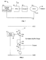
- a VCO 20 is provided that may form part of a phase locked loop (PLL) 22 as shown in Figure 1 .
- the PLL 22 includes a charge pump 24, the input of which is connected to the output of a phase frequency detector (PFD) 26.
- the input of the PFD 26 is connected to the output of a frequency divider 28.
- the input of the frequency divider 28 is connected to the VCO 20.
- a loop 30 is also provided from the output of the charge pump 24 to the control input of the VCO 20.
- the VCO 20 may be provided in connection with different PLLs having different components parts.
- the VCO 20 also may be used in different applications having different operating requirements.
- the VCO 20 may be used as part of a PLL in radio, telecommunications, computers and other electronic applications to generate stable frequencies (e.g., a frequency synthesizer) or to recover a signal from a noisy communication channel.
- the PLL 22 may be implemented in hardware, for example, a single integrated circuit chip, in software, or in combination thereof.
- the phase of the VCO 20 at an output 32 is locked using the PLL 22 and based on an input signal, for example, an input frequency signal (Fref) received at the PFD 26.
- the PLL 22 is essentially an electronic control system that generates a signal that is locked to the phase of the input or reference signal.
- the PLL 22 responds to both the frequency and the phase of the input signal and automatically increases or decreases the frequency of the VCO 20 until the output frequency of the VCO 20 is matched to the reference signal (times a divider ratio) in both frequency and phase (which may include an acceptable deviation).
- the VCO 20 generates a periodic output signal and the charge pump 24 sends a control signal to the VCO 20 based on feedback from the loop 30.
- the control voltage of the charge pump 24 is changed based on the change in frequency as detected by the PFD 26.
- the frequency of the VCO 20 is accordingly increased (e.g., oscillation speeds up). If the phase moves ahead, the control voltage is again changed, but to decrease the frequency of the VCO 20 (e.g., oscillation slows down).
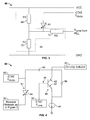
- the VCO 20 includes a plurality of transistors 40a and 40b provided in a cascaded configuration that defines a combined buffer stage 42 as shown in Figure 2 (illustrating a more detailed partial schematic of the VCO 20).
- the transistors 40a and 40b are connected in an arrangement forming buffer stages that are connected to a VCO core 21.
- the two transistors 40a and 40b are connected in a cascaded configuration such that the first transistor 40a defines a first buffer stage connected in a cascaded configuration with the second transistor 40b that defines a second buffer stage.
- additional transistors 40a and 40b may be added to the cascaded configuration to thereby define additional buffer stages 42.
- the transistors 40a and 40b may be, for example, bipolar junction transistors (BJTs) provided in an NPN configuration.
- BJTs bipolar junction transistors
- a base 44 of the first transistor 40a is connected to the output of the VCO core 21 through a capacitor 25 and a collector 46 of the first transistor 40a is connected to power (e.g., 5 volt also designated and commonly referred to as Vcc).
- An emitter 48 of the first transistor 40a is connected to a collector 50 of the second transistor 40b.
- a base 52 of the second transistor 40b is connected to the collector 50 of the second transistor 40b.
- An emitter 54 of the second transistor 40b is connected to ground through a current source 56.
- An output is provided at the emitter 54 of the second transistor 40b.
- the transistors 40a and 40b are provided in a common emitter/source follower arrangement that isolates the VCO core 21 from the output.
- both stages of the combined buffer stage 42 namely the transistors 40a and 40b share the same current.
- the buffer stages are AC coupled to the VCO core 21.
- the reverse isolation is determined by the intrinsic base/emitter junction capacitance of the transistor(s).
- the reverse isolation is determined by the series combination of two intrinsic base/emitter junction capacitances. Accordingly, this arrangement reduces the capacitance by half and thus doubles the reverse isolation if transistors 40a and 40b are of the same size.
- the output voltage swing in this cascaded configuration is the same as that in the conventional emitter follower such that the loss through the buffer stage is minimized.
- the two transistors 40a and 40b use a common bias current. Therefore, this arrangement consumes the same DC power as the conventional emitter follower while providing improved reverse isolation.
- the VCO core 21 includes a varactor bias network 60 as shown in Figure 3 . It should be noted that only half of the differential circuit is shown.
- the varactor bias network 60 includes a varactor-diode 64 that is essentially a diode that has a variable capacitance that is a function of the voltage applied to the terminals of the varactor-diode 64, for example, a complementary to absolute temperature (CTAT) Vdiode voltage as described in more detail below.
- CTAT complementary to absolute temperature
- the varactor bias network 60 in accordance with various embodiments includes a pull-down resistor network 66 having a first resistor 68, a second resistor 70 and a third resistor 72.
- the first and second resistors 68 and 70 form a voltage divider with one end of the third resistor 72 connected between the first and second resistors 68 and 70.
- the other end of third resistor 72 is connected to a control voltage (Vtune) from the PLL 22, for example, a control voltage from the charge pump 24.
- the first and second resistors 68 and 70 are connected between Vcc (e.g., 5 volts) and ground (GND).
- the voltage applied to the varactor-diode 64 is variable. In various embodiments, the voltage applied to the varactor-diode 64 is counter proportional to changes in temperature as described in more detail below.
- the resistor network 66 of the varactor bias network 60 ensures that the VCO 20 does not enter a dead lock condition if no signal is received from the charge pump 24.
- the Quality-factor of the varactor-diode 64 decreases as the reverse bias on the varactor-diode 64 decreases.
- the VCO 20 may not be able to start proper oscillation. When this occurs, the VCO 20 typically will enter a dead lock condition if the PLL 22 does not send a proper voltage to activate the VCO 20.
- the varactor-diode 64 when this condition occurs, where the charge pump 24 sends no signal to the VCO 20 (e.g., Vtune in Figure 3 is floating), the varactor-diode 64 will be biased, for example, to 2 volts internally to begin oscillation of the VCO 20. The voltage is determined by the values of the resistors 68, 70 and 72 of the resistor network 66. Thereafter, once the oscillation of the VCO 20 begins and the PFD 26 receives an RF signal from the VCO 20 as a result of the oscillation, the PLL 22 will begin normal operation. The PLL 22 essentially starts operating based on the internal voltage generated by the varactor bias network 60 having the resistor network 66. The varactor-diode 64 will then be biased at the proper voltage according to the voltage from the charge pump 24 and the resistor ratios of the resistor network 66. Thus, self-starting or self-oscillating operation is provided.
- a temperature bias circuit 80 as shown in Figure 4 that also forms part of the VCO core 21 (shown in Figure 2 ). It should be noted that only half of the differential circuit is shown in Figure 4 .
- a control voltage illustrated as a compensated bias voltage 82 (e.g., complementary to absolute temperature (CTAT) Vdiode voltage) is applied to the varactor-diode 64 and another control voltage, illustrated as a compensated bias voltage 84 (CTAT Vcore) is applied to a transistor 86 (e.g., a heterojunction bipolar transistor (HBT) transistor), which is the core transistor of the VCO core 21 as shown in Figure 5 .
- a plurality of capacitors 88 are also included to provide AC coupling.
- a CTAT voltage created as the build-in potential in a semiconductor p-n junction is counter proportional to the temperature as described below.
- An emitter 92 of the transistor 86 is also connected through a current source 94 to ground and a collector 93 of the transistor 86 is connected to an inductor 62.
- C q ⁇ ⁇ s 2 ⁇ 1 N a + 1 N d ⁇ ⁇ + V reverse - bias 1 2
- N a and N d are the doping concentrations of the p-type and n-type semiconductor
- ⁇ is the build-in potential across the p and n regions
- V reverse-bias is the reverse bias applied on the p-n junction
- ⁇ s is the surface potential
- q is the electron charge.
- the CTAT bias circuit 80 is used to bias a base 90 of the transistor 86 and an anode 91 of the varactor-diode 64.
- the compensation is counter proportional to temperature. For example, as temperature increases the CTAT voltage decreases as based on predetermined values (e.g., values based on empirical analysis and/or circuit simulations).
- the bias voltages of the transistor 86 and varactor-diode 64 are adjusted to minimize the change in junction capacitance, which determines the frequency shift over temperature.
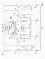
- a VCO 20 is provided as shown in Figure 5 , illustrating a complete schematic of the VCO 20 having the VCO core 21, the combined buffer stage 42 (also shown in Figure 2 ), the resistor network 66 (also shown in Figure 3 ), and the temperature bias circuit 80 (also shown in Figure 4 ).
- the VCO 20 may be provided, for example, on a single chip (e.g., integrated circuit chip) and have a differential circuit design. It should be noted that Figure 5 shows both halves of the differential circuit.
- the VCO 20 includes output buffers having a cascaded emitter follower configuration that defines a combined buffer stage 42 of transistors connected in parallel and connected to the VCO core 21. This output buffer configuration provides improved isolation without increasing DC power requirements.
- the VCO core 21 also includes a pull-down resistor network 66 that ensures that the PLL 22 does not enter a dead lock condition when no signal is received from the charge pump 24. Accordingly, a self-starting VCO 20 is provided. Additionally, a counter proportional temperature compensation is provided to both the varactor-diode 64 and the transistor 86 to provide improved compensation for temperature shift.
Landscapes
- Inductance-Capacitance Distribution Constants And Capacitance-Resistance Oscillators (AREA)
- Stabilization Of Oscillater, Synchronisation, Frequency Synthesizers (AREA)
Claims (6)
- Spannungsgesteuerter Oszillator (VCO) (20), geeignet für eine Phasenregelschleife, umfassend:einen LC-Resonator, der eine Varaktordiode aufweist:ein Varaktorvorspannnetz (60), welches die Varaktordiode (64) umfasst, wobei die Anode der Varaktordiode mit einer variablen Spannung verbunden ist und die Kathode der Varaktordiode mit einem Pull-down-Widerstandsnetz (66) verbunden ist, wobei das Pull-down-Widerstandsnetz einen ersten Widerstand (68), einen zweiten Widerstand (70) und einen dritten Widerstand (72) aufweist, wobei der erste (68) und zweite (70) Widerstand einen Spannungsteiler bilden, wobei ein Ende des ersten Widerstands (72) zwischen dem ersten (68) und zweiten (70) Widerstand angeschlossen ist und das andere Ende des dritten Widerstands (72) einen Eingang zum Anschließen an die Phasenregelschleife aufweist,wobei das Pull-down-Widerstandsnetz dafür konfiguriert ist, eine interne Vorspannung zu erzeugen, die zum Initiieren einer Oszillation in dem VCO in der Abwesenheit eines Eingangssignals von der Phasenregelschleife durch ein Anlegen einer Sperrspannung an die Varaktordiode geeignet ist; undeinen Ausgangspuffer (42), der dafür eingerichtet ist, eine Isolation des VCO bereitzustellen.
- VCO nach Anspruch 1, wobei die interne Vorspannung ungefähr 2 Volt beträgt.
- VCO nach Anspruch 1 oder Anspruch 2, wobei der LC-Resonator ferner eine erste Temperaturkompensations-Vorspannungsquelle (82) umfasst, die eine Temperaturkompensations-Vorspannung an eine Anode (91) der Varaktordiode anlegt, und wobei die erste Temperaturkompensations-Vorspannungsquelle zu Änderungen in der Temperatur umgekehrt proportional ist.
- VCO nach einem der vorhergehenden Ansprüche, ferner umfassend einen Transistor (86) und eine zweite Temperaturkompensations-Vorspannungsquelle (84), die eine Temperaturkompensations-Vorspannung an eine Basis (90) des Transistors anlegt, und wobei die zweite Temperaturkompensations-Vorspannungsquelle umgekehrt proportional zu Änderungen in der Temperatur ist, wobei ein Kollektor (93) des Transistors mit dem Varaktor-Vorspannungsnetz wechselspannungsgekoppelt ist.
- VCO nach einem der Ansprüche 1 bis 4, wobei der Ausgangspuffer umfasst:eine erste Pufferstufe, die einen ersten Transistor (40a) umfasst; undeine zweite Pufferstufe, die einen zweiten Transistor (40b) umfasst, wobei eine Basis (44) des ersten Transistors (40a) über einen Kondensator (25) mit dem Ausgang des VCO-Kerns (21) verbunden ist; ein Kollektor (46) des ersten Transistor (40a) mit einer Energiequelle (Vcc) verbunden ist; ein Emitter (48) des ersten Transistors (40a) mit einem Kollektor (50) des zweiten Transistors (40b) verbunden ist, eine Basis (52) des zweiten Transistors (40b) mit dem Kollektor (50) des zweiten Transistors (40b) verbunden ist; ein Emitter (54) des zweiten Transistors (40b) über eine Stromquelle (56) mit Masse verbunden ist und ein Ausgang an dem Emitter (54) des zweiten Transistors (40b) bereitgestellt ist.
- VCO nach Anspruch 5, wobei der erste und zweite Transistor (40a, 40b) für einen Betrieb bei ungefähr 24 GHz ausgelegt sind.
Applications Claiming Priority (2)
| Application Number | Priority Date | Filing Date | Title |
|---|---|---|---|
| US11/873,793 US7791422B2 (en) | 2007-10-17 | 2007-10-17 | Voltage controlled oscillator with cascaded emitter follower buffer stages |
| PCT/US2008/080165 WO2009052289A1 (en) | 2007-10-17 | 2008-10-16 | Voltage controlled oscillator with cascaded emitter follower buffer stages |
Publications (3)
| Publication Number | Publication Date |
|---|---|
| EP2201686A1 EP2201686A1 (de) | 2010-06-30 |
| EP2201686A4 EP2201686A4 (de) | 2012-11-14 |
| EP2201686B1 true EP2201686B1 (de) | 2015-01-07 |
Family
ID=40562895
Family Applications (1)
| Application Number | Title | Priority Date | Filing Date |
|---|---|---|---|
| EP08840491.8A Not-in-force EP2201686B1 (de) | 2007-10-17 | 2008-10-16 | Spannungsgesteuerter oszillator mit kaskadenemitterfolgerpufferstufen |
Country Status (4)
| Country | Link |
|---|---|
| US (1) | US7791422B2 (de) |
| EP (1) | EP2201686B1 (de) |
| JP (2) | JP2011501574A (de) |
| WO (1) | WO2009052289A1 (de) |
Families Citing this family (8)
| Publication number | Priority date | Publication date | Assignee | Title |
|---|---|---|---|---|
| US7777585B1 (en) * | 2008-06-25 | 2010-08-17 | Silicon Laboratories Inc. | Passive temperature compensation for an oscillator |
| US8717115B2 (en) * | 2012-01-13 | 2014-05-06 | Xilinx, Inc. | Resonator circuit and method of generating a resonating output signal |
| US9331698B2 (en) | 2014-01-02 | 2016-05-03 | Freescale Semiconductor, Inc. | Level shifter circuit |
| CN105897246B (zh) | 2014-12-26 | 2020-10-02 | 恩智浦美国有限公司 | 用于高电压应用的电压电平移位器 |
| WO2016160729A1 (en) * | 2015-03-27 | 2016-10-06 | Si-Ware Systems | Compensating temperature null characteristics of self-compensated oscillators |
| US9438249B1 (en) | 2015-09-21 | 2016-09-06 | Qualcomm Incorporated | Resonant circuit temperature compensation |
| EP3190706A1 (de) * | 2016-01-07 | 2017-07-12 | Sdrf Eurl | Oszillator mit variabler frequenz mit grossem abstimmbereich und geringem phasenrauschen |
| US12423253B2 (en) * | 2023-01-25 | 2025-09-23 | Micron Technology, Inc. | Current-controlled buffer using analog bias |
Citations (1)
| Publication number | Priority date | Publication date | Assignee | Title |
|---|---|---|---|---|
| US3573646A (en) * | 1969-07-17 | 1971-04-06 | Us Air Force | High stability emitter follower |
Family Cites Families (31)
| Publication number | Priority date | Publication date | Assignee | Title |
|---|---|---|---|---|
| DE2460762B1 (de) * | 1974-12-21 | 1976-04-22 | Philips Patentverwaltung | Schaltungsanordnung fuer einen HF-Oszillator |
| JPS5426601A (en) * | 1977-08-01 | 1979-02-28 | Pioneer Electronic Corp | Temperature compensating circuit for varactor |
| US4843265A (en) * | 1986-02-10 | 1989-06-27 | Dallas Semiconductor Corporation | Temperature compensated monolithic delay circuit |
| US5254955A (en) * | 1989-08-25 | 1993-10-19 | Anritsu Corporation | Advanced phase locked loop circuit |
| JPH0834384B2 (ja) * | 1990-02-08 | 1996-03-29 | 富士通株式会社 | マイクロ波発振器 |
| JPH0653739A (ja) * | 1992-07-28 | 1994-02-25 | Sharp Corp | 電圧制御発振器 |
| US5245298A (en) * | 1992-07-30 | 1993-09-14 | Motorola, Inc. | Voltage controlled oscillator having cascoded output |
| KR960003560B1 (ko) * | 1992-11-26 | 1996-03-15 | 삼성전기주식회사 | 전압제어 발진회로 |
| BE1007477A3 (nl) * | 1993-09-06 | 1995-07-11 | Philips Electronics Nv | Oscillator. |
| DE4334079C2 (de) * | 1993-10-06 | 1997-02-13 | Daimler Benz Aerospace Ag | Hochgenauer Radar-Entfernungsmesser |
| JPH0846427A (ja) * | 1994-07-29 | 1996-02-16 | Kyocera Corp | 電圧制御型水晶発振器 |
| US5650754A (en) * | 1995-02-15 | 1997-07-22 | Synergy Microwave Corporation | Phase-loched loop circuits and voltage controlled oscillator circuits |
| JPH08274540A (ja) * | 1995-03-31 | 1996-10-18 | Sony Corp | 発振器 |
| US5621362A (en) * | 1996-02-05 | 1997-04-15 | Motorola, Inc. | Cascode oscillator having optimum phase noise and bandwidth performance |
| DE69718741T2 (de) * | 1996-10-10 | 2003-11-13 | Koninklijke Philips Electronics N.V., Eindhoven | Integrierter Oszillator und einen solchen Oszillator verwendendes Funktelefon |
| US5847614A (en) * | 1996-11-15 | 1998-12-08 | Analog Devices, Inc. | Low power charge pump |
| JPH1155034A (ja) * | 1997-08-06 | 1999-02-26 | Nec Corp | 電圧制御発振器 |
| JP3697847B2 (ja) * | 1997-08-21 | 2005-09-21 | ソニー株式会社 | 電圧制御発振回路 |
| JPH1168462A (ja) * | 1997-08-22 | 1999-03-09 | Toyo Commun Equip Co Ltd | 圧電発振回路 |
| US5986514A (en) * | 1998-01-26 | 1999-11-16 | Motorola, Inc. | Self-biased voltage controlled oscillator (VCO) method and apparatus |
| US6204784B1 (en) * | 2000-04-21 | 2001-03-20 | Raytheon Company | Multiple analog to digital converter clock phase alignment technique using varactor diodes |
| JP3863753B2 (ja) * | 2000-11-06 | 2006-12-27 | 三洋電機株式会社 | 電圧制御型発振器および通信装置 |
| US6417740B1 (en) * | 2001-02-22 | 2002-07-09 | Chartered Semiconductor Manufacturing Ltd. | Wide-band/multi-band voltage controlled oscillator |
| WO2002088639A1 (en) * | 2001-04-27 | 2002-11-07 | Mykrolis Corporation | System and method for filtering output in mass flow controllers and mass flow meters |
| JP2003298349A (ja) * | 2002-04-03 | 2003-10-17 | Matsushita Electric Ind Co Ltd | 電圧制御型発振回路 |
| EP1597819A1 (de) * | 2003-02-20 | 2005-11-23 | Koninklijke Philips Electronics N.V. | Oszillatorschaltung |
| US7075381B2 (en) * | 2003-04-15 | 2006-07-11 | Nihon Dempa Kogyo Co., Ltd. | Oscillator circuit and oscillator |
| US7167058B2 (en) * | 2003-12-11 | 2007-01-23 | Seiko Epson Corporation | Temperature compensation for a variable frequency oscillator without reducing pull range |
| JP2007096523A (ja) * | 2005-09-27 | 2007-04-12 | Epson Toyocom Corp | 電圧制御発振器 |
| EP1783913A1 (de) * | 2005-11-08 | 2007-05-09 | Deutsche Thomson-Brandt Gmbh | Schaltbarer PLL Schaltkreis mit zwei Loops |
| JP4550726B2 (ja) * | 2005-12-01 | 2010-09-22 | 三菱電機株式会社 | 電圧制御発振器 |
-
2007
- 2007-10-17 US US11/873,793 patent/US7791422B2/en active Active
-
2008
- 2008-10-16 JP JP2010530112A patent/JP2011501574A/ja active Pending
- 2008-10-16 EP EP08840491.8A patent/EP2201686B1/de not_active Not-in-force
- 2008-10-16 WO PCT/US2008/080165 patent/WO2009052289A1/en not_active Ceased
-
2012
- 2012-09-24 JP JP2012209824A patent/JP5583727B2/ja not_active Expired - Fee Related
Patent Citations (1)
| Publication number | Priority date | Publication date | Assignee | Title |
|---|---|---|---|---|
| US3573646A (en) * | 1969-07-17 | 1971-04-06 | Us Air Force | High stability emitter follower |
Also Published As
| Publication number | Publication date |
|---|---|
| JP5583727B2 (ja) | 2014-09-03 |
| US7791422B2 (en) | 2010-09-07 |
| US20090102568A1 (en) | 2009-04-23 |
| WO2009052289A1 (en) | 2009-04-23 |
| EP2201686A4 (de) | 2012-11-14 |
| JP2011501574A (ja) | 2011-01-06 |
| JP2013031215A (ja) | 2013-02-07 |
| EP2201686A1 (de) | 2010-06-30 |
Similar Documents
| Publication | Publication Date | Title |
|---|---|---|
| EP2201686B1 (de) | Spannungsgesteuerter oszillator mit kaskadenemitterfolgerpufferstufen | |
| US6292065B1 (en) | Differential control topology for LC VCO | |
| EP1514351B1 (de) | Lc-oszillator mit grossem abstimmbereich und geringem phasenrauschen | |
| US7522007B2 (en) | Injection locked frequency divider | |
| KR101575775B1 (ko) | 낮은 위상 잡음 vco에서의 온도 보상 및 대략 튜닝 뱅크 스위치들 | |
| EP2575259B1 (de) | Spannungsgesteuerter Oszillator und zugehörige Systeme | |
| EP2005592B1 (de) | Unterschiedliche systempumpenströme für einen integrierten pll-filter | |
| US8792845B2 (en) | Oscillator | |
| JP2001352218A (ja) | 電圧制御発振器 | |
| US6927643B2 (en) | Oscillator topology for very low phase noise operation | |
| US6853262B2 (en) | Voltage-controlled oscillator circuit which compensates for supply voltage fluctuations | |
| US20070085620A1 (en) | Semiconductor integrated circuit device | |
| KR101759780B1 (ko) | 전압 제어 오실레이터를 위한 시스템 및 방법 | |
| US7002393B2 (en) | Switched capacitor circuit capable of minimizing clock feedthrough effect and having low phase noise and method thereof | |
| US6724273B1 (en) | Filter circuitry for voltage controlled oscillator | |
| US6002303A (en) | Oscillator circuit having a differential configuration and method of forming same | |
| US10944410B1 (en) | Injection circuit system and method | |
| US10826431B2 (en) | Differential voltage-controlled (VCO) oscillator | |
| US20120235758A1 (en) | Voltage-controlled oscillators and related systems | |
| US6492879B2 (en) | Voltage-controlled oscillator | |
| Joram et al. | A SiGe wideband VCO and divider MMIC with low gain variation for multi-band systems at 2.4 and 5.8 GHz | |
| JPH0319506A (ja) | 水晶発振回路 | |
| JP2011010103A (ja) | 電圧制御発振回路 | |
| JP2003174321A (ja) | テレビジョンチューナの発振器 |
Legal Events
| Date | Code | Title | Description |
|---|---|---|---|
| PUAI | Public reference made under article 153(3) epc to a published international application that has entered the european phase |
Free format text: ORIGINAL CODE: 0009012 |
|
| 17P | Request for examination filed |
Effective date: 20100302 |
|
| AK | Designated contracting states |
Kind code of ref document: A1 Designated state(s): AT BE BG CH CY CZ DE DK EE ES FI FR GB GR HR HU IE IS IT LI LT LU LV MC MT NL NO PL PT RO SE SI SK TR |
|
| AX | Request for extension of the european patent |
Extension state: AL BA MK RS |
|
| DAX | Request for extension of the european patent (deleted) | ||
| A4 | Supplementary search report drawn up and despatched |
Effective date: 20121015 |
|
| RIC1 | Information provided on ipc code assigned before grant |
Ipc: H03L 7/099 20060101ALI20121009BHEP Ipc: H03B 5/04 20060101ALI20121009BHEP Ipc: H03L 1/02 20060101ALI20121009BHEP Ipc: H03L 1/00 20060101AFI20121009BHEP |
|
| 17Q | First examination report despatched |
Effective date: 20131011 |
|
| REG | Reference to a national code |
Ref country code: DE Ref legal event code: R079 Ref document number: 602008036274 Country of ref document: DE Free format text: PREVIOUS MAIN CLASS: H03L0001000000 Ipc: H03B0005120000 |
|
| GRAP | Despatch of communication of intention to grant a patent |
Free format text: ORIGINAL CODE: EPIDOSNIGR1 |
|
| RIC1 | Information provided on ipc code assigned before grant |
Ipc: H03B 5/12 20060101AFI20140710BHEP Ipc: H03L 7/099 20060101ALI20140710BHEP Ipc: H03L 1/02 20060101ALI20140710BHEP Ipc: H03B 5/04 20060101ALI20140710BHEP |
|
| INTG | Intention to grant announced |
Effective date: 20140801 |
|
| GRAS | Grant fee paid |
Free format text: ORIGINAL CODE: EPIDOSNIGR3 |
|
| GRAA | (expected) grant |
Free format text: ORIGINAL CODE: 0009210 |
|
| AK | Designated contracting states |
Kind code of ref document: B1 Designated state(s): AT BE BG CH CY CZ DE DK EE ES FI FR GB GR HR HU IE IS IT LI LT LU LV MC MT NL NO PL PT RO SE SI SK TR |
|
| REG | Reference to a national code |
Ref country code: GB Ref legal event code: FG4D |
|
| REG | Reference to a national code |
Ref country code: CH Ref legal event code: EP |
|
| REG | Reference to a national code |
Ref country code: IE Ref legal event code: FG4D |
|
| REG | Reference to a national code |
Ref country code: AT Ref legal event code: REF Ref document number: 706332 Country of ref document: AT Kind code of ref document: T Effective date: 20150215 |
|
| REG | Reference to a national code |
Ref country code: DE Ref legal event code: R096 Ref document number: 602008036274 Country of ref document: DE Effective date: 20150226 |
|
| REG | Reference to a national code |
Ref country code: NL Ref legal event code: VDEP Effective date: 20150107 |
|
| REG | Reference to a national code |
Ref country code: AT Ref legal event code: MK05 Ref document number: 706332 Country of ref document: AT Kind code of ref document: T Effective date: 20150107 |
|
| REG | Reference to a national code |
Ref country code: LT Ref legal event code: MG4D |
|
| PG25 | Lapsed in a contracting state [announced via postgrant information from national office to epo] |
Ref country code: SE Free format text: LAPSE BECAUSE OF FAILURE TO SUBMIT A TRANSLATION OF THE DESCRIPTION OR TO PAY THE FEE WITHIN THE PRESCRIBED TIME-LIMIT Effective date: 20150107 Ref country code: BG Free format text: LAPSE BECAUSE OF FAILURE TO SUBMIT A TRANSLATION OF THE DESCRIPTION OR TO PAY THE FEE WITHIN THE PRESCRIBED TIME-LIMIT Effective date: 20150407 Ref country code: LT Free format text: LAPSE BECAUSE OF FAILURE TO SUBMIT A TRANSLATION OF THE DESCRIPTION OR TO PAY THE FEE WITHIN THE PRESCRIBED TIME-LIMIT Effective date: 20150107 Ref country code: ES Free format text: LAPSE BECAUSE OF FAILURE TO SUBMIT A TRANSLATION OF THE DESCRIPTION OR TO PAY THE FEE WITHIN THE PRESCRIBED TIME-LIMIT Effective date: 20150107 Ref country code: NO Free format text: LAPSE BECAUSE OF FAILURE TO SUBMIT A TRANSLATION OF THE DESCRIPTION OR TO PAY THE FEE WITHIN THE PRESCRIBED TIME-LIMIT Effective date: 20150407 Ref country code: FI Free format text: LAPSE BECAUSE OF FAILURE TO SUBMIT A TRANSLATION OF THE DESCRIPTION OR TO PAY THE FEE WITHIN THE PRESCRIBED TIME-LIMIT Effective date: 20150107 Ref country code: HR Free format text: LAPSE BECAUSE OF FAILURE TO SUBMIT A TRANSLATION OF THE DESCRIPTION OR TO PAY THE FEE WITHIN THE PRESCRIBED TIME-LIMIT Effective date: 20150107 |
|
| PG25 | Lapsed in a contracting state [announced via postgrant information from national office to epo] |
Ref country code: LV Free format text: LAPSE BECAUSE OF FAILURE TO SUBMIT A TRANSLATION OF THE DESCRIPTION OR TO PAY THE FEE WITHIN THE PRESCRIBED TIME-LIMIT Effective date: 20150107 Ref country code: IS Free format text: LAPSE BECAUSE OF FAILURE TO SUBMIT A TRANSLATION OF THE DESCRIPTION OR TO PAY THE FEE WITHIN THE PRESCRIBED TIME-LIMIT Effective date: 20150507 Ref country code: PL Free format text: LAPSE BECAUSE OF FAILURE TO SUBMIT A TRANSLATION OF THE DESCRIPTION OR TO PAY THE FEE WITHIN THE PRESCRIBED TIME-LIMIT Effective date: 20150107 Ref country code: GR Free format text: LAPSE BECAUSE OF FAILURE TO SUBMIT A TRANSLATION OF THE DESCRIPTION OR TO PAY THE FEE WITHIN THE PRESCRIBED TIME-LIMIT Effective date: 20150408 Ref country code: NL Free format text: LAPSE BECAUSE OF FAILURE TO SUBMIT A TRANSLATION OF THE DESCRIPTION OR TO PAY THE FEE WITHIN THE PRESCRIBED TIME-LIMIT Effective date: 20150107 Ref country code: AT Free format text: LAPSE BECAUSE OF FAILURE TO SUBMIT A TRANSLATION OF THE DESCRIPTION OR TO PAY THE FEE WITHIN THE PRESCRIBED TIME-LIMIT Effective date: 20150107 |
|
| REG | Reference to a national code |
Ref country code: DE Ref legal event code: R097 Ref document number: 602008036274 Country of ref document: DE |
|
| REG | Reference to a national code |
Ref country code: FR Ref legal event code: PLFP Year of fee payment: 8 |
|
| PG25 | Lapsed in a contracting state [announced via postgrant information from national office to epo] |
Ref country code: EE Free format text: LAPSE BECAUSE OF FAILURE TO SUBMIT A TRANSLATION OF THE DESCRIPTION OR TO PAY THE FEE WITHIN THE PRESCRIBED TIME-LIMIT Effective date: 20150107 Ref country code: RO Free format text: LAPSE BECAUSE OF FAILURE TO SUBMIT A TRANSLATION OF THE DESCRIPTION OR TO PAY THE FEE WITHIN THE PRESCRIBED TIME-LIMIT Effective date: 20150107 Ref country code: CZ Free format text: LAPSE BECAUSE OF FAILURE TO SUBMIT A TRANSLATION OF THE DESCRIPTION OR TO PAY THE FEE WITHIN THE PRESCRIBED TIME-LIMIT Effective date: 20150107 Ref country code: SK Free format text: LAPSE BECAUSE OF FAILURE TO SUBMIT A TRANSLATION OF THE DESCRIPTION OR TO PAY THE FEE WITHIN THE PRESCRIBED TIME-LIMIT Effective date: 20150107 Ref country code: DK Free format text: LAPSE BECAUSE OF FAILURE TO SUBMIT A TRANSLATION OF THE DESCRIPTION OR TO PAY THE FEE WITHIN THE PRESCRIBED TIME-LIMIT Effective date: 20150107 |
|
| PLBE | No opposition filed within time limit |
Free format text: ORIGINAL CODE: 0009261 |
|
| STAA | Information on the status of an ep patent application or granted ep patent |
Free format text: STATUS: NO OPPOSITION FILED WITHIN TIME LIMIT |
|
| 26N | No opposition filed |
Effective date: 20151008 |
|
| PG25 | Lapsed in a contracting state [announced via postgrant information from national office to epo] |
Ref country code: IT Free format text: LAPSE BECAUSE OF FAILURE TO SUBMIT A TRANSLATION OF THE DESCRIPTION OR TO PAY THE FEE WITHIN THE PRESCRIBED TIME-LIMIT Effective date: 20150107 |
|
| PG25 | Lapsed in a contracting state [announced via postgrant information from national office to epo] |
Ref country code: SI Free format text: LAPSE BECAUSE OF FAILURE TO SUBMIT A TRANSLATION OF THE DESCRIPTION OR TO PAY THE FEE WITHIN THE PRESCRIBED TIME-LIMIT Effective date: 20150107 |
|
| PG25 | Lapsed in a contracting state [announced via postgrant information from national office to epo] |
Ref country code: BE Free format text: LAPSE BECAUSE OF FAILURE TO SUBMIT A TRANSLATION OF THE DESCRIPTION OR TO PAY THE FEE WITHIN THE PRESCRIBED TIME-LIMIT Effective date: 20150107 Ref country code: LU Free format text: LAPSE BECAUSE OF FAILURE TO SUBMIT A TRANSLATION OF THE DESCRIPTION OR TO PAY THE FEE WITHIN THE PRESCRIBED TIME-LIMIT Effective date: 20151016 |
|
| REG | Reference to a national code |
Ref country code: CH Ref legal event code: PL |
|
| PG25 | Lapsed in a contracting state [announced via postgrant information from national office to epo] |
Ref country code: MC Free format text: LAPSE BECAUSE OF FAILURE TO SUBMIT A TRANSLATION OF THE DESCRIPTION OR TO PAY THE FEE WITHIN THE PRESCRIBED TIME-LIMIT Effective date: 20150107 |
|
| REG | Reference to a national code |
Ref country code: IE Ref legal event code: MM4A |
|
| PG25 | Lapsed in a contracting state [announced via postgrant information from national office to epo] |
Ref country code: LI Free format text: LAPSE BECAUSE OF NON-PAYMENT OF DUE FEES Effective date: 20151031 Ref country code: CH Free format text: LAPSE BECAUSE OF NON-PAYMENT OF DUE FEES Effective date: 20151031 |
|
| REG | Reference to a national code |
Ref country code: FR Ref legal event code: PLFP Year of fee payment: 9 |
|
| PG25 | Lapsed in a contracting state [announced via postgrant information from national office to epo] |
Ref country code: IE Free format text: LAPSE BECAUSE OF NON-PAYMENT OF DUE FEES Effective date: 20151016 |
|
| PG25 | Lapsed in a contracting state [announced via postgrant information from national office to epo] |
Ref country code: HU Free format text: LAPSE BECAUSE OF FAILURE TO SUBMIT A TRANSLATION OF THE DESCRIPTION OR TO PAY THE FEE WITHIN THE PRESCRIBED TIME-LIMIT; INVALID AB INITIO Effective date: 20081016 |
|
| PG25 | Lapsed in a contracting state [announced via postgrant information from national office to epo] |
Ref country code: CY Free format text: LAPSE BECAUSE OF FAILURE TO SUBMIT A TRANSLATION OF THE DESCRIPTION OR TO PAY THE FEE WITHIN THE PRESCRIBED TIME-LIMIT Effective date: 20150107 |
|
| PG25 | Lapsed in a contracting state [announced via postgrant information from national office to epo] |
Ref country code: TR Free format text: LAPSE BECAUSE OF FAILURE TO SUBMIT A TRANSLATION OF THE DESCRIPTION OR TO PAY THE FEE WITHIN THE PRESCRIBED TIME-LIMIT Effective date: 20150107 Ref country code: MT Free format text: LAPSE BECAUSE OF FAILURE TO SUBMIT A TRANSLATION OF THE DESCRIPTION OR TO PAY THE FEE WITHIN THE PRESCRIBED TIME-LIMIT Effective date: 20150107 |
|
| REG | Reference to a national code |
Ref country code: FR Ref legal event code: PLFP Year of fee payment: 10 |
|
| PG25 | Lapsed in a contracting state [announced via postgrant information from national office to epo] |
Ref country code: PT Free format text: LAPSE BECAUSE OF FAILURE TO SUBMIT A TRANSLATION OF THE DESCRIPTION OR TO PAY THE FEE WITHIN THE PRESCRIBED TIME-LIMIT Effective date: 20150107 |
|
| REG | Reference to a national code |
Ref country code: FR Ref legal event code: PLFP Year of fee payment: 11 |
|
| REG | Reference to a national code |
Ref country code: GB Ref legal event code: 732E Free format text: REGISTERED BETWEEN 20191121 AND 20191127 |
|
| PGFP | Annual fee paid to national office [announced via postgrant information from national office to epo] |
Ref country code: FR Payment date: 20191029 Year of fee payment: 12 |
|
| PGFP | Annual fee paid to national office [announced via postgrant information from national office to epo] |
Ref country code: GB Payment date: 20191030 Year of fee payment: 12 |
|
| REG | Reference to a national code |
Ref country code: DE Ref legal event code: R081 Ref document number: 602008036274 Country of ref document: DE Owner name: VEONEER US, INC., SOUTHFIELD, US Free format text: FORMER OWNER: AUTOLIV ASP, INC., OGDEN, UTAH, US |
|
| PGFP | Annual fee paid to national office [announced via postgrant information from national office to epo] |
Ref country code: DE Payment date: 20201022 Year of fee payment: 13 |
|
| GBPC | Gb: european patent ceased through non-payment of renewal fee |
Effective date: 20201016 |
|
| PG25 | Lapsed in a contracting state [announced via postgrant information from national office to epo] |
Ref country code: FR Free format text: LAPSE BECAUSE OF NON-PAYMENT OF DUE FEES Effective date: 20201031 |
|
| PG25 | Lapsed in a contracting state [announced via postgrant information from national office to epo] |
Ref country code: GB Free format text: LAPSE BECAUSE OF NON-PAYMENT OF DUE FEES Effective date: 20201016 |
|
| REG | Reference to a national code |
Ref country code: DE Ref legal event code: R119 Ref document number: 602008036274 Country of ref document: DE |
|
| PG25 | Lapsed in a contracting state [announced via postgrant information from national office to epo] |
Ref country code: DE Free format text: LAPSE BECAUSE OF NON-PAYMENT OF DUE FEES Effective date: 20220503 |