EP2197051B1 - Light emitting device and method for manufacturing same - Google Patents
Light emitting device and method for manufacturing same Download PDFInfo
- Publication number
- EP2197051B1 EP2197051B1 EP09166830.1A EP09166830A EP2197051B1 EP 2197051 B1 EP2197051 B1 EP 2197051B1 EP 09166830 A EP09166830 A EP 09166830A EP 2197051 B1 EP2197051 B1 EP 2197051B1
- Authority
- EP
- European Patent Office
- Prior art keywords
- electrode
- layer
- light emitting
- multilayer body
- metal
- Prior art date
- Legal status (The legal status is an assumption and is not a legal conclusion. Google has not performed a legal analysis and makes no representation as to the accuracy of the status listed.)
- Active
Links
- 238000000034 method Methods 0.000 title claims description 54
- 238000004519 manufacturing process Methods 0.000 title claims description 24
- 239000002184 metal Substances 0.000 claims description 77
- 229910052751 metal Inorganic materials 0.000 claims description 77
- 239000000758 substrate Substances 0.000 claims description 50
- 238000000605 extraction Methods 0.000 claims description 24
- OAICVXFJPJFONN-UHFFFAOYSA-N Phosphorus Chemical compound [P] OAICVXFJPJFONN-UHFFFAOYSA-N 0.000 claims description 20
- 239000011347 resin Substances 0.000 claims description 13
- 229920005989 resin Polymers 0.000 claims description 13
- 229910000679 solder Inorganic materials 0.000 claims description 12
- 239000010410 layer Substances 0.000 description 90
- 239000010949 copper Substances 0.000 description 42
- RYGMFSIKBFXOCR-UHFFFAOYSA-N Copper Chemical compound [Cu] RYGMFSIKBFXOCR-UHFFFAOYSA-N 0.000 description 41
- 229910052802 copper Inorganic materials 0.000 description 41
- 230000008569 process Effects 0.000 description 37
- 239000000463 material Substances 0.000 description 11
- 238000000926 separation method Methods 0.000 description 10
- 239000004065 semiconductor Substances 0.000 description 9
- 238000005336 cracking Methods 0.000 description 7
- 229920002120 photoresistant polymer Polymers 0.000 description 7
- 238000005520 cutting process Methods 0.000 description 6
- 230000003014 reinforcing effect Effects 0.000 description 6
- 230000003287 optical effect Effects 0.000 description 5
- 230000015572 biosynthetic process Effects 0.000 description 4
- 238000009713 electroplating Methods 0.000 description 4
- 230000002708 enhancing effect Effects 0.000 description 4
- 238000005530 etching Methods 0.000 description 4
- 239000010931 gold Substances 0.000 description 4
- 230000001965 increasing effect Effects 0.000 description 4
- 238000012545 processing Methods 0.000 description 4
- PXHVJJICTQNCMI-UHFFFAOYSA-N Nickel Chemical compound [Ni] PXHVJJICTQNCMI-UHFFFAOYSA-N 0.000 description 3
- VYPSYNLAJGMNEJ-UHFFFAOYSA-N Silicium dioxide Chemical compound O=[Si]=O VYPSYNLAJGMNEJ-UHFFFAOYSA-N 0.000 description 3
- 238000000227 grinding Methods 0.000 description 3
- 238000005286 illumination Methods 0.000 description 3
- 150000004767 nitrides Chemical class 0.000 description 3
- 230000009467 reduction Effects 0.000 description 3
- 238000007789 sealing Methods 0.000 description 3
- XUIMIQQOPSSXEZ-UHFFFAOYSA-N Silicon Chemical group [Si] XUIMIQQOPSSXEZ-UHFFFAOYSA-N 0.000 description 2
- 239000002313 adhesive film Substances 0.000 description 2
- 238000004380 ashing Methods 0.000 description 2
- 238000005253 cladding Methods 0.000 description 2
- 238000007796 conventional method Methods 0.000 description 2
- 230000003247 decreasing effect Effects 0.000 description 2
- 239000008393 encapsulating agent Substances 0.000 description 2
- 238000007689 inspection Methods 0.000 description 2
- 239000002245 particle Substances 0.000 description 2
- 229910052594 sapphire Inorganic materials 0.000 description 2
- 239000010980 sapphire Substances 0.000 description 2
- 229910052710 silicon Inorganic materials 0.000 description 2
- 239000010703 silicon Substances 0.000 description 2
- 229910052709 silver Inorganic materials 0.000 description 2
- 238000004544 sputter deposition Methods 0.000 description 2
- 239000000126 substance Substances 0.000 description 2
- 238000001039 wet etching Methods 0.000 description 2
- 229910015363 Au—Sn Inorganic materials 0.000 description 1
- 229910001218 Gallium arsenide Inorganic materials 0.000 description 1
- BQCADISMDOOEFD-UHFFFAOYSA-N Silver Chemical compound [Ag] BQCADISMDOOEFD-UHFFFAOYSA-N 0.000 description 1
- 229910007637 SnAg Inorganic materials 0.000 description 1
- 239000012790 adhesive layer Substances 0.000 description 1
- 239000000919 ceramic Substances 0.000 description 1
- 239000013078 crystal Substances 0.000 description 1
- 230000001419 dependent effect Effects 0.000 description 1
- 238000012938 design process Methods 0.000 description 1
- 239000010432 diamond Substances 0.000 description 1
- 229910003460 diamond Inorganic materials 0.000 description 1
- 238000001312 dry etching Methods 0.000 description 1
- 230000000694 effects Effects 0.000 description 1
- 239000011521 glass Substances 0.000 description 1
- PCHJSUWPFVWCPO-UHFFFAOYSA-N gold Chemical compound [Au] PCHJSUWPFVWCPO-UHFFFAOYSA-N 0.000 description 1
- 229910052737 gold Inorganic materials 0.000 description 1
- 238000010438 heat treatment Methods 0.000 description 1
- 229910010272 inorganic material Inorganic materials 0.000 description 1
- 239000011147 inorganic material Substances 0.000 description 1
- 238000009434 installation Methods 0.000 description 1
- 239000007788 liquid Substances 0.000 description 1
- 238000013508 migration Methods 0.000 description 1
- 230000005012 migration Effects 0.000 description 1
- 238000012986 modification Methods 0.000 description 1
- 230000004048 modification Effects 0.000 description 1
- 229910052759 nickel Inorganic materials 0.000 description 1
- 239000011368 organic material Substances 0.000 description 1
- 238000000059 patterning Methods 0.000 description 1
- 238000000206 photolithography Methods 0.000 description 1
- 238000007747 plating Methods 0.000 description 1
- 235000019353 potassium silicate Nutrition 0.000 description 1
- 230000002787 reinforcement Effects 0.000 description 1
- 239000000565 sealant Substances 0.000 description 1
- 229920002050 silicone resin Polymers 0.000 description 1
- 239000004332 silver Substances 0.000 description 1
- 238000004528 spin coating Methods 0.000 description 1
- 238000005406 washing Methods 0.000 description 1
- XLYOFNOQVPJJNP-UHFFFAOYSA-N water Substances O XLYOFNOQVPJJNP-UHFFFAOYSA-N 0.000 description 1
Images


Classifications
-
- H—ELECTRICITY
- H01—ELECTRIC ELEMENTS
- H01L—SEMICONDUCTOR DEVICES NOT COVERED BY CLASS H10
- H01L33/00—Semiconductor devices with at least one potential-jump barrier or surface barrier specially adapted for light emission; Processes or apparatus specially adapted for the manufacture or treatment thereof or of parts thereof; Details thereof
- H01L33/48—Semiconductor devices with at least one potential-jump barrier or surface barrier specially adapted for light emission; Processes or apparatus specially adapted for the manufacture or treatment thereof or of parts thereof; Details thereof characterised by the semiconductor body packages
- H01L33/62—Arrangements for conducting electric current to or from the semiconductor body, e.g. lead-frames, wire-bonds or solder balls
-
- H—ELECTRICITY
- H01—ELECTRIC ELEMENTS
- H01L—SEMICONDUCTOR DEVICES NOT COVERED BY CLASS H10
- H01L24/00—Arrangements for connecting or disconnecting semiconductor or solid-state bodies; Methods or apparatus related thereto
- H01L24/01—Means for bonding being attached to, or being formed on, the surface to be connected, e.g. chip-to-package, die-attach, "first-level" interconnects; Manufacturing methods related thereto
- H01L24/10—Bump connectors ; Manufacturing methods related thereto
- H01L24/11—Manufacturing methods
-
- H—ELECTRICITY
- H01—ELECTRIC ELEMENTS
- H01L—SEMICONDUCTOR DEVICES NOT COVERED BY CLASS H10
- H01L24/00—Arrangements for connecting or disconnecting semiconductor or solid-state bodies; Methods or apparatus related thereto
- H01L24/01—Means for bonding being attached to, or being formed on, the surface to be connected, e.g. chip-to-package, die-attach, "first-level" interconnects; Manufacturing methods related thereto
- H01L24/10—Bump connectors ; Manufacturing methods related thereto
- H01L24/12—Structure, shape, material or disposition of the bump connectors prior to the connecting process
-
- H—ELECTRICITY
- H01—ELECTRIC ELEMENTS
- H01L—SEMICONDUCTOR DEVICES NOT COVERED BY CLASS H10
- H01L24/00—Arrangements for connecting or disconnecting semiconductor or solid-state bodies; Methods or apparatus related thereto
- H01L24/01—Means for bonding being attached to, or being formed on, the surface to be connected, e.g. chip-to-package, die-attach, "first-level" interconnects; Manufacturing methods related thereto
- H01L24/10—Bump connectors ; Manufacturing methods related thereto
- H01L24/15—Structure, shape, material or disposition of the bump connectors after the connecting process
- H01L24/16—Structure, shape, material or disposition of the bump connectors after the connecting process of an individual bump connector
-
- H—ELECTRICITY
- H01—ELECTRIC ELEMENTS
- H01L—SEMICONDUCTOR DEVICES NOT COVERED BY CLASS H10
- H01L25/00—Assemblies consisting of a plurality of individual semiconductor or other solid state devices ; Multistep manufacturing processes thereof
- H01L25/03—Assemblies consisting of a plurality of individual semiconductor or other solid state devices ; Multistep manufacturing processes thereof all the devices being of a type provided for in the same subgroup of groups H01L27/00 - H01L33/00, or in a single subclass of H10K, H10N, e.g. assemblies of rectifier diodes
- H01L25/04—Assemblies consisting of a plurality of individual semiconductor or other solid state devices ; Multistep manufacturing processes thereof all the devices being of a type provided for in the same subgroup of groups H01L27/00 - H01L33/00, or in a single subclass of H10K, H10N, e.g. assemblies of rectifier diodes the devices not having separate containers
- H01L25/075—Assemblies consisting of a plurality of individual semiconductor or other solid state devices ; Multistep manufacturing processes thereof all the devices being of a type provided for in the same subgroup of groups H01L27/00 - H01L33/00, or in a single subclass of H10K, H10N, e.g. assemblies of rectifier diodes the devices not having separate containers the devices being of a type provided for in group H01L33/00
- H01L25/0753—Assemblies consisting of a plurality of individual semiconductor or other solid state devices ; Multistep manufacturing processes thereof all the devices being of a type provided for in the same subgroup of groups H01L27/00 - H01L33/00, or in a single subclass of H10K, H10N, e.g. assemblies of rectifier diodes the devices not having separate containers the devices being of a type provided for in group H01L33/00 the devices being arranged next to each other
-
- H—ELECTRICITY
- H01—ELECTRIC ELEMENTS
- H01L—SEMICONDUCTOR DEVICES NOT COVERED BY CLASS H10
- H01L33/00—Semiconductor devices with at least one potential-jump barrier or surface barrier specially adapted for light emission; Processes or apparatus specially adapted for the manufacture or treatment thereof or of parts thereof; Details thereof
- H01L33/02—Semiconductor devices with at least one potential-jump barrier or surface barrier specially adapted for light emission; Processes or apparatus specially adapted for the manufacture or treatment thereof or of parts thereof; Details thereof characterised by the semiconductor bodies
- H01L33/26—Materials of the light emitting region
- H01L33/34—Materials of the light emitting region containing only elements of group IV of the periodic system
-
- H—ELECTRICITY
- H01—ELECTRIC ELEMENTS
- H01L—SEMICONDUCTOR DEVICES NOT COVERED BY CLASS H10
- H01L33/00—Semiconductor devices with at least one potential-jump barrier or surface barrier specially adapted for light emission; Processes or apparatus specially adapted for the manufacture or treatment thereof or of parts thereof; Details thereof
- H01L33/44—Semiconductor devices with at least one potential-jump barrier or surface barrier specially adapted for light emission; Processes or apparatus specially adapted for the manufacture or treatment thereof or of parts thereof; Details thereof characterised by the coatings, e.g. passivation layer or anti-reflective coating
-
- H—ELECTRICITY
- H01—ELECTRIC ELEMENTS
- H01L—SEMICONDUCTOR DEVICES NOT COVERED BY CLASS H10
- H01L33/00—Semiconductor devices with at least one potential-jump barrier or surface barrier specially adapted for light emission; Processes or apparatus specially adapted for the manufacture or treatment thereof or of parts thereof; Details thereof
- H01L33/48—Semiconductor devices with at least one potential-jump barrier or surface barrier specially adapted for light emission; Processes or apparatus specially adapted for the manufacture or treatment thereof or of parts thereof; Details thereof characterised by the semiconductor body packages
- H01L33/483—Containers
- H01L33/486—Containers adapted for surface mounting
-
- H—ELECTRICITY
- H01—ELECTRIC ELEMENTS
- H01L—SEMICONDUCTOR DEVICES NOT COVERED BY CLASS H10
- H01L33/00—Semiconductor devices with at least one potential-jump barrier or surface barrier specially adapted for light emission; Processes or apparatus specially adapted for the manufacture or treatment thereof or of parts thereof; Details thereof
- H01L33/48—Semiconductor devices with at least one potential-jump barrier or surface barrier specially adapted for light emission; Processes or apparatus specially adapted for the manufacture or treatment thereof or of parts thereof; Details thereof characterised by the semiconductor body packages
- H01L33/50—Wavelength conversion elements
-
- H—ELECTRICITY
- H01—ELECTRIC ELEMENTS
- H01L—SEMICONDUCTOR DEVICES NOT COVERED BY CLASS H10
- H01L2224/00—Indexing scheme for arrangements for connecting or disconnecting semiconductor or solid-state bodies and methods related thereto as covered by H01L24/00
- H01L2224/01—Means for bonding being attached to, or being formed on, the surface to be connected, e.g. chip-to-package, die-attach, "first-level" interconnects; Manufacturing methods related thereto
- H01L2224/02—Bonding areas; Manufacturing methods related thereto
- H01L2224/023—Redistribution layers [RDL] for bonding areas
- H01L2224/0237—Disposition of the redistribution layers
- H01L2224/02375—Top view
-
- H—ELECTRICITY
- H01—ELECTRIC ELEMENTS
- H01L—SEMICONDUCTOR DEVICES NOT COVERED BY CLASS H10
- H01L2224/00—Indexing scheme for arrangements for connecting or disconnecting semiconductor or solid-state bodies and methods related thereto as covered by H01L24/00
- H01L2224/01—Means for bonding being attached to, or being formed on, the surface to be connected, e.g. chip-to-package, die-attach, "first-level" interconnects; Manufacturing methods related thereto
- H01L2224/02—Bonding areas; Manufacturing methods related thereto
- H01L2224/04—Structure, shape, material or disposition of the bonding areas prior to the connecting process
- H01L2224/0401—Bonding areas specifically adapted for bump connectors, e.g. under bump metallisation [UBM]
-
- H—ELECTRICITY
- H01—ELECTRIC ELEMENTS
- H01L—SEMICONDUCTOR DEVICES NOT COVERED BY CLASS H10
- H01L2224/00—Indexing scheme for arrangements for connecting or disconnecting semiconductor or solid-state bodies and methods related thereto as covered by H01L24/00
- H01L2224/01—Means for bonding being attached to, or being formed on, the surface to be connected, e.g. chip-to-package, die-attach, "first-level" interconnects; Manufacturing methods related thereto
- H01L2224/02—Bonding areas; Manufacturing methods related thereto
- H01L2224/04—Structure, shape, material or disposition of the bonding areas prior to the connecting process
- H01L2224/05—Structure, shape, material or disposition of the bonding areas prior to the connecting process of an individual bonding area
- H01L2224/05001—Internal layers
- H01L2224/0501—Shape
- H01L2224/05012—Shape in top view
-
- H—ELECTRICITY
- H01—ELECTRIC ELEMENTS
- H01L—SEMICONDUCTOR DEVICES NOT COVERED BY CLASS H10
- H01L2224/00—Indexing scheme for arrangements for connecting or disconnecting semiconductor or solid-state bodies and methods related thereto as covered by H01L24/00
- H01L2224/01—Means for bonding being attached to, or being formed on, the surface to be connected, e.g. chip-to-package, die-attach, "first-level" interconnects; Manufacturing methods related thereto
- H01L2224/02—Bonding areas; Manufacturing methods related thereto
- H01L2224/04—Structure, shape, material or disposition of the bonding areas prior to the connecting process
- H01L2224/05—Structure, shape, material or disposition of the bonding areas prior to the connecting process of an individual bonding area
- H01L2224/0554—External layer
- H01L2224/0555—Shape
- H01L2224/05552—Shape in top view
- H01L2224/05555—Shape in top view being circular or elliptic
-
- H—ELECTRICITY
- H01—ELECTRIC ELEMENTS
- H01L—SEMICONDUCTOR DEVICES NOT COVERED BY CLASS H10
- H01L2224/00—Indexing scheme for arrangements for connecting or disconnecting semiconductor or solid-state bodies and methods related thereto as covered by H01L24/00
- H01L2224/01—Means for bonding being attached to, or being formed on, the surface to be connected, e.g. chip-to-package, die-attach, "first-level" interconnects; Manufacturing methods related thereto
- H01L2224/02—Bonding areas; Manufacturing methods related thereto
- H01L2224/04—Structure, shape, material or disposition of the bonding areas prior to the connecting process
- H01L2224/05—Structure, shape, material or disposition of the bonding areas prior to the connecting process of an individual bonding area
- H01L2224/0554—External layer
- H01L2224/0556—Disposition
- H01L2224/05571—Disposition the external layer being disposed in a recess of the surface
-
- H—ELECTRICITY
- H01—ELECTRIC ELEMENTS
- H01L—SEMICONDUCTOR DEVICES NOT COVERED BY CLASS H10
- H01L2224/00—Indexing scheme for arrangements for connecting or disconnecting semiconductor or solid-state bodies and methods related thereto as covered by H01L24/00
- H01L2224/01—Means for bonding being attached to, or being formed on, the surface to be connected, e.g. chip-to-package, die-attach, "first-level" interconnects; Manufacturing methods related thereto
- H01L2224/02—Bonding areas; Manufacturing methods related thereto
- H01L2224/04—Structure, shape, material or disposition of the bonding areas prior to the connecting process
- H01L2224/06—Structure, shape, material or disposition of the bonding areas prior to the connecting process of a plurality of bonding areas
- H01L2224/061—Disposition
- H01L2224/0612—Layout
- H01L2224/0613—Square or rectangular array
- H01L2224/06132—Square or rectangular array being non uniform, i.e. having a non uniform pitch across the array
-
- H—ELECTRICITY
- H01—ELECTRIC ELEMENTS
- H01L—SEMICONDUCTOR DEVICES NOT COVERED BY CLASS H10
- H01L2224/00—Indexing scheme for arrangements for connecting or disconnecting semiconductor or solid-state bodies and methods related thereto as covered by H01L24/00
- H01L2224/01—Means for bonding being attached to, or being formed on, the surface to be connected, e.g. chip-to-package, die-attach, "first-level" interconnects; Manufacturing methods related thereto
- H01L2224/02—Bonding areas; Manufacturing methods related thereto
- H01L2224/04—Structure, shape, material or disposition of the bonding areas prior to the connecting process
- H01L2224/06—Structure, shape, material or disposition of the bonding areas prior to the connecting process of a plurality of bonding areas
- H01L2224/061—Disposition
- H01L2224/0612—Layout
- H01L2224/0615—Mirror array, i.e. array having only a reflection symmetry, i.e. bilateral symmetry
- H01L2224/06152—Mirror array, i.e. array having only a reflection symmetry, i.e. bilateral symmetry being non uniform, i.e. having a non uniform pitch across the array
-
- H—ELECTRICITY
- H01—ELECTRIC ELEMENTS
- H01L—SEMICONDUCTOR DEVICES NOT COVERED BY CLASS H10
- H01L2224/00—Indexing scheme for arrangements for connecting or disconnecting semiconductor or solid-state bodies and methods related thereto as covered by H01L24/00
- H01L2224/01—Means for bonding being attached to, or being formed on, the surface to be connected, e.g. chip-to-package, die-attach, "first-level" interconnects; Manufacturing methods related thereto
- H01L2224/10—Bump connectors; Manufacturing methods related thereto
- H01L2224/12—Structure, shape, material or disposition of the bump connectors prior to the connecting process
- H01L2224/13—Structure, shape, material or disposition of the bump connectors prior to the connecting process of an individual bump connector
- H01L2224/13001—Core members of the bump connector
- H01L2224/1302—Disposition
- H01L2224/13023—Disposition the whole bump connector protruding from the surface
-
- H—ELECTRICITY
- H01—ELECTRIC ELEMENTS
- H01L—SEMICONDUCTOR DEVICES NOT COVERED BY CLASS H10
- H01L2224/00—Indexing scheme for arrangements for connecting or disconnecting semiconductor or solid-state bodies and methods related thereto as covered by H01L24/00
- H01L2224/01—Means for bonding being attached to, or being formed on, the surface to be connected, e.g. chip-to-package, die-attach, "first-level" interconnects; Manufacturing methods related thereto
- H01L2224/10—Bump connectors; Manufacturing methods related thereto
- H01L2224/12—Structure, shape, material or disposition of the bump connectors prior to the connecting process
- H01L2224/13—Structure, shape, material or disposition of the bump connectors prior to the connecting process of an individual bump connector
- H01L2224/13001—Core members of the bump connector
- H01L2224/13099—Material
- H01L2224/131—Material with a principal constituent of the material being a metal or a metalloid, e.g. boron [B], silicon [Si], germanium [Ge], arsenic [As], antimony [Sb], tellurium [Te] and polonium [Po], and alloys thereof
-
- H—ELECTRICITY
- H01—ELECTRIC ELEMENTS
- H01L—SEMICONDUCTOR DEVICES NOT COVERED BY CLASS H10
- H01L2224/00—Indexing scheme for arrangements for connecting or disconnecting semiconductor or solid-state bodies and methods related thereto as covered by H01L24/00
- H01L2224/80—Methods for connecting semiconductor or other solid state bodies using means for bonding being attached to, or being formed on, the surface to be connected
- H01L2224/81—Methods for connecting semiconductor or other solid state bodies using means for bonding being attached to, or being formed on, the surface to be connected using a bump connector
- H01L2224/818—Bonding techniques
- H01L2224/81801—Soldering or alloying
-
- H—ELECTRICITY
- H01—ELECTRIC ELEMENTS
- H01L—SEMICONDUCTOR DEVICES NOT COVERED BY CLASS H10
- H01L24/00—Arrangements for connecting or disconnecting semiconductor or solid-state bodies; Methods or apparatus related thereto
- H01L24/01—Means for bonding being attached to, or being formed on, the surface to be connected, e.g. chip-to-package, die-attach, "first-level" interconnects; Manufacturing methods related thereto
- H01L24/02—Bonding areas ; Manufacturing methods related thereto
- H01L24/04—Structure, shape, material or disposition of the bonding areas prior to the connecting process
- H01L24/05—Structure, shape, material or disposition of the bonding areas prior to the connecting process of an individual bonding area
-
- H—ELECTRICITY
- H01—ELECTRIC ELEMENTS
- H01L—SEMICONDUCTOR DEVICES NOT COVERED BY CLASS H10
- H01L24/00—Arrangements for connecting or disconnecting semiconductor or solid-state bodies; Methods or apparatus related thereto
- H01L24/01—Means for bonding being attached to, or being formed on, the surface to be connected, e.g. chip-to-package, die-attach, "first-level" interconnects; Manufacturing methods related thereto
- H01L24/10—Bump connectors ; Manufacturing methods related thereto
- H01L24/12—Structure, shape, material or disposition of the bump connectors prior to the connecting process
- H01L24/13—Structure, shape, material or disposition of the bump connectors prior to the connecting process of an individual bump connector
-
- H—ELECTRICITY
- H01—ELECTRIC ELEMENTS
- H01L—SEMICONDUCTOR DEVICES NOT COVERED BY CLASS H10
- H01L2924/00—Indexing scheme for arrangements or methods for connecting or disconnecting semiconductor or solid-state bodies as covered by H01L24/00
- H01L2924/0001—Technical content checked by a classifier
- H01L2924/00013—Fully indexed content
-
- H—ELECTRICITY
- H01—ELECTRIC ELEMENTS
- H01L—SEMICONDUCTOR DEVICES NOT COVERED BY CLASS H10
- H01L2924/00—Indexing scheme for arrangements or methods for connecting or disconnecting semiconductor or solid-state bodies as covered by H01L24/00
- H01L2924/01—Chemical elements
- H01L2924/01005—Boron [B]
-
- H—ELECTRICITY
- H01—ELECTRIC ELEMENTS
- H01L—SEMICONDUCTOR DEVICES NOT COVERED BY CLASS H10
- H01L2924/00—Indexing scheme for arrangements or methods for connecting or disconnecting semiconductor or solid-state bodies as covered by H01L24/00
- H01L2924/01—Chemical elements
- H01L2924/01006—Carbon [C]
-
- H—ELECTRICITY
- H01—ELECTRIC ELEMENTS
- H01L—SEMICONDUCTOR DEVICES NOT COVERED BY CLASS H10
- H01L2924/00—Indexing scheme for arrangements or methods for connecting or disconnecting semiconductor or solid-state bodies as covered by H01L24/00
- H01L2924/01—Chemical elements
- H01L2924/01013—Aluminum [Al]
-
- H—ELECTRICITY
- H01—ELECTRIC ELEMENTS
- H01L—SEMICONDUCTOR DEVICES NOT COVERED BY CLASS H10
- H01L2924/00—Indexing scheme for arrangements or methods for connecting or disconnecting semiconductor or solid-state bodies as covered by H01L24/00
- H01L2924/01—Chemical elements
- H01L2924/01015—Phosphorus [P]
-
- H—ELECTRICITY
- H01—ELECTRIC ELEMENTS
- H01L—SEMICONDUCTOR DEVICES NOT COVERED BY CLASS H10
- H01L2924/00—Indexing scheme for arrangements or methods for connecting or disconnecting semiconductor or solid-state bodies as covered by H01L24/00
- H01L2924/01—Chemical elements
- H01L2924/01022—Titanium [Ti]
-
- H—ELECTRICITY
- H01—ELECTRIC ELEMENTS
- H01L—SEMICONDUCTOR DEVICES NOT COVERED BY CLASS H10
- H01L2924/00—Indexing scheme for arrangements or methods for connecting or disconnecting semiconductor or solid-state bodies as covered by H01L24/00
- H01L2924/01—Chemical elements
- H01L2924/01029—Copper [Cu]
-
- H—ELECTRICITY
- H01—ELECTRIC ELEMENTS
- H01L—SEMICONDUCTOR DEVICES NOT COVERED BY CLASS H10
- H01L2924/00—Indexing scheme for arrangements or methods for connecting or disconnecting semiconductor or solid-state bodies as covered by H01L24/00
- H01L2924/01—Chemical elements
- H01L2924/01033—Arsenic [As]
-
- H—ELECTRICITY
- H01—ELECTRIC ELEMENTS
- H01L—SEMICONDUCTOR DEVICES NOT COVERED BY CLASS H10
- H01L2924/00—Indexing scheme for arrangements or methods for connecting or disconnecting semiconductor or solid-state bodies as covered by H01L24/00
- H01L2924/01—Chemical elements
- H01L2924/01047—Silver [Ag]
-
- H—ELECTRICITY
- H01—ELECTRIC ELEMENTS
- H01L—SEMICONDUCTOR DEVICES NOT COVERED BY CLASS H10
- H01L2924/00—Indexing scheme for arrangements or methods for connecting or disconnecting semiconductor or solid-state bodies as covered by H01L24/00
- H01L2924/01—Chemical elements
- H01L2924/01078—Platinum [Pt]
-
- H—ELECTRICITY
- H01—ELECTRIC ELEMENTS
- H01L—SEMICONDUCTOR DEVICES NOT COVERED BY CLASS H10
- H01L2924/00—Indexing scheme for arrangements or methods for connecting or disconnecting semiconductor or solid-state bodies as covered by H01L24/00
- H01L2924/01—Chemical elements
- H01L2924/01079—Gold [Au]
-
- H—ELECTRICITY
- H01—ELECTRIC ELEMENTS
- H01L—SEMICONDUCTOR DEVICES NOT COVERED BY CLASS H10
- H01L2924/00—Indexing scheme for arrangements or methods for connecting or disconnecting semiconductor or solid-state bodies as covered by H01L24/00
- H01L2924/01—Chemical elements
- H01L2924/01082—Lead [Pb]
-
- H—ELECTRICITY
- H01—ELECTRIC ELEMENTS
- H01L—SEMICONDUCTOR DEVICES NOT COVERED BY CLASS H10
- H01L2924/00—Indexing scheme for arrangements or methods for connecting or disconnecting semiconductor or solid-state bodies as covered by H01L24/00
- H01L2924/10—Details of semiconductor or other solid state devices to be connected
- H01L2924/102—Material of the semiconductor or solid state bodies
- H01L2924/1025—Semiconducting materials
- H01L2924/1026—Compound semiconductors
- H01L2924/1032—III-V
- H01L2924/10329—Gallium arsenide [GaAs]
-
- H—ELECTRICITY
- H01—ELECTRIC ELEMENTS
- H01L—SEMICONDUCTOR DEVICES NOT COVERED BY CLASS H10
- H01L2924/00—Indexing scheme for arrangements or methods for connecting or disconnecting semiconductor or solid-state bodies as covered by H01L24/00
- H01L2924/10—Details of semiconductor or other solid state devices to be connected
- H01L2924/11—Device type
- H01L2924/12—Passive devices, e.g. 2 terminal devices
- H01L2924/1204—Optical Diode
- H01L2924/12042—LASER
-
- H—ELECTRICITY
- H01—ELECTRIC ELEMENTS
- H01L—SEMICONDUCTOR DEVICES NOT COVERED BY CLASS H10
- H01L2933/00—Details relating to devices covered by the group H01L33/00 but not provided for in its subgroups
- H01L2933/0008—Processes
- H01L2933/0016—Processes relating to electrodes
-
- H—ELECTRICITY
- H01—ELECTRIC ELEMENTS
- H01L—SEMICONDUCTOR DEVICES NOT COVERED BY CLASS H10
- H01L2933/00—Details relating to devices covered by the group H01L33/00 but not provided for in its subgroups
- H01L2933/0008—Processes
- H01L2933/0033—Processes relating to semiconductor body packages
-
- H—ELECTRICITY
- H01—ELECTRIC ELEMENTS
- H01L—SEMICONDUCTOR DEVICES NOT COVERED BY CLASS H10
- H01L2933/00—Details relating to devices covered by the group H01L33/00 but not provided for in its subgroups
- H01L2933/0008—Processes
- H01L2933/0033—Processes relating to semiconductor body packages
- H01L2933/0041—Processes relating to semiconductor body packages relating to wavelength conversion elements
-
- H—ELECTRICITY
- H01—ELECTRIC ELEMENTS
- H01L—SEMICONDUCTOR DEVICES NOT COVERED BY CLASS H10
- H01L2933/00—Details relating to devices covered by the group H01L33/00 but not provided for in its subgroups
- H01L2933/0008—Processes
- H01L2933/0033—Processes relating to semiconductor body packages
- H01L2933/0066—Processes relating to semiconductor body packages relating to arrangements for conducting electric current to or from the semiconductor body
-
- H—ELECTRICITY
- H01—ELECTRIC ELEMENTS
- H01L—SEMICONDUCTOR DEVICES NOT COVERED BY CLASS H10
- H01L33/00—Semiconductor devices with at least one potential-jump barrier or surface barrier specially adapted for light emission; Processes or apparatus specially adapted for the manufacture or treatment thereof or of parts thereof; Details thereof
- H01L33/005—Processes
- H01L33/0093—Wafer bonding; Removal of the growth substrate
-
- H—ELECTRICITY
- H01—ELECTRIC ELEMENTS
- H01L—SEMICONDUCTOR DEVICES NOT COVERED BY CLASS H10
- H01L33/00—Semiconductor devices with at least one potential-jump barrier or surface barrier specially adapted for light emission; Processes or apparatus specially adapted for the manufacture or treatment thereof or of parts thereof; Details thereof
- H01L33/36—Semiconductor devices with at least one potential-jump barrier or surface barrier specially adapted for light emission; Processes or apparatus specially adapted for the manufacture or treatment thereof or of parts thereof; Details thereof characterised by the electrodes
- H01L33/38—Semiconductor devices with at least one potential-jump barrier or surface barrier specially adapted for light emission; Processes or apparatus specially adapted for the manufacture or treatment thereof or of parts thereof; Details thereof characterised by the electrodes with a particular shape
-
- H—ELECTRICITY
- H01—ELECTRIC ELEMENTS
- H01L—SEMICONDUCTOR DEVICES NOT COVERED BY CLASS H10
- H01L33/00—Semiconductor devices with at least one potential-jump barrier or surface barrier specially adapted for light emission; Processes or apparatus specially adapted for the manufacture or treatment thereof or of parts thereof; Details thereof
- H01L33/48—Semiconductor devices with at least one potential-jump barrier or surface barrier specially adapted for light emission; Processes or apparatus specially adapted for the manufacture or treatment thereof or of parts thereof; Details thereof characterised by the semiconductor body packages
- H01L33/58—Optical field-shaping elements
Definitions
- Light emitting devices capable of emitting visible and white light are expanding their applications to, for example, illumination devices, display devices, and backlight sources for image display devices.
- JP-A-2006-128625 discloses an example technique for further downsizing.
- a light emitting element chip is flip-chip connected to an interconnect layer provided on a transparent substrate so as to be externally driven through a columnar electrode and a ball.
- the light emitting element chip and the columnar electrode are covered with a sealant.
- this example needs the interconnect layer and the columnar electrode for bonding the light emitting element chip onto the transparent substrate with high positional accuracy, and is insufficient to meet the requirements for downsizing and mass productivity.
- US 6,331,450 B1 relates to a flip-chip-type device which comprises a positive electrode and a negative electrode, which are both provided on the same side of the device. As shown in e.g. Fig. 2c of the document, metal pillars 220 are directly connected to electrodes 120 and 140.
- EP 0 704 899 A2 relates to problems that arise when connecting a semiconductor chip to a carrier film via an adhesive film.
- positioning the adhesive film relative to the semiconductor chip is described as being problematic.
- the formation of small through holes in an organic insulating film disposed on the carrier film is described as being difficult.
- US 6,121,689 relates to the flip-chip attachment of a chip to a substrate and problems that arise in this regard when underfilling the volume between the chip and the substrate with an underfill encapsulant material.
- problems are mentioned, including the amount of time required to complete the underfilling and the reduced reliablitiy of the underfill process when increasing the size of the chip.
- the circuitry on the bottom surface of a chip is coated with an encapsulant before connecting the chip to the substrate.
- US 2007/262338 A1 relates to an LED chip with a structure in which an n-type semiconductor layer and a p-type semiconductor layer are successively formed on the lower face of an element substrate, with the p-type semiconductor layer being formed on an area except for an area for an n-electrode.
- Document JP 2008 277409 A relates to a method of manufacturing a light emitting device.
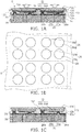
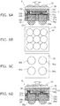
- FIG. 1A is a schematic cross-sectional view of a light emitting device according to a first embodiment of the invention
- FIG. 1B is a bottom view of the light emitting device in FIG. 1A .
- a multilayer body 12 has an upper layer 12a including a light emitting layer 12e, and a lower layer 12b, and has a first surface 12c which is exposed, and a second surface 12d on the opposite side.
- the upper layer 12a may include a p-type cladding layer, a light emitting layer 12e, and an n-type cladding layer.
- the lower layer 12b may be of n-type and serve as a lateral path of current.
- the conductivity type is not limited thereto, but may be the opposite conductivity type.
- a p-side electrode 14 provided on the surface of the upper layer 12a of the multilayer body 12 is connected to a p-side metal interconnect layer 24a through a p-side seed metal 22a. Furthermore, an n-side electrode 16 is connected to an n-side metal interconnect layer 24b through an n-side seed metal 22b.
- a dielectric film 20 made of an organic or inorganic material is filled between the seed metal 22a, 22b and the second surface 12d.
- a p-side metal pillar 26a and an n-side metal pillar 26b are provided on the p-side metal interconnect layer 24a and the n-side metal interconnect layer 24b, respectively, and surrounded by a (reinforcing) resin 28 so as to expose at least the surface of the metal pillars 26. Even if the multilayer body 12 is thin, its mechanical strength can be maintained by the metal pillars 26a, 26b and the reinforcing resin 28.
- the metal pillars 26 serve to reduce stress applied to the multilayer body 12 through mounting terminals.
- the metal interconnect layer 24a, 24b and the metal pillar 26a, 26b can be made of a material such as copper, gold, nickel, and silver. Among them, copper is more preferable, because it has good thermal conductivity, high migration resistance, and superior adhesion to the dielectric film. Although the following embodiments assume that the material of the metal interconnect layer 24 and the metal pillar 26 is copper, it is understood that the material is not limited to copper.
- the p-side seed metal 22a, the p-side copper interconnect layer 24a, and the p-side copper pillar 26a constitute a p-side extraction electrode which can be connected to the p-side electrode 14 provided in the multilayer body 12.
- n-side seed metal 22b, the n-side copper interconnect layer 24b, and the n-side copper pillar 26b constitute an n-side extraction electrode which can be connected to the n-side electrode 16 provided in the multilayer body 12.
- a diameter of the copper pillar 26 is larger than a diameter of an opening portion of the copper interconnect layer 24 in contact with the p-side electrode 14 or the n-side electrode 16.
- the shape may be other than a circle, and in that case, the area of the base of the copper pillar 26 is larger than the area of the opening portion of the copper interconnect layer 24 in contact with the p-side electrode 14 or the n-side electrode 16.
- light from the light emitting layer 12e can be emitted primarily from the first surface 12c of the multilayer body 12 in the upward direction of FIG. 1A .
- FIGS. 1A and 1B show a light emitting device based on WLP (wafer-level package). That is, one block indicated by the dashed line in FIG. 1B corresponds to an individual light emitting device.
- WLP wafer-level package
- Such wafer-level assembly facilitates implementing CSP (chip size package), where the light emitting device is downsized close to the bare chip size.
- CSP chip size package
- this embodiment can be referred to as a WLP light emitting device.
- FIG. 1C shows a light emitting device according to a first variation of the first embodiment.
- a separating portion 12f is provided in the multilayer body 12. In separation process into the individual light emitting device, the separation portion 12f facilitates avoiding cracking of GaN or other material, which is thin, hard, and brittle.
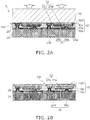
- FIG. 2A is a schematic cross-sectional view of a first example not forming part of the claimed invention and FIG. 2B is a schematic cross-sectional view of a second variation of the first embodiment.
- the multilayer body 12 is often crystal-grown on a sapphire or other translucent substrate 10, or crystal-grown on a GaAs or other provisional substrate and then transferred onto a translucent substrate 10 by a wafer bonding process or the like.
- FIG. 2A shows a WLP light emitting device with the translucent substrate 10 left behind.
- the substrate in the crystal growth process is often as thick as several hundred ⁇ m to reduce cracking and warpage.
- the translucent substrate 10 can be thinned by grinding, because the mechanical strength can be increased by the copper pillar 26 and the filling of the reinforcing resin 28.
- the second variation as shown in FIG. 2B uses a thick copper interconnect layer 24c, 24d as an extraction electrode without providing a copper pillar.
- the thick copper interconnect layer 24c functions as the p-side metal interconnect layer 24a in FIG. 2A .
- the thick copper interconnect layer 24d functions as the n-side metal interconnect layer 24b in FIG. 2A . This can simplify the structure and manufacturing process.
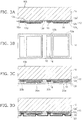
- FIGS. 3A to 3D show the process from the formation of a light emitting element to the film formation of a seed metal in the manufacturing method of the first embodiment.
- a multilayer body 12 having a lower layer 12b illustratively including a buffer layer and an n-type layer, and an upper layer 12a is formed on a first surface 10a of a translucent substrate 10 illustratively made of sapphire.
- the first surface 12c of the multilayer body 12 is adjacent to the first surface 10a of the translucent substrate 10.
- the second surface (dashed line) 12d of the multilayer body 12 includes the surface of the upper layer 12a and the surface of the lower layer 12b exposed by removal of the upper layer 12a, and thus has a step difference.
- the lower layer 12b is provided in an upward position as compared to the upper layer 12a.
- the upper or lower is called, if FIG. 3A is upside-down.
- the lower layer 12b is grown on the translucent substance 10, and the upper layer 12a is grown on the lower layer 12b.
- FIG. 3A shows the electrode pattern which is a plan view from a bottom side of FIG. 3A .
- a dielectric film 20 is formed so as to cover the p-side electrode 14 and the n-side electrode 16, and openings (first opening and second opening) 20a, 20b are formed so as to expose part of the p-side electrode 14 and the n-side electrode 16, respectively ( FIG. 3C ).
- a seed metal 22 illustratively made of Ti/Cu is formed by sputtering, for example ( FIG. 3D ).
- the n-side electrode 16 can be a multilayer of Ti/Al/Pt/Au
- the p-side electrode 14 can be a multilayer of Ni/Al (or Ag)/Au.
- sandwiching a high-reflection film illustratively made of Al or Ag facilitates reflecting upward the emission light from the light emitting layer 12e to extract a high optical output.
- a pad made of Au can be omitted.
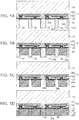
- FIGS. 4A to 4C are process cross-sectional views showing the process for forming copper interconnect layers in the manufacturing method of the first embodiment.
- a photoresist 40 is patterned on the seed metal 22 ( FIG. 4A ), and the patterned photoresist 40 is used as a mask to selectively form copper interconnect layers 24 by electrolytic plating.
- copper interconnect layers 24a, 24b separated from each other are formed ( FIG. 4B ).
- the copper interconnect layers 24a, 24b are formed so that the diameter or the area of the base of the copper interconnect layer 24a, 24b is larger than that of the openings 20a, 20b.
- the thin seed metal 22 serves as a current path in the electrolytic plating process.
- the photoresist 40 is removed illustratively by ashing, which results in the structure shown in FIG. 4C .
- FIGS. 5A to 5D show the process for forming a copper pillar and reinforcing resin in the manufacturing method of the first embodiment.
- a thick-film photoresist 42 is patterned to form an opening 42a on the p-side copper interconnect layer 24a and an opening 42b on the n-side copper interconnect layer 24b.
- a p-side copper pillar 26a connected to the p-side electrode 14 and an n-side copper pillar 26b connected to the n-side electrode 16 are formed by electrolytic plating ( FIG. 5B ).
- the thin seed metal 22 serves as a current path in the electrolytic plating process. If the thickness of the copper pillar 26 is in the range of e.g. 10 to several hundred ⁇ m, the strength of the light emitting device can be maintained even when the translucent substrate 10 is separated.
- the openings 42a, 42b may be formed in a dielectric film.
- the photoresist 42 is removed illustratively by ashing, and the exposed region of the seed metal 22 is removed illustratively by wet etching.
- the seed metal 22 is separated into a p-side seed metal 22a and an n-side seed metal 22b ( FIG. 5C ).
- a reinforcing resin 28 is formed around the copper pillar 26a, 26b to a thickness generally equal to or less than the thickness of the copper pillar 26a, 26b ( FIG. 5D ).
- the WLP light emitting device of FIG. 2A is obtained.
- the WLP light emitting device shown in FIG. 1A is obtained.
- the layer made of the resin and metal is flexible, and the metal is formed by plating at near room temperature.
- the residual stress occurring with respect to the translucent substrate 10 is relatively low.
- it is bonded to a silicon substrate with a metal layer formed thereon using Au-Sn solder at a high temperature of 300°C or more, and then the multilayer body 12 made of GaN is separated by laser irradiation.
- the translucent substrate and the silicon substrate being different in thermal expansion coefficient are both rigid, and are bonded together at high temperature. Hence, a high residual stress remains between these substrates.
- the device can be manufactured at high yield without trouble such as cracking in the multilayer body 12.
- this embodiment based on WLP can readily achieve a small light emitting device close to the chip size, which is typically several hundred ⁇ m to several mm for the multilayer body 12 made of nitride materials.
- Such a manufacturing method does not require mounting members such as a lead frame and ceramic substrate, and can perform the wiring process and sealing process at wafer level. Furthermore, inspection can be performed at wafer level. Hence, the productivity of the manufacturing process can be enhanced, which consequently facilitates cost reduction.
- FIG. 6A is a schematic cross-sectional view of an individual light emitting device according to a second embodiment of the invention
- FIG. 6B is a schematic top view
- FIG. 6C is a schematic bottom view of the light emitting device in FIG. 6A
- FIG. 6D is a schematic cross-sectional view of a variation of the second embodiment.
- solder ball 36a and a solder ball 36b are provided on the surface of the copper pillar 26a and the surface of the copper pillar 26b, respectively, in a BGA (ball grid array) configuration.
- the material of the solder ball 36 is not limited, but can be lead-free by using SnAg, for example.
- a phosphor layer 30 is provided to a illustratively uniform thickness on the first surface 12c of the multilayer body 12.
- the phosphor layer 30 can absorb emission light from the light emitting layer 12e and emit wavelength-converted light.
- mixed light of the emission light from the light emitting layer live and the wavelength-converted light can be emitted.
- the light emitting layer 12e is nitride-based, a white color, warm white color and the like can be obtained as a mixed color of the blue light, which is the emission light, and the yellow light, which is the wavelength-converted light from a yellow phosphor.
- a phosphor layer 30 having a substantially uniform thickness is provided near the light emitting layer 12e, and emission light is injected into the phosphor layer 30 before diverging. Hence, the spread of light of the emission light from the light emitting layer is made close to that of the wavelength-converted light, which facilitates reducing color unevenness.
- a convex lens 32 illustratively made of quartz glass can be further provided on the phosphor layer 30 to converge the mixed light of white or warm white color, for example, which facilitates achieving higher brightness. Furthermore, because the convex lens 32 is provided near the light emitting layer 12e without the intermediary of a sealing resin, the size of the lens can be decreased, which facilitates downsizing the device.
- WLP facilitates downsizing the light emitting device. Furthermore, because the convex lens 32 can be formed in the wafer state, an assembly process with high productivity can be realized, which facilitates cost reduction.
- the solder ball 36 provided on the surface of the copper pillar 26 facilitates installation on the mounting substrate.
- a concave lens 33 is provided instead of the convex lens 32 so that the emission light can diverge.
- the emission light needs to be incident on the side surface of a light guide plate so as to spread along the surface of the light guide plate.
- the concave lens 33 is suitable for this case.
- FIGS. 7A to 7E are process cross-sectional views of a method for manufacturing a light emitting device according to the second embodiment.
- FIG. 7A shows a light emitting device (WLP) 5 from which the translucent substrate 10 is removed.
- WLP light emitting device
- a phosphor layer 30 is formed on the first surface 12c of the multilayer body 12 which is exposed.
- the phosphor layer 30 can be formed to a thickness in the range from several to several hundred ⁇ m illustratively by a sputtering method, an ink-jet method, a method of applying a silicone resin mixed with phosphor particles, and a method of applying a liquid glass mixed with phosphor particles ( FIG. 7B ).
- a convex lens 32 is formed from quartz glass, for example ( FIG. 7C ), and a solder ball 36 is formed on the surface of the copper pillar 26 ( FIG. 7D ).
- dicing is used for separation ( FIG. 7E ), which is easy because the translucent substrate 10 is removed.
- cutting can be performed by a method such as mechanical cutting using a diamond blade or the like, cutting by laser irradiation, and cutting by high-pressure water.
- FIGS. 8A to 8C are process cross-sectional views of a manufacturing method of a first variation of the second embodiment.
- the lower layer 12b of the multilayer body 12 is continuous along the first surface 10a of the translucent substrate 10. This is because the multilayer body 12 made of GaN is separated by laser irradiation more easily if the multilayer body 12 is formed entirely on the wafer.
- the wafer including the multilayer body 12 is desirably fixed onto a flat tool or jig by vacuum suction, adhesion or the like.
- the portion of the multilayer body 12 between the light emitting elements is removed illustratively by further laser irradiation while the wafer including the multilayer body 12 is fixed ( FIG. 8A ). Furthermore, a phosphor layer 30, a convex lens 32, and a solder ball 36 are formed ( FIG. 8B ), followed by separation ( FIG. 8C ).
- the wafer including the multilayer body 12 may be fixed to a jig which can be detached from the laser irradiation apparatus, and the multilayer body 12 may be separated by a combination of photolithography and etching.
- the multilayer body 12 which is rigid and thin, is separated into small size, the risk of cracking in the multilayer body 12 in the subsequent handling of the wafer is significantly reduced. Furthermore, also after separation, because the multilayer body 12 is separated into small size, the multilayer body 12 is resistant to cracking. Moreover, the package is flexible as a whole, which results in enhancing the reliability of connection points after mounting. Furthermore, the package has small warpage, which facilitates mounting. Moreover, it can also be mounted on an object having a curved surface.
- FIGS. 9A to 9F are process cross-sectional views showing an example method for forming a lens.
- a lens material made of quartz glass 60, plastic or the like is formed on the support 62 such as a semiconductor multilayer body and phosphor layer, and a dot pattern of a mask material such as a photoresist 50 is formed on the lens material ( FIG. 9A ).
- Processing with low selective ratio for the resist is performed stepwise such as the first step ( FIG. 9B ), second step ( FIG. 9C ), and third step ( FIG. 9D ). In each step, the portion around the photoresist 50 is sloped while the resist dot pattern is reduced by etching.
- the cross section has a steeper slope downward ( FIG. 9E ).
- mirror finishing by isotropic etching using CDE (chemical dry etching) or wet etching is performed to smooth the surface, and the lens is completed ( FIG. 9F ).
- CDE chemical dry etching
- wet etching is performed to smooth the surface, and the lens is completed ( FIG. 9F ).
- a convex or concave lens can be formed on the light emitting device.
- FIGS. 10A to 10C are process cross-sectional views showing another example method for forming a lens.
- FIGS. 10A to 10C it is also possible to use a imprint process.
- FIGS. 11A to 11D are process cross-sectional views of a manufacturing method of a second variation of the second embodiment.
- a convex lens 32 is first formed on the first surface 12c of the multilayer body 12 ( FIG. 11A ), and then a phosphor layer 31 is formed on the convex lens 32 ( FIG. 11B ). Subsequently, a solder ball 36 is formed on the surface of the copper pillar 26 ( FIG. 11C ), and an individual light emitting device 6 is obtained by separation ( FIG. 11D ).
- the substrate of the WLP-based light emitting device is removed.
- a light emitting device having lower profile is provided.
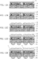
- FIGS. 12A to 12E are process cross-sectional views of a method for manufacturing a light emitting device according to a second example not forming part of the claimed invention.
- the thickness of the translucent substrate 10 can be reduced by grinding. For example, leaving as much as several ten ⁇ m ( FIG. 12A ) facilitates enhancing the mechanical strength as compared with the structure in which the translucent substrate 10 is entirely removed. Subsequently, the processes of forming a phosphor layer 30 ( FIG. 12B ), forming a convex lens 32 ( FIG. 12C ), forming a solder ball 36 ( FIG. 12D ), and separation ( FIG. 12E ) are performed.
- FIGS. 13A to 13D are process cross-sectional views of a manufacturing method of a variation of the second example not forming part of the claimed invention.
- Forming a convex lens 32 as shown in FIG. 13A is followed by forming a phosphor layer 31 ( FIG. 13B ), forming a solder ball 36 ( FIG. 13C ), and separating ( FIG. 13D ).
- thinning and leaving the translucent substrate 10 facilitates enhancing the mechanical strength while keeping small thickness.
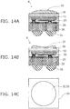
- FIG. 14A is a schematic cross-sectional view of a light emitting device not forming part of the claimed invention having a convex lens
- FIG. 14B is a schematic cross-sectional view of a light emitting not forming part of the claimed invention having a concave lens
- FIG. 14C is a top view of the light emitting device of FIGS. 14A and 14B .
- the lens in the first and second embodiments and the first and second examples is an array lens, However, it is also possible to use a single lens as shown in the examples not forming part of the claimed invention in FIG. 14A or 14B . Use of a single lens can simplify the optical design and manufacturing process.
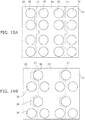
- FIGS. 15A to 15C are schematic views of variations of the lens.
- lenses 32a, 32b, 32c, 32d, 32e having different sizes may be arranged.
- the area covered with lenses can be increased by placing small lenses in a gap between large lenses.
- a lens 33a having a rectangular outline may be used.
- FIG. 16A is a schematic cross-sectional view of a light emitting device according to a third example not forming part of the claimed invention, and FIG. 16B is a bottom view thereof.
- adjacent multilayer bodies are spaced from each other. Patterning is performed so that the first p-side electrode 14 of the first multilayer body is connected to the second n-side electrode 16 of the second multilayer body adjacent thereto. Furthermore, the seed metal 22 between the first multilayer body and the second multilayer body may be left unremoved. Thus, the seed metal 22 and the copper interconnect layer 24 are connected between the first and second light emitting elements. That is, the two light emitting elements can be connected in series. Such series connection facilitates achieving higher output. It is understood that the number of series connection is not limited to two, but series connection with more stages is possible. Furthermore, multilayer bodies adjacent in the direction crossing the juxtaposing direction of the first and second multilayer bodies can be connected to each other to provide parallel connection.
- the seed metal 22 and the copper interconnect layer 24 are connected among 2x2 light emitting elements.
- the 2x2 light emitting elements do not necessarily need to be separated on the outside thereof. If this configuration continues throughout the wafer, light emitting elements can be cut out in arbitrary units.
- FIGS. 17A to 17E , and 18A and 18B are process cross-sectional views of a manufacturing method of a variation of the third example not forming part of the claimed invention.
- the translucent substrate 10 may be separated for each light emitting element. This can realize a reliable structure because the individual light emitting element is protected by the rigid translucent substrate 10. Furthermore, in the manufacturing method therefor, as shown in FIG. 17A , a groove 10c can be formed in the gap of the translucent substrate 10 between the light emitting elements from the light emitting element formation surface 10a side.
- the groove 10c can be formed illustratively before or after the step of forming the light emitting element, and can be based on a method such as etching, laser processing, and blade cutting. Then, because the rigid translucent substrate 10 is separated into small size when the translucent substrate 10 is thinly ground later ( FIG. 17E ), the cracking can be significantly reduced.
- the portion free from the rigid translucent substrate is cut ( FIG. 18B )
- high productivity and yield can be achieved.
- the translucent substrate 10 and the multilayer body 12 are separated into small size, the translucent substrate 10 and the multilayer body 12 are resistant to cracking.
- the package is flexible as a whole, which results in enhancing the reliability of connection points after mounting.
- the package has small warpage, which facilitates mounting.
- it can also be mounted on an object having a curved surface.
- FIGS. 19A and 19B are schematic views showing a variation of the pattern of the copper interconnect layer.
- the separating region 21 between the p-side electrode 14 and the n-side electrode 16 is linear. Hence, the wafer may crack in the separating region 21.
- the protruding portion of the copper interconnect layer 24 serves for reinforcement, which facilitates maintaining the mechanical strength even if the translucent substrate 10 is thinned by grinding.
- the copper pillars 26 are arranged in a generally lattice-like configuration. However, it is also possible to use an arrangement as shown in FIG. 19B . It is understood that the same effect is achieved also in the configuration where the translucent substrate 10 is separated.
- FIG. 20A is a schematic plan view of a basic electrode pattern for two light emitting element chips
- FIGS. 20B to 20D are schematic plan views of its variations.
- Light emission occurs in the region where the current flows in the vertical direction of the chip.
- a high optical output can be achieved by increasing the area of the upper layer 12a including the light emitting layer 12e.
- the area of the lower layer 12b exposed by removal of the upper layer 12a is an n-type non-emitting region, and low contact resistance to the n-side electrode 16 is readily achieved even if the area is small.
- the copper interconnect layer 24 can be used for connection to a wider extraction electrode. If the area of the extraction electrode connected to the p-side electrode 14 is generally equal to the size of the extraction electrode connected to the n-side electrode 16, the device can be mounted on the substrate through the solder ball 36 in a balanced manner.
- the upper layer 12a including the light emitting layer 12e is placed at the center, and the n-type lower layer 12b is placed therearound. This can shorten the current supply path. Furthermore, because the light emitting region is located at the center, it can be readily aligned with the optical axis of the lens.
- the lower layer 12b is exposed at lattice-like positions where the n-side electrode 16 is provided, and the p-side electrode 14 is provided therearound. This can further shorten the current path.
- the p-side electrode 14 is placed at the center, and the n-side electrode 16 is placed at four corners therearound. This can further increase the light emitting region. Furthermore, because the light emitting region is located at the center, it can be readily aligned with the optical axis of the lens.
- the first to fourth embodiments and the variations thereof can provide light emitting devices downsized close to the bare chip size. These light emitting devices can be widely used in, for example, illumination devices, display devices, and backlight sources for image display devices.
- the assembly and inspection process can be performed at wafer level, which facilitates achieving high productivity. Hence, cost reduction can be achieved.
Description
- Light emitting devices capable of emitting visible and white light are expanding their applications to, for example, illumination devices, display devices, and backlight sources for image display devices.
- In these applications, there is a growing demand for downsizing. In this context, downsizing of electronic devices has been facilitated by an SMD (surface-mounted device) light emitting device in which a light emitting element chip is bonded onto a lead frame and resin-molded.
- To replace fluorescent lamps and incandescent bulbs by illumination devices based on semiconductor light emitting devices having low power loss, it is necessary to enhance mass productivity and reduce cost.
-
JP-A-2006-128625 - However, this example needs the interconnect layer and the columnar electrode for bonding the light emitting element chip onto the transparent substrate with high positional accuracy, and is insufficient to meet the requirements for downsizing and mass productivity.
-
US 6,331,450 B1 relates to a flip-chip-type device which comprises a positive electrode and a negative electrode, which are both provided on the same side of the device. As shown in e.g. Fig. 2c of the document, metal pillars 220 are directly connected to electrodes 120 and 140. -
EP 0 704 899 A2 relates to problems that arise when connecting a semiconductor chip to a carrier film via an adhesive film. In particular, positioning the adhesive film relative to the semiconductor chip is described as being problematic. Also, the formation of small through holes in an organic insulating film disposed on the carrier film is described as being difficult. These problems are addressed by forming the adhesive layer before cutting the semiconductor chips and forming the through holes of the carrier film by AR laser processing and washing processing. -
US 6,121,689 relates to the flip-chip attachment of a chip to a substrate and problems that arise in this regard when underfilling the volume between the chip and the substrate with an underfill encapsulant material. Four problems are mentioned, including the amount of time required to complete the underfilling and the reduced reliablitiy of the underfill process when increasing the size of the chip. According to a described embodiment, in order to solve these problems, the circuitry on the bottom surface of a chip is coated with an encapsulant before connecting the chip to the substrate. -
US 2007/262338 A1 relates to an LED chip with a structure in which an n-type semiconductor layer and a p-type semiconductor layer are successively formed on the lower face of an element substrate, with the p-type semiconductor layer being formed on an area except for an area for an n-electrode. - Document
JP 2008 277409 A - Document
US 2007/262338 A1 relates to a flip chip LED having a particular configuration of electrodes. - Document
US 2009/179207 A1 relates a flip chip LED is mounted on a submount wafer and a growth substrate is subsequently removed. - The present invention is defined by the appended independent claims. Advantageous embodiments are described in the appended dependent claims.
-
-
FIGS. 1A to 1C are schematic views of a light emitting device according to a first embodiment; -
FIG. 2A is a schematic cross-sectional view of a first example not forming part of the claimed invention andFIG. 2B is a cross-sectional view of a variation of the first embodiment; -
FIGS. 3A to 3D are process cross-sectional views of a light emitting device according to the first embodiment; -
FIGS. 4A to 4C are process cross-sectional views of a light emitting device according to the first embodiment; -
FIGS. 5A to 5D are process cross-sectional views of a light emitting device according to the first embodiment; -
FIGS. 6A to 6D are schematic views of a light emitting device according to a second embodiment; -
FIGS. 7A to 7E are process cross-sectional views of a light emitting device according to the second embodiment; -
FIGS. 8A to 8C are process cross-sectional views of a manufacturing method of a first variation of the second embodiment; -
FIGS. 9A to 9F are process cross-sectional views showing a method for forming a lens; -
FIGS. 10A to 10C are process cross-sectional views showing another example method for forming a lens; -
FIGS. 11A to 11D are process cross-sectional views of a manufacturing method of a second variation of the second embodiment; -
FIGS. 12A to 12E are process cross-sectional views of a method for manufacturing a light emitting device according to a second example not forming part of the claimed invention; -
FIGS. 13A to 13D are process cross-sectional views of a manufacturing method of a variation of the second example not forming part of the claimed invention; -
FIGS. 14A to 14C are schematic views of a light emitting device according to a second example not forming part of the claimed invention having a convex lens or a concave lens; -
FIGS. 15A to 15C are schematic views of variations of a lens; -
FIGS. 16A and 16B are schematic views of a light emitting device according to a third example not forming part of the claimed invention; -
FIGS. 17A to 17E are process cross-sectional views of a manufacturing method of a variation of the third example not forming part of the claimed invention; -
FIGS. 18A and 18B are process cross-sectional views of a manufacturing method of a variation of the third example not forming part of the claimed invention; -
FIGS. 19A and 19B are schematic views showing variations of the pattern of a metal interconnect layer; and -
FIGS. 20A to 20D are schematic plan views showing variations of an electrode pattern. - Embodiments of the invention will now be described with reference to the drawings.
-
FIG. 1A is a schematic cross-sectional view of a light emitting device according to a first embodiment of the invention, andFIG. 1B is a bottom view of the light emitting device inFIG. 1A . - In
FIGS. 1A and 1B , amultilayer body 12 has anupper layer 12a including alight emitting layer 12e, and alower layer 12b, and has afirst surface 12c which is exposed, and asecond surface 12d on the opposite side. Theupper layer 12a may include a p-type cladding layer, alight emitting layer 12e, and an n-type cladding layer. Thelower layer 12b may be of n-type and serve as a lateral path of current. However, the conductivity type is not limited thereto, but may be the opposite conductivity type. - A p-
side electrode 14 provided on the surface of theupper layer 12a of themultilayer body 12 is connected to a p-sidemetal interconnect layer 24a through a p-side seed metal 22a. Furthermore, an n-side electrode 16 is connected to an n-sidemetal interconnect layer 24b through an n-side seed metal 22b. Adielectric film 20 made of an organic or inorganic material is filled between theseed metal second surface 12d. - A p-
side metal pillar 26a and an n-side metal pillar 26b are provided on the p-sidemetal interconnect layer 24a and the n-sidemetal interconnect layer 24b, respectively, and surrounded by a (reinforcing)resin 28 so as to expose at least the surface of themetal pillars 26. Even if themultilayer body 12 is thin, its mechanical strength can be maintained by themetal pillars resin 28. Themetal pillars 26 serve to reduce stress applied to themultilayer body 12 through mounting terminals. - The
metal interconnect layer metal pillar metal interconnect layer 24 and themetal pillar 26 is copper, it is understood that the material is not limited to copper. - The p-
side seed metal 22a, the p-sidecopper interconnect layer 24a, and the p-side copper pillar 26a constitute a p-side extraction electrode which can be connected to the p-side electrode 14 provided in themultilayer body 12. - Furthermore, the n-
side seed metal 22b, the n-sidecopper interconnect layer 24b, and the n-side copper pillar 26b constitute an n-side extraction electrode which can be connected to the n-side electrode 16 provided in themultilayer body 12. - In
FIGS. 1A and 1B , a diameter of thecopper pillar 26 is larger than a diameter of an opening portion of thecopper interconnect layer 24 in contact with the p-side electrode 14 or the n-side electrode 16. Here, the shape may be other than a circle, and in that case, the area of the base of thecopper pillar 26 is larger than the area of the opening portion of thecopper interconnect layer 24 in contact with the p-side electrode 14 or the n-side electrode 16. - As indicated by the block arrow, light from the
light emitting layer 12e can be emitted primarily from thefirst surface 12c of themultilayer body 12 in the upward direction ofFIG. 1A . -
FIGS. 1A and 1B show a light emitting device based on WLP (wafer-level package). That is, one block indicated by the dashed line inFIG. 1B corresponds to an individual light emitting device. Such wafer-level assembly facilitates implementing CSP (chip size package), where the light emitting device is downsized close to the bare chip size. Furthermore, it may be possible that there is no need to provide a sealing resin, which facilitates achieving lower profile. Thus, this embodiment can be referred to as a WLP light emitting device. -
FIG. 1C shows a light emitting device according to a first variation of the first embodiment. - A separating
portion 12f is provided in themultilayer body 12. In separation process into the individual light emitting device, theseparation portion 12f facilitates avoiding cracking of GaN or other material, which is thin, hard, and brittle. -
FIG. 2A is a schematic cross-sectional view of a first example not forming part of the claimed invention andFIG. 2B is a schematic cross-sectional view of a second variation of the first embodiment. - In the first example as shown in
FIG. 2A , in the case
where thelight emitting layer 12e is made of a nitride semiconductor, themultilayer body 12 is often crystal-grown on a sapphire or othertranslucent substrate 10, or crystal-grown on a GaAs or other provisional substrate and then transferred onto atranslucent substrate 10 by a wafer bonding process or the like.FIG. 2A shows a WLP light emitting device with thetranslucent substrate 10 left behind. The substrate in the crystal growth process is often as thick as several hundred µm to reduce cracking and warpage. In this example, the
translucent substrate 10 can be thinned by grinding, because the mechanical strength can be increased by thecopper pillar 26 and the filling of the reinforcingresin 28. - The second variation as shown in
FIG. 2B uses a thick
copper interconnect layer copper interconnect layer 24c functions as the p-sidemetal interconnect layer 24a inFIG. 2A . The thickcopper interconnect layer 24d functions as the n-sidemetal interconnect layer 24b inFIG. 2A . This can simplify the structure and manufacturing process. -
FIGS. 3A to 3D show the process from the formation of a light emitting element to the film formation of a seed metal in the manufacturing method of the first embodiment. - As shown in
FIG. 3A , amultilayer body 12 having alower layer 12b illustratively including a buffer layer and an n-type layer, and anupper layer 12a, is formed on afirst surface 10a of atranslucent substrate 10 illustratively made of sapphire. Thefirst surface 12c of themultilayer body 12 is adjacent to thefirst surface 10a of thetranslucent substrate 10. The second surface (dashed line) 12d of themultilayer body 12 includes the surface of theupper layer 12a and the surface of thelower layer 12b exposed by removal of theupper layer 12a, and thus has a step difference. Thelower layer 12b is provided in an upward position as compared to theupper layer 12a. The upper or lower is called, ifFIG. 3A is upside-down. Generally, thelower layer 12b is grown on thetranslucent substance 10, and theupper layer 12a is grown on thelower layer 12b. - A p-
side electrode 14 is formed on the surface of theupper layer 12a, and an n-side electrode 16 is formed on the surface of thelower layer 12b. The result is as shown inFIG. 3A. FIG. 3B shows the electrode pattern which is a plan view from a bottom side ofFIG. 3A . Adielectric film 20 is formed so as to cover the p-side electrode 14 and the n-side electrode 16, and openings (first opening and second opening) 20a, 20b are formed so as to expose part of the p-side electrode 14 and the n-side electrode 16, respectively (FIG. 3C ). Furthermore, aseed metal 22 illustratively made of Ti/Cu is formed by sputtering, for example (FIG. 3D ). - Here, for example, the n-
side electrode 16 can be a multilayer of Ti/Al/Pt/Au, and the p-side electrode 14 can be a multilayer of Ni/Al (or Ag)/Au. In the p-side electrode 14, sandwiching a high-reflection film illustratively made of Al or Ag facilitates reflecting upward the emission light from thelight emitting layer 12e to extract a high optical output. Furthermore, because theseed metal 22 is provided, a pad made of Au can be omitted. -
FIGS. 4A to 4C are process cross-sectional views showing the process for forming copper interconnect layers in the manufacturing method of the first embodiment. - For example, a
photoresist 40 is patterned on the seed metal 22 (FIG. 4A ), and the patternedphotoresist 40 is used as a mask to selectively form copper interconnect layers 24 by electrolytic plating. Thus,copper interconnect layers FIG. 4B ). Preferably, thecopper interconnect layers copper interconnect layer openings thin seed metal 22 serves as a current path in the electrolytic plating process. Subsequently, thephotoresist 40 is removed illustratively by ashing, which results in the structure shown inFIG. 4C . -
FIGS. 5A to 5D show the process for forming a copper pillar and reinforcing resin in the manufacturing method of the first embodiment. - As shown in
FIG. 5A , a thick-film photoresist 42 is patterned to form anopening 42a on the p-sidecopper interconnect layer 24a and an opening 42b on the n-sidecopper interconnect layer 24b. Subsequently, a p-side copper pillar 26a connected to the p-side electrode 14 and an n-side copper pillar 26b connected to the n-side electrode 16 are formed by electrolytic plating (FIG. 5B ). Here again, thethin seed metal 22 serves as a current path in the electrolytic plating process. If the thickness of thecopper pillar 26 is in the range of e.g. 10 to several hundred µm, the strength of the light emitting device can be maintained even when thetranslucent substrate 10 is separated. Here, alternatively, theopenings 42a, 42b may be formed in a dielectric film. - Then, the
photoresist 42 is removed illustratively by ashing, and the exposed region of theseed metal 22 is removed illustratively by wet etching. Thus, theseed metal 22 is separated into a p-side seed metal 22a and an n-side seed metal 22b (FIG. 5C ). - Subsequently, a reinforcing
resin 28 is formed around thecopper pillar copper pillar FIG. 5D ). Thus, the WLP light emitting device ofFIG. 2A is obtained. Furthermore, by removing thetranslucent substrate 10, the WLP light emitting device shown inFIG. 1A is obtained. - Here, the layer made of the resin and metal is flexible, and the metal is formed by plating at near room temperature. Hence, the residual stress occurring with respect to the
translucent substrate 10 is relatively low. In the conventional technique for separating themultilayer body 12 from thetranslucent substrate 10 at wafer level, for example, it is bonded to a silicon substrate with a metal layer formed thereon using Au-Sn solder at a high temperature of 300°C or more, and then themultilayer body 12 made of GaN is separated by laser irradiation. However, in this conventional technique, the translucent substrate and the silicon substrate being different in thermal expansion coefficient are both rigid, and are bonded together at high temperature. Hence, a high residual stress remains between these substrates. Consequently, when the separation is started by laser irradiation, the residual stress is locally relieved from the separated portion and unfortunately causes cracks in the thin,brittle multilayer body 12. In contrast, in this embodiment, the residual stress is low, and themultilayer body 12 is separated in the state of being fixed to a flexible support. Hence, the device can be manufactured at high yield without trouble such as cracking in themultilayer body 12. - Furthermore, this embodiment based on WLP can readily achieve a small light emitting device close to the chip size, which is typically several hundred µm to several mm for the
multilayer body 12 made of nitride materials. - Such a manufacturing method does not require mounting members such as a lead frame and ceramic substrate, and can perform the wiring process and sealing process at wafer level. Furthermore, inspection can be performed at wafer level. Hence, the productivity of the manufacturing process can be enhanced, which consequently facilitates cost reduction.
-
FIG. 6A is a schematic cross-sectional view of an individual light emitting device according to a second embodiment of the invention,FIG. 6B is a schematic top view,FIG. 6C is a schematic bottom view of the light emitting device inFIG. 6A, and FIG. 6D is a schematic cross-sectional view of a variation of the second embodiment. - In addition to the structure of the first embodiment shown in
FIG. 1A , asolder ball 36a and asolder ball 36b are provided on the surface of thecopper pillar 26a and the surface of thecopper pillar 26b, respectively, in a BGA (ball grid array) configuration. The material of thesolder ball 36 is not limited, but can be lead-free by using SnAg, for example. - On the other hand, a
phosphor layer 30 is provided to a illustratively uniform thickness on thefirst surface 12c of themultilayer body 12. Thephosphor layer 30 can absorb emission light from thelight emitting layer 12e and emit wavelength-converted light. Thus, mixed light of the emission light from the light emitting layer live and the wavelength-converted light can be emitted. If thelight emitting layer 12e is nitride-based, a white color, warm white color and the like can be obtained as a mixed color of the blue light, which is the emission light, and the yellow light, which is the wavelength-converted light from a yellow phosphor. - In this embodiment, a
phosphor layer 30 having a substantially uniform thickness is provided near thelight emitting layer 12e, and emission light is injected into thephosphor layer 30 before diverging. Hence, the spread of light of the emission light from the light emitting layer is made close to that of the wavelength-converted light, which facilitates reducing color unevenness. - Furthermore, as shown in
FIG. 6A , aconvex lens 32 illustratively made of quartz glass can be further provided on thephosphor layer 30 to converge the mixed light of white or warm white color, for example, which facilitates achieving higher brightness. Furthermore, because theconvex lens 32 is provided near thelight emitting layer 12e without the intermediary of a sealing resin, the size of the lens can be decreased, which facilitates downsizing the device. - Thus, WLP facilitates downsizing the light emitting device. Furthermore, because the
convex lens 32 can be formed in the wafer state, an assembly process with high productivity can be realized, which facilitates cost reduction. In this embodiment, thesolder ball 36 provided on the surface of thecopper pillar 26 facilitates installation on the mounting substrate. - In the variation shown in
FIG. 6D , aconcave lens 33 is provided instead of theconvex lens 32 so that the emission light can diverge. For example, for use as a backlight source and the like, the emission light needs to be incident on the side surface of a light guide plate so as to spread along the surface of the light guide plate. Theconcave lens 33 is suitable for this case. -
FIGS. 7A to 7E are process cross-sectional views of a method for manufacturing a light emitting device according to the second embodiment. -
FIG. 7A shows a light emitting device (WLP) 5 from which thetranslucent substrate 10 is removed. - A
phosphor layer 30 is formed on thefirst surface 12c of themultilayer body 12 which is exposed. Thephosphor layer 30 can be formed to a thickness in the range from several to several hundred µm illustratively by a sputtering method, an ink-jet method, a method of applying a silicone resin mixed with phosphor particles, and a method of applying a liquid glass mixed with phosphor particles (FIG. 7B ). Subsequently, aconvex lens 32 is formed from quartz glass, for example (FIG. 7C ), and asolder ball 36 is formed on the surface of the copper pillar 26 (FIG. 7D ). Thus, a WLP-based light emitting device is completed. Furthermore, dicing is used for separation (FIG. 7E ), which is easy because thetranslucent substrate 10 is removed. Here, cutting can be performed by a method such as mechanical cutting using a diamond blade or the like, cutting by laser irradiation, and cutting by high-pressure water. -
FIGS. 8A to 8C are process cross-sectional views of a manufacturing method of a first variation of the second embodiment. - In the process cross-sectional views of
FIGS. 7A to 7E , thelower layer 12b of themultilayer body 12 is continuous along thefirst surface 10a of thetranslucent substrate 10. This is because themultilayer body 12 made of GaN is separated by laser irradiation more easily if themultilayer body 12 is formed entirely on the wafer. In this case, the wafer including themultilayer body 12 is desirably fixed onto a flat tool or jig by vacuum suction, adhesion or the like. - On the other hand, in the first variation, after the
translucent substrate 10 is separated, the portion of themultilayer body 12 between the light emitting elements is removed illustratively by further laser irradiation while the wafer including themultilayer body 12 is fixed (FIG. 8A ). Furthermore, aphosphor layer 30, aconvex lens 32, and asolder ball 36 are formed (FIG. 8B ), followed by separation (FIG. 8C ). Alternatively, the wafer including themultilayer body 12 may be fixed to a jig which can be detached from the laser irradiation apparatus, and themultilayer body 12 may be separated by a combination of photolithography and etching. Because themultilayer body 12, which is rigid and thin, is separated into small size, the risk of cracking in themultilayer body 12 in the subsequent handling of the wafer is significantly reduced. Furthermore, also after separation, because themultilayer body 12 is separated into small size, themultilayer body 12 is resistant to cracking. Moreover, the package is flexible as a whole, which results in enhancing the reliability of connection points after mounting. Furthermore, the package has small warpage, which facilitates mounting. Moreover, it can also be mounted on an object having a curved surface. -
FIGS. 9A to 9F are process cross-sectional views showing an example method for forming a lens. - A lens material made of
quartz glass 60, plastic or the like is formed on thesupport 62 such as a semiconductor multilayer body and phosphor layer, and a dot pattern of a mask material such as aphotoresist 50 is formed on the lens material (FIG. 9A ). Processing with low selective ratio for the resist is performed stepwise such as the first step (FIG. 9B ), second step (FIG. 9C ), and third step (FIG. 9D ). In each step, the portion around thephotoresist 50 is sloped while the resist dot pattern is reduced by etching. - Hence, after the resist is stripped off, the cross section has a steeper slope downward (
FIG. 9E ). Then, mirror finishing by isotropic etching using CDE (chemical dry etching) or wet etching is performed to smooth the surface, and the lens is completed (FIG. 9F ). Thus, a convex or concave lens can be formed on the light emitting device. -
FIGS. 10A to 10C are process cross-sectional views showing another example method for forming a lens. - As shown in
FIGS. 10A to 10C , it is also possible to use a imprint process. An SOG (spin on glass) 61 or the like, which is liquid and heat-vitrifiable, is applied onto thesupport 62 illustratively by spincoating (FIG. 10A ), and a mold such as astamper 53, which is patterned like a lens, is pressed thereto to form a lens shape (FIG. 10B ). Then, thestamper 53 is stripped off, and theSOG 61 is vitrified by heating (FIG. 10C ). In this process, the shape of thestamper 53 can be arbitrarily designed, and hence a lens having any shape can be readily manufactured. -
FIGS. 11A to 11D are process cross-sectional views of a manufacturing method of a second variation of the second embodiment. - In this variation, a
convex lens 32 is first formed on thefirst surface 12c of the multilayer body 12 (FIG. 11A ), and then aphosphor layer 31 is formed on the convex lens 32 (FIG. 11B ). Subsequently, asolder ball 36 is formed on the surface of the copper pillar 26 (FIG. 11C ), and an individuallight emitting device 6 is obtained by separation (FIG. 11D ). - In the individual
light emitting device 6 of the second embodiment and the variations associated therewith, the substrate of the WLP-based light emitting device is removed. Thus, a light emitting device having lower profile is provided. -
FIGS. 12A to 12E are process cross-sectional views of a method for manufacturing a light emitting device according to a second example not forming part of the claimed invention. - In the first example not forming part of the claimed invention shown in
FIG. 2A , the thickness of thetranslucent substrate 10 can be reduced by grinding. For example, leaving as much as several ten µm (FIG. 12A ) facilitates enhancing the mechanical strength as compared with the structure in which thetranslucent substrate 10 is entirely removed. Subsequently, the processes of forming a phosphor layer 30 (FIG. 12B ), forming a convex lens 32 (FIG. 12C ), forming a solder ball 36 (FIG. 12D ), and separation (FIG. 12E ) are performed. -
FIGS. 13A to 13D are process cross-sectional views of a manufacturing method of a variation of the second example not forming part of the claimed invention. - Forming a
convex lens 32 as shown inFIG. 13A is followed by forming a phosphor layer 31 (FIG. 13B ), forming a solder ball 36 (FIG. 13C ), and separating (FIG. 13D ). - In the light emitting device of the second example not forming part of the claimed invention and its variation, thinning and leaving the
translucent substrate 10 facilitates enhancing the mechanical strength while keeping small thickness. -
FIG. 14A is a schematic cross-sectional view of a light emitting device not forming part of the claimed invention having a convex lens,FIG. 14B is a schematic cross-sectional view of a light emitting not forming part of the claimed invention having a concave
lens, andFIG. 14C is a top view of the light emitting device ofFIGS. 14A and 14B . - The lens in the first and second embodiments and the first and second examples is an array lens, However, it is also
possible to use a single lens as shown in the examples not forming part of the claimed invention inFIG. 14A or 14B . Use of a single lens can simplify the optical design and manufacturing process. -
FIGS. 15A to 15C are schematic views of variations of the lens. - As shown in the plan views of
FIGS. 15A and 15B ,lenses FIG. 15C , alens 33a having a rectangular outline may be used. -
FIG. 16A is a schematic cross-sectional view of a light emitting device according to a third example not forming part of the claimed invention, andFIG. 16B is a bottom view thereof. - In this example, adjacent multilayer bodies are
spaced from each other. Patterning is performed so that the first p-side electrode 14 of the first multilayer body is connected to the second n-side electrode 16 of the second multilayer body adjacent thereto. Furthermore, theseed metal 22 between the first multilayer body and the second multilayer body may be left unremoved. Thus, theseed metal 22 and thecopper interconnect layer 24 are connected between the first and second light emitting elements. That is, the two light emitting elements can be connected in series. Such series connection facilitates achieving higher output. It is understood that the number of series connection is not limited to two, but series connection with more stages is possible. Furthermore, multilayer bodies adjacent in the direction crossing the juxtaposing direction of the first and second multilayer bodies can be connected to each other to provide parallel connection. - In
FIGS. 16A and 16B , theseed metal 22 and thecopper interconnect layer 24 are connected among 2x2 light emitting elements. However, the 2x2 light emitting elements do not necessarily need to be separated on the outside thereof. If this configuration continues throughout the wafer, light emitting elements can be cut out in arbitrary units. -
FIGS. 17A to 17E , and18A and 18B are process cross-sectional views of a manufacturing method of a variation of the third example not forming part of the claimed invention. - The
translucent substrate 10 may be separated for each light emitting element. This can realize a reliable structure because the individual light emitting element is protected by the rigidtranslucent substrate 10. Furthermore, in the manufacturing method therefor, as shown inFIG. 17A , agroove 10c can be formed in the gap of thetranslucent substrate 10 between the light emitting elements from the light emittingelement formation surface 10a side. Thegroove 10c can be formed illustratively before or after the step of forming the light emitting element, and can be based on a method such as etching, laser processing, and blade cutting. Then, because the rigidtranslucent substrate 10 is separated into small size when thetranslucent substrate 10 is thinly ground later (FIG. 17E ), the cracking can be significantly reduced. In addition, also in separation into packages, because the portion free from the rigid translucent substrate is cut (FIG. 18B ), high productivity and yield can be achieved. Furthermore, also after separation, because thetranslucent substrate 10 and themultilayer body 12 are separated into small size, thetranslucent substrate 10 and themultilayer body 12 are resistant to cracking. Moreover, the package is flexible as a whole, which results in enhancing the reliability of connection points after mounting. Furthermore, the package has small warpage, which facilitates mounting. Moreover, it can also be mounted on an object having a curved surface. -
FIGS. 19A and 19B are schematic views showing a variation of the pattern of the copper interconnect layer. - In
FIG. 16B , the separatingregion 21 between the p-side electrode 14 and the n-side electrode 16 is linear. Hence, the wafer may crack in the separatingregion 21. In contrast, if the separating portion (dashed line) between the p-side electrode 14 and the n-side electrode 16 is meandered as shown inFIGS. 19A and 19B , the protruding portion of thecopper interconnect layer 24 serves for reinforcement, which facilitates maintaining the mechanical strength even if thetranslucent substrate 10 is thinned by grinding. InFIG. 19A , thecopper pillars 26 are arranged in a generally lattice-like configuration. However, it is also possible to use an arrangement as shown inFIG. 19B . It is understood that the same effect is achieved also in the configuration where thetranslucent substrate 10 is separated. -
FIG. 20A is a schematic plan view of a basic electrode pattern for two light emitting element chips, andFIGS. 20B to 20D are schematic plan views of its variations. - Light emission occurs in the region where the current flows in the vertical direction of the chip. Hence, a high optical output can be achieved by increasing the area of the
upper layer 12a including thelight emitting layer 12e. Here, the area of thelower layer 12b exposed by removal of theupper layer 12a is an n-type non-emitting region, and low contact resistance to the n-side electrode 16 is readily achieved even if the area is small. - It is difficult to decrease the area of the n-
side electrode 16 to equal to or below the size of the bump for flip-chip mounting. However, in this embodiment, even if the area of the n-side electrode 16 is decreased, thecopper interconnect layer 24 can be used for connection to a wider extraction electrode. If the area of the extraction electrode connected to the p-side electrode 14 is generally equal to the size of the extraction electrode connected to the n-side electrode 16, the device can be mounted on the substrate through thesolder ball 36 in a balanced manner. - In
FIG. 20B , theupper layer 12a including thelight emitting layer 12e is placed at the center, and the n-typelower layer 12b is placed therearound. This can shorten the current supply path. Furthermore, because the light emitting region is located at the center, it can be readily aligned with the optical axis of the lens. - In
FIG. 20C , thelower layer 12b is exposed at lattice-like positions where the n-side electrode 16 is provided, and the p-side electrode 14 is provided therearound. This can further shorten the current path. - In
FIG. 20D , the p-side electrode 14 is placed at the center, and the n-side electrode 16 is placed at four corners therearound. This can further increase the light emitting region. Furthermore, because the light emitting region is located at the center, it can be readily aligned with the optical axis of the lens. - The first to fourth embodiments and the variations thereof can provide light emitting devices downsized close to the bare chip size. These light emitting devices can be widely used in, for example, illumination devices, display devices, and backlight sources for image display devices.
- Furthermore, in the manufacturing method therefor, the assembly and inspection process can be performed at wafer level, which facilitates achieving high productivity. Hence, cost reduction can be achieved.
- The embodiments of the invention have been described with reference to the drawings. However, the invention is not limited thereto. Those skilled in the art can variously modify the size, shape, material, layout and the like of the light emitting element, multilayer body, translucent substrate, seed metal, metal interconnect layer, metal pillar, reinforcing resin, phosphor layer, lens, and electrode constituting the embodiments of the invention, and such modifications are also encompassed within the scope of the invention as defined by the following claims.
Claims (12)
- A method for manufacturing a light emitting device, comprising:forming a multilayer body (12) including a light emitting layer (12e) so that a first surface (12c) thereof is adjacent to a first surface (10a) side of a translucent substrate (10), the multilayer body having an upper layer (12a) and a lower layer (12b);forming a p-side electrode (14) on a surface of the upper layer (12a) and forming an n-side electrode (16) on a surface of the lower layer (12b);forming a dielectric film (20) on a second surface (12d) side opposite to the first surface (12c) of the multilayer body (12), the dielectric film (20) havingfirst and second openings (20a,20b) on the p-side electrode (14) and the n-side electrode (16) respectively, said second surface (12d) including said surface of the upper layer (12a) and said surface of the lower layer (12b);forming a p-side and an n-side extraction electrode on
the dielectric film (20) and an exposed surface of the first and second openings (20a, 20b), the forming of the p-side extraction electrode and the forming of the n-side extraction electrode including forming a seed metal (22) on the dielectric film (20) and an exposed surface of the first and the second openings (20a, 20b) and forming a p-side metal interconnect layer (24a) and an n-side metal interconnect layer (24b) on the seed metal (22) ;separating the seed metal (22) into a p-side seed metal (22a) and an n-side seed metal (22b) by removing a part of the seed metal (22), which is provided between the p-side metal interconnect layer (24a) and the n-side metal interconnect layer (24b);forming a resin (28) in a space from which the seed metal (22) is removed; andremoving the translucent substrate (10) from the multilayer body (12) supported on the p-side extraction electrode, the n-side extraction electrode and the resin (28), the p-side extraction electrode and the n-side extraction electrode not being bonded to a mounting member. - The method according to claim 1, wherein the forming a multilayer body (12) includes forming multilayer bodies spaced from each other.
- The method according to one of claims 1 and 2, further comprising:forming a phosphor layer (30) on the first surface (12c) side of the multilayer body (20) after the removing the substrate (10).
- A light emitting device comprising:a multilayer body (12) having a first surface (12c) and a second surface (12d) opposite to the first surface (12d) and including a light emitting layer (12e), the multilayer body (12) having an upper layer (12a) and a lower layer (12b);a p-side electrode (14) provided on a surface of the upper layer (12a) and an n-side electrode (16) provided on a surface of the lower layer (12b), where said second surface (12d) includes said surface of the upper layer (12a) and said surface of the lower layer (12b);a dielectric film (20) having openings (20a, 20b) to which the p-side electrode (14) and the n-side electrode (16) are exposed;a p-side extraction electrode including a p-side seed metal (22a) provided on the p-side electrode (14) and a p-side metal interconnect layer (24a) provided on the p-side seed metal (22a), the p-side extraction electrode having an end portion which is available to connect externally and not being bonded to a mounting member;an n-side extraction electrode including an n-side seed metal (22b) provided on the n-side electrode (16) and an n-side metal interconnect layer (24b) provided on the n-side seed metal (22b), the n-side extraction electrode having an end portion which is available to connect externally and not being bonded to the mounting member; anda resin layer (28) provided around the p-side extraction electrode and the n-side extraction electrode; anda phosphor layer (30) provided on the first surface (12c) side of the multilayer body (12) without a substrate (10) between the multilayer body (12) and the phosphor layer (30), wherein the phosphor layer (30) is configured to absorb emission light from the light emitting layer (12e) and emit converted light having a wavelength different from the wavelength of the emission light.
- The light emitting device according to claim 4, wherein:the p-side extraction electrode further includes:a p-side metal pillar (26a) provided on the p-side metal interconnect layer (24a), the p-side metal pillar (26a) having the end portionthe n-side extraction electrode further includes:an n-side metal pillar (26b) provided on the n-side metal interconnect layer (24b), the n-side metal pillar (26b) having the end portion,a thickness of the resin layer (28) is equal to or less than a thickness of the p-side and n-side metal pillars (26a, 26b).
- The light emitting device according to claim 4, wherein one of the p-side electrode (14) and the n-side electrode (16) is provided on the non-emitting region of the multilayer body (12)
and an area of the one electrode is smaller than an area of any of the other electrode and the metal pillar of the extraction electrode provided on the one electrode. - The light emitting device according to claim 4, wherein the p-side metal interconnect layer (24a) and the n-side metal interconnect layer (24b) are separated from each other by a separating region (21) having a meandered shape in a plan view.
- The light emitting device according to one of claims 4-7, wherein
the multilayer body (12) includes a first and second multilayer bodies spaced from and being adjacent to each other, and being substantially equal in composition and shape, and
a first p-side electrode provided on the first multilayer body side and a second n-side electrode provided on the second multilayer body side are connected to each other. - The light emitting device according to one of claims 4-8, wherein emission light from the light emitting layer (12e) is emitted primarily from the first surface (12c).
- The light emitting device according to one of claims 4-9, wherein the n-side electrode (16) is connected to the n-side metal interconnect layer (24b) through the n-side seed metal (22b) and the p-side electrode (14) is connected to the p-side metal interconnect layer (24a) through the p-side seed metal (22a),
wherein the diameter or the area of the base of the p-side and n-side metal interconnect layers (24a, 24b) is larger than that of the openings (20a, 20b) on the dielectric film (20) to which the p-side electrode (14) and the n-side electrode (16) are exposed. - The light emitting device according to one of claims 4-10, wherein the end portion of the p-side extraction electrode and the end portion of the n-side extraction electrode include solder balls (36a, 36b).
- The light emitting device according to claim 4, wherein
the p-side metal interconnect layer (24a) and the n-side metal interconnect layer (24b) are separated from each other by a separating region (21),
the separating region (21) has a meandered shape protruding at least one of the p-side metal interconnect layer (24a) side and the n-side metal interconnect layer (24b) side.
Applications Claiming Priority (1)
| Application Number | Priority Date | Filing Date | Title |
|---|---|---|---|
| JP2008316752A JP4724222B2 (en) | 2008-12-12 | 2008-12-12 | Method for manufacturing light emitting device |
Publications (3)
| Publication Number | Publication Date |
|---|---|
| EP2197051A2 EP2197051A2 (en) | 2010-06-16 |
| EP2197051A3 EP2197051A3 (en) | 2011-06-22 |
| EP2197051B1 true EP2197051B1 (en) | 2016-12-14 |
Family
ID=41718539
Family Applications (1)
| Application Number | Title | Priority Date | Filing Date |
|---|---|---|---|
| EP09166830.1A Active EP2197051B1 (en) | 2008-12-12 | 2009-07-30 | Light emitting device and method for manufacturing same |
Country Status (4)
| Country | Link |
|---|---|
| US (3) | US8110421B2 (en) |
| EP (1) | EP2197051B1 (en) |
| JP (1) | JP4724222B2 (en) |
| TW (2) | TWI501426B (en) |
Cited By (1)
| Publication number | Priority date | Publication date | Assignee | Title |
|---|---|---|---|---|
| CN111599908A (en) * | 2019-02-21 | 2020-08-28 | 群创光电股份有限公司 | Light emitting device and method of manufacturing light emitting device |
Families Citing this family (228)
| Publication number | Priority date | Publication date | Assignee | Title |
|---|---|---|---|---|
| US9000461B2 (en) * | 2003-07-04 | 2015-04-07 | Epistar Corporation | Optoelectronic element and manufacturing method thereof |
| US10686106B2 (en) | 2003-07-04 | 2020-06-16 | Epistar Corporation | Optoelectronic element |
| US9142740B2 (en) | 2003-07-04 | 2015-09-22 | Epistar Corporation | Optoelectronic element and manufacturing method thereof |
| US20090309114A1 (en) * | 2008-01-16 | 2009-12-17 | Luminus Devices, Inc. | Wavelength converting light-emitting devices and methods of making the same |
| JP4686625B2 (en) * | 2009-08-03 | 2011-05-25 | 株式会社東芝 | Manufacturing method of semiconductor light emitting device |
| JP2011071272A (en) | 2009-09-25 | 2011-04-07 | Toshiba Corp | Semiconductor light-emitting device and method for manufacturing the same |
| JP5534763B2 (en) * | 2009-09-25 | 2014-07-02 | 株式会社東芝 | Semiconductor light emitting device manufacturing method and semiconductor light emitting device |
| US9882073B2 (en) | 2013-10-09 | 2018-01-30 | Skorpios Technologies, Inc. | Structures for bonding a direct-bandgap chip to a silicon photonic device |
| US11181688B2 (en) | 2009-10-13 | 2021-11-23 | Skorpios Technologies, Inc. | Integration of an unprocessed, direct-bandgap chip into a silicon photonic device |
| JP5349260B2 (en) | 2009-11-19 | 2013-11-20 | 株式会社東芝 | Semiconductor light emitting device and manufacturing method thereof |
| JP5414579B2 (en) * | 2009-11-19 | 2014-02-12 | 株式会社東芝 | Semiconductor light emitting device |
| JP5101645B2 (en) * | 2010-02-24 | 2012-12-19 | 株式会社東芝 | Semiconductor light emitting device |
| JP5202559B2 (en) | 2010-03-09 | 2013-06-05 | 株式会社東芝 | Semiconductor light emitting device and manufacturing method thereof |
| JP5197654B2 (en) * | 2010-03-09 | 2013-05-15 | 株式会社東芝 | Semiconductor light emitting device and manufacturing method thereof |
| JP2011199193A (en) * | 2010-03-23 | 2011-10-06 | Toshiba Corp | Light emitting device and method of manufacturing the same |
| JP5101650B2 (en) * | 2010-03-25 | 2012-12-19 | 株式会社東芝 | Semiconductor light emitting device and manufacturing method thereof |
| JP5356312B2 (en) | 2010-05-24 | 2013-12-04 | 株式会社東芝 | Semiconductor light emitting device |
| JP5325834B2 (en) | 2010-05-24 | 2013-10-23 | 株式会社東芝 | Semiconductor light emitting device and manufacturing method thereof |
| JP5281612B2 (en) | 2010-05-26 | 2013-09-04 | 株式会社東芝 | Semiconductor light emitting device and manufacturing method thereof |
| JP5426481B2 (en) | 2010-05-26 | 2014-02-26 | 株式会社東芝 | Light emitting device |
| JP2011253925A (en) * | 2010-06-02 | 2011-12-15 | Toshiba Corp | Method of manufacturing light-emitting device |
| JP5390472B2 (en) | 2010-06-03 | 2014-01-15 | 株式会社東芝 | Semiconductor light emitting device and manufacturing method thereof |
| JP5337105B2 (en) | 2010-06-03 | 2013-11-06 | 株式会社東芝 | Semiconductor light emitting device |
| JP5337106B2 (en) | 2010-06-04 | 2013-11-06 | 株式会社東芝 | Semiconductor light emitting device |
| JP5426484B2 (en) | 2010-06-07 | 2014-02-26 | 株式会社東芝 | Manufacturing method of semiconductor light emitting device |
| JP5343040B2 (en) * | 2010-06-07 | 2013-11-13 | 株式会社東芝 | Semiconductor light emitting device |
| JP5759790B2 (en) | 2010-06-07 | 2015-08-05 | 株式会社東芝 | Manufacturing method of semiconductor light emitting device |
| JP5449039B2 (en) | 2010-06-07 | 2014-03-19 | 株式会社東芝 | Semiconductor light emitting device and manufacturing method thereof |
| JP4875185B2 (en) * | 2010-06-07 | 2012-02-15 | 株式会社東芝 | Optical semiconductor device |
| KR101252032B1 (en) | 2010-07-08 | 2013-04-10 | 삼성전자주식회사 | Semiconductor light emitting device and method of manufacturing the same |
| TW201210074A (en) | 2010-08-20 | 2012-03-01 | Chi Mei Lighting Tech Corp | Light-emitting diode structure and method for manufacturing the same |
| US8283781B2 (en) * | 2010-09-10 | 2012-10-09 | Taiwan Semiconductor Manufacturing Company, Ltd. | Semiconductor device having pad structure with stress buffer layer |
| KR101142965B1 (en) * | 2010-09-24 | 2012-05-08 | 서울반도체 주식회사 | Wafer-level light emitting diode package and method of fabricating the same |
| US9070851B2 (en) | 2010-09-24 | 2015-06-30 | Seoul Semiconductor Co., Ltd. | Wafer-level light emitting diode package and method of fabricating the same |
| JP4778107B1 (en) * | 2010-10-19 | 2011-09-21 | 有限会社ナプラ | Light emitting device and manufacturing method thereof |
| CN102456806A (en) * | 2010-10-26 | 2012-05-16 | 展晶科技(深圳)有限公司 | Packaging structure of light emitting diode |
| US9899329B2 (en) | 2010-11-23 | 2018-02-20 | X-Celeprint Limited | Interconnection structures and methods for transfer-printed integrated circuit elements with improved interconnection alignment tolerance |
| US9391247B2 (en) | 2010-12-16 | 2016-07-12 | Cree, Inc. | High power LEDs with non-polymer material lenses and methods of making the same |
| JP5537446B2 (en) * | 2011-01-14 | 2014-07-02 | 株式会社東芝 | Light emitting device, light emitting module, and method of manufacturing light emitting device |
| TW201232851A (en) * | 2011-01-18 | 2012-08-01 | Siliconware Precision Industries Co Ltd | Package having emitting element and method for manufacturing the same |
| JP6110310B2 (en) * | 2011-01-24 | 2017-04-05 | コーニンクレッカ フィリップス エヌ ヴェKoninklijke Philips N.V. | LIGHT EMITTING DEVICE AND LIGHT EMITTING DEVICE MANUFACTURING METHOD |
| KR101761834B1 (en) | 2011-01-28 | 2017-07-27 | 서울바이오시스 주식회사 | Wafer level led package and method of fabricating the same |
| JP5603793B2 (en) | 2011-02-09 | 2014-10-08 | 株式会社東芝 | Semiconductor light emitting device |
| JP2012169332A (en) * | 2011-02-10 | 2012-09-06 | Toshiba Corp | Semiconductor light-emitting device and manufacturing method for the same |
| JP5603813B2 (en) | 2011-03-15 | 2014-10-08 | 株式会社東芝 | Semiconductor light emitting device and light emitting device |
| JP5657591B2 (en) * | 2011-03-23 | 2015-01-21 | 株式会社東芝 | Semiconductor light emitting device and manufacturing method thereof |
| JP5535114B2 (en) | 2011-03-25 | 2014-07-02 | 株式会社東芝 | Light emitting device, light emitting module, and method of manufacturing light emitting device |
| DE102011017097A1 (en) | 2011-04-14 | 2012-10-18 | Osram Opto Semiconductors Gmbh | Method for producing a semiconductor body |
| JP5642623B2 (en) * | 2011-05-17 | 2014-12-17 | 株式会社東芝 | Semiconductor light emitting device |
| US9269878B2 (en) * | 2011-05-27 | 2016-02-23 | Lg Innotek Co., Ltd. | Light emitting device and light emitting apparatus |
| KR101932951B1 (en) * | 2011-06-01 | 2018-12-27 | 루미리즈 홀딩 비.브이. | Method of attaching a light emitting device to a support substrate |
| CN103563099A (en) * | 2011-06-01 | 2014-02-05 | 皇家飞利浦有限公司 | Light emitting device bonded to a support substrate |
| US8934259B2 (en) | 2011-06-08 | 2015-01-13 | Semprius, Inc. | Substrates with transferable chiplets |
| JP2013021175A (en) * | 2011-07-12 | 2013-01-31 | Toshiba Corp | Semiconductor light-emitting element |
| JP5694077B2 (en) | 2011-07-14 | 2015-04-01 | 株式会社東芝 | Stage apparatus and process apparatus |
| JP5644711B2 (en) * | 2011-07-27 | 2014-12-24 | 豊田合成株式会社 | Light emitting chip manufacturing method, light emitting chip, and joined body |
| KR101871501B1 (en) * | 2011-07-29 | 2018-06-27 | 엘지이노텍 주식회사 | Light emitting device package and lighting system having the same |
| JP5662277B2 (en) * | 2011-08-08 | 2015-01-28 | 株式会社東芝 | Semiconductor light emitting device and light emitting module |
| US9269858B2 (en) * | 2011-08-31 | 2016-02-23 | Micron Technology, Inc. | Engineered substrates for semiconductor devices and associated systems and methods |
| JP2013065726A (en) * | 2011-09-16 | 2013-04-11 | Toshiba Corp | Semiconductor light-emitting device and method of manufacturing the same |
| US8980694B2 (en) * | 2011-09-21 | 2015-03-17 | Powertech Technology, Inc. | Fabricating method of MPS-C2 package utilized form a flip-chip carrier |
| JP5767934B2 (en) * | 2011-10-07 | 2015-08-26 | シチズンホールディングス株式会社 | Manufacturing method of semiconductor light emitting device |
| KR101654339B1 (en) * | 2011-10-28 | 2016-09-06 | 서울반도체 주식회사 | Wafer-level light emitting diode package and method of fabricating the same |
| JP2013140942A (en) | 2011-12-07 | 2013-07-18 | Toshiba Corp | Semiconductor light-emitting device |
| KR102227866B1 (en) * | 2011-12-08 | 2021-03-15 | 루미리즈 홀딩 비.브이. | Semiconductor light emitting device with thick metal layers |
| KR101634369B1 (en) * | 2011-12-27 | 2016-06-28 | 서울바이오시스 주식회사 | Wafer-level light emitting diode package having plurality of light emitting cells and method of fabricating the same |
| KR101901839B1 (en) | 2012-01-03 | 2018-09-27 | 엘지이노텍 주식회사 | Light emitting device, light emitting devicd package and light emitting module |
| JPWO2013121708A1 (en) * | 2012-02-15 | 2015-05-11 | パナソニックIpマネジメント株式会社 | Light emitting device and manufacturing method thereof |
| JP2013197310A (en) | 2012-03-19 | 2013-09-30 | Toshiba Corp | Light-emitting device |
| JP2013197309A (en) | 2012-03-19 | 2013-09-30 | Toshiba Corp | Light-emitting device |
| JP5684751B2 (en) * | 2012-03-23 | 2015-03-18 | 株式会社東芝 | Semiconductor light emitting device and manufacturing method thereof |
| JP5985322B2 (en) * | 2012-03-23 | 2016-09-06 | 株式会社東芝 | Semiconductor light emitting device and manufacturing method thereof |
| JP2013201192A (en) * | 2012-03-23 | 2013-10-03 | Toshiba Corp | Semiconductor light-emitting device and method for manufacturing the same |
| JP5543514B2 (en) * | 2012-03-23 | 2014-07-09 | 株式会社東芝 | Semiconductor light emitting device and manufacturing method thereof |
| JP5710532B2 (en) * | 2012-03-26 | 2015-04-30 | 株式会社東芝 | Semiconductor light emitting device and manufacturing method thereof |
| JP2013232478A (en) * | 2012-04-27 | 2013-11-14 | Toshiba Corp | Semiconductor light-emitting device and method of manufacturing the same |
| JP2013232503A (en) | 2012-04-27 | 2013-11-14 | Toshiba Corp | Semiconductor light-emitting device |
| JP5845134B2 (en) | 2012-04-27 | 2016-01-20 | 株式会社東芝 | Wavelength converter and semiconductor light emitting device |
| JP2013232479A (en) * | 2012-04-27 | 2013-11-14 | Toshiba Corp | Semiconductor light-emitting device |
| JP2013232477A (en) | 2012-04-27 | 2013-11-14 | Toshiba Corp | Light-emitting module |
| JP2013232504A (en) * | 2012-04-27 | 2013-11-14 | Toshiba Corp | Semiconductor light-emitting device |
| TWI489658B (en) | 2012-05-25 | 2015-06-21 | Toshiba Kk | Semiconductor light emitting device and light source unit |
| JP2013247243A (en) * | 2012-05-25 | 2013-12-09 | Toshiba Corp | Semiconductor light-emitting device |
| JP5982179B2 (en) * | 2012-05-28 | 2016-08-31 | 株式会社東芝 | Semiconductor light emitting device and manufacturing method thereof |
| JP5837456B2 (en) * | 2012-05-28 | 2015-12-24 | 株式会社東芝 | Semiconductor light emitting device and light emitting module |
| JP5869961B2 (en) * | 2012-05-28 | 2016-02-24 | 株式会社東芝 | Semiconductor light emitting device |
| US9166116B2 (en) | 2012-05-29 | 2015-10-20 | Formosa Epitaxy Incorporation | Light emitting device |
| JP2013251493A (en) * | 2012-06-04 | 2013-12-12 | Toshiba Corp | Element module |
| TWI766900B (en) * | 2012-06-19 | 2022-06-11 | 晶元光電股份有限公司 | Light emitting device |
| US11160148B2 (en) | 2017-06-13 | 2021-10-26 | Ideal Industries Lighting Llc | Adaptive area lamp |
| US11792898B2 (en) | 2012-07-01 | 2023-10-17 | Ideal Industries Lighting Llc | Enhanced fixtures for area lighting |
| JP5377725B1 (en) | 2012-08-21 | 2013-12-25 | 株式会社東芝 | Semiconductor light emitting device |
| JP2014053506A (en) * | 2012-09-07 | 2014-03-20 | Toshiba Corp | Semiconductor light-emitting device and light-emitting module |
| JP2014112669A (en) | 2012-11-12 | 2014-06-19 | Citizen Holdings Co Ltd | Semiconductor light-emitting device and manufacturing method of the same |
| CN104823290B (en) | 2012-12-03 | 2017-03-15 | 西铁城时计株式会社 | Led module |
| CN104854716B (en) | 2012-12-10 | 2017-06-20 | 西铁城时计株式会社 | LED matrix and its manufacture method |
| JP2014139998A (en) | 2013-01-21 | 2014-07-31 | Toshiba Corp | Semiconductor light-emitting device |
| JP2014139999A (en) | 2013-01-21 | 2014-07-31 | Toshiba Corp | Semiconductor light-emitting device |
| US9054235B2 (en) * | 2013-01-22 | 2015-06-09 | Micron Technology, Inc. | Solid-state transducer devices with optically-transmissive carrier substrates and related systems, methods, and devices |
| JP2014150196A (en) * | 2013-02-01 | 2014-08-21 | Toshiba Corp | Semiconductor light-emitting device and method of manufacturing the same |
| KR101423717B1 (en) * | 2013-02-08 | 2014-08-01 | 서울바이오시스 주식회사 | Light emitting diode package having plurality of light emitting cells and method of fabricating the same |
| JP2014157989A (en) * | 2013-02-18 | 2014-08-28 | Toshiba Corp | Semiconductor light-emitting device and method of manufacturing the same |
| JP5819335B2 (en) | 2013-02-18 | 2015-11-24 | 株式会社東芝 | Semiconductor light emitting device and manufacturing method thereof |
| JP2014157991A (en) | 2013-02-18 | 2014-08-28 | Toshiba Corp | Semiconductor light-emitting device and method of manufacturing the same |
| KR102191933B1 (en) * | 2013-02-19 | 2020-12-18 | 루미리즈 홀딩 비.브이. | A light emitting die component formed by multilayer structures |
| JP2014160736A (en) | 2013-02-19 | 2014-09-04 | Toshiba Corp | Semiconductor light-emitting device and light-emitting device |
| KR101504331B1 (en) * | 2013-03-04 | 2015-03-19 | 삼성전자주식회사 | Light emitting device package and package substrate |
| JP6273945B2 (en) | 2013-04-26 | 2018-02-07 | 日亜化学工業株式会社 | Light emitting device |
| JP6394052B2 (en) | 2013-05-13 | 2018-09-26 | 日亜化学工業株式会社 | Light emitting device and manufacturing method thereof |
| US10199549B2 (en) | 2013-05-15 | 2019-02-05 | Lumileds Llc | Light emitting device with an optical element and a reflector |
| EP3000138B8 (en) | 2013-05-20 | 2018-08-22 | Lumileds Holding B.V. | Chip scale light emitting device package with dome |
| CN103247743B (en) * | 2013-05-24 | 2016-04-20 | 安徽三安光电有限公司 | Surface stuck type luminescent device and preparation method thereof |
| KR102235020B1 (en) * | 2013-07-03 | 2021-04-02 | 루미리즈 홀딩 비.브이. | Led with stress-buffer layer under metallization layer |
| CN105378948B (en) * | 2013-07-18 | 2020-08-28 | 亮锐控股有限公司 | Dicing a wafer of light emitting devices |
| JP6045999B2 (en) | 2013-07-31 | 2016-12-14 | 株式会社東芝 | Semiconductor light emitting device and manufacturing method thereof |
| JP2015050256A (en) * | 2013-08-30 | 2015-03-16 | 株式会社東芝 | Nitride semiconductor light-emitting device |
| JP6303344B2 (en) | 2013-09-05 | 2018-04-04 | 日亜化学工業株式会社 | Light emitting device |
| KR101503403B1 (en) * | 2013-09-09 | 2015-03-17 | 삼성디스플레이 주식회사 | Light emitting module and method for manufacturing the same |
| JP2015079929A (en) | 2013-09-11 | 2015-04-23 | 株式会社東芝 | Semiconductor light-emitting device and method of manufacturing the same |
| JP2015056650A (en) * | 2013-09-13 | 2015-03-23 | 株式会社東芝 | Light-emitting device |
| TWI533478B (en) * | 2013-10-14 | 2016-05-11 | 新世紀光電股份有限公司 | Flip chip light emitting diode package structure |
| JP2015088524A (en) * | 2013-10-28 | 2015-05-07 | 株式会社東芝 | Semiconductor light-emitting device |
| JP6182050B2 (en) | 2013-10-28 | 2017-08-16 | 株式会社東芝 | Semiconductor light emitting device |
| JP6428249B2 (en) | 2013-12-25 | 2018-11-28 | 日亜化学工業株式会社 | Light emitting device |
| JP6614313B2 (en) * | 2013-12-25 | 2019-12-04 | 日亜化学工業株式会社 | Light emitting device |
| CN112117359A (en) * | 2014-01-06 | 2020-12-22 | 亮锐控股有限公司 | Thin LED flash for camera |
| JP6256026B2 (en) | 2014-01-17 | 2018-01-10 | 日亜化学工業株式会社 | LIGHT EMITTING DEVICE AND LIGHT EMITTING DEVICE MANUFACTURING METHOD |
| JP2015173142A (en) | 2014-03-11 | 2015-10-01 | 株式会社東芝 | semiconductor light-emitting device |
| JP2015176963A (en) | 2014-03-14 | 2015-10-05 | 株式会社東芝 | Semiconductor light emitting device |
| JP2015195332A (en) | 2014-03-27 | 2015-11-05 | 株式会社東芝 | Semiconductor light emitting device and manufacturing method of the same |
| TWI548117B (en) * | 2014-03-27 | 2016-09-01 | Toshiba Kk | Semiconductor light emitting device and manufacturing method thereof |
| US9620436B2 (en) * | 2014-04-09 | 2017-04-11 | Invensas Corporation | Light emitting diode device with reconstituted LED components on substrate |
| JP6354273B2 (en) | 2014-04-10 | 2018-07-11 | 日亜化学工業株式会社 | LIGHT EMITTING DEVICE AND LIGHT EMITTING DEVICE MANUFACTURING METHOD |
| US20150325748A1 (en) | 2014-05-07 | 2015-11-12 | Genesis Photonics Inc. | Light emitting device |
| US9520537B2 (en) | 2014-06-18 | 2016-12-13 | X-Celeprint Limited | Micro assembled LED displays and lighting elements |
| TW201616689A (en) * | 2014-06-25 | 2016-05-01 | 皇家飛利浦有限公司 | Packaged wavelength converted light emitting device |
| TWI641285B (en) | 2014-07-14 | 2018-11-11 | 新世紀光電股份有限公司 | Light emitting module and method for manufacturing light emitting unit |
| KR102212559B1 (en) * | 2014-08-20 | 2021-02-08 | 삼성전자주식회사 | Semiconductor light emitting diode and semiconductor light emitting diode package using the same |
| KR101572495B1 (en) * | 2014-08-20 | 2015-12-02 | 주식회사 루멘스 | Manufacturing method for light emitting device package, alignment jig for light emitting device package, lead-frame strip for light emitting device package and lens strip for light emitting device package |
| US9716082B2 (en) | 2014-08-26 | 2017-07-25 | X-Celeprint Limited | Micro assembled hybrid displays and lighting elements |
| JP6295171B2 (en) * | 2014-09-16 | 2018-03-14 | アルパッド株式会社 | Light emitting unit and semiconductor light emitting device |
| US9991163B2 (en) | 2014-09-25 | 2018-06-05 | X-Celeprint Limited | Small-aperture-ratio display with electrical component |
| US9818725B2 (en) | 2015-06-01 | 2017-11-14 | X-Celeprint Limited | Inorganic-light-emitter display with integrated black matrix |
| US9799261B2 (en) | 2014-09-25 | 2017-10-24 | X-Celeprint Limited | Self-compensating circuit for faulty display pixels |
| US9799719B2 (en) | 2014-09-25 | 2017-10-24 | X-Celeprint Limited | Active-matrix touchscreen |
| US10283685B2 (en) | 2014-09-26 | 2019-05-07 | Seoul Viosys Co., Ltd. | Light emitting device and method of fabricating the same |
| KR20160036862A (en) | 2014-09-26 | 2016-04-05 | 서울바이오시스 주식회사 | Method of fabricating lighting emitting device and lighting emitting device fabricated by the same |
| US10026882B2 (en) * | 2014-10-07 | 2018-07-17 | Epistar Corporation | Using MEMS fabrication incorporating into LED device mounting and assembly |
| TWI578581B (en) * | 2014-11-18 | 2017-04-11 | 錼創科技股份有限公司 | Light emitting device |
| US20160141446A1 (en) * | 2014-11-18 | 2016-05-19 | PlayNitride Inc. | Method for manufacturing light emitting device |
| JP6545981B2 (en) | 2015-03-12 | 2019-07-17 | アルパッド株式会社 | Semiconductor light emitting device |
| CN107258022B (en) | 2015-03-16 | 2019-09-24 | 首尔伟傲世有限公司 | Light-emitting component including metal block |
| DE102015105509A1 (en) | 2015-04-10 | 2016-10-13 | Osram Opto Semiconductors Gmbh | Component and method for manufacturing a device |
| DE102015108545A1 (en) * | 2015-05-29 | 2016-12-01 | Osram Opto Semiconductors Gmbh | Optoelectronic component and method for producing an optoelectronic component |
| TWI580072B (en) * | 2015-05-29 | 2017-04-21 | 隆達電子股份有限公司 | Electrode structure of light emitting device and manufacturing method thereof |
| US9871345B2 (en) | 2015-06-09 | 2018-01-16 | X-Celeprint Limited | Crystalline color-conversion device |
| DE102015109413A1 (en) * | 2015-06-12 | 2016-12-15 | Osram Opto Semiconductors Gmbh | Process for the production of optoelectronic conversion semiconductor chips and combination of conversion semiconductor chips |
| US11061276B2 (en) | 2015-06-18 | 2021-07-13 | X Display Company Technology Limited | Laser array display |
| US10133426B2 (en) | 2015-06-18 | 2018-11-20 | X-Celeprint Limited | Display with micro-LED front light |
| TWI626773B (en) * | 2015-06-30 | 2018-06-11 | 艾笛森光電股份有限公司 | Lighting module and headlamp having the lighting module |
| US10255834B2 (en) | 2015-07-23 | 2019-04-09 | X-Celeprint Limited | Parallel redundant chiplet system for controlling display pixels |
| TWI667813B (en) * | 2015-08-03 | 2019-08-01 | 日商創光科學股份有限公司 | Nitride semiconductor wafer and manufacturing method thereof, and nitride semiconductor ultraviolet light-emitting element and device |
| CN107924968B (en) * | 2015-08-18 | 2022-08-23 | 苏州立琻半导体有限公司 | Light emitting element, light emitting element package including the same, and light emitting device including the same |
| JP6619966B2 (en) | 2015-08-21 | 2019-12-11 | アルパッド株式会社 | Semiconductor light emitting device |
| US10380930B2 (en) | 2015-08-24 | 2019-08-13 | X-Celeprint Limited | Heterogeneous light emitter display system |
| JP6602111B2 (en) | 2015-08-28 | 2019-11-06 | 三星電子株式会社 | Semiconductor light emitting device |
| US10304811B2 (en) * | 2015-09-04 | 2019-05-28 | Hong Kong Beida Jade Bird Display Limited | Light-emitting diode display panel with micro lens array |
| JP6667237B2 (en) * | 2015-09-11 | 2020-03-18 | アルパッド株式会社 | Light emitting device |
| US10230048B2 (en) | 2015-09-29 | 2019-03-12 | X-Celeprint Limited | OLEDs for micro transfer printing |
| TWI590433B (en) * | 2015-10-12 | 2017-07-01 | 財團法人工業技術研究院 | Light-emitting device and manufacturing method of display |
| US10066819B2 (en) | 2015-12-09 | 2018-09-04 | X-Celeprint Limited | Micro-light-emitting diode backlight system |
| DE102015122641A1 (en) | 2015-12-22 | 2017-06-22 | Osram Opto Semiconductors Gmbh | Method for producing an optoelectronic component and optoelectronic component |
| US9786646B2 (en) | 2015-12-23 | 2017-10-10 | X-Celeprint Limited | Matrix addressed device repair |
| KR101731058B1 (en) * | 2016-02-11 | 2017-05-11 | 서울바이오시스 주식회사 | Wafer-level light emitting diode package and method of fabricating the same |
| US10200013B2 (en) | 2016-02-18 | 2019-02-05 | X-Celeprint Limited | Micro-transfer-printed acoustic wave filter device |
| US10361677B2 (en) | 2016-02-18 | 2019-07-23 | X-Celeprint Limited | Transverse bulk acoustic wave filter |
| US10109753B2 (en) | 2016-02-19 | 2018-10-23 | X-Celeprint Limited | Compound micro-transfer-printed optical filter device |
| TWI681508B (en) | 2016-02-25 | 2020-01-01 | 愛爾蘭商艾克斯瑟樂普林特有限公司 | Efficiently micro-transfer printing micro-scale devices onto large-format substrates |
| US10150326B2 (en) | 2016-02-29 | 2018-12-11 | X-Celeprint Limited | Hybrid document with variable state |
| US10150325B2 (en) | 2016-02-29 | 2018-12-11 | X-Celeprint Limited | Hybrid banknote with electronic indicia |
| US10193025B2 (en) | 2016-02-29 | 2019-01-29 | X-Celeprint Limited | Inorganic LED pixel structure |
| US10153256B2 (en) | 2016-03-03 | 2018-12-11 | X-Celeprint Limited | Micro-transfer printable electronic component |
| US10153257B2 (en) | 2016-03-03 | 2018-12-11 | X-Celeprint Limited | Micro-printed display |
| CN205944139U (en) | 2016-03-30 | 2017-02-08 | 首尔伟傲世有限公司 | Ultraviolet ray light -emitting diode spare and contain this emitting diode module |
| US10199546B2 (en) | 2016-04-05 | 2019-02-05 | X-Celeprint Limited | Color-filter device |
| US10008483B2 (en) | 2016-04-05 | 2018-06-26 | X-Celeprint Limited | Micro-transfer printed LED and color filter structure |
| US10529696B2 (en) | 2016-04-12 | 2020-01-07 | Cree, Inc. | High density pixelated LED and devices and methods thereof |
| US10198890B2 (en) | 2016-04-19 | 2019-02-05 | X-Celeprint Limited | Hybrid banknote with electronic indicia using near-field-communications |
| US9997102B2 (en) | 2016-04-19 | 2018-06-12 | X-Celeprint Limited | Wirelessly powered display and system |
| WO2017208321A1 (en) * | 2016-05-31 | 2017-12-07 | サンケン電気株式会社 | Light-emitting device |
| US9997501B2 (en) | 2016-06-01 | 2018-06-12 | X-Celeprint Limited | Micro-transfer-printed light-emitting diode device |
| US11137641B2 (en) | 2016-06-10 | 2021-10-05 | X Display Company Technology Limited | LED structure with polarized light emission |
| CN106299084B (en) * | 2016-08-30 | 2018-10-16 | 开发晶照明(厦门)有限公司 | LED encapsulation structure |
| US9980341B2 (en) | 2016-09-22 | 2018-05-22 | X-Celeprint Limited | Multi-LED components |
| US10782002B2 (en) | 2016-10-28 | 2020-09-22 | X Display Company Technology Limited | LED optical components |
| US10347168B2 (en) | 2016-11-10 | 2019-07-09 | X-Celeprint Limited | Spatially dithered high-resolution |
| DE102016121631A1 (en) * | 2016-11-11 | 2018-05-17 | Osram Opto Semiconductors Gmbh | Optoelectronic semiconductor chip, connection carrier for mounting a semiconductor chip, method for producing an optoelectronic component and optoelectronic component |
| US10600671B2 (en) | 2016-11-15 | 2020-03-24 | X-Celeprint Limited | Micro-transfer-printable flip-chip structures and methods |
| US10224231B2 (en) | 2016-11-15 | 2019-03-05 | X-Celeprint Limited | Micro-transfer-printable flip-chip structures and methods |
| US10395966B2 (en) | 2016-11-15 | 2019-08-27 | X-Celeprint Limited | Micro-transfer-printable flip-chip structures and methods |
| KR20180065342A (en) | 2016-12-07 | 2018-06-18 | 엘지전자 주식회사 | Display device using semiconductor light emitting device |
| US10438859B2 (en) | 2016-12-19 | 2019-10-08 | X-Celeprint Limited | Transfer printed device repair |
| KR102587215B1 (en) | 2016-12-21 | 2023-10-12 | 삼성디스플레이 주식회사 | Light emitting device and display device having the same |
| CN108269898B (en) * | 2016-12-30 | 2019-10-18 | 光宝光电(常州)有限公司 | Light-emitting diode encapsulation structure |
| US10332868B2 (en) | 2017-01-26 | 2019-06-25 | X-Celeprint Limited | Stacked pixel structures |
| US10468391B2 (en) | 2017-02-08 | 2019-11-05 | X-Celeprint Limited | Inorganic light-emitting-diode displays with multi-ILED pixels |
| US10396137B2 (en) | 2017-03-10 | 2019-08-27 | X-Celeprint Limited | Testing transfer-print micro-devices on wafer |
| US10770440B2 (en) * | 2017-03-15 | 2020-09-08 | Globalfoundries Inc. | Micro-LED display assembly |
| US11024608B2 (en) | 2017-03-28 | 2021-06-01 | X Display Company Technology Limited | Structures and methods for electrical connection of micro-devices and substrates |
| KR101797561B1 (en) * | 2017-04-18 | 2017-12-12 | 서울바이오시스 주식회사 | Wafer-level light emitting diode package and method of fabricating the same |
| KR102430500B1 (en) * | 2017-05-30 | 2022-08-08 | 삼성전자주식회사 | Semiconductor light emitting device and led module using the same |
| US10734363B2 (en) | 2017-08-03 | 2020-08-04 | Cree, Inc. | High density pixelated-LED chips and chip array devices |
| US10714001B2 (en) | 2018-07-11 | 2020-07-14 | X Display Company Technology Limited | Micro-light-emitting-diode displays |
| JP7161100B2 (en) * | 2018-09-25 | 2022-10-26 | 日亜化学工業株式会社 | Light-emitting device and manufacturing method thereof |
| US10903265B2 (en) | 2018-12-21 | 2021-01-26 | Cree, Inc. | Pixelated-LED chips and chip array devices, and fabrication methods |
| JP7004948B2 (en) * | 2019-04-27 | 2022-01-21 | 日亜化学工業株式会社 | Manufacturing method of light emitting module |
| EP3742484A1 (en) * | 2019-05-23 | 2020-11-25 | InnoLux Corporation | Electronic device and light-emitting element |
| CN111987083A (en) * | 2019-05-23 | 2020-11-24 | 群创光电股份有限公司 | Electronic device and light emitting unit |
| KR20200026709A (en) * | 2019-08-21 | 2020-03-11 | 엘지전자 주식회사 | Display device using semiconductor light emitting device and method for manufacturing the same |
| US20210057611A1 (en) * | 2019-08-21 | 2021-02-25 | Industrial Technology Research Institute | Light-emitting device and display apparatus |
| WO2021038712A1 (en) * | 2019-08-27 | 2021-03-04 | 三菱電機株式会社 | Semiconductor device and semiconductor chip |
| US11817526B2 (en) | 2019-10-29 | 2023-11-14 | Creeled, Inc. | Texturing for high density pixelated-LED chips and chip array devices |
| JP7050250B2 (en) * | 2020-02-07 | 2022-04-08 | 日亜化学工業株式会社 | Light emitting device |
| WO2021196008A1 (en) * | 2020-03-31 | 2021-10-07 | 京东方科技集团股份有限公司 | Inorganic light emitting diode chip and fabrication method therefor |
| CN113707040A (en) * | 2020-05-22 | 2021-11-26 | 北京芯海视界三维科技有限公司 | Light-emitting module, display screen and display |
| US11646392B2 (en) | 2020-06-09 | 2023-05-09 | Nichia Corporation | Method of manufacturing light-emitting device |
| US11437548B2 (en) | 2020-10-23 | 2022-09-06 | Creeled, Inc. | Pixelated-LED chips with inter-pixel underfill materials, and fabrication methods |
| US20220231209A1 (en) * | 2021-01-19 | 2022-07-21 | Innostar Service Inc. | Led display |
Citations (3)
| Publication number | Priority date | Publication date | Assignee | Title |
|---|---|---|---|---|
| US20070262338A1 (en) * | 2004-09-27 | 2007-11-15 | Kazushi Higashi | Semiconductor Light-Emitting Element, Manufacturing Method and Mounting Method of the Same and Light-Emitting Device |
| JP2008277409A (en) * | 2007-04-26 | 2008-11-13 | Matsushita Electric Ind Co Ltd | Manufacturing method of semiconductor light-emitting device |
| US20090179207A1 (en) * | 2008-01-11 | 2009-07-16 | Cree, Inc. | Flip-chip phosphor coating method and devices fabricated utilizing method |
Family Cites Families (55)
| Publication number | Priority date | Publication date | Assignee | Title |
|---|---|---|---|---|
| JP2581017B2 (en) | 1994-09-30 | 1997-02-12 | 日本電気株式会社 | Semiconductor device and manufacturing method thereof |
| JP3342322B2 (en) | 1996-11-27 | 2002-11-05 | シャープ株式会社 | Method for manufacturing LED element display device |
| EP1025587A4 (en) * | 1997-07-21 | 2000-10-04 | Aguila Technologies Inc | Semiconductor flip-chip package and method for the fabrication thereof |
| US6331450B1 (en) * | 1998-12-22 | 2001-12-18 | Toyoda Gosei Co., Ltd. | Method of manufacturing semiconductor device using group III nitride compound |
| JP2000244012A (en) * | 1998-12-22 | 2000-09-08 | Toyoda Gosei Co Ltd | Manufacture of group iii nitride compound semiconductor element |
| JP4382902B2 (en) | 1999-03-26 | 2009-12-16 | 京セラ株式会社 | LED array and manufacturing method thereof |
| JP4045710B2 (en) | 1999-12-16 | 2008-02-13 | 松下電器産業株式会社 | Manufacturing method of semiconductor light emitting device |
| JP4403422B2 (en) | 2000-07-18 | 2010-01-27 | ソニー株式会社 | Manufacturing method of image display device |
| JP4403434B2 (en) * | 2000-07-18 | 2010-01-27 | ソニー株式会社 | Image display device |
| JP3589187B2 (en) | 2000-07-31 | 2004-11-17 | 日亜化学工業株式会社 | Method for forming light emitting device |
| US6642652B2 (en) * | 2001-06-11 | 2003-11-04 | Lumileds Lighting U.S., Llc | Phosphor-converted light emitting device |
| JP4529319B2 (en) | 2001-06-27 | 2010-08-25 | 日亜化学工業株式会社 | Semiconductor chip and manufacturing method thereof |
| TW535307B (en) * | 2002-03-04 | 2003-06-01 | United Epitaxy Co Ltd | Package of light emitting diode with protective diode |
| US7009199B2 (en) * | 2002-10-22 | 2006-03-07 | Cree, Inc. | Electronic devices having a header and antiparallel connected light emitting diodes for producing light from AC current |
| JP3723177B2 (en) * | 2002-12-24 | 2005-12-07 | 株式会社東芝 | Method for manufacturing optical element array |
| US20040188696A1 (en) * | 2003-03-28 | 2004-09-30 | Gelcore, Llc | LED power package |
| US20070126016A1 (en) * | 2005-05-12 | 2007-06-07 | Epistar Corporation | Light emitting device and manufacture method thereof |
| JP2005079551A (en) | 2003-09-03 | 2005-03-24 | Toyoda Gosei Co Ltd | Composite substrate for forming semiconductor light-emitting element and manufacturing method thereof, and method for manufacturing semiconductor light-emitting element |
| JP4305102B2 (en) | 2003-09-03 | 2009-07-29 | 豊田合成株式会社 | COMPOSITE SUBSTRATE FOR SEMICONDUCTOR LIGHT EMITTING ELEMENT AND METHOD FOR MANUFACTURING SAME |
| JP2005117020A (en) * | 2003-09-16 | 2005-04-28 | Stanley Electric Co Ltd | Gallium nitride based compound semiconductor device and its manufacturing method |
| TWI246783B (en) | 2003-09-24 | 2006-01-01 | Matsushita Electric Works Ltd | Light-emitting device and its manufacturing method |
| US7622743B2 (en) | 2003-11-04 | 2009-11-24 | Panasonic Corporation | Semiconductor light emitting device, lighting module, lighting apparatus, and manufacturing method of semiconductor light emitting device |
| TWI241720B (en) * | 2004-01-16 | 2005-10-11 | Super Nova Optoelectronics Cor | Replaceable light emitting diode packaging structure |
| JP2005216917A (en) * | 2004-01-27 | 2005-08-11 | Seiko Epson Corp | Light source device and projector |
| US7179670B2 (en) * | 2004-03-05 | 2007-02-20 | Gelcore, Llc | Flip-chip light emitting diode device without sub-mount |
| US20050274970A1 (en) * | 2004-06-14 | 2005-12-15 | Lumileds Lighting U.S., Llc | Light emitting device with transparent substrate having backside vias |
| JP2006128625A (en) | 2004-09-30 | 2006-05-18 | Oki Electric Ind Co Ltd | Semiconductor device and its manufacturing method |
| US20100301349A1 (en) * | 2005-01-26 | 2010-12-02 | Harvatek Corporation | Wafer level led package structure for increasing light-emitting efficiency and heat-dissipating effect and method for manufacturing the same |
| TWI389337B (en) * | 2005-05-12 | 2013-03-11 | Panasonic Corp | Light-emitting device, display unit and lighting unit using the same, and method for manufacturing the same |
| US7736945B2 (en) * | 2005-06-09 | 2010-06-15 | Philips Lumileds Lighting Company, Llc | LED assembly having maximum metal support for laser lift-off of growth substrate |
| US7449697B2 (en) | 2006-01-04 | 2008-11-11 | Tpo Displays Corp. | Organic electroluminescent devices and fabrication methods thereof |
| KR100658970B1 (en) | 2006-01-09 | 2006-12-19 | 주식회사 메디아나전자 | LED device generating light with multi-wavelengths |
| JP2007208181A (en) * | 2006-02-06 | 2007-08-16 | Fuji Electric Holdings Co Ltd | Method for forming metallic wiring |
| TWI301331B (en) * | 2006-05-17 | 2008-09-21 | Epistar Corp | Light emitting device |
| JP2008053685A (en) * | 2006-08-23 | 2008-03-06 | Samsung Electro Mech Co Ltd | Vertical-structure gallium nitride light-emitting diode element, and its manufacturing method |
| JP4535053B2 (en) | 2006-10-12 | 2010-09-01 | ソニー株式会社 | LIGHT EMITTING DIODE WIRING FORMING METHOD, LIGHT EMITTING DIODE MOUNTING BOARD, DISPLAY, BACKLIGHT, LIGHTING DEVICE, AND ELECTRONIC DEVICE |
| JP2008124243A (en) | 2006-11-13 | 2008-05-29 | Matsushita Electric Ind Co Ltd | Heat transfer substrate, its production process and circuit module |
| TWI420691B (en) | 2006-11-20 | 2013-12-21 | 尼康股份有限公司 | Led device and the fabricating method thereof |
| US8704254B2 (en) | 2006-12-22 | 2014-04-22 | Philips Lumileds Lighting Company, Llc | Light emitting device including a filter |
| US9024349B2 (en) * | 2007-01-22 | 2015-05-05 | Cree, Inc. | Wafer level phosphor coating method and devices fabricated utilizing method |
| JP2008186959A (en) * | 2007-01-29 | 2008-08-14 | Toyoda Gosei Co Ltd | Group iii-v semiconductor device and manufacturing method thereof |
| US7867793B2 (en) | 2007-07-09 | 2011-01-11 | Koninklijke Philips Electronics N.V. | Substrate removal during LED formation |
| JP2007324630A (en) | 2007-09-10 | 2007-12-13 | Matsushita Electric Ind Co Ltd | Semiconductor light-emitting device |
| US9634191B2 (en) * | 2007-11-14 | 2017-04-25 | Cree, Inc. | Wire bond free wafer level LED |
| KR101517644B1 (en) * | 2007-11-29 | 2015-05-04 | 니치아 카가쿠 고교 가부시키가이샤 | Light-emitting device and its manufacturing method |
| KR101046079B1 (en) * | 2008-04-03 | 2011-07-01 | 삼성엘이디 주식회사 | LED element and LED luminaire using the same |
| JP4799606B2 (en) | 2008-12-08 | 2011-10-26 | 株式会社東芝 | Optical semiconductor device and method for manufacturing optical semiconductor device |
| JP2010191583A (en) | 2009-02-17 | 2010-09-02 | Fujitsu Ltd | Storage system, storage control device, reception control device and control method |
| JP4686625B2 (en) | 2009-08-03 | 2011-05-25 | 株式会社東芝 | Manufacturing method of semiconductor light emitting device |
| JP2011071272A (en) | 2009-09-25 | 2011-04-07 | Toshiba Corp | Semiconductor light-emitting device and method for manufacturing the same |
| JP5534763B2 (en) | 2009-09-25 | 2014-07-02 | 株式会社東芝 | Semiconductor light emitting device manufacturing method and semiconductor light emitting device |
| JP5414579B2 (en) | 2009-11-19 | 2014-02-12 | 株式会社東芝 | Semiconductor light emitting device |
| JP5349260B2 (en) | 2009-11-19 | 2013-11-20 | 株式会社東芝 | Semiconductor light emitting device and manufacturing method thereof |
| JP5101645B2 (en) | 2010-02-24 | 2012-12-19 | 株式会社東芝 | Semiconductor light emitting device |
| JP5101650B2 (en) | 2010-03-25 | 2012-12-19 | 株式会社東芝 | Semiconductor light emitting device and manufacturing method thereof |
-
2008
- 2008-12-12 JP JP2008316752A patent/JP4724222B2/en active Active
-
2009
- 2009-07-20 US US12/505,759 patent/US8110421B2/en active Active
- 2009-07-30 EP EP09166830.1A patent/EP2197051B1/en active Active
- 2009-12-10 TW TW098142319A patent/TWI501426B/en active
- 2009-12-10 TW TW102148487A patent/TWI505507B/en active
-
2011
- 2011-12-02 US US13/310,384 patent/US9184357B2/en active Active
-
2015
- 2015-10-05 US US14/875,192 patent/US9478722B2/en active Active
Patent Citations (3)
| Publication number | Priority date | Publication date | Assignee | Title |
|---|---|---|---|---|
| US20070262338A1 (en) * | 2004-09-27 | 2007-11-15 | Kazushi Higashi | Semiconductor Light-Emitting Element, Manufacturing Method and Mounting Method of the Same and Light-Emitting Device |
| JP2008277409A (en) * | 2007-04-26 | 2008-11-13 | Matsushita Electric Ind Co Ltd | Manufacturing method of semiconductor light-emitting device |
| US20090179207A1 (en) * | 2008-01-11 | 2009-07-16 | Cree, Inc. | Flip-chip phosphor coating method and devices fabricated utilizing method |
Cited By (2)
| Publication number | Priority date | Publication date | Assignee | Title |
|---|---|---|---|---|
| CN111599908A (en) * | 2019-02-21 | 2020-08-28 | 群创光电股份有限公司 | Light emitting device and method of manufacturing light emitting device |
| CN111599908B (en) * | 2019-02-21 | 2021-10-15 | 群创光电股份有限公司 | Light emitting device and method of manufacturing light emitting device |
Also Published As
| Publication number | Publication date |
|---|---|
| EP2197051A3 (en) | 2011-06-22 |
| US8110421B2 (en) | 2012-02-07 |
| JP2010141176A (en) | 2010-06-24 |
| US20160027982A1 (en) | 2016-01-28 |
| EP2197051A2 (en) | 2010-06-16 |
| JP4724222B2 (en) | 2011-07-13 |
| TW201421740A (en) | 2014-06-01 |
| US9184357B2 (en) | 2015-11-10 |
| TW201031033A (en) | 2010-08-16 |
| US9478722B2 (en) | 2016-10-25 |
| US20100148198A1 (en) | 2010-06-17 |
| TWI505507B (en) | 2015-10-21 |
| TWI501426B (en) | 2015-09-21 |
| US20120097972A1 (en) | 2012-04-26 |
Similar Documents
| Publication | Publication Date | Title |
|---|---|---|
| EP2197051B1 (en) | Light emitting device and method for manufacturing same | |
| US8377726B2 (en) | Method for manufacturing light emitting device and light emitting device | |
| US20150303355A1 (en) | Semiconductor light emitting device and method for manufacturing same | |
| US7842526B2 (en) | Light emitting device and method of producing same | |
| JP5208414B2 (en) | LED power package | |
| JP5185338B2 (en) | Light emitting device | |
| US8431950B2 (en) | Light emitting device package structure and fabricating method thereof | |
| KR101092063B1 (en) | Light emitting device package and method for fabricating the same | |
| JP5462217B2 (en) | Method for manufacturing light emitting device | |
| WO2013118076A1 (en) | Low cost encapsulated light-emitting device | |
| TWI395346B (en) | Light emitting device package structure and fabricating method thereof | |
| JP5462378B2 (en) | Semiconductor light emitting device, light emitting device, and method for manufacturing semiconductor light emitting device | |
| JP5919753B2 (en) | Light emitting device and method for manufacturing light emitting device | |
| JP6034456B2 (en) | Semiconductor light emitting device and light emitting device | |
| JP5827700B2 (en) | Semiconductor light emitting device and light emitting device | |
| JP4756110B2 (en) | Method for manufacturing light emitting device | |
| JP2007306035A (en) | Method for manufacturing luminous element | |
| TW200913315A (en) | Wafer level phosphor coating method and devices fabricated utilizing method | |
| KR20140079115A (en) | Light emitting apparatus and manufacture there of |
Legal Events
| Date | Code | Title | Description |
|---|---|---|---|
| PUAI | Public reference made under article 153(3) epc to a published international application that has entered the european phase |
Free format text: ORIGINAL CODE: 0009012 |
|
| 17P | Request for examination filed |
Effective date: 20090730 |
|
| AK | Designated contracting states |
Kind code of ref document: A2 Designated state(s): AT BE BG CH CY CZ DE DK EE ES FI FR GB GR HR HU IE IS IT LI LT LU LV MC MK MT NL NO PL PT RO SE SI SK SM TR |
|
| AX | Request for extension of the european patent |
Extension state: AL BA RS |
|
| PUAL | Search report despatched |
Free format text: ORIGINAL CODE: 0009013 |
|
| AK | Designated contracting states |
Kind code of ref document: A3 Designated state(s): AT BE BG CH CY CZ DE DK EE ES FI FR GB GR HR HU IE IS IT LI LT LU LV MC MK MT NL NO PL PT RO SE SI SK SM TR |
|
| AX | Request for extension of the european patent |
Extension state: AL BA RS |
|
| RIC1 | Information provided on ipc code assigned before grant |
Ipc: H01L 33/44 20100101ALI20110518BHEP Ipc: H01L 21/60 20060101ALI20110518BHEP Ipc: H01L 33/48 20100101ALI20110518BHEP Ipc: H01L 23/00 20060101ALI20110518BHEP Ipc: H01L 33/62 20100101ALI20110518BHEP Ipc: H01L 33/38 20100101AFI20100305BHEP Ipc: H01L 33/00 20100101ALN20100305BHEP |
|
| 17Q | First examination report despatched |
Effective date: 20120910 |
|
| GRAP | Despatch of communication of intention to grant a patent |
Free format text: ORIGINAL CODE: EPIDOSNIGR1 |
|
| RIC1 | Information provided on ipc code assigned before grant |
Ipc: H01L 33/48 20100101ALI20160620BHEP Ipc: H01L 33/44 20100101ALI20160620BHEP Ipc: H01L 33/00 20100101ALN20160620BHEP Ipc: H01L 21/60 20060101ALI20160620BHEP Ipc: H01L 33/38 20100101AFI20160620BHEP Ipc: H01L 23/00 20060101ALI20160620BHEP Ipc: H01L 33/62 20100101ALI20160620BHEP |
|
| INTG | Intention to grant announced |
Effective date: 20160706 |
|
| GRAS | Grant fee paid |
Free format text: ORIGINAL CODE: EPIDOSNIGR3 |
|
| GRAA | (expected) grant |
Free format text: ORIGINAL CODE: 0009210 |
|
| AK | Designated contracting states |
Kind code of ref document: B1 Designated state(s): AT BE BG CH CY CZ DE DK EE ES FI FR GB GR HR HU IE IS IT LI LT LU LV MC MK MT NL NO PL PT RO SE SI SK SM TR |
|
| REG | Reference to a national code |
Ref country code: GB Ref legal event code: FG4D |
|
| RIN1 | Information on inventor provided before grant (corrected) |
Inventor name: SUGIZAKI, YOSHIAKI Inventor name: KOMATSU, TETSURO Inventor name: SHIBATA, HIDEKI Inventor name: TAMURA, HIDEO Inventor name: KOJIMA, AKIHIRO Inventor name: ISHIKAWA, MASAYUKI |
|
| REG | Reference to a national code |
Ref country code: CH Ref legal event code: EP |
|
| RIN2 | Information on inventor provided after grant (corrected) |
Inventor name: ISHIKAWA, MASAYUKI Inventor name: KOMATSU, TETSURO Inventor name: SUGIZAKI, YOSHIAKI Inventor name: KOJIMA, AKIHIRO Inventor name: SHIBATA, HIDEKI Inventor name: TAMURA, HIDEO |
|
| REG | Reference to a national code |
Ref country code: IE Ref legal event code: FG4D |
|
| RIN2 | Information on inventor provided after grant (corrected) |
Inventor name: SHIBATA, HIDEKI Inventor name: ISHIKAWA, MASAYUKI Inventor name: KOJIMA, AKIHIRO Inventor name: SUGIZAKI, YOSHIAKI Inventor name: KOMATSU, TETSURO Inventor name: TAMURA, HIDEO |
|
| REG | Reference to a national code |
Ref country code: AT Ref legal event code: REF Ref document number: 854295 Country of ref document: AT Kind code of ref document: T Effective date: 20170115 |
|
| REG | Reference to a national code |
Ref country code: DE Ref legal event code: R096 Ref document number: 602009043015 Country of ref document: DE |
|
| REG | Reference to a national code |
Ref country code: NL Ref legal event code: FP |
|
| PG25 | Lapsed in a contracting state [announced via postgrant information from national office to epo] |
Ref country code: LV Free format text: LAPSE BECAUSE OF FAILURE TO SUBMIT A TRANSLATION OF THE DESCRIPTION OR TO PAY THE FEE WITHIN THE PRESCRIBED TIME-LIMIT Effective date: 20161214 |
|
| REG | Reference to a national code |
Ref country code: LT Ref legal event code: MG4D |
|
| PG25 | Lapsed in a contracting state [announced via postgrant information from national office to epo] |
Ref country code: GR Free format text: LAPSE BECAUSE OF FAILURE TO SUBMIT A TRANSLATION OF THE DESCRIPTION OR TO PAY THE FEE WITHIN THE PRESCRIBED TIME-LIMIT Effective date: 20170315 Ref country code: LT Free format text: LAPSE BECAUSE OF FAILURE TO SUBMIT A TRANSLATION OF THE DESCRIPTION OR TO PAY THE FEE WITHIN THE PRESCRIBED TIME-LIMIT Effective date: 20161214 Ref country code: SE Free format text: LAPSE BECAUSE OF FAILURE TO SUBMIT A TRANSLATION OF THE DESCRIPTION OR TO PAY THE FEE WITHIN THE PRESCRIBED TIME-LIMIT Effective date: 20161214 Ref country code: NO Free format text: LAPSE BECAUSE OF FAILURE TO SUBMIT A TRANSLATION OF THE DESCRIPTION OR TO PAY THE FEE WITHIN THE PRESCRIBED TIME-LIMIT Effective date: 20170314 |
|
| REG | Reference to a national code |
Ref country code: AT Ref legal event code: MK05 Ref document number: 854295 Country of ref document: AT Kind code of ref document: T Effective date: 20161214 |
|
| PG25 | Lapsed in a contracting state [announced via postgrant information from national office to epo] |
Ref country code: HR Free format text: LAPSE BECAUSE OF FAILURE TO SUBMIT A TRANSLATION OF THE DESCRIPTION OR TO PAY THE FEE WITHIN THE PRESCRIBED TIME-LIMIT Effective date: 20161214 Ref country code: FI Free format text: LAPSE BECAUSE OF FAILURE TO SUBMIT A TRANSLATION OF THE DESCRIPTION OR TO PAY THE FEE WITHIN THE PRESCRIBED TIME-LIMIT Effective date: 20161214 |
|
| REG | Reference to a national code |
Ref country code: FR Ref legal event code: PLFP Year of fee payment: 9 |
|
| PG25 | Lapsed in a contracting state [announced via postgrant information from national office to epo] |
Ref country code: IS Free format text: LAPSE BECAUSE OF FAILURE TO SUBMIT A TRANSLATION OF THE DESCRIPTION OR TO PAY THE FEE WITHIN THE PRESCRIBED TIME-LIMIT Effective date: 20170414 Ref country code: SK Free format text: LAPSE BECAUSE OF FAILURE TO SUBMIT A TRANSLATION OF THE DESCRIPTION OR TO PAY THE FEE WITHIN THE PRESCRIBED TIME-LIMIT Effective date: 20161214 Ref country code: EE Free format text: LAPSE BECAUSE OF FAILURE TO SUBMIT A TRANSLATION OF THE DESCRIPTION OR TO PAY THE FEE WITHIN THE PRESCRIBED TIME-LIMIT Effective date: 20161214 Ref country code: RO Free format text: LAPSE BECAUSE OF FAILURE TO SUBMIT A TRANSLATION OF THE DESCRIPTION OR TO PAY THE FEE WITHIN THE PRESCRIBED TIME-LIMIT Effective date: 20161214 Ref country code: CZ Free format text: LAPSE BECAUSE OF FAILURE TO SUBMIT A TRANSLATION OF THE DESCRIPTION OR TO PAY THE FEE WITHIN THE PRESCRIBED TIME-LIMIT Effective date: 20161214 |
|
| PG25 | Lapsed in a contracting state [announced via postgrant information from national office to epo] |
Ref country code: SM Free format text: LAPSE BECAUSE OF FAILURE TO SUBMIT A TRANSLATION OF THE DESCRIPTION OR TO PAY THE FEE WITHIN THE PRESCRIBED TIME-LIMIT Effective date: 20161214 Ref country code: BE Free format text: LAPSE BECAUSE OF FAILURE TO SUBMIT A TRANSLATION OF THE DESCRIPTION OR TO PAY THE FEE WITHIN THE PRESCRIBED TIME-LIMIT Effective date: 20161214 Ref country code: PL Free format text: LAPSE BECAUSE OF FAILURE TO SUBMIT A TRANSLATION OF THE DESCRIPTION OR TO PAY THE FEE WITHIN THE PRESCRIBED TIME-LIMIT Effective date: 20161214 Ref country code: PT Free format text: LAPSE BECAUSE OF FAILURE TO SUBMIT A TRANSLATION OF THE DESCRIPTION OR TO PAY THE FEE WITHIN THE PRESCRIBED TIME-LIMIT Effective date: 20170414 Ref country code: BG Free format text: LAPSE BECAUSE OF FAILURE TO SUBMIT A TRANSLATION OF THE DESCRIPTION OR TO PAY THE FEE WITHIN THE PRESCRIBED TIME-LIMIT Effective date: 20170314 Ref country code: AT Free format text: LAPSE BECAUSE OF FAILURE TO SUBMIT A TRANSLATION OF THE DESCRIPTION OR TO PAY THE FEE WITHIN THE PRESCRIBED TIME-LIMIT Effective date: 20161214 Ref country code: ES Free format text: LAPSE BECAUSE OF FAILURE TO SUBMIT A TRANSLATION OF THE DESCRIPTION OR TO PAY THE FEE WITHIN THE PRESCRIBED TIME-LIMIT Effective date: 20161214 Ref country code: IT Free format text: LAPSE BECAUSE OF FAILURE TO SUBMIT A TRANSLATION OF THE DESCRIPTION OR TO PAY THE FEE WITHIN THE PRESCRIBED TIME-LIMIT Effective date: 20161214 |
|
| REG | Reference to a national code |
Ref country code: DE Ref legal event code: R097 Ref document number: 602009043015 Country of ref document: DE |
|
| PLBE | No opposition filed within time limit |
Free format text: ORIGINAL CODE: 0009261 |
|
| STAA | Information on the status of an ep patent application or granted ep patent |
Free format text: STATUS: NO OPPOSITION FILED WITHIN TIME LIMIT |
|
| 26N | No opposition filed |
Effective date: 20170915 |
|
| PG25 | Lapsed in a contracting state [announced via postgrant information from national office to epo] |
Ref country code: DK Free format text: LAPSE BECAUSE OF FAILURE TO SUBMIT A TRANSLATION OF THE DESCRIPTION OR TO PAY THE FEE WITHIN THE PRESCRIBED TIME-LIMIT Effective date: 20161214 |
|
| PG25 | Lapsed in a contracting state [announced via postgrant information from national office to epo] |
Ref country code: SI Free format text: LAPSE BECAUSE OF FAILURE TO SUBMIT A TRANSLATION OF THE DESCRIPTION OR TO PAY THE FEE WITHIN THE PRESCRIBED TIME-LIMIT Effective date: 20161214 |
|
| REG | Reference to a national code |
Ref country code: CH Ref legal event code: PL |
|
| PG25 | Lapsed in a contracting state [announced via postgrant information from national office to epo] |
Ref country code: LI Free format text: LAPSE BECAUSE OF NON-PAYMENT OF DUE FEES Effective date: 20170731 Ref country code: CH Free format text: LAPSE BECAUSE OF NON-PAYMENT OF DUE FEES Effective date: 20170731 |
|
| REG | Reference to a national code |
Ref country code: IE Ref legal event code: MM4A |
|
| REG | Reference to a national code |
Ref country code: FR Ref legal event code: PLFP Year of fee payment: 10 |
|
| PG25 | Lapsed in a contracting state [announced via postgrant information from national office to epo] |
Ref country code: LU Free format text: LAPSE BECAUSE OF NON-PAYMENT OF DUE FEES Effective date: 20170730 |
|
| REG | Reference to a national code |
Ref country code: DE Ref legal event code: R082 Ref document number: 602009043015 Country of ref document: DE Representative=s name: HOFFMANN - EITLE PATENT- UND RECHTSANWAELTE PA, DE Ref country code: DE Ref legal event code: R081 Ref document number: 602009043015 Country of ref document: DE Owner name: TOSHIBA ELECTRONIC DEVICES & STORAGE CORPORATI, JP Free format text: FORMER OWNER: KABUSHIKI KAISHA TOSHIBA, TOKYO, JP Ref country code: DE Ref legal event code: R081 Ref document number: 602009043015 Country of ref document: DE Owner name: SAMSUNG ELECTRONICS CO., LTD., SUWON-SI, KR Free format text: FORMER OWNER: KABUSHIKI KAISHA TOSHIBA, TOKYO, JP Ref country code: DE Ref legal event code: R082 Ref document number: 602009043015 Country of ref document: DE Representative=s name: KUHNEN & WACKER PATENT- UND RECHTSANWALTSBUERO, DE |
|
| REG | Reference to a national code |
Ref country code: GB Ref legal event code: 732E Free format text: REGISTERED BETWEEN 20180621 AND 20180627 |
|
| PG25 | Lapsed in a contracting state [announced via postgrant information from national office to epo] |
Ref country code: IE Free format text: LAPSE BECAUSE OF NON-PAYMENT OF DUE FEES Effective date: 20170730 |
|
| REG | Reference to a national code |
Ref country code: DE Ref legal event code: R082 Ref document number: 602009043015 Country of ref document: DE Representative=s name: KUHNEN & WACKER PATENT- UND RECHTSANWALTSBUERO, DE Ref country code: DE Ref legal event code: R081 Ref document number: 602009043015 Country of ref document: DE Owner name: SAMSUNG ELECTRONICS CO., LTD., SUWON-SI, KR Free format text: FORMER OWNER: TOSHIBA ELECTRONIC DEVICES & STORAGE CORPORATION, TOKYO, JP Ref country code: DE Ref legal event code: R081 Ref document number: 602009043015 Country of ref document: DE Owner name: SAMSUNG ELECTRONICS CO., LTD., SUWON-SI, KR Free format text: FORMER OWNER: TOSHIBA ELECTRONIC DEVICES & STORAGE CORP., TOKYO, JP |
|
| PG25 | Lapsed in a contracting state [announced via postgrant information from national office to epo] |
Ref country code: MT Free format text: LAPSE BECAUSE OF NON-PAYMENT OF DUE FEES Effective date: 20170730 |
|
| REG | Reference to a national code |
Ref country code: NL Ref legal event code: PD Owner name: TOSHIBA ELECTRONIC DEVICES & STORAGE CORPORATION; Free format text: DETAILS ASSIGNMENT: CHANGE OF OWNER(S), ASSIGNMENT; FORMER OWNER NAME: KABUSHIKI KAISHA TOSHIBA Effective date: 20180725 |
|
| REG | Reference to a national code |
Ref country code: FR Ref legal event code: TP Owner name: TOSHIBA ELECTRONIC DEVICES & STORAGE CORPORATI, JP Effective date: 20181009 |
|
| REG | Reference to a national code |
Ref country code: NL Ref legal event code: PD Owner name: SAMSUNG ELECTRONICS CO., LTD.; KR Free format text: DETAILS ASSIGNMENT: CHANGE OF OWNER(S), ASSIGNMENT; FORMER OWNER NAME: TOSHIBA ELECTRONIC DEVICES & STORAGE CORPORATION Effective date: 20181026 |
|
| REG | Reference to a national code |
Ref country code: GB Ref legal event code: 732E Free format text: REGISTERED BETWEEN 20190124 AND 20190130 |
|
| PG25 | Lapsed in a contracting state [announced via postgrant information from national office to epo] |
Ref country code: MC Free format text: LAPSE BECAUSE OF FAILURE TO SUBMIT A TRANSLATION OF THE DESCRIPTION OR TO PAY THE FEE WITHIN THE PRESCRIBED TIME-LIMIT Effective date: 20161214 Ref country code: HU Free format text: LAPSE BECAUSE OF FAILURE TO SUBMIT A TRANSLATION OF THE DESCRIPTION OR TO PAY THE FEE WITHIN THE PRESCRIBED TIME-LIMIT; INVALID AB INITIO Effective date: 20090730 |
|
| PG25 | Lapsed in a contracting state [announced via postgrant information from national office to epo] |
Ref country code: CY Free format text: LAPSE BECAUSE OF NON-PAYMENT OF DUE FEES Effective date: 20161214 |
|
| PG25 | Lapsed in a contracting state [announced via postgrant information from national office to epo] |
Ref country code: MK Free format text: LAPSE BECAUSE OF FAILURE TO SUBMIT A TRANSLATION OF THE DESCRIPTION OR TO PAY THE FEE WITHIN THE PRESCRIBED TIME-LIMIT Effective date: 20161214 |
|
| PG25 | Lapsed in a contracting state [announced via postgrant information from national office to epo] |
Ref country code: TR Free format text: LAPSE BECAUSE OF FAILURE TO SUBMIT A TRANSLATION OF THE DESCRIPTION OR TO PAY THE FEE WITHIN THE PRESCRIBED TIME-LIMIT Effective date: 20161214 |
|
| P01 | Opt-out of the competence of the unified patent court (upc) registered |
Effective date: 20230524 |
|
| PGFP | Annual fee paid to national office [announced via postgrant information from national office to epo] |
Ref country code: NL Payment date: 20230614 Year of fee payment: 15 Ref country code: FR Payment date: 20230620 Year of fee payment: 15 |
|
| PGFP | Annual fee paid to national office [announced via postgrant information from national office to epo] |
Ref country code: GB Payment date: 20230608 Year of fee payment: 15 |
|
| PGFP | Annual fee paid to national office [announced via postgrant information from national office to epo] |
Ref country code: DE Payment date: 20230607 Year of fee payment: 15 |