JP6295171B2 - Light emitting unit and semiconductor light emitting device - Google Patents
Light emitting unit and semiconductor light emitting device Download PDFInfo
- Publication number
- JP6295171B2 JP6295171B2 JP2014187250A JP2014187250A JP6295171B2 JP 6295171 B2 JP6295171 B2 JP 6295171B2 JP 2014187250 A JP2014187250 A JP 2014187250A JP 2014187250 A JP2014187250 A JP 2014187250A JP 6295171 B2 JP6295171 B2 JP 6295171B2
- Authority
- JP
- Japan
- Prior art keywords
- light emitting
- pad
- external terminal
- layer
- emitting elements
- Prior art date
- Legal status (The legal status is an assumption and is not a legal conclusion. Google has not performed a legal analysis and makes no representation as to the accuracy of the status listed.)
- Active
Links
- 239000004065 semiconductor Substances 0.000 title claims description 163
- 229910052751 metal Inorganic materials 0.000 claims description 81
- 239000002184 metal Substances 0.000 claims description 81
- 229920005989 resin Polymers 0.000 claims description 50
- 239000011347 resin Substances 0.000 claims description 50
- OAICVXFJPJFONN-UHFFFAOYSA-N Phosphorus Chemical compound [P] OAICVXFJPJFONN-UHFFFAOYSA-N 0.000 claims description 40
- 239000000758 substrate Substances 0.000 description 68
- 229910000679 solder Inorganic materials 0.000 description 20
- 239000000463 material Substances 0.000 description 11
- RYGMFSIKBFXOCR-UHFFFAOYSA-N Copper Chemical compound [Cu] RYGMFSIKBFXOCR-UHFFFAOYSA-N 0.000 description 9
- 229910052802 copper Inorganic materials 0.000 description 9
- 239000010949 copper Substances 0.000 description 9
- 238000000034 method Methods 0.000 description 6
- VYPSYNLAJGMNEJ-UHFFFAOYSA-N Silicium dioxide Chemical compound O=[Si]=O VYPSYNLAJGMNEJ-UHFFFAOYSA-N 0.000 description 5
- 229910052782 aluminium Inorganic materials 0.000 description 5
- XAGFODPZIPBFFR-UHFFFAOYSA-N aluminium Chemical compound [Al] XAGFODPZIPBFFR-UHFFFAOYSA-N 0.000 description 5
- 230000017525 heat dissipation Effects 0.000 description 5
- 230000003287 optical effect Effects 0.000 description 5
- 229910002601 GaN Inorganic materials 0.000 description 4
- 229910052814 silicon oxide Inorganic materials 0.000 description 4
- 239000010953 base metal Substances 0.000 description 3
- 238000009826 distribution Methods 0.000 description 3
- 238000000605 extraction Methods 0.000 description 3
- 238000007747 plating Methods 0.000 description 3
- 230000008569 process Effects 0.000 description 3
- PXHVJJICTQNCMI-UHFFFAOYSA-N Nickel Chemical compound [Ni] PXHVJJICTQNCMI-UHFFFAOYSA-N 0.000 description 2
- 229910052581 Si3N4 Inorganic materials 0.000 description 2
- 230000015572 biosynthetic process Effects 0.000 description 2
- 239000003795 chemical substances by application Substances 0.000 description 2
- 238000005520 cutting process Methods 0.000 description 2
- 238000010586 diagram Methods 0.000 description 2
- 239000012212 insulator Substances 0.000 description 2
- 238000000059 patterning Methods 0.000 description 2
- HQVNEWCFYHHQES-UHFFFAOYSA-N silicon nitride Chemical compound N12[Si]34N5[Si]62N3[Si]51N64 HQVNEWCFYHHQES-UHFFFAOYSA-N 0.000 description 2
- 229920002050 silicone resin Polymers 0.000 description 2
- 230000007480 spreading Effects 0.000 description 2
- 238000003892 spreading Methods 0.000 description 2
- JMASRVWKEDWRBT-UHFFFAOYSA-N Gallium nitride Chemical compound [Ga]#N JMASRVWKEDWRBT-UHFFFAOYSA-N 0.000 description 1
- BQCADISMDOOEFD-UHFFFAOYSA-N Silver Chemical compound [Ag] BQCADISMDOOEFD-UHFFFAOYSA-N 0.000 description 1
- RTAQQCXQSZGOHL-UHFFFAOYSA-N Titanium Chemical compound [Ti] RTAQQCXQSZGOHL-UHFFFAOYSA-N 0.000 description 1
- 239000006096 absorbing agent Substances 0.000 description 1
- 239000000853 adhesive Substances 0.000 description 1
- 230000001070 adhesive effect Effects 0.000 description 1
- 239000012670 alkaline solution Substances 0.000 description 1
- 238000000149 argon plasma sintering Methods 0.000 description 1
- 239000011230 binding agent Substances 0.000 description 1
- 230000005540 biological transmission Effects 0.000 description 1
- 238000006243 chemical reaction Methods 0.000 description 1
- 239000002131 composite material Substances 0.000 description 1
- 238000011109 contamination Methods 0.000 description 1
- 238000000151 deposition Methods 0.000 description 1
- 230000006866 deterioration Effects 0.000 description 1
- 238000009792 diffusion process Methods 0.000 description 1
- 230000000694 effects Effects 0.000 description 1
- 239000003822 epoxy resin Substances 0.000 description 1
- 239000000945 filler Substances 0.000 description 1
- PCHJSUWPFVWCPO-UHFFFAOYSA-N gold Chemical compound [Au] PCHJSUWPFVWCPO-UHFFFAOYSA-N 0.000 description 1
- 229910052737 gold Inorganic materials 0.000 description 1
- 239000010931 gold Substances 0.000 description 1
- 239000011810 insulating material Substances 0.000 description 1
- 238000005304 joining Methods 0.000 description 1
- 230000005012 migration Effects 0.000 description 1
- 238000013508 migration Methods 0.000 description 1
- 238000012986 modification Methods 0.000 description 1
- 230000004048 modification Effects 0.000 description 1
- 229910052759 nickel Inorganic materials 0.000 description 1
- 238000004806 packaging method and process Methods 0.000 description 1
- 230000002093 peripheral effect Effects 0.000 description 1
- 229920000647 polyepoxide Polymers 0.000 description 1
- 230000009467 reduction Effects 0.000 description 1
- 238000002310 reflectometry Methods 0.000 description 1
- 229910052709 silver Inorganic materials 0.000 description 1
- 239000004332 silver Substances 0.000 description 1
- 239000000126 substance Substances 0.000 description 1
- 239000010936 titanium Substances 0.000 description 1
- 229910052719 titanium Inorganic materials 0.000 description 1
- 150000003609 titanium compounds Chemical class 0.000 description 1
- 238000002834 transmittance Methods 0.000 description 1
- 238000001039 wet etching Methods 0.000 description 1
Images


Classifications
-
- H—ELECTRICITY
- H10—SEMICONDUCTOR DEVICES; ELECTRIC SOLID-STATE DEVICES NOT OTHERWISE PROVIDED FOR
- H10H—INORGANIC LIGHT-EMITTING SEMICONDUCTOR DEVICES HAVING POTENTIAL BARRIERS
- H10H20/00—Individual inorganic light-emitting semiconductor devices having potential barriers, e.g. light-emitting diodes [LED]
- H10H20/80—Constructional details
- H10H20/85—Packages
- H10H20/8506—Containers
-
- H—ELECTRICITY
- H01—ELECTRIC ELEMENTS
- H01L—SEMICONDUCTOR DEVICES NOT COVERED BY CLASS H10
- H01L25/00—Assemblies consisting of a plurality of semiconductor or other solid state devices
- H01L25/03—Assemblies consisting of a plurality of semiconductor or other solid state devices all the devices being of a type provided for in a single subclass of subclasses H10B, H10F, H10H, H10K or H10N, e.g. assemblies of rectifier diodes
- H01L25/04—Assemblies consisting of a plurality of semiconductor or other solid state devices all the devices being of a type provided for in a single subclass of subclasses H10B, H10F, H10H, H10K or H10N, e.g. assemblies of rectifier diodes the devices not having separate containers
- H01L25/075—Assemblies consisting of a plurality of semiconductor or other solid state devices all the devices being of a type provided for in a single subclass of subclasses H10B, H10F, H10H, H10K or H10N, e.g. assemblies of rectifier diodes the devices not having separate containers the devices being of a type provided for in group H10H20/00
- H01L25/0753—Assemblies consisting of a plurality of semiconductor or other solid state devices all the devices being of a type provided for in a single subclass of subclasses H10B, H10F, H10H, H10K or H10N, e.g. assemblies of rectifier diodes the devices not having separate containers the devices being of a type provided for in group H10H20/00 the devices being arranged next to each other
-
- H—ELECTRICITY
- H10—SEMICONDUCTOR DEVICES; ELECTRIC SOLID-STATE DEVICES NOT OTHERWISE PROVIDED FOR
- H10H—INORGANIC LIGHT-EMITTING SEMICONDUCTOR DEVICES HAVING POTENTIAL BARRIERS
- H10H20/00—Individual inorganic light-emitting semiconductor devices having potential barriers, e.g. light-emitting diodes [LED]
- H10H20/80—Constructional details
- H10H20/85—Packages
- H10H20/857—Interconnections, e.g. lead-frames, bond wires or solder balls
-
- H—ELECTRICITY
- H01—ELECTRIC ELEMENTS
- H01L—SEMICONDUCTOR DEVICES NOT COVERED BY CLASS H10
- H01L2224/00—Indexing scheme for arrangements for connecting or disconnecting semiconductor or solid-state bodies and methods related thereto as covered by H01L24/00
- H01L2224/01—Means for bonding being attached to, or being formed on, the surface to be connected, e.g. chip-to-package, die-attach, "first-level" interconnects; Manufacturing methods related thereto
- H01L2224/10—Bump connectors; Manufacturing methods related thereto
- H01L2224/12—Structure, shape, material or disposition of the bump connectors prior to the connecting process
- H01L2224/13—Structure, shape, material or disposition of the bump connectors prior to the connecting process of an individual bump connector
-
- H—ELECTRICITY
- H01—ELECTRIC ELEMENTS
- H01L—SEMICONDUCTOR DEVICES NOT COVERED BY CLASS H10
- H01L2924/00—Indexing scheme for arrangements or methods for connecting or disconnecting semiconductor or solid-state bodies as covered by H01L24/00
- H01L2924/0001—Technical content checked by a classifier
- H01L2924/0002—Not covered by any one of groups H01L24/00, H01L24/00 and H01L2224/00
-
- H—ELECTRICITY
- H10—SEMICONDUCTOR DEVICES; ELECTRIC SOLID-STATE DEVICES NOT OTHERWISE PROVIDED FOR
- H10H—INORGANIC LIGHT-EMITTING SEMICONDUCTOR DEVICES HAVING POTENTIAL BARRIERS
- H10H20/00—Individual inorganic light-emitting semiconductor devices having potential barriers, e.g. light-emitting diodes [LED]
- H10H20/80—Constructional details
- H10H20/85—Packages
- H10H20/851—Wavelength conversion means
-
- H—ELECTRICITY
- H10—SEMICONDUCTOR DEVICES; ELECTRIC SOLID-STATE DEVICES NOT OTHERWISE PROVIDED FOR
- H10H—INORGANIC LIGHT-EMITTING SEMICONDUCTOR DEVICES HAVING POTENTIAL BARRIERS
- H10H20/00—Individual inorganic light-emitting semiconductor devices having potential barriers, e.g. light-emitting diodes [LED]
- H10H20/80—Constructional details
- H10H20/85—Packages
- H10H20/852—Encapsulations
- H10H20/853—Encapsulations characterised by their shape
-
- H—ELECTRICITY
- H10—SEMICONDUCTOR DEVICES; ELECTRIC SOLID-STATE DEVICES NOT OTHERWISE PROVIDED FOR
- H10H—INORGANIC LIGHT-EMITTING SEMICONDUCTOR DEVICES HAVING POTENTIAL BARRIERS
- H10H20/00—Individual inorganic light-emitting semiconductor devices having potential barriers, e.g. light-emitting diodes [LED]
- H10H20/80—Constructional details
- H10H20/85—Packages
- H10H20/855—Optical field-shaping means, e.g. lenses
Landscapes
- Engineering & Computer Science (AREA)
- Power Engineering (AREA)
- Microelectronics & Electronic Packaging (AREA)
- Physics & Mathematics (AREA)
- Condensed Matter Physics & Semiconductors (AREA)
- General Physics & Mathematics (AREA)
- Computer Hardware Design (AREA)
- Led Device Packages (AREA)
- Led Devices (AREA)
Description
本発明の実施形態は、発光ユニット及び半導体発光装置に関する。 Embodiments described herein relate generally to a light emitting unit and a semiconductor light emitting device.
発光層を含むチップの一方の面側に蛍光体層を設け、他方の面側に電極、配線層および樹脂層を設けたチップサイズパッケージ構造の半導体発光装置が提案されている。また、マルチチップパッケージにおいて、パッケージ内の配線層で複数のチップ間を電気的に接続した構造も提案されている。 A semiconductor light emitting device having a chip size package structure in which a phosphor layer is provided on one surface side of a chip including a light emitting layer and an electrode, a wiring layer, and a resin layer are provided on the other surface side has been proposed. In addition, in a multi-chip package, a structure in which a plurality of chips are electrically connected by a wiring layer in the package has been proposed.
本発明の実施形態は、マルチチップパッケージにおける複数の発光素子間を簡単な構造で接続可能な発光ユニット及び半導体発光装置を提供する。 Embodiments of the present invention provide a light emitting unit and a semiconductor light emitting device capable of connecting a plurality of light emitting elements in a multichip package with a simple structure.
実施形態によれば、発光ユニットは、実装基板と、半導体発光装置と、を備えている。前記実装基板は、第1パッドと、第2パッドと、前記第1パッドと前記第2パッドとの間に設けられた第3パッドと、を有する。前記半導体発光装置は、それぞれが2つの外部端子を有する複数の発光素子と、前記複数の発光素子を一体に支持する樹脂層と、を有する。前記複数の発光素子は第1方向に並んだn(nは2以上の整数)個の発光素子を含む。前記n個の発光素子の(2×n)個の前記外部端子は前記第1方向に並んでいる。前記(2×n)個の外部端子のうち、前記第1方向の一方の端の外部端子は前記第1パッドに接合され、前記第1方向の他方の端の外部端子は前記第2パッドに接合され、前記一方の端の外部端子と前記他方の端の外部端子との間の外部端子は前記第3パッドに接合されている。前記第1パッド、前記第2パッド、および前記第3パッドのそれぞれは金属で形成され、前記第3パッドの前記金属の表面の面積は、前記第1パッドの前記金属の表面の面積よりも大きく、且つ、前記第2パッドの前記金属の表面の面積よりも大きい。 According to the embodiment, the light emitting unit includes a mounting substrate and a semiconductor light emitting device. The mounting substrate includes a first pad, a second pad, and a third pad provided between the first pad and the second pad. The semiconductor light emitting device includes a plurality of light emitting elements each having two external terminals, and a resin layer that integrally supports the plurality of light emitting elements. The plurality of light emitting elements include n (n is an integer of 2 or more) light emitting elements arranged in the first direction. The (2 × n) external terminals of the n light emitting elements are arranged in the first direction. Of the (2 × n) external terminals, an external terminal at one end in the first direction is joined to the first pad, and an external terminal at the other end in the first direction is connected to the second pad. The external terminal between the external terminal at one end and the external terminal at the other end is bonded to the third pad. Each of the first pad, the second pad, and the third pad is made of metal, and an area of the metal surface of the third pad is larger than an area of the metal surface of the first pad. And larger than the area of the metal surface of the second pad.
以下、図面を参照し、実施形態について説明する。なお、各図面中、同じ要素には同じ符号を付している。 Hereinafter, embodiments will be described with reference to the drawings. In addition, the same code | symbol is attached | subjected to the same element in each drawing.
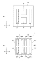
図1は、実施形態の発光ユニットの模式平面図である。
図2(a)は、実施形態の実装基板70の模式平面図である。
図2(b)は、実施形態の半導体発光装置1の模式平面図である。
図3は、実施形態の半導体発光装置1の模式断面図である。
FIG. 1 is a schematic plan view of the light emitting unit of the embodiment.
FIG. 2A is a schematic plan view of the
FIG. 2B is a schematic plan view of the semiconductor
FIG. 3 is a schematic cross-sectional view of the semiconductor
図2(b)は、半導体発光装置1の実装面を表し、図3に示す半導体発光装置1の下面図に対応する。
図1は、図2(b)に示す半導体発光装置1の実装面を、図2(a)に示す実装基板70のパッド81〜83に向けて、半導体発光装置1が実装基板70に実装された状態を表す。図1は、半導体発光装置1が実装基板70に実装された状態で半導体発光装置1の上面側(実装面の反対側)から見た模式平面図である。
FIG. 2B shows a mounting surface of the semiconductor
In FIG. 1, the semiconductor
半導体発光装置1は複数の発光素子10を有する。図1、図2(b)および図3に示す例では、半導体発光装置1は例えば2つの発光素子10を有する。複数の発光素子10はウェーハレベルで樹脂層25によってパッケージングされ、樹脂層25は複数の発光素子10を一体に支持している。
The semiconductor
半導体発光装置1を上面またはその反対側の実装面側から見た外形形状は、例えば矩形状である。その矩形の長手方向(第1方向X)に、例えば2つの発光素子10が並んでいる。それぞれの発光素子10は同じ構成をもつ。
The external shape of the semiconductor
図3に示すように、発光素子10は、発光層13を含む半導体層15を備えている。半導体層15は、厚み方向の一方の側(第1の側)15aと、その反対側の第2の側15b(図4)とを有する。
As shown in FIG. 3, the
図4は、1つの発光素子10における半導体層15の第2の側15bの模式平面図であり、p側電極16とn側電極17の平面レイアウトの一例を示す。
FIG. 4 is a schematic plan view of the
半導体層15の第2の側15bは、発光層13を含む部分(発光領域)15eと、発光層13を含まない部分15fとを有する。発光層13を含む部分15eは、半導体層15のうちで、発光層13が積層されている部分である。発光層13を含まない部分15fは、半導体層15のうちで、発光層13が積層されていない部分である。発光層13を含む部分15eは、発光層13が発光した光を外部に取り出し可能な積層構造となっている領域を示す。
The
第2の側15bにおいて、発光層13を含む部分15eの上に、第1電極としてp側電極16が設けられ、発光層を含まない部分15fの上に、第2電極としてn側電極17が設けられている。
On the
図4に示す例では、発光層13を含まない部分15fが発光層13を含む部分15eを囲んでおり、n側電極17がp側電極16を囲んでいる。
In the example shown in FIG. 4, the
p側電極16とn側電極17を通じて発光層13に電流が供給され、発光層13は発光する。そして、発光層13から放射される光は、第1の側15aから半導体発光装置1の外部に出射される。
A current is supplied to the
半導体層15の第2の側には、図3に示すように支持体100が設けられている。半導体層15、p側電極16およびn側電極17を含む発光素子10は、第2の側に設けられた支持体100によって支持されている。
A
半導体層15の第1の側15aには、半導体発光装置1の放出光に所望の光学特性を与える光学層として、蛍光体層30が設けられている。蛍光体層30は、複数の粒子状の蛍光体31を含む。蛍光体31は、発光層13の放射光により励起され、その放射光とは異なる波長の光を放射する。
On the
複数の蛍光体31は、結合材32により一体化されている。結合材32は、発光層13の放射光および蛍光体31の放射光を透過する。ここで「透過」とは、透過率が100%であることに限らず、光の一部を吸収する場合も含む。
The plurality of
半導体層15は、第1半導体層11と、第2半導体層12と、発光層13とを有する。発光層13は、第1半導体層11と、第2半導体層12との間に設けられている。第1半導体層11および第2半導体層12は、例えば、窒化ガリウムを含む。
The
第1半導体層11は、例えば、下地バッファ層、n型GaN層を含む。第2半導体層12は、例えば、p型GaN層を含む。発光層13は、青、紫、青紫、紫外光などを発光する材料を含む。発光層13の発光ピーク波長は、例えば、430〜470nmである。
The
半導体層15の第2の側は、凹凸形状に加工される。その凸部は、発光層13を含む部分15eであり、凹部は、発光層13を含まない部分15fである。発光層13を含む部分15eの表面は第2半導体層12の表面であり、第2半導体層12の表面にp側電極16が設けられている。発光層13を含まない部分15fの表面は第1半導体層11の表面であり、第1半導体層11の表面にn側電極17が設けられている。
The second side of the
半導体層15の第2の側において、発光層13を含む部分15eの面積は、発光層13を含まない部分15fの面積よりも広い。また、発光層13を含む部分15eの表面に設けられたp側電極16の面積は、発光層13を含まない部分15fの表面に設けられたn側電極17の面積よりも広い。これにより、広い発光面が得られ、光出力を高くできる。
On the second side of the
図4に示すように、n側電極17は例えば4本の直線部を有し、そのうちの1本の直線部には、その直線部の幅方向に突出したコンタクト部17cが設けられている。そのコンタクト部17cの表面には、図3に示すようにn側配線層22のビア22aが接続される。
As shown in FIG. 4, the n-
半導体層15の第2の側、p側電極16およびn側電極17は、図3に示すように、絶縁膜(第1絶縁膜)18で覆われている。絶縁膜18は、例えば、シリコン酸化膜などの無機絶縁膜である。絶縁膜18は、発光層13の側面及び第2の半導体層12の側面にも設けられ、それら側面を覆っている。
The second side of the
また、絶縁膜18は、半導体層15における第1の側15aから続く側面(第1半導体層11の側面)15cにも設けられ、その側面15cを覆っている。
The insulating
さらに、絶縁膜18は、半導体層15の側面15cの周囲のチップ外周部にも設けられている。チップ外周部に設けられた絶縁膜18は、第1の側15aで、側面15cから遠ざかる方向に延在している。
Furthermore, the insulating
第2の側の絶縁膜18上には、第1配線層としてのp側配線層21と、第2配線層としてのn側配線層22とが互いに分離して設けられている。絶縁膜18には、p側電極16に通じる複数の第1開口と、n側電極17のコンタクト部17cに通じる第2開口が形成される。
On the insulating
p側配線層21は、絶縁膜18上および第1開口の内部に設けられている。p側配線層21は、第1開口内に設けられたビア21aを介してp側電極16と電気的に接続されている。
The p-
n側配線層22は、絶縁膜18上および第2開口の内部に設けられている。n側配線層22は、第2開口内に設けられたビア22aを介してn側電極17のコンタクト部17cと電気的に接続されている。
The n-
p側配線層21及びn側配線層22が、第2の側の領域の大部分を占めて絶縁膜18上に広がっている。p側配線層21は、複数のビア21aを介してp側電極16と接続している。
The p-
また、半導体層15の側面15cを、絶縁膜18を介して反射膜51が覆っている。反射膜51は側面15cに接しておらず、半導体層15に対して電気的に接続されていない。反射膜51は、p側配線層21及びn側配線層22に対して分離している。反射膜51は、発光層13の放射光及び蛍光体31の放射光に対して反射性を有する。
Further, the
反射膜51、p側配線層21およびn側配線層22は、例えば銅膜を含む。反射膜51、p側配線層21およびn側配線層22は、図5に示す共通の金属膜60上に例えばめっき法により同時に形成される。反射膜51、p側配線層21およびn側配線層22のそれぞれの厚さは、金属膜60の厚さよりも厚い。
The
金属膜60は、絶縁膜18側から順に積層された、下地金属膜61と、密着層62と、シード層63とを有する。
The
下地金属膜61は、発光層13の放射光に対して高い反射性を有する例えばアルミニウム膜である。
The
シード層63は、めっきで銅を析出させるための銅膜である。密着層62は、アルミニウム及び銅の両方に対するぬれ性に優れた例えばチタン膜である。
The
なお、半導体層15の側面15cに隣接するチップ外周部においては、金属膜60上にめっき膜(銅膜)を形成せずに、金属膜60で反射膜51を形成してもよい。反射膜51は、少なくともアルミニウム膜61を含むことで、発光層13の放射光及び蛍光体31の放射光に対して高い反射率を有する。
Note that the
また、p側配線層21及びn側配線層22の下にも下地金属膜(アルミニウム膜)61が残されるので、第2の側の大部分の領域にアルミニウム膜61が広がって形成されている。これにより、蛍光体層30側に向かう光の量を増大できる。
Further, since the base metal film (aluminum film) 61 is also left under the p-
p側配線層21における半導体層15とは反対側の面には、第1金属ピラーとしてp側金属ピラー23が設けられている。p側配線層21及びp側金属ピラー23は、p側配線部(第1配線部)41を形成している。
A p-
n側配線層22における半導体層15とは反対側の面には、第2金属ピラーとしてn側金属ピラー24が設けられている。n側配線層22及びn側金属ピラー24は、n側配線部(第2配線部)43を形成している。
An n-
p側配線部41とn側配線部43との間には、第2絶縁膜として樹脂層25が設けられている。樹脂層25は、p側金属ピラー23の側面とn側金属ピラー24の側面に接するように、p側金属ピラー23とn側金属ピラー24との間に設けられている。すなわち、p側金属ピラー23とn側金属ピラー24との間に、樹脂層25が充填されている。
A
また、樹脂層25は、p側配線層21とn側配線層22との間、p側配線層21と反射膜51との間、およびn側配線層22と反射膜51との間に設けられている。
The
樹脂層25は、p側金属ピラー23の周囲およびn側金属ピラー24の周囲に設けられ、p側金属ピラー23の側面およびn側金属ピラー24の側面を覆っている。
The
また、樹脂層25は、半導体層15の側面15cに隣接するチップ外周部、および互いに分離された複数の半導体層15の間にも設けられ、反射膜51を覆っている。
The
p側金属ピラー23におけるp側配線層21とは反対側の端部(面)は、樹脂層25から露出し、外部回路と接続可能なp側外部端子23aとして機能する。n側金属ピラー24におけるn側配線層22とは反対側の端部(面)は、樹脂層25から露出し、外部回路と接続可能なn側外部端子24aとして機能する。後述するように、p側外部端子23a及びn側外部端子24aは、例えば、はんだ、または導電性の接合材を介して、図2(a)に示す実装基板70のパッド81〜83に接合される。
An end (surface) of the p-
図2(b)に示すように、p側外部端子23aは例えば矩形状に形成され、n側外部端子24aは、p側外部端子23aの矩形と同じサイズの矩形における2つの角を切り欠いた形状に形成されている。これにより、外部端子の極性を判別できる。なお、n側外部端子24aを矩形状にし、p側外部端子23aを矩形の角を切り欠いた形状にしてもよい。
As shown in FIG. 2B, the p-side
p側外部端子23aとn側外部端子24aとの間隔は、絶縁膜18上におけるp側配線層21とn側配線層22との間隔よりも広い。p側外部端子23aとn側外部端子24aとの間隔は、実装時のはんだの広がりよりも大きくする。これにより、はんだを通じた、p側外部端子23aとn側外部端子24aとの間の短絡を防ぐことができる。
The distance between the p-side external terminal 23 a and the n-side external terminal 24 a is wider than the distance between the p-
これに対し、p側配線層21とn側配線層22との間隔は、プロセス上の限界まで狭くすることができる。このため、p側配線層21の面積、およびp側配線層21とp側金属ピラー23との接触面積の拡大を図れる。これにより、発光層13の熱の放散を促進できる。
On the other hand, the distance between the p-
また、複数のビア21aを通じてp側配線層21がp側電極16と接する面積は、ビア22aを通じてn側配線層22がn側電極17と接する面積よりも広い。これにより、発光層13に流れる電流の分布を均一化できる。
Further, the area where the p-
絶縁膜18上で広がるn側配線層22の面積は、n側電極17の面積よりも広くできる。そして、n側配線層22の上に設けられるn側金属ピラー24の面積(n側外部端子24aの面積)をn側電極17よりも広くできる。これにより、実装に十分なn側外部端子24aの面積を確保しつつ、n側電極17の面積を小さくすることが可能となる。すなわち、半導体層15における発光層13を含まない部分15fの面積を縮小し、発光層13を含む部分(発光領域)15eの面積を広げて光出力を向上させることが可能となる。
The area of the n-
第1の半導体層11は、n側電極17及びn側配線層22を介してn側金属ピラー24と電気的に接続されている。第2の半導体層12は、p側電極16及びp側配線層21を介してp側金属ピラー23と電気的に接続されている。
The
p側金属ピラー23の厚さ(p側配線層21とp側外部端子23aとを結ぶ方向の厚さ)は、p側配線層21の厚さよりも厚い。n側金属ピラー24の厚さ(n側配線層22とn側外部端子24aとを結ぶ方向の厚さ)は、n側配線層22の厚さよりも厚い。p側金属ピラー23、n側金属ピラー24および樹脂層25のそれぞれの厚さは、半導体層15よりも厚い。
The thickness of the p-side metal pillar 23 (thickness in the direction connecting the p-
金属ピラー23、24のアスペクト比(平面サイズに対する厚みの比)は、1以上であっても良いし、1より小さくても良い。すなわち、金属ピラー23、24は、その平面サイズより厚くても良いし、薄くても良い。
The
p側配線層21、n側配線層22、p側金属ピラー23、n側金属ピラー24および樹脂層25を含む支持体100の厚さは、半導体層15、p側電極16およびn側電極17を含む発光素子(LEDチップ)10の厚さよりも厚い。
The thickness of the
半導体層15は、図示しない基板上にエピタキシャル成長法により形成される。その基板は、支持体100を形成した後に除去され、半導体層15は第1の側15aに基板を含まない。半導体層15は、剛直な板状の基板にではなく、金属ピラー23、24と樹脂層25との複合体からなる支持体100によって支持されている。
The
p側配線部41及びn側配線部43の材料として、例えば、銅、金、ニッケル、銀などを用いることができる。これらのうち、銅を用いると、良好な熱伝導性、高いマイグレーション耐性および絶縁材料に対する密着性を向上させることができる。
As a material of the p-
樹脂層25は、p側金属ピラー23およびn側金属ピラー24を補強する。樹脂層25は、実装基板70と熱膨張率が同じもしくは近いものを用いるのが望ましい。そのような樹脂層25として、例えば、エポキシ樹脂を主に含む樹脂、シリコーン樹脂を主に含む樹脂、フッ素樹脂を主に含む樹脂を挙げることができる。
The
また、樹脂層25におけるベースとなる樹脂に遮光材(光吸収剤、光反射剤、光散乱剤など)が含まれ、樹脂層25は発光層13が発光する光に対して遮光性を有する。これにより、支持体100の側面及び実装面側からの光漏れを抑制することができる。
Further, the resin serving as a base in the
半導体発光装置1を実装基板70に実装するときの熱サイクルにより、p側外部端子23aおよびn側外部端子24aを実装基板70のパッド81〜83に接合させるはんだに起因する応力が半導体層15に加わる。p側金属ピラー23、n側金属ピラー24および樹脂層25は、その応力を吸収し緩和する。特に、半導体層15よりも柔軟な樹脂層25を支持体100の一部として用いることで、応力緩和効果を高めることができる。
Due to the thermal cycle when the semiconductor
反射膜51は、p側配線部41及びn側配線部43に対して分離している。このため、実装時にp側金属ピラー23及びn側金属ピラー24に加わる応力は、反射膜51には伝達されない。したがって、反射膜51の剥離を抑制することができる。また、半導体層15の側面15c側に加わる応力を抑制することができる。
The
半導体層15の形成に用いた基板は、半導体層15から除去される。これにより、半導体発光装置1は低背化される。また、基板の除去により、半導体層15の第1の側15aに微小凹凸を形成することができ、光取り出し効率の向上を図れる。
The substrate used for forming the
例えば、第1の側15aに対して、アルカリ系溶液を使ったウェットエッチングを行い微小凹凸を形成する。これにより、第1の側15aでの全反射成分を減らして、光取り出し効率を向上できる。
For example, fine unevenness is formed on the
基板が除去された後、第1の側15a上に絶縁膜19を介して蛍光体層30が形成される。絶縁膜19は、半導体層15と蛍光体層30との密着性を高め、例えば、シリコン酸化膜、シリコン窒化膜である。
After the substrate is removed, the
蛍光体層30は、結合材32中に複数の粒子状の蛍光体31が分散された構造を有する。結合材32には、例えば、シリコーン樹脂を用いることができる。
The
蛍光体層30は、半導体層15の側面15cの周囲のチップ外周部上、および発光素子10と発光素子10との間の領域上にも形成される。チップ外周部および発光素子10間領域においては、絶縁膜(例えばシリコン酸化膜)18上に蛍光体層30が設けられている。
The
半導体層15と半導体層15との間の領域(チップ間領域)において、絶縁膜18は、連続していることに限らず、図13に示すように分断してもよい。樹脂層25の熱膨張係数によっては絶縁膜18にクラックが生じる場合があり得るが、図13に示すように、チップ間領域の絶縁膜18をパターニングにより分断することで、クラックを抑制できる。
In the region between the
蛍光体層30は、発光素子10よりも上の領域側に限定され、半導体層15の第2の側、金属ピラー23、24の周囲、および支持体100の側面にまわりこんで形成されない。蛍光体層30の側面と、支持体100の側面(樹脂層25の側面)とが揃っている。
The
光を外部に取り出さない実装面側には蛍光体層30が無駄に形成されず、コスト低減が図れる。また、第1の側15aに基板がなくても、第2の側に広がるp側配線層21及びn側配線層22を介して発光層13の熱を実装基板70側に放散させることができ、小型でありながらも放熱性に優れている。
The
一般的なフリップチップ実装では、LEDチップを実装基板にバンプなどを介して実装した後に、チップ全体を覆うように蛍光体層が形成される。あるいは、バンプ間に樹脂がアンダーフィルされる。 In general flip chip mounting, a phosphor layer is formed so as to cover the entire chip after the LED chip is mounted on a mounting substrate via bumps or the like. Alternatively, the resin is underfilled between the bumps.
これに対して実施形態によれば、実装前の状態で、p側金属ピラー23の周囲及びn側金属ピラー24の周囲には、蛍光体層30と異なる樹脂層25が設けられ、実装面側に応力緩和に適した特性を与えることができる。また、実装面側にすでに樹脂層25が設けられているため、実装後のアンダーフィルが不要となる。
On the other hand, according to the embodiment, the
第1の側15aには、光取り出し効率、色変換効率、配光特性などを優先した設計の層が設けられ、実装面側には、実装時の応力緩和や、基板に代わる支持体としての特性を優先した層が設けられる。例えば、樹脂層25は、ベースとなる樹脂にシリカ粒子などのフィラーが高密度充填された構造を有し、支持体として適切な硬さに調整されている。
The
発光層13から第1の側15aに放射された光は蛍光体層30に入射し、一部の光は蛍光体31を励起し、発光層13の光と、蛍光体31の光との混合光として例えば白色光が得られる。
The light emitted from the
ここで、第1の側15a上に基板があると、蛍光体層30に入射せずに、基板の側面から外部に漏れる光が生じる。すなわち、基板の側面から発光層13の光の色みの強い光が漏れ、蛍光体層30を上面から見た場合に、外縁側に青色光のリングが見える現象など、色割れや色ムラの原因になり得る。
Here, if there is a substrate on the
これに対して、実施形態によれば、第1の側15aと蛍光体層30との間には、半導体層15の成長に用いた基板がないため、基板側面から発光層13の光の色みが強い光が漏れることによる色割れや色ムラを防ぐことができる。
On the other hand, according to the embodiment, since there is no substrate used for the growth of the
さらに、実施形態によれば、半導体層15の側面15cに、絶縁膜18を介して反射膜51が設けられている。発光層13から半導体層15の側面15cに向かった光は、反射膜51で反射し、外部に漏れない。このため、基板が第1の側15aにない特徴とあいまって、半導体発光装置の側面側からの光漏れによる色割れや色ムラを防ぐことができる。
Furthermore, according to the embodiment, the
反射膜51と、半導体層15の側面15cとの間に設けられた絶縁膜18は、反射膜51に含まれる金属の半導体層15への拡散を防止する。これにより、半導体層15の例えばGaNの金属汚染を防ぐことができ、半導体層15の劣化を防ぐことができる。
The insulating
また、反射膜51と蛍光体層30との間、および樹脂層25と蛍光体層30との間に設けられた絶縁膜18は、反射膜51と蛍光体層30との密着性、および樹脂層25と蛍光体層30との密着性を高める。
In addition, the insulating
絶縁膜18は、例えばシリコン酸化膜、シリコン窒化膜などの無機絶縁膜である。すなわち、半導体層15の第1の側15a、第2の側、第1の半導体層11の側面15c、第2の半導体層12の側面、発光層13の側面は、無機絶縁膜で覆われている。無機絶縁膜は半導体層15を囲み、金属や水分などから半導体層15をブロックする。
The insulating
複数の発光素子10間にまたがって蛍光体層30が広がっている。蛍光体層30上には、必要に応じてレンズ50が設けられる。レンズ50は、例えば透明樹脂で形成される。図3には、凸レンズを例示するが、凹レンズであってもよい。
The
複数の発光素子10は共通の樹脂層25でパッケージングされている。そのため、複数の発光素子10をカバーするように一体型のレンズ形成が可能となる。実施形態のマルチチップパッケージによれば、1つの発光素子ごとに分離された個別パッケージ上へのレンズ形成ではできないレンズ形状による配光特性制御が可能となる。
The plurality of
発光素子10、支持体100、蛍光体層30およびレンズ50を形成する工程は、多数の半導体層15を含むウェーハ状態で行われる。その後、ウェーハは、少なくとも2つの発光素子10(半導体層15)を含む複数の半導体発光装置1に分離される。半導体層15と半導体層15との間の領域(ダイシング領域)で切断される。ダイシング領域を任意に選択することで、1つの半導体発光装置に含まれる発光素子10(半導体層10)の数を選択できる。
The process of forming the
ダイシングされるまでの各工程は、ウェーハ状態で一括して行われるため、分離された個々の半導体発光装置ごとに、配線層の形成、ピラーの形成、樹脂層によるパッケージング、および蛍光体層の形成を行う必要がなく、大幅なコストの低減が可能になる。 Each process until dicing is performed collectively in a wafer state, and therefore, for each separated semiconductor light emitting device, formation of a wiring layer, formation of pillars, packaging with a resin layer, and phosphor layer There is no need to form, and a significant cost reduction is possible.
ウェーハ状態で、支持体100および蛍光体層30を形成した後に、それらが切断されるため、蛍光体層30の側面と、支持体100の側面(樹脂層25の側面)とは揃い、それら側面が分離された半導体発光装置1の側面を形成する。したがって、基板がないこともあいまって、小型の半導体発光装置を提供することができる。
After the
実施形態によれば、半導体層15の第1の側15aに光学層が設けられている。光学層と、実装面(外部端子23a、24aが設けられた面)との間に、半導体層15及び電極16、17を含む発光素子10が設けられている。
According to the embodiment, an optical layer is provided on the
光学層としては、蛍光体層に限らず、散乱層であってもよい。散乱層は、発光層13の放射光を散乱させる複数の粒子状の散乱材(例えばチタン化合物)と、複数の散乱材を一体化し発光層13の放射光を透過させる結合材(例えば樹脂層)とを含む。
The optical layer is not limited to the phosphor layer, and may be a scattering layer. The scattering layer includes a plurality of particulate scattering materials (for example, titanium compounds) that scatter the emitted light of the
前述した半導体発光装置1は、図2(a)に示す実装基板70に実装される。実装基板70は、第1パッド81と、第2パッド82と、第3パッド83とを有する。第1パッド81、第2パッド82および第3パッド83は、金属(例えば銅)で形成されている。第1パッド81、第2パッド82および第3パッド83は、絶縁体上に形成されている。第1パッド81、第2パッド82および第3パッド83のそれぞれは、周囲を絶縁体で囲まれている。
The semiconductor
第1パッド81、第2パッド82および第3パッド83は、第1方向Xに互いに離間して並んでいる。第1パッド81と第2パッド82との間に、第3パッド83が設けられている。
The
第1パッド81と半導体発光装置1のp側外部端子23aとは合同図形の関係にあり、第2パッド82と半導体発光装置1のn側外部端子24aとは合同図形の関係にある。
The
第1パッド81は第1方向Xに対して直交する第2方向Yに延びる長辺を有する矩形状に形成されている。第2パッド82は、第1パッド81の矩形と同じサイズの矩形における2つの角を切り欠いた形状に形成されている。これにより、パッドの極性を判別できる。
The
なお、半導体発光装置1のn側外部端子24aを矩形状にし、p側外部端子23aを矩形の角を切り欠いた形状にした場合、第2パッド82を矩形状にし、第1パッド81を矩形の角を切り欠いた形状にすることができる。
When the n-side
第3パッド83は例えば四角形状に形成されている。第3パッド83の面積は、第1パッド81の面積および第2パッド82の面積よりも広い。第3パッド83を第1方向Xに2等分する中心線Cに対して、第1パッド81と第2パッド82は対称配置されている。
The
図2(b)に示すように、半導体発光装置1において、2つの発光素子10は第1方向Xに並んでいる。それぞれの発光素子10は、1つのp側外部端子23aと1つのn側外部端子24aを有する。1つの発光素子10においてp側外部端子23aとn側外部端子24aは第1方向Xに並んでいる。
As shown in FIG. 2B, in the semiconductor
したがって、2つの発光素子10の4つの外部端子23a、24aが第1方向Xに並んでいる。p側外部端子23aとn側外部端子24aは交互に第1方向Xに並んでいる。
Accordingly, the four
図2(b)において左側の発光素子10のp側外部端子23aは、左側の発光素子10のp側電極16に接続され、左側の発光素子10のn側外部端子24aは、左側の発光素子10のn側電極17に接続されている。
In FIG. 2B, the p-side
図2(b)において右側の発光素子10のp側外部端子23aは、右側の発光素子10のp側電極16に接続され、右側の発光素子10のn側外部端子24aは、右側の発光素子10のn側電極17に接続されている。
In FIG. 2B, the p-side
第1方向Xに並んだ4つの外部端子23a、24aのうち、第1方向Xの一方の端のp側外部端子23aは、実装基板70の第1パッド81に例えばはんだを介して接合される。すなわち、図2(b)において左側の発光素子10のp側外部端子23aは第1パッド81に接合される。
Of the four
4つの外部端子23a、24aのうち、第1方向Xの他方の端のn側外部端子24aは、実装基板70の第2パッド82に例えばはんだを介して接合される。すなわち、図2(b)において右側の発光素子10のn側外部端子24aは第2パッド82に接合される。
Of the four
第1パッド81に接合される左端のp側外部端子23aと、第2パッド82に接合される右端のn側外部端子24aとの間の、2つの外部端子23a、24aは、実装基板70の第3パッド83にはんだを介して接合される。それら2つの外部端子23a、24aが共通の第3パッド83に接合される。
Two
したがって、第1方向Xで隣り合う2つの発光素子10のうち一方の(図2(b)において左側の)発光素子10のn側外部端子24aと、他方の(図2(b)において右側の)発光素子10のp側外部端子23aとが、共通の第3パッド83に接合される。
Therefore, of the two
第1パッド81には、実装基板70に形成された図示しない配線を通じてアノード電位が与えられる。第2パッド82には、実装基板70に形成された図示しない配線を通じて、アノード電位より低いカソード電位が与えられる。
An anode potential is applied to the
第3パッド83は電気的にどこにも接続されず、その電位はフローティングである。一方(左側)の発光素子10のn側外部端子24aと、他方(右側)の発光素子10のp側外部端子23aは、第3パッド83を介して電気的に接続されている。
The
電流は、第1パッド81、それに接合された左端のp側外部端子23a、左側の発光素子10のp側金属ピラー23、p側配線層21、p側電極16、および第2半導体層12を経由して発光層13に供給され、さらに、左側の発光素子10の第1半導体層11、n側電極17、n側配線層22、n側金属ピラー24、およびn側外部端子24aを流れる。
The current flows through the
さらに、電流は、第3パッド83、右側の発光素子10のp側外部端子23a、p側金属ピラー23、p側配線層21、p側電極16、および第2半導体層12を経由して右側の発光素子10の発光層13に供給され、さらに、右側の発光素子10の第1半導体層11、n側電極17、n側配線層22、n側金属ピラー24、n側外部端子24a、およびこのn側外部端子24aが接合された第2パッド82を流れる。
Furthermore, the current passes through the
すなわち、図1に模式的にダイオードの回路記号で表すように、2つの発光素子10は第1パッド81と第2パッド82との間で直列接続されている。
That is, as schematically represented by a circuit symbol of a diode in FIG. 1, the two
2つの発光素子10は実装基板70に形成された第3パッド83を通じて電気的に接続されている。パッケージ内の配線層で2つの発光素子10を接続する必要がなく、マルチチップパッケージの半導体発光装置1の構造を簡単にできる。
The two
第3パッド83の面積は、第1パッド81の面積および第2パッド82の面積よりも広い。また、第3パッド83の面積は、第1パッド81の面積と第2パッド82の面積とを合わせた面積よりも広い。さらに、第3パッド83の面積は、1つのp側外部端子23aの面積と1つのn側外部端子24aの面積とを合わせた面積よりも広い。そのような広い第3パッド83を通じて、半導体発光装置1の熱を実装基板70側に効率よく逃がすことができる。
The area of the
第1パッド81と第3パッド83との間の距離、すなわち、図2(b)において左側の発光素子10のp側外部端子23aとn側外部端子24aとの間の距離は、はんだを介したショートを起こしにくくするために200μm以上が望ましい。同様に、第2パッド82と第3パッド83との間の距離、すなわち、図2(b)において右側の発光素子10のp側外部端子23aとn側外部端子24aとの間の距離も、はんだを介したショートを起こしにくくするために200μm以上が望ましい。
The distance between the
これに対して一方(左側)の発光素子10のn側外部端子24aと、他方(右側)の発光素子10のp側外部端子23aは共通の第3パッド83に接合されるため、それら隣り合う発光素子10の隣り合う外部端子23a、24a間の距離には制約がなく、設計自由度が高い。
On the other hand, the n-side
1つのパッケージに1つの発光素子を含むシングルチップ構造の2つの半導体発光装置を隣接させて実装基板に実装する場合には、半導体発光装置を保持するコレットが隣の半導体発光装置にぶつからないように、実装された半導体発光装置間にはクリアランスが必要となる。したがって、個々の半導体発光装置のパッケージサイズを小型化しても、実装スペースはコレットサイズの制約を受ける。 When two semiconductor light emitting devices having a single chip structure including one light emitting element are mounted adjacent to each other on a mounting substrate, a collet holding the semiconductor light emitting device does not collide with an adjacent semiconductor light emitting device. A clearance is required between the mounted semiconductor light emitting devices. Therefore, even if the package size of each semiconductor light emitting device is reduced, the mounting space is limited by the collet size.
これに対し、実施形態によれば、1つのパッケージ内で複数の発光素子10を近接させることができるため、1つずつ個片化された複数の発光素子を実装するよりも、実装基板上での実装スペースを小さくできる。
On the other hand, according to the embodiment, since a plurality of
図6は、実装基板のパッドの他の例を示す模式平面図である。 FIG. 6 is a schematic plan view showing another example of pads on the mounting board.
図6によれば、第3パッド83に一体に第4パッド84が設けられ、放熱面積が図2(a)に示す例よりも広くなっている。第4パッド84は、第1パッド81および第2パッド82を避けるように、第3パッド83から第2方向Yに広がっている。
According to FIG. 6, the
図7は、他の実施形態の発光ユニットの模式平面図である。
図8(a)は、他の実施形態の実装基板70の模式平面図である。
図8(b)は、他の実施形態の半導体発光装置1の模式平面図である。
FIG. 7 is a schematic plan view of a light emitting unit according to another embodiment.
FIG. 8A is a schematic plan view of a mounting
FIG. 8B is a schematic plan view of the semiconductor
図7、図8(a)および図8(b)は、それぞれ、図1、図2(a)および図2(b)に対応する図であり、同じ要素には同じ符号を付している。 7, FIG. 8 (a) and FIG. 8 (b) are diagrams corresponding to FIG. 1, FIG. 2 (a) and FIG. 2 (b), respectively, and the same elements are denoted by the same reference numerals. .
図8(b)に示す半導体発光装置1は例えば4つの発光素子10を有する。4つの発光素子10はウェーハレベルで樹脂層25によってパッケージングされ、樹脂層25は4つの発光素子10を一体に支持している。
The semiconductor
第1方向Xに並んだ2つの発光素子10のグループ(列)が、第1方向Xに対して直交する第2方向Yに2列並んでいる。
Two groups (rows) of the
第1方向Xに並んだ2つの発光素子10のグループ(列)において、p側外部端子23aとn側外部端子24aが交互に第1方向Xに並んでいる。
In a group (column) of two light emitting
実装基板70には、1つの第1パッド81と、1つの第2パッド82と、2つの第3パッド83とが形成されている。
On the mounting
2つの第3パッド83は、第1パッド81と第2パッド82との間で、第2方向Yに互いに離間して並んでいる。
The two
第1方向Xに一列に並んだ4つの外部端子23a、24aのうち、第1方向Xの一方の端のp側外部端子23aは、実装基板70の第1パッド81に例えばはんだを介して接合される。すなわち、図8(b)において左側の2つの発光素子10の2つのp側外部端子23aは第1パッド81に接合される。
Of the four
第1方向Xに一列に並んだ4つの外部端子23a、24aのうち、第1方向Xの他方の端のn側外部端子24aは、実装基板70の第2パッド82に例えばはんだを介して接合される。すなわち、図8(b)において右側の2つの発光素子10の2つのn側外部端子24aは第2パッド82に接合される。
Of the four
第1パッド81に接合される左端のp側外部端子23aと、第2パッド82に接合される右端のn側外部端子24aとの間の、外部端子23a、24aは、実装基板70の第3パッド83にはんだを介して接合される。
The
図8(b)において上側の列で第1方向Xで隣り合う2つの発光素子10のうち一方(左側)の発光素子10のn側外部端子24aと、他方(右側)の発光素子10のp側外部端子23aとが、2つの第3パッド83のうちの一方に接合される。
In FIG. 8B, of the two
図8(b)において下側の列で第1方向Xで隣り合う2つの発光素子10のうち一方(左側)の発光素子10のn側外部端子24aと、他方(右側)の発光素子10のp側外部端子23aとが、2つの第3パッド83のうちの他方に接合される。
8B, the n-side
第1パッド81には、実装基板70に形成された図示しない配線を通じてアノード電位が与えられる。第2パッド82には、実装基板70に形成された図示しない配線を通じて、アノード電位より低いカソード電位が与えられる。
An anode potential is applied to the
第3パッド83は電気的にどこにも接続されず、その電位はフローティングである。第1方向Xで隣り合う一方(左側)の発光素子10のn側外部端子24aと、他方(右側)の発光素子10のp側外部端子23aは、第3パッド83を介して電気的に接続されている。
The
したがって、図7に模式的にダイオードの回路記号で表すように、第1方向Xに並んだ2つの発光素子10は第1パッド81と第2パッド82との間で直列接続されている。また、上の列と下の列は、第1パッド81と第2パッド82との間に並列接続されている。
Therefore, as schematically represented by a circuit symbol of a diode in FIG. 7, the two
第1方向Xで隣り合う一方(左側)の発光素子10のn側外部端子24aと、他方(右側)の発光素子10のp側外部端子23aは共通の第3パッド83に接合されるため、それら隣り合う発光素子10の隣り合う外部端子23a、24a間の距離には制約がなく、設計自由度が高い。
Since the n-side
また、1つのパッケージ内で複数の発光素子10を近接させることができるため、1つずつ個片化された複数の発光素子を実装するよりも、実装基板上での実装スペースを小さくできる。
In addition, since the plurality of
図9は、さらに他の実施形態の発光ユニットの模式平面図である。
図10(a)は、さらに他の実施形態の実装基板70の模式平面図である。
図10(b)は、さらに他の実施形態の半導体発光装置1の模式平面図である。
FIG. 9 is a schematic plan view of a light emitting unit according to still another embodiment.
FIG. 10A is a schematic plan view of a mounting
FIG. 10B is a schematic plan view of the semiconductor
図9、図10(a)および図10(b)は、それぞれ、図7、図8(a)および図8(b)に対応する図であり、同じ要素には同じ符号を付している。 9, FIG. 10 (a) and FIG. 10 (b) are diagrams corresponding to FIG. 7, FIG. 8 (a) and FIG. 8 (b), respectively, and the same elements are denoted by the same reference numerals. .
図10(b)に示す半導体発光装置1は例えば6つの発光素子10を有する。6つの発光素子10はウェーハレベルで樹脂層25によってパッケージングされ、樹脂層25は6つの発光素子10を一体に支持している。
The semiconductor
第1方向Xには3つの発光素子10が並んでいる。第1方向Xに並んだ3つの発光素子10のグループ(列)が、第1方向Xに対して直交する第2方向Yに2列並んでいる。
Three
第1方向Xに並んだ3つの発光素子10のグループ(列)において、p側外部端子23aとn側外部端子24aが交互に第1方向Xに並んでいる。
In a group (column) of three light emitting
実装基板70には、2つの第1パッド81と、2つの第2パッド82と、4つの第3パッド83とが形成されている。
On the mounting
2つの第1パッド81は第2方向Yに互いに離間して並んでいる。2つの第2パッド82は第2方向Yに互いに離間して並んでいる。あるいは、図8(a)に示す例のように、第2方向Yにつながった1つの第1パッド81と、第2方向Yにつながった1つの第2パッド82であってもよい。この場合、パッド面積が増え、放熱性が向上する。
The two
第1パッド81と第2パッド82との間には、第1方向Xに並んだ2つの第3パッド83および第2方向Yに並んだ2つの第3パッド83の合わせて4つの第3パッド83が設けられている。
Between the
第1方向Xに一列に並んだ3つの発光素子10の6つの外部端子23a、24aのうち、第1方向Xの一方の端のp側外部端子23aは、実装基板70の第1パッド81に例えばはんだを介して接合される。すなわち、図10(b)において第2方向Yに並んだ左端の2つの発光素子10の2つのp側外部端子23aは第1パッド81に接合される。
Of the six
第1方向Xに一列に並んだ6つの外部端子23a、24aのうち、第1方向Xの他方の端のn側外部端子24aは、実装基板70の第2パッド82に例えばはんだを介して接合される。すなわち、図10(b)において第2方向Yに並んだ右端の2つの発光素子10の2つのn側外部端子24aは第2パッド82に接合される。
Of the six
第1パッド81に接合される左端のp側外部端子23aと、第2パッド82に接合される右端のn側外部端子24aとの間の、外部端子23a、24aは、実装基板70の第3パッド83にはんだを介して接合される。
The
図10(b)において上側の列の左端およびその右隣の2つの発光素子10のうち一方(左側)の発光素子10のn側外部端子24aと、他方(右側)の発光素子10のp側外部端子23aとが、図10(a)に示す第1パッド81の横の2つの第3パッド83のうちの一方に接合される。
In FIG. 10B, the n-side external terminal 24 a of one (left side) light-emitting
図10(b)において下側の列の左端およびその右隣の2つの発光素子10のうち一方(左側)の発光素子10のn側外部端子24aと、他方(右側)の発光素子10のp側外部端子23aとが、図10(a)に示す第1パッド81の横の2つの第3パッド83のうちの他方に接合される。
In FIG. 10B, among the two
図10(b)において上側の列の右端およびその左隣の2つの発光素子10のうち一方(左側)の発光素子10のn側外部端子24aと、他方(右側)の発光素子10のp側外部端子23aとが、図10(a)に示す第2パッド82の横の2つの第3パッド83のうちの一方に接合される。
10B, the n-side
図10(b)において下側の列の右端およびその左隣の2つの発光素子10のうち一方(左側)の発光素子10のn側外部端子24aと、他方(右側)の発光素子10のp側外部端子23aとが、図10(a)に示す第2パッド82の横の2つの第3パッド83のうちの他方に接合される。
In FIG. 10B, the n-side external terminal 24 a of one (left side)
第1パッド81には、実装基板70に形成された図示しない配線を通じてアノード電位が与えられる。第2パッド82には、実装基板70に形成された図示しない配線を通じて、アノード電位より低いカソード電位が与えられる。
An anode potential is applied to the
第3パッド83は電気的にどこにも接続されず、その電位はフローティングである。第1方向Xで隣り合う2つの発光素子10の一方の発光素子10のn側外部端子24a(p側外部端子23a)と、他方の発光素子10のp側外部端子23a(n側外部端子24a)は、第3パッド83を介して電気的に接続されている。
The
したがって、図9に模式的にダイオードの回路記号で表すように、第1方向Xに並んだ3つの発光素子10は第1パッド81と第2パッド82との間で直列接続されている。
Therefore, as schematically represented by a circuit symbol of a diode in FIG. 9, the three
第1方向Xで隣り合う一方の発光素子10のn側外部端子24a(p側外部端子23a)と、他方の発光素子10のp側外部端子23a(n側外部端子24a)は共通の第3パッド83に接合されるため、それら隣り合う発光素子10の隣り合う外部端子23a、24a間の距離には制約がなく、設計自由度が高い。
The n-side
また、1つのパッケージ内で複数の発光素子10を近接させることができるため、1つずつ個片化された複数の発光素子を実装するよりも、実装基板上での実装スペースを小さくできる。
In addition, since the plurality of
図11は、他の実施形態の半導体発光装置2の模式断面図である。
図12は、半導体発光装置2の模式平面図である。図12は、半導体発光装置2の実装面を表し、図11に示す半導体発光装置2の下面図に対応する。
FIG. 11 is a schematic cross-sectional view of a semiconductor
FIG. 12 is a schematic plan view of the semiconductor
半導体発光装置2は、第3金属ピラー26および第3外部端子26aを有する点で、上記実施形態の半導体発光装置1と異なる。半導体発光装置2において、半導体発光装置1と同じ要素には同じ符号を付し、その詳細な説明は省略する。
The semiconductor
半導体発光装置2は複数の発光素子10を有する。図11、図12に示す例では、半導体発光装置2は例えば2つの発光素子10を有する。複数の発光素子10はウェーハレベルで樹脂層25によってパッケージングされ、樹脂層25は複数の発光素子10を一体に支持している。
The semiconductor
半導体発光装置2を上面またはその反対側の実装面側から見た外形形状は、例えば矩形状である。その矩形の長手方向(第1方向X)に、例えば2つの発光素子10が並んでいる。
The external shape of the semiconductor
第1方向Xで隣り合う2つの発光素子10の一方の発光素子10は、p側金属ピラー23およびp側外部端子23aを有し、n側金属ピラー24およびn側外部端子24aを持たない。他方の発光素子10は、逆に、p側金属ピラー23およびp側外部端子23aを持たず、n側金属ピラー24およびn側外部端子24aを有する。
One of the two
第1方向Xで隣り合う2つの発光素子10に共通に第3金属ピラー26が設けられている。第3金属ピラー26は、p側金属ピラー23およびn側金属ピラー24と同じ材料で形成され、同じ方法(例えばめっき法)で同時に形成される。
A
第3金属ピラー26は、第1方向Xで隣り合う2つの発光素子10の一方の発光素子10のn側配線層22と、他方の発光素子10のp側配線層21とを接続している。
The
第3金属ピラー26の端部(図11における下面)は、樹脂層25から露出し、第3外部端子26aとして機能する。
The end (the lower surface in FIG. 11) of the
図12に示すように、2つの発光素子10が第1方向Xに並んでいる。一方の発光素子10のp側外部端子23aは第1方向Xの一方の端に設けられ、他方の発光素子10のn側外部端子24aは第1方向Xの他方の端に設けられている。それら第1方向Xの両端のp側外部端子23aとn側外部端子24aとの間に、第3外部端子26aが設けられている。
As shown in FIG. 12, the two
第3外部端子26aは例えば四角形状に形成されている。第3外部端子26aの面積は、p側外部端子23aの面積およびn側外部端子24aの面積よりも広い。第3外部端子26aを第1方向Xに2等分する中心線Cに対して、p側外部端子23aとn側外部端子24aは対称配置されている。
The third
図11、12において左側の発光素子10のp側外部端子23aは、左側の発光素子10のp側電極16に接続され、左側の発光素子10のn側電極17は、第3外部端子26aに接続されている。
11 and 12, the p-side
図11、12において右側の発光素子10のn側外部端子24aは、右側の発光素子10のn側電極17に接続され、右側の発光素子10のp側電極16は、第3外部端子26aに接続されている。
11 and 12, the n-side
図11、12に示す半導体発光装置2は、例えば図2(a)に示す実装基板に実装することができる。
The semiconductor
p側外部端子23aは、実装基板70の第1パッド81に例えばはんだを介して接合される。n側外部端子24aは、実装基板70の第2パッド82に例えばはんだを介して接合される。p側外部端子23aとn側外部端子24aとの間の第3外部端子26aは、実装基板70の第3パッド83にはんだを介して接合される。
The p-side
第1パッド81には、実装基板70に形成された図示しない配線を通じてアノード電位が与えられる。第2パッド82には、実装基板70に形成された図示しない配線を通じて、アノード電位より低いカソード電位が与えられる。
An anode potential is applied to the
第3パッド83は電気的にどこにも接続されず、その電位はフローティングである。一方(左側)の発光素子10のn側電極17と、他方(右側)の発光素子10のp側電極16とは、第3金属ピラー26、第3外部端子26a、および第3パッド83を介して電気的に接続されている。
The
電流は、第1パッド81、それに接合された一方の発光素子10のp側外部端子23a、p側金属ピラー23、p側配線層21、p側電極16、および第2半導体層12を経由して発光層13に供給され、さらに、その一方の発光素子10の第1半導体層11、n側電極17、n側配線層22、第3金属ピラー26、および第3外部端子26aを流れる。
The current passes through the
さらに、電流は、第3パッド83、他方の発光素子10のp側配線層21、p側電極16、および第2半導体層12を経由して他方の発光素子10の発光層13に供給され、さらに、他方の発光素子10の第1半導体層11、n側電極17、n側配線層22、n側金属ピラー24、n側外部端子24a、および第2パッド82を流れる。
Further, the current is supplied to the
すなわち、図12に模式的にダイオードの回路記号で表すように、半導体発光装置2の2つの発光素子10は第1パッド81と第2パッド82との間で直列接続されている。
That is, as schematically represented by a circuit symbol of a diode in FIG. 12, the two
2つの発光素子10は、第3外部端子26aを含む第3金属ピラー26を通じて電気的に接続されている。2つの発光素子10は実装基板70に実装されていない状態で、はんだを介さずに、はんだよりも熱伝導率が高い例えば銅で形成された第3金属ピラー26を通じて電気的に接続されている。さらに、パッケージ内の配線層21、22よりも厚い第3金属ピラー26を通じて2つの発光素子10は接続されている。
The two
すなわち、はんだや薄い配線層よりも放熱性に優れた厚い金属ピラー26を通じて複数チップが接続されている。このため、複数のチップ(半導体層15)間の温度特性差(発光特性差)を小さくできる。
That is, a plurality of chips are connected through a
また、発光素子10の熱を、p側外部端子23aおよびn側外部端子24aよりも広い第3外部端子26aおよび第3パッド83を通じて、実装基板70側へ効率よく放熱できる。
Further, the heat of the
また、1つのパッケージ内で複数の発光素子10を近接させることができるため、1つずつ個片化された複数の発光素子を実装するよりも、実装基板上での実装スペースを小さくできる。
In addition, since the plurality of
マルチチップパッケージ構造の1つの半導体発光装置に含まれる発光素子10(半導体層15)の数は、上記実施形態で示した数に限らず、ダイシング領域の選択により任意に選択できる。 The number of light-emitting elements 10 (semiconductor layers 15) included in one semiconductor light-emitting device having a multi-chip package structure is not limited to the number shown in the above embodiment, and can be arbitrarily selected by selecting a dicing region.
図11の構造においても、半導体層15と半導体層15との間の領域(チップ間領域)において、絶縁膜18は、連続していることに限らず、図14に示すように分断してもよい。チップ間領域の絶縁膜18をパターニングにより分断することで、クラックを抑制できる。
Also in the structure of FIG. 11, the insulating
本発明のいくつかの実施形態を説明したが、これらの実施形態は、例として提示したものであり、発明の範囲を限定することは意図していない。これら新規な実施形態は、その他の様々な形態で実施されることが可能であり、発明の要旨を逸脱しない範囲で、種々の省略、置き換え、変更を行うことができる。これら実施形態やその変形は、発明の範囲や要旨に含まれるとともに、特許請求の範囲に記載された発明とその均等の範囲に含まれる。 Although several embodiments of the present invention have been described, these embodiments are presented by way of example and are not intended to limit the scope of the invention. These novel embodiments can be implemented in various other forms, and various omissions, replacements, and changes can be made without departing from the scope of the invention. These embodiments and modifications thereof are included in the scope and gist of the invention, and are included in the invention described in the claims and the equivalents thereof.
1,2…半導体発光装置、10…発光素子、13…発光層、15…半導体層、16…p側電極、17…n側電極、23a…p側外部端子、24a…n側外部端子、25…樹脂層、26a…第3外部端子、30…蛍光体層、70…実装基板、81…第1パッド、82…第2パッド、83…第3パッド
DESCRIPTION OF
Claims (12)
それぞれが2つの外部端子を有する複数の発光素子と、前記複数の発光素子を一体に支持する樹脂層と、を有する半導体発光装置と、
を備え、
前記複数の発光素子は第1方向に並んだn(nは2以上の整数)個の発光素子を含み、
前記n個の発光素子の(2×n)個の前記外部端子は前記第1方向に並び、
前記(2×n)個の外部端子のうち、前記第1方向の一方の端の外部端子は前記第1パッドに接合され、前記第1方向の他方の端の外部端子は前記第2パッドに接合され、前記一方の端の外部端子と前記他方の端の外部端子との間の外部端子は前記第3パッドに接合され、
前記第1パッド、前記第2パッド、および前記第3パッドのそれぞれは金属で形成され、
前記第3パッドの前記金属の表面の面積は、前記第1パッドの前記金属の表面の面積よりも大きく、且つ、前記第2パッドの前記金属の表面の面積よりも大きい発光ユニット。 A mounting board having a first pad, a second pad, and a third pad provided between the first pad and the second pad;
A semiconductor light-emitting device having a plurality of light-emitting elements each having two external terminals, and a resin layer that integrally supports the plurality of light-emitting elements;
With
The plurality of light emitting elements include n (n is an integer of 2 or more) light emitting elements arranged in the first direction,
The (2 × n) external terminals of the n light emitting elements are arranged in the first direction,
Of the (2 × n) external terminals, an external terminal at one end in the first direction is joined to the first pad, and an external terminal at the other end in the first direction is connected to the second pad. An external terminal between the external terminal at the one end and the external terminal at the other end is bonded to the third pad;
Each of the first pad, the second pad, and the third pad is made of metal,
The light emitting unit has an area of the metal surface of the third pad larger than an area of the metal surface of the first pad and larger than an area of the metal surface of the second pad.
前記n個の発光素子の前記(2×n)個の外部端子は、前記第1電極に接続されたn個の第1外部端子と、前記第2電極に接続されたn個の第2外部端子とを有し、
前記第1外部端子と前記第2外部端は前記第1方向に交互に並んでいる請求項1記載の発光ユニット。 Each of the light emitting elements has a first electrode and a second electrode,
The (2 × n) external terminals of the n light emitting elements include n first external terminals connected to the first electrode and n second external terminals connected to the second electrode. A terminal,
The light emitting unit according to claim 1, wherein the first external terminal and the second external end are alternately arranged in the first direction.
1つの前記第2パッドが、前記第2方向に並んだ複数の発光素子に共通に設けられ、
複数の前記第3パッドが、前記第2方向に並んだ複数の発光素子ごとに設けられている請求項4記載の発光ユニット。 One of the first pads is provided in common to the plurality of light emitting elements arranged in the second direction,
One second pad is provided in common for the plurality of light emitting elements arranged in the second direction,
The light emitting unit according to claim 4, wherein the plurality of third pads are provided for each of the plurality of light emitting elements arranged in the second direction.
複数の前記第2パッドが、前記第2方向に並んだ複数の発光素子ごとに設けられ、
複数の前記第3パッドが、前記第2方向に並んだ複数の発光素子ごとに設けられている請求項4記載の発光ユニット。 A plurality of the first pads are provided for each of the plurality of light emitting elements arranged in the second direction,
A plurality of the second pads are provided for each of the plurality of light emitting elements arranged in the second direction,
The light emitting unit according to claim 4, wherein the plurality of third pads are provided for each of the plurality of light emitting elements arranged in the second direction.
蛍光体層と、
前記蛍光体層と前記外部端子との間に設けられた半導体層と、
を有する請求項1〜6のいずれか1つに記載の発光ユニット。 The semiconductor light emitting device comprises:
A phosphor layer;
A semiconductor layer provided between the phosphor layer and the external terminal;
The light emitting unit according to any one of claims 1 to 6.
前記複数の発光素子を一体に支持する樹脂層と、
前記複数の発光素子のうち前記第1方向の一方の端の発光素子の前記第1電極と接続された第1外部端子と、
前記複数の発光素子のうち前記第1方向の他方の端の発光素子の前記第2電極と接続された第2外部端子と、
前記第1外部端子と前記第2外部端子との間に設けられ、前記第1方向で隣り合う複数の発光素子に共通に設けられた第3外部端子と、
を備え、
前記第1外部端子、前記第2外部端子、および前記第3外部端子のそれぞれは、実装基板に接合される端面をもち、
前記第3外部端子の前記端面は、前記第1方向で隣り合う複数の発光素子間で連続している半導体発光装置。 A plurality of light emitting elements each having a first electrode and a second electrode and arranged in a first direction;
A resin layer that integrally supports the plurality of light emitting elements;
A first external terminal connected to the first electrode of the light emitting element at one end in the first direction among the plurality of light emitting elements;
A second external terminal connected to the second electrode of the light emitting element at the other end in the first direction among the plurality of light emitting elements;
A third external terminal provided between the first external terminal and the second external terminal and provided in common to a plurality of light emitting elements adjacent in the first direction;
With
Each of the first external terminal, the second external terminal, and the third external terminal has an end surface bonded to a mounting board,
The semiconductor light emitting device, wherein the end surface of the third external terminal is continuous between a plurality of light emitting elements adjacent in the first direction.
前記蛍光体層と前記第1電極との間、および前記蛍光体層と前記第2電極との間に設けられた半導体層と、
をさらに備えた請求項8または9に記載の半導体発光装置。 A phosphor layer;
A semiconductor layer provided between the phosphor layer and the first electrode, and between the phosphor layer and the second electrode;
The semiconductor light-emitting device according to claim 8, further comprising:
前記第1外部端子、前記第2外部端子、および前記第3外部端子は、前記パッケージ内配線層よりも厚い金属ピラーである請求項8〜11のいずれか1つに記載の半導体発光装置。 A wiring layer in a package connected to the first electrode and the second electrode;
The semiconductor light-emitting device according to claim 8, wherein the first external terminal, the second external terminal, and the third external terminal are metal pillars that are thicker than the in-package wiring layer.
請求項8〜11のいずれか1つに記載の半導体発光装置と、
を備え、
前記第1外部端子は前記第1パッドに接合され、前記第2外部端子は前記第2パッドに接合され、前記第3外部端子は前記第3パッドに接合されている発光ユニット。 A mounting board having a first pad, a second pad, and a third pad provided between the first pad and the second pad;
A semiconductor light emitting device according to any one of claims 8 to 11,
With
The light emitting unit, wherein the first external terminal is bonded to the first pad, the second external terminal is bonded to the second pad, and the third external terminal is bonded to the third pad.
Priority Applications (5)
| Application Number | Priority Date | Filing Date | Title |
|---|---|---|---|
| JP2014187250A JP6295171B2 (en) | 2014-09-16 | 2014-09-16 | Light emitting unit and semiconductor light emitting device |
| US14/634,886 US9293663B1 (en) | 2014-09-16 | 2015-03-01 | Light-emitting unit and semiconductor light-emitting device |
| CN201510093436.4A CN105990495B (en) | 2014-09-16 | 2015-03-02 | Luminescence unit and semiconductor light-emitting apparatus |
| CN201910188129.2A CN110085723B (en) | 2014-09-16 | 2015-03-02 | Light-emitting unit and semiconductor light-emitting device |
| TW104106904A TWI570962B (en) | 2014-09-16 | 2015-03-04 | A light emitting unit and a semiconductor light emitting device |
Applications Claiming Priority (1)
| Application Number | Priority Date | Filing Date | Title |
|---|---|---|---|
| JP2014187250A JP6295171B2 (en) | 2014-09-16 | 2014-09-16 | Light emitting unit and semiconductor light emitting device |
Related Child Applications (1)
| Application Number | Title | Priority Date | Filing Date |
|---|---|---|---|
| JP2018026889A Division JP6633111B2 (en) | 2018-02-19 | 2018-02-19 | Light emitting unit and semiconductor light emitting device |
Publications (2)
| Publication Number | Publication Date |
|---|---|
| JP2016062940A JP2016062940A (en) | 2016-04-25 |
| JP6295171B2 true JP6295171B2 (en) | 2018-03-14 |
Family
ID=55455627
Family Applications (1)
| Application Number | Title | Priority Date | Filing Date |
|---|---|---|---|
| JP2014187250A Active JP6295171B2 (en) | 2014-09-16 | 2014-09-16 | Light emitting unit and semiconductor light emitting device |
Country Status (4)
| Country | Link |
|---|---|
| US (1) | US9293663B1 (en) |
| JP (1) | JP6295171B2 (en) |
| CN (2) | CN110085723B (en) |
| TW (1) | TWI570962B (en) |
Cited By (1)
| Publication number | Priority date | Publication date | Assignee | Title |
|---|---|---|---|---|
| JP7170936B2 (en) | 2020-08-04 | 2022-11-14 | 株式会社東芝 | Coating device and coating method |
Families Citing this family (10)
| Publication number | Priority date | Publication date | Assignee | Title |
|---|---|---|---|---|
| JP6955135B2 (en) | 2016-10-19 | 2021-10-27 | 日亜化学工業株式会社 | Light emitting device and its manufacturing method |
| KR102430500B1 (en) * | 2017-05-30 | 2022-08-08 | 삼성전자주식회사 | Semiconductor light emitting device and led module using the same |
| TWI635605B (en) * | 2017-11-02 | 2018-09-11 | 錼創顯示科技股份有限公司 | Miniature LED display panel |
| TWI852919B (en) | 2018-01-23 | 2024-08-21 | 晶元光電股份有限公司 | Light-emitting device, manufacturing method thereof and display module using the same |
| JP6717324B2 (en) | 2018-02-27 | 2020-07-01 | 日亜化学工業株式会社 | Light emitting element |
| JP7014973B2 (en) | 2019-08-28 | 2022-02-02 | 日亜化学工業株式会社 | Luminescent device |
| CN110707198A (en) * | 2019-09-20 | 2020-01-17 | 深圳市华星光电半导体显示技术有限公司 | Array substrate and preparation method thereof |
| JP7389331B2 (en) * | 2019-10-31 | 2023-11-30 | 日亜化学工業株式会社 | Manufacturing method of light emitting device |
| EP3905326B1 (en) | 2020-04-28 | 2023-01-04 | Nichia Corporation | Light-emitting device |
| JP7114854B2 (en) * | 2020-04-28 | 2022-08-09 | 日亜化学工業株式会社 | light emitting device |
Family Cites Families (22)
| Publication number | Priority date | Publication date | Assignee | Title |
|---|---|---|---|---|
| JP4139634B2 (en) | 2002-06-28 | 2008-08-27 | 松下電器産業株式会社 | LED lighting device and manufacturing method thereof |
| JP2004039938A (en) * | 2002-07-05 | 2004-02-05 | Sony Corp | Chip-like electronic part, its mounting structure, its intermediate substrate, manufacturing method, and inspection method for chip-like electronic part |
| US7221044B2 (en) * | 2005-01-21 | 2007-05-22 | Ac Led Lighting, L.L.C. | Heterogeneous integrated high voltage DC/AC light emitter |
| JP4795293B2 (en) * | 2007-03-30 | 2011-10-19 | ローム株式会社 | Semiconductor light emitting device |
| CN101452979A (en) * | 2007-12-04 | 2009-06-10 | 亿光电子工业股份有限公司 | Packaging structure of light emitting device and manufacturing method thereof |
| JP5464825B2 (en) * | 2008-07-23 | 2014-04-09 | ローム株式会社 | LED module |
| JP4724222B2 (en) * | 2008-12-12 | 2011-07-13 | 株式会社東芝 | Method for manufacturing light emitting device |
| CN101621105B (en) * | 2009-07-30 | 2011-08-17 | 宁波晶科光电有限公司 | LED flip chip integration encapsulation method and LED encapsulated by same |
| JP2011071272A (en) | 2009-09-25 | 2011-04-07 | Toshiba Corp | Semiconductor light-emitting device and method for manufacturing the same |
| EP2560219B1 (en) * | 2010-04-16 | 2018-10-24 | Nichia Corporation | Light-emitting device and manufacturing method for light-emitting device |
| JP5426481B2 (en) * | 2010-05-26 | 2014-02-26 | 株式会社東芝 | Light emitting device |
| JP5337105B2 (en) * | 2010-06-03 | 2013-11-06 | 株式会社東芝 | Semiconductor light emitting device |
| JP5266290B2 (en) | 2010-10-06 | 2013-08-21 | ラピスセミコンダクタ株式会社 | Manufacturing method of semiconductor device |
| JP5568451B2 (en) | 2010-11-26 | 2014-08-06 | 株式会社フジクラ | Semiconductor package |
| JP2012195435A (en) * | 2011-03-16 | 2012-10-11 | Stanley Electric Co Ltd | Semiconductor light-emitting element manufacturing method |
| JP5770006B2 (en) * | 2011-04-15 | 2015-08-26 | シチズン電子株式会社 | Semiconductor light emitting device |
| CN102881799A (en) * | 2011-07-11 | 2013-01-16 | 郭文平 | High voltage LED (light-emitting diode) chip and manufacturing methods thereof |
| JP5662277B2 (en) * | 2011-08-08 | 2015-01-28 | 株式会社東芝 | Semiconductor light emitting device and light emitting module |
| JP6176817B2 (en) * | 2011-10-17 | 2017-08-09 | ローム株式会社 | Chip diode and diode package |
| CN202930422U (en) * | 2012-11-05 | 2013-05-08 | 金木子 | LED high voltage chip with inverted structure |
| JP6306308B2 (en) | 2013-09-19 | 2018-04-04 | 株式会社東芝 | Semiconductor light emitting device |
| CN204257706U (en) * | 2014-10-29 | 2015-04-08 | 王文娟 | A kind of LED light source encapsulating structure |
-
2014
- 2014-09-16 JP JP2014187250A patent/JP6295171B2/en active Active
-
2015
- 2015-03-01 US US14/634,886 patent/US9293663B1/en active Active
- 2015-03-02 CN CN201910188129.2A patent/CN110085723B/en active Active
- 2015-03-02 CN CN201510093436.4A patent/CN105990495B/en active Active
- 2015-03-04 TW TW104106904A patent/TWI570962B/en active
Cited By (1)
| Publication number | Priority date | Publication date | Assignee | Title |
|---|---|---|---|---|
| JP7170936B2 (en) | 2020-08-04 | 2022-11-14 | 株式会社東芝 | Coating device and coating method |
Also Published As
| Publication number | Publication date |
|---|---|
| CN110085723A (en) | 2019-08-02 |
| US20160079483A1 (en) | 2016-03-17 |
| CN110085723B (en) | 2022-10-21 |
| CN105990495A (en) | 2016-10-05 |
| TWI570962B (en) | 2017-02-11 |
| JP2016062940A (en) | 2016-04-25 |
| TW201613142A (en) | 2016-04-01 |
| US9293663B1 (en) | 2016-03-22 |
| CN105990495B (en) | 2019-04-05 |
Similar Documents
| Publication | Publication Date | Title |
|---|---|---|
| JP6295171B2 (en) | Light emitting unit and semiconductor light emitting device | |
| JP6688007B2 (en) | Semiconductor light emitting device and method of manufacturing the same | |
| JP6045999B2 (en) | Semiconductor light emitting device and manufacturing method thereof | |
| JP6106120B2 (en) | Semiconductor light emitting device | |
| JP6545981B2 (en) | Semiconductor light emitting device | |
| JP6182050B2 (en) | Semiconductor light emitting device | |
| US9735325B2 (en) | Semiconductor device and manufacturing method of semiconductor device | |
| JP6185415B2 (en) | Semiconductor light emitting device | |
| TWI590495B (en) | Phosphor separated by a transparent spacer from the light emitting diode | |
| WO2016038757A1 (en) | Semiconductor light emitting device | |
| JP2016171188A (en) | Semiconductor light emission device and manufacturing method for the same | |
| JP2016149389A (en) | Semiconductor light emitting device and method for forming phosphor layer | |
| JP2015088524A (en) | Semiconductor light emitting device | |
| TWI395346B (en) | Light emitting device package structure and fabricating method thereof | |
| JP2017157593A (en) | Light-emitting diode, manufacturing method for light-emitting diode, light-emitting diode display device, and manufacturing method for light-emitting diode display device | |
| JPWO2017154975A1 (en) | Semiconductor light emitting device | |
| JP2016058551A (en) | Semiconductor light emitting device | |
| JP6619966B2 (en) | Semiconductor light emitting device | |
| JP5924947B2 (en) | Light emitting device | |
| JP6633111B2 (en) | Light emitting unit and semiconductor light emitting device | |
| JP2015188039A (en) | Semiconductor light emitting device and manufacturing method thereof | |
| GB2551154B (en) | Light-emitting diode package and method of manufacture | |
| KR20100028884A (en) | Light emitting device package |
Legal Events
| Date | Code | Title | Description |
|---|---|---|---|
| A621 | Written request for application examination |
Free format text: JAPANESE INTERMEDIATE CODE: A621 Effective date: 20160830 |
|
| A131 | Notification of reasons for refusal |
Free format text: JAPANESE INTERMEDIATE CODE: A131 Effective date: 20170517 |
|
| A977 | Report on retrieval |
Free format text: JAPANESE INTERMEDIATE CODE: A971007 Effective date: 20170517 |
|
| A601 | Written request for extension of time |
Free format text: JAPANESE INTERMEDIATE CODE: A601 Effective date: 20170714 |
|
| A521 | Request for written amendment filed |
Free format text: JAPANESE INTERMEDIATE CODE: A523 Effective date: 20170919 |
|
| A711 | Notification of change in applicant |
Free format text: JAPANESE INTERMEDIATE CODE: A711 Effective date: 20171130 |
|
| A131 | Notification of reasons for refusal |
Free format text: JAPANESE INTERMEDIATE CODE: A131 Effective date: 20171222 |
|
| A521 | Request for written amendment filed |
Free format text: JAPANESE INTERMEDIATE CODE: A523 Effective date: 20180118 |
|
| TRDD | Decision of grant or rejection written | ||
| A01 | Written decision to grant a patent or to grant a registration (utility model) |
Free format text: JAPANESE INTERMEDIATE CODE: A01 Effective date: 20180123 |
|
| A61 | First payment of annual fees (during grant procedure) |
Free format text: JAPANESE INTERMEDIATE CODE: A61 Effective date: 20180219 |
|
| R150 | Certificate of patent or registration of utility model |
Ref document number: 6295171 Country of ref document: JP Free format text: JAPANESE INTERMEDIATE CODE: R150 |
|
| R250 | Receipt of annual fees |
Free format text: JAPANESE INTERMEDIATE CODE: R250 |
|
| R250 | Receipt of annual fees |
Free format text: JAPANESE INTERMEDIATE CODE: R250 |
|
| R250 | Receipt of annual fees |
Free format text: JAPANESE INTERMEDIATE CODE: R250 |
|
| R250 | Receipt of annual fees |
Free format text: JAPANESE INTERMEDIATE CODE: R250 |
|
| R250 | Receipt of annual fees |
Free format text: JAPANESE INTERMEDIATE CODE: R250 |