CN103563099A - Light emitting device bonded to a support substrate - Google Patents
Light emitting device bonded to a support substrate Download PDFInfo
- Publication number
- CN103563099A CN103563099A CN201280026289.3A CN201280026289A CN103563099A CN 103563099 A CN103563099 A CN 103563099A CN 201280026289 A CN201280026289 A CN 201280026289A CN 103563099 A CN103563099 A CN 103563099A
- Authority
- CN
- China
- Prior art keywords
- layer
- light emitting
- semiconductor device
- bonded
- district
- Prior art date
- Legal status (The legal status is an assumption and is not a legal conclusion. Google has not performed a legal analysis and makes no representation as to the accuracy of the status listed.)
- Pending
Links
Images


Classifications
-
- H—ELECTRICITY
- H01—ELECTRIC ELEMENTS
- H01L—SEMICONDUCTOR DEVICES NOT COVERED BY CLASS H10
- H01L33/00—Semiconductor devices with at least one potential-jump barrier or surface barrier specially adapted for light emission; Processes or apparatus specially adapted for the manufacture or treatment thereof or of parts thereof; Details thereof
- H01L33/48—Semiconductor devices with at least one potential-jump barrier or surface barrier specially adapted for light emission; Processes or apparatus specially adapted for the manufacture or treatment thereof or of parts thereof; Details thereof characterised by the semiconductor body packages
- H01L33/58—Optical field-shaping elements
- H01L33/60—Reflective elements
-
- H—ELECTRICITY
- H01—ELECTRIC ELEMENTS
- H01L—SEMICONDUCTOR DEVICES NOT COVERED BY CLASS H10
- H01L33/00—Semiconductor devices with at least one potential-jump barrier or surface barrier specially adapted for light emission; Processes or apparatus specially adapted for the manufacture or treatment thereof or of parts thereof; Details thereof
-
- H—ELECTRICITY
- H01—ELECTRIC ELEMENTS
- H01L—SEMICONDUCTOR DEVICES NOT COVERED BY CLASS H10
- H01L24/00—Arrangements for connecting or disconnecting semiconductor or solid-state bodies; Methods or apparatus related thereto
- H01L24/93—Batch processes
- H01L24/94—Batch processes at wafer-level, i.e. with connecting carried out on a wafer comprising a plurality of undiced individual devices
-
- H—ELECTRICITY
- H01—ELECTRIC ELEMENTS
- H01L—SEMICONDUCTOR DEVICES NOT COVERED BY CLASS H10
- H01L33/00—Semiconductor devices with at least one potential-jump barrier or surface barrier specially adapted for light emission; Processes or apparatus specially adapted for the manufacture or treatment thereof or of parts thereof; Details thereof
- H01L33/005—Processes
- H01L33/0093—Wafer bonding; Removal of the growth substrate
-
- H—ELECTRICITY
- H01—ELECTRIC ELEMENTS
- H01L—SEMICONDUCTOR DEVICES NOT COVERED BY CLASS H10
- H01L33/00—Semiconductor devices with at least one potential-jump barrier or surface barrier specially adapted for light emission; Processes or apparatus specially adapted for the manufacture or treatment thereof or of parts thereof; Details thereof
- H01L33/36—Semiconductor devices with at least one potential-jump barrier or surface barrier specially adapted for light emission; Processes or apparatus specially adapted for the manufacture or treatment thereof or of parts thereof; Details thereof characterised by the electrodes
- H01L33/38—Semiconductor devices with at least one potential-jump barrier or surface barrier specially adapted for light emission; Processes or apparatus specially adapted for the manufacture or treatment thereof or of parts thereof; Details thereof characterised by the electrodes with a particular shape
-
- H—ELECTRICITY
- H01—ELECTRIC ELEMENTS
- H01L—SEMICONDUCTOR DEVICES NOT COVERED BY CLASS H10
- H01L33/00—Semiconductor devices with at least one potential-jump barrier or surface barrier specially adapted for light emission; Processes or apparatus specially adapted for the manufacture or treatment thereof or of parts thereof; Details thereof
- H01L33/48—Semiconductor devices with at least one potential-jump barrier or surface barrier specially adapted for light emission; Processes or apparatus specially adapted for the manufacture or treatment thereof or of parts thereof; Details thereof characterised by the semiconductor body packages
- H01L33/62—Arrangements for conducting electric current to or from the semiconductor body, e.g. lead-frames, wire-bonds or solder balls
-
- H—ELECTRICITY
- H01—ELECTRIC ELEMENTS
- H01S—DEVICES USING THE PROCESS OF LIGHT AMPLIFICATION BY STIMULATED EMISSION OF RADIATION [LASER] TO AMPLIFY OR GENERATE LIGHT; DEVICES USING STIMULATED EMISSION OF ELECTROMAGNETIC RADIATION IN WAVE RANGES OTHER THAN OPTICAL
- H01S5/00—Semiconductor lasers
- H01S5/02—Structural details or components not essential to laser action
- H01S5/022—Mountings; Housings
- H01S5/0235—Method for mounting laser chips
- H01S5/02355—Fixing laser chips on mounts
-
- H—ELECTRICITY
- H01—ELECTRIC ELEMENTS
- H01L—SEMICONDUCTOR DEVICES NOT COVERED BY CLASS H10
- H01L2224/00—Indexing scheme for arrangements for connecting or disconnecting semiconductor or solid-state bodies and methods related thereto as covered by H01L24/00
- H01L2224/01—Means for bonding being attached to, or being formed on, the surface to be connected, e.g. chip-to-package, die-attach, "first-level" interconnects; Manufacturing methods related thereto
- H01L2224/10—Bump connectors; Manufacturing methods related thereto
- H01L2224/12—Structure, shape, material or disposition of the bump connectors prior to the connecting process
- H01L2224/13—Structure, shape, material or disposition of the bump connectors prior to the connecting process of an individual bump connector
- H01L2224/13001—Core members of the bump connector
- H01L2224/13099—Material
- H01L2224/131—Material with a principal constituent of the material being a metal or a metalloid, e.g. boron [B], silicon [Si], germanium [Ge], arsenic [As], antimony [Sb], tellurium [Te] and polonium [Po], and alloys thereof
- H01L2224/13101—Material with a principal constituent of the material being a metal or a metalloid, e.g. boron [B], silicon [Si], germanium [Ge], arsenic [As], antimony [Sb], tellurium [Te] and polonium [Po], and alloys thereof the principal constituent melting at a temperature of less than 400°C
- H01L2224/13111—Tin [Sn] as principal constituent
-
- H—ELECTRICITY
- H01—ELECTRIC ELEMENTS
- H01L—SEMICONDUCTOR DEVICES NOT COVERED BY CLASS H10
- H01L2224/00—Indexing scheme for arrangements for connecting or disconnecting semiconductor or solid-state bodies and methods related thereto as covered by H01L24/00
- H01L2224/01—Means for bonding being attached to, or being formed on, the surface to be connected, e.g. chip-to-package, die-attach, "first-level" interconnects; Manufacturing methods related thereto
- H01L2224/10—Bump connectors; Manufacturing methods related thereto
- H01L2224/12—Structure, shape, material or disposition of the bump connectors prior to the connecting process
- H01L2224/13—Structure, shape, material or disposition of the bump connectors prior to the connecting process of an individual bump connector
- H01L2224/13001—Core members of the bump connector
- H01L2224/13099—Material
- H01L2224/131—Material with a principal constituent of the material being a metal or a metalloid, e.g. boron [B], silicon [Si], germanium [Ge], arsenic [As], antimony [Sb], tellurium [Te] and polonium [Po], and alloys thereof
- H01L2224/13138—Material with a principal constituent of the material being a metal or a metalloid, e.g. boron [B], silicon [Si], germanium [Ge], arsenic [As], antimony [Sb], tellurium [Te] and polonium [Po], and alloys thereof the principal constituent melting at a temperature of greater than or equal to 950°C and less than 1550°C
- H01L2224/13144—Gold [Au] as principal constituent
-
- H—ELECTRICITY
- H01—ELECTRIC ELEMENTS
- H01L—SEMICONDUCTOR DEVICES NOT COVERED BY CLASS H10
- H01L2224/00—Indexing scheme for arrangements for connecting or disconnecting semiconductor or solid-state bodies and methods related thereto as covered by H01L24/00
- H01L2224/01—Means for bonding being attached to, or being formed on, the surface to be connected, e.g. chip-to-package, die-attach, "first-level" interconnects; Manufacturing methods related thereto
- H01L2224/10—Bump connectors; Manufacturing methods related thereto
- H01L2224/15—Structure, shape, material or disposition of the bump connectors after the connecting process
- H01L2224/16—Structure, shape, material or disposition of the bump connectors after the connecting process of an individual bump connector
-
- H—ELECTRICITY
- H01—ELECTRIC ELEMENTS
- H01L—SEMICONDUCTOR DEVICES NOT COVERED BY CLASS H10
- H01L24/00—Arrangements for connecting or disconnecting semiconductor or solid-state bodies; Methods or apparatus related thereto
- H01L24/01—Means for bonding being attached to, or being formed on, the surface to be connected, e.g. chip-to-package, die-attach, "first-level" interconnects; Manufacturing methods related thereto
- H01L24/10—Bump connectors ; Manufacturing methods related thereto
- H01L24/12—Structure, shape, material or disposition of the bump connectors prior to the connecting process
- H01L24/13—Structure, shape, material or disposition of the bump connectors prior to the connecting process of an individual bump connector
-
- H—ELECTRICITY
- H01—ELECTRIC ELEMENTS
- H01L—SEMICONDUCTOR DEVICES NOT COVERED BY CLASS H10
- H01L2924/00—Indexing scheme for arrangements or methods for connecting or disconnecting semiconductor or solid-state bodies as covered by H01L24/00
- H01L2924/10—Details of semiconductor or other solid state devices to be connected
- H01L2924/11—Device type
- H01L2924/12—Passive devices, e.g. 2 terminal devices
- H01L2924/1204—Optical Diode
- H01L2924/12041—LED
-
- H—ELECTRICITY
- H01—ELECTRIC ELEMENTS
- H01L—SEMICONDUCTOR DEVICES NOT COVERED BY CLASS H10
- H01L2924/00—Indexing scheme for arrangements or methods for connecting or disconnecting semiconductor or solid-state bodies as covered by H01L24/00
- H01L2924/30—Technical effects
- H01L2924/35—Mechanical effects
- H01L2924/351—Thermal stress
- H01L2924/3511—Warping
-
- H—ELECTRICITY
- H01—ELECTRIC ELEMENTS
- H01L—SEMICONDUCTOR DEVICES NOT COVERED BY CLASS H10
- H01L2933/00—Details relating to devices covered by the group H01L33/00 but not provided for in its subgroups
- H01L2933/0008—Processes
- H01L2933/0033—Processes relating to semiconductor body packages
- H01L2933/0066—Processes relating to semiconductor body packages relating to arrangements for conducting electric current to or from the semiconductor body
-
- H—ELECTRICITY
- H01—ELECTRIC ELEMENTS
- H01L—SEMICONDUCTOR DEVICES NOT COVERED BY CLASS H10
- H01L33/00—Semiconductor devices with at least one potential-jump barrier or surface barrier specially adapted for light emission; Processes or apparatus specially adapted for the manufacture or treatment thereof or of parts thereof; Details thereof
- H01L33/36—Semiconductor devices with at least one potential-jump barrier or surface barrier specially adapted for light emission; Processes or apparatus specially adapted for the manufacture or treatment thereof or of parts thereof; Details thereof characterised by the electrodes
- H01L33/38—Semiconductor devices with at least one potential-jump barrier or surface barrier specially adapted for light emission; Processes or apparatus specially adapted for the manufacture or treatment thereof or of parts thereof; Details thereof characterised by the electrodes with a particular shape
- H01L33/385—Semiconductor devices with at least one potential-jump barrier or surface barrier specially adapted for light emission; Processes or apparatus specially adapted for the manufacture or treatment thereof or of parts thereof; Details thereof characterised by the electrodes with a particular shape the electrode extending at least partially onto a side surface of the semiconductor body
-
- H—ELECTRICITY
- H01—ELECTRIC ELEMENTS
- H01L—SEMICONDUCTOR DEVICES NOT COVERED BY CLASS H10
- H01L33/00—Semiconductor devices with at least one potential-jump barrier or surface barrier specially adapted for light emission; Processes or apparatus specially adapted for the manufacture or treatment thereof or of parts thereof; Details thereof
- H01L33/44—Semiconductor devices with at least one potential-jump barrier or surface barrier specially adapted for light emission; Processes or apparatus specially adapted for the manufacture or treatment thereof or of parts thereof; Details thereof characterised by the coatings, e.g. passivation layer or anti-reflective coating
- H01L33/46—Reflective coating, e.g. dielectric Bragg reflector
Abstract
A support substrate including a body (35) and a plurality of vias (48) extending through an entire thickness of the body is bonded to a semiconductor light emitting device including a light emitting layer (14) sandwiched between an n-type region (12) and a p-type region (16). The support substrate is no wider than the semiconductor light emitting device.
Description
Technical field
The present invention relates to be bonded to the light emitting semiconductor device of support substrates.
Background technology
The light emitting semiconductor device that comprises light-emitting diode (LED), resonant cavity light emitting diodes (RCLED), vertical cavity laser diodes (VCSEL) and edge-emitting laser is one of light source of current available full blast.Current binary, ternary and the quaternary alloy that can comprise III-V family semiconductor, particularly gallium, aluminium, indium and nitrogen (being known as equally III group nitride material) across the material system of the high brightness luminescent device of visible spectrum work be concerned about aborning.Typically, III nitride light emitting device is by adopting metal organic chemical vapor deposition (MOCVD), molecular beam epitaxy (MBE) or other epitaxy technology the stacking of semiconductor layer of epitaxial growth different component and doping content on sapphire, carborundum, III group-III nitride or other suitable substrate to manufacture.This is stacking conventionally comprises one or more and is formed on luminescent layer in the N-shaped layer doped with for example Si on this substrate, active area that one or more form on these one or more N-shaped layers and one or more are formed on the p-type layer doped with for example Mg on this active area.Electrically contact and be formed in nXing HepXing district.
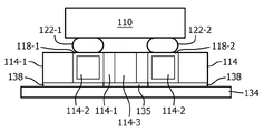
Figure 10 illustrates the LED core 110 being attached on substrate (submount) 114, and it is at US 6,876, is described in further detail in 008.In the upper and lower surface of this substrate can face of weld between electricity be connected to form in this substrate.On its on this substrate top, be furnished with on the bottom that can welding region be connected to this substrate by the conductive path electricity in this substrate of soldered ball 122-1 and 122-2 be attached on solder joint 138 can welding region.Solder joint 138 will can welding region electricity be connected to plate 134 on this base plate bottom.Substrate 114 can be the silicon/glass composite base plate for example with some not same districts.Silicon area 114-2 be metallized thing 118-1 and 118-2 around, described metallide 118-1 and 118-2 form the upper surface of this substrate and the conductive path between lower surface.Circuit such as esd protection circuit can be metallized thing 118-1 and 118-2 around silicon area 114-2 in form, or form in other silicon area 114-3.Other silicon area 114-3 like this can electrically contact with tube core 110 or plate 134 equally.The not same district of glass region 114-1 electric isolation silicon.Solder joint 138 can be by can be for example that the insulation layer 135 of dielectric layer or air is by electric isolation.
In Figure 10, in illustrated device, the substrate 114 that comprises metallide 118-1 and 118-2 was independent of tube core 110 and forms before tube core 110 is attached on substrate 114.For example, US 6,876, and 008 has explained that the Silicon Wafer being comprised of the point for many substrates is grown as the circuit of all esd protection circuits As mentioned above of comprising any hope and so on.Hole forms in this wafer by conventional mask and etch step.Conductive layer such as metal be formed on wafer and hole in.Can be by graphically after this conductive layer.Glassy layer is formed on wafer and hole afterwards.The part of glassy layer and wafer is removed to expose conductive layer.After conductive layer on this wafer downside, can be added with graphical by graphical and additional conductive layer.Once the downside of this wafer is by graphical, independent LED small pieces 110 can 122 physically and be electrically connected to the conduction region on substrate by interconnecting.In other words, LED 100 is labelled to substrate 114 after being cut into independent diode.
Summary of the invention
An object of the present invention is to provide the light emitting semiconductor device that is bonded to support substrates.
The support substrates that embodiments of the invention comprise the through hole that contains main body and a plurality of full depths that extend through this main body.Comprise the light emitting semiconductor device that is clipped in the luminescent layer between HepXing district, N-shaped district and be bonded to this support substrates.This support substrates is not wider than this light emitting semiconductor device.
This light emitting semiconductor device can be bonded to this support substrates in wafer scale technique, so that this device wafers and support substrates are cut into small pieces and therefore this support substrates is not wider than this light emitting semiconductor device simultaneously.Wafer scale technique can be executed at wafer scale to reduce costs by permitting some conventional procedure of processings of carrying out in die-level.
Accompanying drawing explanation
Fig. 1 illustrates a part for light emitting semiconductor device wafer.In Fig. 1, illustrate two luminescent devices.
Fig. 2 illustrates one of device in the Fig. 1 after adding one or more metal levels and one or more polymeric layer.
Fig. 3 illustrates the device that is bonded to support substrates by metal bonding.
Fig. 4 illustrates the device that is bonded to support substrates by single polymeric layer.
Fig. 5 illustrates the device that is bonded to support substrates by being formed on this device and the dielectric layer in this support substrates.
Fig. 6 illustrates the structure that forms the Fig. 3 after through hole in the main body of support substrates.
Fig. 7 illustrates the structure of the Fig. 4 after forming through hole graphical metal and dielectric layer.
Fig. 8 illustrate form additional graphical metal and dielectric layer and attach solder bump and wavelength conversion layer after the structure of Fig. 7.
Fig. 9 illustrates the reflector on the edge that is formed on N-shaped district.
Figure 10 illustrates the prior art device that comprises the LED being arranged on substrate.
Embodiment
In an embodiment of the present invention, light emitting semiconductor device is bonded to pedestal (mount) in wafer scale technique.Although this light emitting semiconductor device is the III group-III nitride LED of transmitting blueness or UV light in example below, but the light emitting semiconductor device such as laser diode except LED and by such as phosphide ,III family of material ,III family of other III-V family arsenide, II-VI family material, ZnO, or the light emitting semiconductor device that other material system of the material based on Si and so on is made also can be used.
Fig. 1 illustrates the part of the wafer of light emitting semiconductor device.In Fig. 1, illustrate two devices.In order to form illustrated structure in Fig. 1, semiconductor structure is grown in growth substrates, and this growth substrates can be any suitable substrate 10 such as for example sapphire, SiC, Si, GaN or compound substrate.This semiconductor structure comprises the luminous or active area 14 being clipped between n HepXing district 12 and 16.Can be first grown and can comprise the multilayer with different component and doping content in N-shaped district 12, this multilayer comprises for example preparation layer such as resilient coating or nucleating layer, and/or be designed to be convenient to that growth substrates removes can be N-shaped or non-layer of having a mind to doping, and be designed for for the particular optical of the hope of luminous zone or electrology characteristic with effective luminous n or p-type device layer even.Luminous or active area 14 is grown in N-shaped district 12.The example of suitable luminous zone comprises single thick or thin luminescent layer, or the multiple quantum well light emitting district that comprises a plurality of thin or thick luminescent layers that separated by barrier layer.P-type district 16 can be grown on luminous zone 14 afterwards.Similar ,pXing district, YunXing district 12 16 can comprise the multilayer with different component, thickness and doping content, and this multilayer comprises non-layer or N-shaped layer of having a mind to doping.In this device, the gross thickness of all semi-conducting materials is less than in certain embodiments 10 μ m and is less than in certain embodiments 6 μ m.First growing p-type district, is then active area, then WeinXing district in certain embodiments.In certain embodiments, semi-conducting material can annealing between 200 ℃ to 800 ℃ alternatively after growth.
Then, be formed on the Metal Contact in p-type district 16.In the device of Fig. 1, p contact comprises two metal levels 18 and 20.Metal 18 can be by for example evaporating or sputter is deposited, afterwards by the standard lithography operations that comprises etching for example or peel off by graphical.Metal 18 can be the reflective metals such as silver for example to obtain the ohmic contact with p-type III group nitride material.Metal 18 can be transition metal and silver-colored multiple-level stack equally.This transition metal can be nickel for example.Metal 18 is 100 to 2000 thick in certain embodiments, is 500 to 1700 thick in certain embodiments, and is 1000 thick to 1600 in certain embodiments.This structure can be annealed for the second time alternatively after the deposition of metal 18.
Optional the 2nd p contacting metal 20 can be on p contacting metal 18 by for example evaporating or sputter is deposited, afterwards by the standard lithography operations such as for example etching or peeling off by graphical.Metal 20 can be the electric conducting material that any minimally reacts with silver, such as the alloy of for example titanium and tungsten.This alloy can or partly, integrally be nitrided or not be nitrided.Metal 20 can be alternatively chromium, platinum or silicon, or can be for optimization is for being attached to peripheral layer and blocking the multiple-level stack of any above-mentioned material of metal 18 diffusion.Metal 20 can be 2000 to 8000 for 1000 to 10000 thick in certain embodiments in certain embodiments, and is 2000 thick to 7000 in certain embodiments.
Lithography operations by standard after this structure is by graphical and be etched by reactive ion etching (RIE) or inductively coupled plasma (ICP) etching (a kind of RIE technique, its applying plasma is produced by RF electromagnetic field) that for example wherein chemical reaction plasma is used to remove semi-conducting material.In certain embodiments, this figure is determined by the mask for graphical p contacting metal 20.In these embodiments, etching can be carried out after etching p contacting metal 20 in single operation.At the full depth in some Zhong,pXing districts, district 16 and the full depth of luminous zone 14, be removed, manifest the surface 13 in N-shaped district 12.NXing district 12 between device in district 11 is etched away afterwards, manifest growth substrates 10, so that III group nitride material is set to leave an edge for 200(resulting devices) distance 202, the distance of the substrate 10 exposing between device is the twice of distance 202.For example, the distance that III group nitride material is set up the edge that leaves device be in certain embodiments 1 μ m between 50 μ m, be less than in certain embodiments 20 μ m, be less than in certain embodiments 10 μ m, and be less than in certain embodiments 6 μ m.
Dielectric 22 can for example be deposited in the structure in Fig. 1 by plasma enhanced chemical vapor deposition (PECVD), chemical vapor deposition (CVD) or evaporation.Dielectric 22 provides electric isolation for being connected to the Metal Contact in nXing HepXing district.The lithography operations of dielectric 22 by standard is by graphical and be etched to expose in 13ZhongnXing district, district 12 and exposed the p contacting metal 20 in district 24 by ICP etching or RIE.Dielectric 22 equally can be by peeling off by graphically.Dielectric 22 can be any suitable dielectric that comprises silicon nitride, silica and silicon oxynitride.In certain embodiments, dielectric 22 is for being optimized to be reflected into the multilayer dielectric stack of the light that is mapped to it.Dielectric 22 in certain embodiments can be thick for being less than 2 μ m, is 200 to 5000 thick in certain embodiments, and be 500 thick to 3200 in certain embodiments.
Shown in Fig. 1, two devices are formed on the wafer of device to illustrate device described herein.For simple and clear object, a device is only shown in Fig. 2,3,4,5,6,7 and 8, although should be understood that a plurality of structures leap wafers shown in these figure and repeat.
In Fig. 2, the metal level 27 and the additional p contact layer 32 that in contact 12 district, N-shaped district, form n contact 26 are deposited with graphical.Metal 27 can be any suitable metal that comprises aluminium or comprise that the multiple layer metal of aluminium, titanium-tungsten alloy, copper and gold is stacking.In the embodiment that metal 27 is multiple-level stack therein, the first metal (i.e. the metal in contiguous N-shaped district 12) can be selected to form to the ohmic contact of GaN reflection blue and white light.Such ground floor can be aluminium for example.Last metal can be to be suitable for for device being attached to the metal of any bonding technology on pedestal.For example, in certain embodiments, bonding technology is that thermocompression bonding and last metal are gold.Metal 27 can be by comprising for example sputter, evaporation, plating or these techniques any suitable technique of combination be deposited.
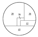
Although in illustrated device, n contact 26 extends beyond the edge in N-shaped district 12 and encounters growth substrates 10 in Fig. 2, in certain embodiments, n contact 26 can be set to leave the edge in N-shaped district 12 so that n contact 26 does not cover the edge in N-shaped district 12.In such embodiments, the polymeric layer 28 of describing hereinafter can be wider, so that it encounters the part that is not covered nXing district 12 by n contact 26.As Fig. 9 of a device part is shown in more illustrated embodiment, reflection dielectric substance 70 is deposited around the edge in N-shaped district 12.Reflection dielectric substance 70 can be the reflection dielectric stack that for example forms with dielectric 22 simultaneously or form in independent deposition and graphical step.Under any circumstance ,nXing district 12 contact with n 26 the two be all set to leave the edge 200 of this device.
After one or more polymeric layers, be deposited with graphical.Polymeric layer 28 is deposited between contiguous device.Polymeric layer 30 by p contact 32 from n contact 26 separately. Polymeric layer 28 and 30 can be same material and can in same operation, be deposited with graphical, although they needn't be done like this.For example, in Fig. 4 in illustrated device, polymeric layer 28 and 30 and bonded layer 42 can be the same material depositing in single step.In this case, the material depositing does not need can not needed by graphical and planarization. Polymeric layer 28 and 30 is resistant to elevated temperatures in certain embodiments.The example of suitable material comprises benzocyclobutane alkenyl polymer, polyimides based polyalcohol, and epoxy resin.In certain embodiments, polymeric layer 28 is doped with the scattering component such as titanium dioxide or the light absorbing material such as carbon black.Polymeric layer 28 can be silicones in certain embodiments.The polymeric layer 28 depositing and 30 can for example be flattened by chemical-mechanical polishing, mechanical polishing or high-speed cutting.
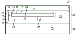
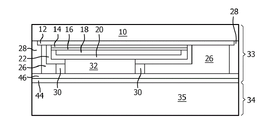
In Fig. 2, the wafer of illustrated device is reversed and is bonded to the wafer of support substrates with respect to illustrated direction in Fig. 2.Between light emitting semiconductor device 33 and support substrates 34, three example view of suitable bonding are in Fig. 3,4 and 5.The support substrates 34 illustrating in Fig. 3,4 and 5 comprises main body 35.Main body can be Si, GaAs or Ge in certain embodiments, or any other suitable material.In certain embodiments, electronic equipment can be integrated in support substrates 34.Integrated element for example can comprise circuit element or the drive electronics for electrostatic discharge (ESD) protection.The example of suitable integrated component comprises diode, resistance and electric capacity.Integrated component can form by conventional semiconductor processing technology.
In Fig. 3, in illustrated structure, optional dielectric 36 is grown in support substrates 34.Dielectric 36 can be the natural oxide (for example silica) of the main body 35 of heat growth, for example, by the dielectric (oxide of silicon, nitride or nitrogen oxide) of PECVD or CVD deposition, or any other suitable dielectric.For example, thermal oxide can be by containing O
2and/or H
2in the gas atmosphere of O, with 800 ℃ to 1200 ℃ heating silicon, grow.PECVD oxide can be at silane and N at 150 ℃ to 400 ℃
2o or O
2, or tetraethyl orthosilicate and N
2o or O
2atmosphere in grow.CVD oxide can be at silane and N at 300 ℃ to 900 ℃
2o or O
2, or tetraethyl orthosilicate and N
2o or O
2atmosphere in grow.
Dielectric 40 is deposited and is graphical.Dielectric 40 provides electricity to be connected to the electric isolation between N-shaped and the metal level of p-type semiconductor layer, so dielectric 40 must be aimed at polymeric layer 30.Dielectric 40 can be polymer or other organic material that is suitable as bonding material or glue.Dielectric 40 can be the combination of for example benzocyclobutane alkenyl polymer, polyimides based polyalcohol, silicon resin base polymer, epoxy resin, material, any other suitable organic material, or inorganic dielectric.Alternatively, the top surface of support substrates 34 (being the top surface of metal 38 and dielectric 40) can, for example by polishing, by chemical-mechanical polishing, or be flattened by any other suitable technique.
In Fig. 4 in illustrated structure, single dielectric bonded layer 42 be formed on the illustrated structure of Fig. 2 top surface (be metal level 26 and 32 and the top surface of polymeric layer 28 and 30) on.Alternatively, dielectric 42 can be formed in the main body 35 of support substrates 34.Dielectric 42 can be polymer or other organic material being suitable for as bonding material or glue.Dielectric 42 can be benzocyclobutane alkenyl polymer, polyimides based polyalcohol, epoxy resin, silicon resin base polymer, or any other suitable organic material.Dielectric 42 can be and polymeric layer 28 and 30 identical materials, although it needs not to be.Dielectric 42 can form by for example spin coating, and can after deposition, for example pass through chemical-mechanical polishing, mechanical polishing, or high-speed cutting is flattened.Dielectric 42 is that in the embodiment of the material identical with polymeric layer 28 and 30, device can for example be flattened by chemical-mechanical polishing in the single step after codeposition therein.In certain embodiments, the planarization of dielectric 42 is optional.Dielectric 42 can be for 100 to 1 μ m are thick on metal level 26 and 32, and to cross over whole wafer be plane.
In Fig. 5 in illustrated device, bonded layer 44 and 46 is respectively formed at main body 35 and device 33 on the two.The bonded layer 46 being formed on device 33 can be the dielectric such as oxide, silicon nitride or the silicon oxynitride of the silicon for example for example depositing by PECVD at low temperatures.For example, PECVD oxide can temperature be 150 ℃ to 400 ℃ at silane and N
2o or O
2, or tetraethyl orthosilicate and N
2o or O
2atmosphere in grow.Dielectric 46 can be thick for 100 to 1 μ m in certain embodiments.The bonded layer 44 being formed in support substrates 34 can be oxide, the silicon nitride such as for example silicon, or the dielectric of silicon oxynitride and so on.The oxide of silicon can be the thermal growth oxide in silicon support substrates, for example by CVD, is at high temperature deposited, or for example by PECVD, be deposited at low temperatures.The thickness of dielectric 44 in certain embodiments can be thick for 100 to 1 μ m.For example, thermal oxide can be by containing O
2and/or H
2in the gas atmosphere of O, at 800 ℃ to 1200 ℃, heating silicon grows.PECVD oxide can temperature be 150 ℃ to 400 ℃ at silane and N
2o or O
2, or tetraethyl orthosilicate and N
2o or O
2atmosphere in grow.CVD oxide can temperature be 300 ℃ to 900 ℃ at silane and N
2o or O
2, or tetraethyl orthosilicate and N
2o or O
2atmosphere in be deposited.
The wafer of device 33 is by a kind of wafer that is bonded to support substrates 34 in illustrated bonding structure in Fig. 3,4 and 5 for example.Bonding can be to carry out between 50 ℃ to 500 ℃ in temperature in certain embodiments, and in temperature, is to carry out between 100 ℃ to 250 ℃ in certain embodiments.Bonding can be carried out under the compression pressure applying lower than 5MPa in certain embodiments.In certain embodiments, after being bonded to the wafer of support substrates 34, growth substrates 10 can remove from device 33 by for example etching or laser lift-off.In the embodiment that growth substrates 10 is removed therein, because the device that there is no a growth substrates is typically too thin to such an extent as to it can not be in self-supporting mechanically, support substrates 34 provides mechanical support for device 33.For example, in Fig. 2, the gross thickness of illustrated device when there is no substrate is not more than 7 μ m in certain embodiments, and is not more than in certain embodiments 25 μ m.Can be by graphical or be roughened for example to improve light by any suitable technique such as Optical Electro-Chemistry etching and extract by removing semi-conducting material that growth substrates 10 exposes.In certain embodiments, growth substrates 10 remains the part of resulting devices.In certain embodiments, growth substrates can for example be shaped by sawing or etching.The main body 35 of support substrates 34, before or after being bonded to device 33, can be thinned to thickness and be 50 μ m in certain embodiments between 250 μ m, and can be thinned in certain embodiments thickness be that 80 μ m are between 120 μ m.Attenuate can be for example carried out by chemico-mechanical polishing or grinding and polishing.
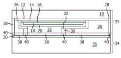
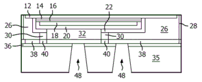
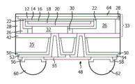
After bonding, through hole forms in support substrates and the structure of bonding stands further processing, as diagram in Fig. 6,7 and 8.Fig. 6 illustrates and is formed on the through hole in illustrated device in Fig. 3.Fig. 7 and 8 illustrates through hole and metal and the dielectric layer being formed on the device illustrating in Fig. 4.In Fig. 6,7 and 8, illustrated processing can be carried out on illustrated device in any Fig. 3,4 and 5.
As shown in Figure 6, through hole 48 is etched through the main body 35 of support substrates 34.Illustrate two through holes, one manifests electricity and is connected to the metal in N-shaped district 12 and one and manifests the metal that electricity is connected to p-type district 16.In Fig. 6 in illustrated device (it comprises illustrated bonding in Fig. 3), through hole 48 is etched through main body 35 and optional dielectric 36 to manifest metal level 38.In Figure 4 and 5, in illustrated device, through hole is etched through bonded layer 42,44 and 46 to manifest p metal 32 and n metal 26.Through hole 48 can for example pass through deep reaction ion etching, reactive ion etching, wet chemical etch, or any other suitable lithographic technique is etched.In the embodiment that support substrates 34 is Si therein, suitable etchant gas comprises for example SF
6and etching can with the deposition time-sharing multiplex that uses the chemical inertness passivation layer on Si sidewall of the octafluorocyclobutane in the technique be for example commonly referred to as Bosch process (Bosch Process).In the embodiment that support substrates 34 is GaAs therein, suitable etchant gas comprises for example Cl
2, HBr or Cl
2mixture with HBr.In the embodiment that support substrates 34 is Ge therein, suitable etchant gas comprises for example Cl
2, SCl
4or Cl
2and SCl
4 mixture.Support substrates 34 is in the embodiment of GaAs or Ge therein, etching equally can with sidewall on the deposition time-sharing multiplex of chemical inertness passivation layer.The sidewall of through hole 48 with respect to main body 35 can be quadrature or be angled as shown in Figure 6.
As shown in Figure 7, after dielectric 50, be deposited on the surface of main body 35 and in through hole 48.Dielectric 50 can be for example the oxide of silicon, the nitrogen oxide of the nitride of silicon or the silicon that for example deposits by PECVD at low temperatures.For example, PECVD oxide can temperature be 150 ℃ to 400 ℃ at silane and N
2o or O
2, or tetraethyl orthosilicate and N
2o or O
2atmosphere in be deposited.Dielectric 50 in certain embodiments can be thick for 100 to 2 μ m.Dielectric 50 subsequently by graphical to expose the metal level 32 and 26 at through hole 48 tops.
Metal level is deposited, and graphically to be formed into p, is connected 52 and 54 with the electricity of n contact afterwards.It can be for example to pass through the Cu of the combined deposition of for example plating, sputter or plating and sputter that electricity connects 52 and 54.Electricity connects 52 and 54 in certain embodiments can be thick and be that 6 μ m are thick to 10 μ m in certain embodiments to 20 μ m for 1 μ m.In cross section as shown in Figure 7, through hole 48 is not connected 52 and 54 by electricity completely and fills.In certain embodiments, the part that through hole 48 is not occupied by dielectric 50 can be connected 52 and 54 by electricity completely and fill.Forming electricity, to connect 52 and 54 metal level can be to comprise that the multiple layer metal of for example Ti, TiW, Cu, Ni and Au the combined deposition by sputter or sputter and plating is stacking.
As shown in Figure 8, dielectric 55 is deposited and graphically for electric isolation and/or protection electricity, is connected 52 and 54.Dielectric 55 can be for example one or more benzocyclobutane alkenyl polymers or one or more polyimides based polyalcohols.Through hole 48 is not also formed electricity and connects in the embodiment that 52 and 54 metal level fills completely therein, and dielectric 55 can be arranged to mainly or filling vias 48 fully, or through hole 48 can be held not fill.
Alternatively, after additional metal level, be deposited to form scolder and connect 56 and 58.Additional metal can be any be suitable as electricity connect 52 and 54 and interconnect 60 and 62(be solder bump in certain embodiments) between the metal of connection.For scolder, connect NiV or the ground floor of Ni of plating and the second thin layer of the Au of sputter afterwards or plating that the example of 56 and 58 suitable construction comprises sputter, the 3rd thin layer of the Au of the second layer of the NiV of the ground floor of the TiW of sputter and sputter afterwards or the Ni of plating and sputter afterwards or plating, or the second layer of the Cu of the ground floor of the TiW of sputter or plating and plating afterwards and the Au of sputter afterwards or plating the 3rd layer.Scolder connects 56 and 58 can have 1 μ m in certain embodiments to the gross thickness of 15 μ m.
In certain embodiments, wavelength conversion layer 64 is disposed on luminescent layer 14 and in the path of the light of launching at this luminescent layer.Wavelength conversion layer 64 can separate with device, if growth substrates 10 has been removed, is labelled to N-shaped district 12, if existed, is labelled to growth substrates 10.Wavelength conversion layer comprises one or more and is arranged to the light that absorbs luminescent layer transmitting the light wavelength transition material of launching different wave length.All or only a part by luminescent layer, launched and the light that incides on wavelength conversion layer can be changed by material for transformation of wave length.The non-switched light of being launched by luminescent layer can be a part for the final spectrum of light, although it needs not to be.The example of common combination comprises the blue emission LED with the combination of yellow emission material for transformation of wave length, blue emission LED with green glow and the combination of red emission material for transformation of wave length, with the UV transmitting LED of blue light and the combination of yellow emission material for transformation of wave length, and launch LED with the UV of blue light, green glow and the combination of red emission material for transformation of wave length.The material for transformation of wave length of launching other color of light can be added to customize transmitting from the spectrum of the light of this device.
In certain embodiments, wavelength conversion layer 64 is only material for transformation of wave length in device.In certain embodiments, wavelength conversion layer 64 combines with other Wavelength changing element such as other phosphor, quantum dot, semiconductor Wavelength changing element or dyestuff, to create the monochromatic light of white light or other color.
In certain embodiments, being suitable for that the structure shown in Fig. 8 is attached to another structural optional interconnection 60 and 62 such as printed circuit board (PCB) is formed on and is connected on 56 and 58. Interconnection 60 and 62 is generally solder bump but any suitable interconnection can be used.Solder bump 60 and 62 can be the alloy (SAC scolder) of for example tin, silver and copper or the alloy of Jin Hexi.This scolder can apply by comprising any suitable technology of for example electroplating.After plating, this structure can be refluxed to make the micro-structural of this structure and solder bump 60 and 62 level and smooth subsequently.
Afterwards, the wafer that is bonded to the device 33 of support substrates 34 can be cut into independent luminescent device chip.Due to device 33 and support substrates 34 by together with cut into pieces, support substrates is not wider than device, as shown in Fig. 3,4,5,6,7 and 8.Simple grainization can be for example by conventional sawing, laser ablation by the light with 193nm, 248nm or 355nm or spray cutting by water and carry out.Simple grainization can be performed via the combination of scribing and mechanical breaking equally, and wherein scribing is for example by conventional sawing, laser ablation by the light with 193nm, 248nm or 355nm or spray cutting by water and carry out.
Because above-mentioned device is bonded to support substrates in wafer scale, embodiments of the invention can provide than device wherein and be bonded to one by one efficiency that the conventional scheme of support substrates is higher and the reduction of cost tube core.For example, possibility due to the wafer scale processing of the LED by many process operations that are typically executed at package level in conventional LED, therefore efficiency can promote, and wherein said process operation comprises the removing of growth substrates, roughening that growth substrates removes semiconductor surfaces following and forms wavelength conversion layer.
In the vertical Integrated Solution of conventional semiconductor, the device being integrated is same material or the material with similar thermal coefficient of expansion (CTE) often on paper.Like this, the wafer bonding of this structure can be carried out at the temperature improving.In III nitride devices, be grown on sapphire and wafer bonding to silicon support substrates wafer in the situation that, the CTE of sapphire and silicon is enough different, to such an extent as to wafer bonding at the temperature improving can cause being locked in the significant stress in this bonding structure, cause the crooked and broken of between processing period subsequently this bonding structure.In some the above embodiments, this device is bonded to support substrates at low temperatures, and this can cause in this structure the minimum stress of locking, and this can improve output.For example, be bonded in certain embodiments lower than carrying out at 300 ℃ in certain embodiments between 230 ℃ to 275 ℃ or carry out under lower temperature.At some, use in the embodiment of silicon resin base bonded layer, bonding can be carried out at lower than 150 ℃.
In certain embodiments, because support substrates wafer does not comprise any feature when the bonding, so the wafer of device just can be bonded to support substrates wafer without complicated aligning.This device and support substrates wafer only need to aim at roughly, for example, by vision, aim at, and still do not require the accurate aligning of patterned features on two wafers.After bonding, via etch mask has to aim at LED metallide, and this can aim at by IR (wafer that sees through bonding is observed) or aim at (mask in support substrates wafer side is aimed at the view of the LED figure of seeing as the transparent growth substrates seeing through such as sapphire) behind and be performed.
Described the present invention in detail, those skilled in the art will appreciate that given present disclosure, can modify and not depart from the spirit in creative concept described herein the present invention.Therefore, be not intended to limit the scope of the present invention to the specific embodiment of diagram and description.
Claims (15)
1. a structure, comprising:
Support substrates, comprises main body and a plurality of through hole that extends through the full depth of described main body; And
Light emitting semiconductor device, comprises the luminescent layer being clipped between HepXing district, N-shaped district, and wherein this light emitting semiconductor device is bonded to this support substrates;
Wherein this support substrates is not wider than this light emitting semiconductor device.
2. structure according to claim 1, wherein GainXing district is set to leave the edge of this light emitting semiconductor device.
3. structure according to claim 2, further comprises the polymeric layer being arranged between the edge in GainXing district and the edge of this light emitting semiconductor device.
4. structure according to claim 1, further comprises the Metal Contact being arranged in GainXing district.
5. structure according to claim 4, wherein this Metal Contact extends beyond the sidewall on the edge in GainXing district.
6. structure according to claim 4, wherein:
This Metal Contact is set to leave the edge in GainXing district; And
Reflection dielectric medium structure is disposed on the outside and sidewall in GainXing district.
7. structure according to claim 1, wherein this light emitting semiconductor device is bonded to this support substrates via the bonded layer that comprises a plurality of metal areas that separated by least one dielectric region.
8. structure according to claim 7, the plurality of through hole that wherein extends through the full depth of this main body exposes the plurality of metal area.
9. structure according to claim 1, wherein this light emitting semiconductor device is bonded to this support substrates via the bonded layer that comprises polymer.
10. structure according to claim 9, the plurality of through hole that wherein extends through the full depth of this main body extends through this polymer-bound layer and arrives the metal level on this light emitting semiconductor device.
11. structures according to claim 1, wherein this light emitting semiconductor device is bonded to this support substrates via the second bonded layer that is formed on the first bonded layer on this light emitting semiconductor device and be formed in this support substrates.
12. structures according to claim 11, wherein this first and second bonded layer is dielectric layer.
13. structures according to claim 11, wherein at least one in this first and second bonded layer comprises the oxide of silicon.
14. structures according to claim 11, the plurality of through hole that wherein extends through the full depth of this main body extend through this first and second bonded layer the two to expose the metal level on this light emitting semiconductor device.
15. structures according to claim 1, further comprise the wavelength conversion layer being disposed on this light emitting semiconductor device.
Priority Applications (1)
| Application Number | Priority Date | Filing Date | Title |
|---|---|---|---|
| CN202010107160.1A CN111509103A (en) | 2011-06-01 | 2012-05-22 | Light emitting device bonded to a support substrate |
Applications Claiming Priority (3)
| Application Number | Priority Date | Filing Date | Title |
|---|---|---|---|
| US201161491920P | 2011-06-01 | 2011-06-01 | |
| US61/491,920 | 2011-06-01 | ||
| PCT/IB2012/052556 WO2012164437A2 (en) | 2011-06-01 | 2012-05-22 | Light emitting device bonded to a support substrate |
Related Child Applications (1)
| Application Number | Title | Priority Date | Filing Date |
|---|---|---|---|
| CN202010107160.1A Division CN111509103A (en) | 2011-06-01 | 2012-05-22 | Light emitting device bonded to a support substrate |
Publications (1)
| Publication Number | Publication Date |
|---|---|
| CN103563099A true CN103563099A (en) | 2014-02-05 |
Family
ID=46331645
Family Applications (2)
| Application Number | Title | Priority Date | Filing Date |
|---|---|---|---|
| CN201280026289.3A Pending CN103563099A (en) | 2011-06-01 | 2012-05-22 | Light emitting device bonded to a support substrate |
| CN202010107160.1A Pending CN111509103A (en) | 2011-06-01 | 2012-05-22 | Light emitting device bonded to a support substrate |
Family Applications After (1)
| Application Number | Title | Priority Date | Filing Date |
|---|---|---|---|
| CN202010107160.1A Pending CN111509103A (en) | 2011-06-01 | 2012-05-22 | Light emitting device bonded to a support substrate |
Country Status (8)
| Country | Link |
|---|---|
| US (1) | US20140077246A1 (en) |
| EP (1) | EP2715807B8 (en) |
| JP (3) | JP2014515560A (en) |
| KR (1) | KR20140034262A (en) |
| CN (2) | CN103563099A (en) |
| RU (1) | RU2604956C2 (en) |
| TW (1) | TWI617055B (en) |
| WO (1) | WO2012164437A2 (en) |
Cited By (1)
| Publication number | Priority date | Publication date | Assignee | Title |
|---|---|---|---|---|
| CN107980183A (en) * | 2015-08-12 | 2018-05-01 | 欧司朗光电半导体有限公司 | Semiconductor chip |
Families Citing this family (16)
| Publication number | Priority date | Publication date | Assignee | Title |
|---|---|---|---|---|
| JP6062429B2 (en) | 2011-07-15 | 2017-01-18 | コーニンクレッカ フィリップス エヌ ヴェKoninklijke Philips N.V. | Method for bonding a semiconductor device to a support substrate |
| US20140209961A1 (en) * | 2013-01-30 | 2014-07-31 | Luxo-Led Co., Limited | Alternating current light emitting diode flip-chip |
| WO2015008189A2 (en) * | 2013-07-18 | 2015-01-22 | Koninklijke Philips N.V. | Dicing a wafer of light emitting devices |
| JP6256026B2 (en) * | 2014-01-17 | 2018-01-10 | 日亜化学工業株式会社 | LIGHT EMITTING DEVICE AND LIGHT EMITTING DEVICE MANUFACTURING METHOD |
| DE102014116141B4 (en) * | 2014-11-05 | 2022-07-28 | OSRAM Opto Semiconductors Gesellschaft mit beschränkter Haftung | Method for producing at least one optoelectronic semiconductor chip, optoelectronic semiconductor chip and optoelectronic semiconductor component |
| FR3033939B1 (en) * | 2015-03-20 | 2018-04-27 | Commissariat A L'energie Atomique Et Aux Energies Alternatives | OPTOELECTRONIC DEVICE WITH ELECTROLUMINESCENT DIODE |
| KR102441311B1 (en) * | 2015-04-20 | 2022-09-08 | 쑤저우 레킨 세미컨덕터 컴퍼니 리미티드 | Light Emitting Device |
| DE102016113193A1 (en) * | 2016-07-18 | 2018-01-18 | Osram Opto Semiconductors Gmbh | Component with geometrically adapted contact structure and its manufacturing method |
| US10186478B2 (en) | 2016-12-30 | 2019-01-22 | Texas Instruments Incorporated | Packaged semiconductor device with a particle roughened surface |
| KR102378919B1 (en) * | 2017-08-03 | 2022-03-28 | 루미레즈 엘엘씨 | Method of manufacturing a light emitting device |
| TWI642335B (en) * | 2017-12-11 | 2018-11-21 | 欣興電子股份有限公司 | Circuit board and manufacturing method thereof |
| EP3528296B1 (en) * | 2018-02-16 | 2020-06-03 | Nichia Corporation | Light emitting element and light emitting device |
| US10374386B1 (en) * | 2018-06-07 | 2019-08-06 | Finisar Corporation | Chip on carrier |
| JP7385111B2 (en) | 2019-09-26 | 2023-11-22 | 日亜化学工業株式会社 | Manufacturing method of light emitting device and light emitting device |
| RU195271U1 (en) * | 2019-11-25 | 2020-01-21 | федеральное государственное бюджетное образовательное учреждение высшего образования "Новгородский государственный университет имени Ярослава Мудрого" | ARSENID-GALLIUM MAGNETOELECTRIC DIODE |
| KR102552204B1 (en) | 2022-11-08 | 2023-07-06 | 박영우 | Under water imaging system using LED |
Citations (6)
| Publication number | Priority date | Publication date | Assignee | Title |
|---|---|---|---|---|
| CN1121090A (en) * | 1994-04-05 | 1996-04-24 | 摩托罗拉公司 | Method of adhesion to a polymide surface by formation of covalent bonds |
| US20070096130A1 (en) * | 2005-06-09 | 2007-05-03 | Philips Lumileds Lighting Company, Llc | LED Assembly Having Maximum Metal Support for Laser Lift-Off of Growth Substrate |
| CN101097855A (en) * | 2006-06-28 | 2008-01-02 | 财团法人工业技术研究院 | Fabrication process of nitride semiconductor substrate and composite material substrate |
| CN101512783A (en) * | 2006-05-02 | 2009-08-19 | 三菱化学株式会社 | Semiconductor light-emitting element |
| US20100025713A1 (en) * | 2008-08-01 | 2010-02-04 | Tao Chin-San | Wafer-scaled light-emitting structure |
| JP2010103186A (en) * | 2008-10-21 | 2010-05-06 | Sony Corp | Method of manufacturing semiconductor light emitting apparatus |
Family Cites Families (28)
| Publication number | Priority date | Publication date | Assignee | Title |
|---|---|---|---|---|
| WO1998054764A1 (en) * | 1997-05-27 | 1998-12-03 | Osram Opto Semiconductors Gmbh & Co. Ohg | Method for producing a light-emitting component |
| US6455878B1 (en) * | 2001-05-15 | 2002-09-24 | Lumileds Lighting U.S., Llc | Semiconductor LED flip-chip having low refractive index underfill |
| JP4447806B2 (en) * | 2001-09-26 | 2010-04-07 | スタンレー電気株式会社 | Light emitting device |
| JP4214704B2 (en) * | 2002-03-20 | 2009-01-28 | 日亜化学工業株式会社 | Semiconductor element |
| JP3962282B2 (en) * | 2002-05-23 | 2007-08-22 | 松下電器産業株式会社 | Manufacturing method of semiconductor device |
| JP4123830B2 (en) * | 2002-05-28 | 2008-07-23 | 松下電工株式会社 | LED chip |
| US6876008B2 (en) | 2003-07-31 | 2005-04-05 | Lumileds Lighting U.S., Llc | Mount for semiconductor light emitting device |
| TWI246783B (en) * | 2003-09-24 | 2006-01-01 | Matsushita Electric Works Ltd | Light-emitting device and its manufacturing method |
| CN101032034A (en) * | 2004-06-30 | 2007-09-05 | 克里公司 | Chip-scale methods for packaging light emitting devices and chip-scale packaged light emitting devices |
| US9368428B2 (en) * | 2004-06-30 | 2016-06-14 | Cree, Inc. | Dielectric wafer level bonding with conductive feed-throughs for electrical connection and thermal management |
| JP4535834B2 (en) * | 2004-10-18 | 2010-09-01 | パナソニック電工株式会社 | Light emitting device and manufacturing method thereof |
| TWI244228B (en) * | 2005-02-03 | 2005-11-21 | United Epitaxy Co Ltd | Light emitting device and manufacture method thereof |
| US7335924B2 (en) * | 2005-07-12 | 2008-02-26 | Visual Photonics Epitaxy Co., Ltd. | High-brightness light emitting diode having reflective layer |
| JP2006279080A (en) * | 2006-07-10 | 2006-10-12 | Sanyo Electric Co Ltd | Fixing method for light emitting element wafer |
| JP2009105123A (en) * | 2007-10-22 | 2009-05-14 | Showa Denko Kk | Light-emitting diode, and manufacturing method thereof |
| US8878219B2 (en) * | 2008-01-11 | 2014-11-04 | Cree, Inc. | Flip-chip phosphor coating method and devices fabricated utilizing method |
| TW201010122A (en) * | 2008-08-21 | 2010-03-01 | Univ Nat Central | Flip-chip light-emitting diode having the epitaxy strengthening layer, and fabrication method thereof |
| US9117944B2 (en) * | 2008-09-24 | 2015-08-25 | Koninklijke Philips N.V. | Semiconductor light emitting devices grown on composite substrates |
| JP4724222B2 (en) * | 2008-12-12 | 2011-07-13 | 株式会社東芝 | Method for manufacturing light emitting device |
| JP5518502B2 (en) * | 2009-01-27 | 2014-06-11 | シチズン電子株式会社 | Manufacturing method of light emitting diode |
| KR101007130B1 (en) * | 2009-02-18 | 2011-01-10 | 엘지이노텍 주식회사 | Light emitting device and method for fabricating the same |
| JP4871973B2 (en) * | 2009-04-28 | 2012-02-08 | 株式会社沖データ | Semiconductor thin film element manufacturing method, semiconductor wafer, and semiconductor thin film element |
| JP4686625B2 (en) * | 2009-08-03 | 2011-05-25 | 株式会社東芝 | Manufacturing method of semiconductor light emitting device |
| JP2011071272A (en) * | 2009-09-25 | 2011-04-07 | Toshiba Corp | Semiconductor light-emitting device and method for manufacturing the same |
| JP5534763B2 (en) * | 2009-09-25 | 2014-07-02 | 株式会社東芝 | Semiconductor light emitting device manufacturing method and semiconductor light emitting device |
| JP5378130B2 (en) * | 2009-09-25 | 2013-12-25 | 株式会社東芝 | Semiconductor light emitting device |
| TWI505428B (en) * | 2010-03-11 | 2015-10-21 | Xintec Inc | Chip package and method for forming the same |
| KR101762173B1 (en) * | 2011-01-13 | 2017-08-04 | 삼성전자 주식회사 | Wafer level light emitting device package and method of manufacturing the same |
-
2012
- 2012-05-22 EP EP12729222.5A patent/EP2715807B8/en active Active
- 2012-05-22 JP JP2014513278A patent/JP2014515560A/en active Pending
- 2012-05-22 CN CN201280026289.3A patent/CN103563099A/en active Pending
- 2012-05-22 KR KR1020137034940A patent/KR20140034262A/en not_active Application Discontinuation
- 2012-05-22 RU RU2013158689/28A patent/RU2604956C2/en not_active IP Right Cessation
- 2012-05-22 US US14/114,809 patent/US20140077246A1/en not_active Abandoned
- 2012-05-22 WO PCT/IB2012/052556 patent/WO2012164437A2/en active Application Filing
- 2012-05-22 CN CN202010107160.1A patent/CN111509103A/en active Pending
- 2012-05-29 TW TW101119205A patent/TWI617055B/en active
-
2017
- 2017-02-08 JP JP2017021056A patent/JP2017108156A/en active Pending
-
2019
- 2019-03-19 JP JP2019051248A patent/JP2019114804A/en active Pending
Patent Citations (6)
| Publication number | Priority date | Publication date | Assignee | Title |
|---|---|---|---|---|
| CN1121090A (en) * | 1994-04-05 | 1996-04-24 | 摩托罗拉公司 | Method of adhesion to a polymide surface by formation of covalent bonds |
| US20070096130A1 (en) * | 2005-06-09 | 2007-05-03 | Philips Lumileds Lighting Company, Llc | LED Assembly Having Maximum Metal Support for Laser Lift-Off of Growth Substrate |
| CN101512783A (en) * | 2006-05-02 | 2009-08-19 | 三菱化学株式会社 | Semiconductor light-emitting element |
| CN101097855A (en) * | 2006-06-28 | 2008-01-02 | 财团法人工业技术研究院 | Fabrication process of nitride semiconductor substrate and composite material substrate |
| US20100025713A1 (en) * | 2008-08-01 | 2010-02-04 | Tao Chin-San | Wafer-scaled light-emitting structure |
| JP2010103186A (en) * | 2008-10-21 | 2010-05-06 | Sony Corp | Method of manufacturing semiconductor light emitting apparatus |
Cited By (2)
| Publication number | Priority date | Publication date | Assignee | Title |
|---|---|---|---|---|
| CN107980183A (en) * | 2015-08-12 | 2018-05-01 | 欧司朗光电半导体有限公司 | Semiconductor chip |
| CN107980183B (en) * | 2015-08-12 | 2020-03-03 | 欧司朗光电半导体有限公司 | Semiconductor chip |
Also Published As
| Publication number | Publication date |
|---|---|
| WO2012164437A2 (en) | 2012-12-06 |
| EP2715807B1 (en) | 2018-05-16 |
| KR20140034262A (en) | 2014-03-19 |
| RU2604956C2 (en) | 2016-12-20 |
| JP2019114804A (en) | 2019-07-11 |
| RU2013158689A (en) | 2015-07-20 |
| EP2715807B8 (en) | 2018-10-24 |
| WO2012164437A3 (en) | 2013-01-17 |
| TWI617055B (en) | 2018-03-01 |
| CN111509103A (en) | 2020-08-07 |
| JP2014515560A (en) | 2014-06-30 |
| JP2017108156A (en) | 2017-06-15 |
| US20140077246A1 (en) | 2014-03-20 |
| EP2715807A2 (en) | 2014-04-09 |
| TW201306322A (en) | 2013-02-01 |
Similar Documents
| Publication | Publication Date | Title |
|---|---|---|
| JP6712579B2 (en) | Method of mounting light emitting device on supporting substrate | |
| CN103563099A (en) | Light emitting device bonded to a support substrate | |
| US11721788B2 (en) | Method of bonding a semiconductor device to a support substrate | |
| US20180323353A1 (en) | Sealed semiconductor light emitting device | |
| WO2012164456A1 (en) | Method of attaching a light emitting device to a support substrate |
Legal Events
| Date | Code | Title | Description |
|---|---|---|---|
| C06 | Publication | ||
| PB01 | Publication | ||
| C10 | Entry into substantive examination | ||
| SE01 | Entry into force of request for substantive examination | ||
| TA01 | Transfer of patent application right | ||
| TA01 | Transfer of patent application right |
Effective date of registration: 20180326 Address after: Holland Schiphol Applicant after: LUMILEDS HOLDING B.V. Address before: Holland Ian Deho Finn Applicant before: Koninkl Philips Electronics NV |
|
| RJ01 | Rejection of invention patent application after publication | ||
| RJ01 | Rejection of invention patent application after publication |
Application publication date: 20140205 |