EP2190185A1 - Festkörperabbildungselement - Google Patents
Festkörperabbildungselement Download PDFInfo
- Publication number
- EP2190185A1 EP2190185A1 EP08829399A EP08829399A EP2190185A1 EP 2190185 A1 EP2190185 A1 EP 2190185A1 EP 08829399 A EP08829399 A EP 08829399A EP 08829399 A EP08829399 A EP 08829399A EP 2190185 A1 EP2190185 A1 EP 2190185A1
- Authority
- EP
- European Patent Office
- Prior art keywords
- pixel
- memory
- area
- solid
- image sensor
- Prior art date
- Legal status (The legal status is an assumption and is not a legal conclusion. Google has not performed a legal analysis and makes no representation as to the accuracy of the status listed.)
- Granted
Links
- 238000003384 imaging method Methods 0.000 title abstract description 38
- 239000007787 solid Substances 0.000 title 1
- 238000003860 storage Methods 0.000 claims abstract description 98
- 239000003990 capacitor Substances 0.000 claims abstract description 66
- 239000004065 semiconductor Substances 0.000 claims abstract description 31
- 239000000758 substrate Substances 0.000 claims abstract description 7
- 238000006243 chemical reaction Methods 0.000 claims description 51
- 238000012546 transfer Methods 0.000 claims description 38
- 238000000034 method Methods 0.000 claims description 34
- 238000001514 detection method Methods 0.000 claims description 31
- 230000008569 process Effects 0.000 claims description 24
- 230000015572 biosynthetic process Effects 0.000 claims description 2
- 230000006866 deterioration Effects 0.000 abstract description 4
- 238000000926 separation method Methods 0.000 abstract description 4
- 238000009792 diffusion process Methods 0.000 description 74
- 238000005070 sampling Methods 0.000 description 22
- 238000010586 diagram Methods 0.000 description 16
- 238000001444 catalytic combustion detection Methods 0.000 description 11
- 238000011065 in-situ storage Methods 0.000 description 6
- 229920006395 saturated elastomer Polymers 0.000 description 6
- 230000035945 sensitivity Effects 0.000 description 4
- XUIMIQQOPSSXEZ-UHFFFAOYSA-N Silicon Chemical compound [Si] XUIMIQQOPSSXEZ-UHFFFAOYSA-N 0.000 description 3
- XAGFODPZIPBFFR-UHFFFAOYSA-N aluminium Chemical compound [Al] XAGFODPZIPBFFR-UHFFFAOYSA-N 0.000 description 3
- 230000007423 decrease Effects 0.000 description 3
- 229910021420 polycrystalline silicon Inorganic materials 0.000 description 3
- 229920005591 polysilicon Polymers 0.000 description 3
- 229910052710 silicon Inorganic materials 0.000 description 3
- 239000010703 silicon Substances 0.000 description 3
- 102100024020 Guanine nucleotide-binding protein-like 1 Human genes 0.000 description 2
- 101000904099 Homo sapiens Guanine nucleotide-binding protein-like 1 Proteins 0.000 description 2
- 241000709701 Human poliovirus 1 Species 0.000 description 2
- 230000003213 activating effect Effects 0.000 description 2
- 229910052782 aluminium Inorganic materials 0.000 description 2
- 238000002485 combustion reaction Methods 0.000 description 2
- 230000006378 damage Effects 0.000 description 2
- 238000013461 design Methods 0.000 description 2
- 230000000694 effects Effects 0.000 description 2
- 238000004880 explosion Methods 0.000 description 2
- 230000006870 function Effects 0.000 description 2
- 239000012535 impurity Substances 0.000 description 2
- 229910052751 metal Inorganic materials 0.000 description 2
- 239000002184 metal Substances 0.000 description 2
- 230000003071 parasitic effect Effects 0.000 description 2
- 238000001454 recorded image Methods 0.000 description 2
- 101100372602 Arabidopsis thaliana VDAC3 gene Proteins 0.000 description 1
- 101100428768 Arabidopsis thaliana VSR1 gene Proteins 0.000 description 1
- 101100428770 Arabidopsis thaliana VSR2 gene Proteins 0.000 description 1
- 206010034960 Photophobia Diseases 0.000 description 1
- 241000512294 Thais Species 0.000 description 1
- 206010047571 Visual impairment Diseases 0.000 description 1
- 238000009825 accumulation Methods 0.000 description 1
- 230000009286 beneficial effect Effects 0.000 description 1
- 230000008859 change Effects 0.000 description 1
- 125000004122 cyclic group Chemical group 0.000 description 1
- 230000003247 decreasing effect Effects 0.000 description 1
- 238000011161 development Methods 0.000 description 1
- 238000007599 discharging Methods 0.000 description 1
- 230000005284 excitation Effects 0.000 description 1
- 230000020169 heat generation Effects 0.000 description 1
- 238000002347 injection Methods 0.000 description 1
- 239000007924 injection Substances 0.000 description 1
- 208000013469 light sensitivity Diseases 0.000 description 1
- 238000004519 manufacturing process Methods 0.000 description 1
- 238000012986 modification Methods 0.000 description 1
- 230000004048 modification Effects 0.000 description 1
- 238000000059 patterning Methods 0.000 description 1
- 238000005036 potential barrier Methods 0.000 description 1
- 238000012545 processing Methods 0.000 description 1
- 230000005855 radiation Effects 0.000 description 1
- 230000009467 reduction Effects 0.000 description 1
- 238000012552 review Methods 0.000 description 1
- 238000013519 translation Methods 0.000 description 1
Images


Classifications
-
- H—ELECTRICITY
- H04—ELECTRIC COMMUNICATION TECHNIQUE
- H04N—PICTORIAL COMMUNICATION, e.g. TELEVISION
- H04N25/00—Circuitry of solid-state image sensors [SSIS]; Control thereof
- H04N25/50—Control of the SSIS exposure
- H04N25/57—Control of the dynamic range
- H04N25/571—Control of the dynamic range involving a non-linear response
- H04N25/575—Control of the dynamic range involving a non-linear response with a response composed of multiple slopes
-
- H—ELECTRICITY
- H04—ELECTRIC COMMUNICATION TECHNIQUE
- H04N—PICTORIAL COMMUNICATION, e.g. TELEVISION
- H04N25/00—Circuitry of solid-state image sensors [SSIS]; Control thereof
- H04N25/70—SSIS architectures; Circuits associated therewith
- H04N25/71—Charge-coupled device [CCD] sensors; Charge-transfer registers specially adapted for CCD sensors
- H04N25/75—Circuitry for providing, modifying or processing image signals from the pixel array
-
- H—ELECTRICITY
- H04—ELECTRIC COMMUNICATION TECHNIQUE
- H04N—PICTORIAL COMMUNICATION, e.g. TELEVISION
- H04N25/00—Circuitry of solid-state image sensors [SSIS]; Control thereof
- H04N25/70—SSIS architectures; Circuits associated therewith
- H04N25/76—Addressed sensors, e.g. MOS or CMOS sensors
- H04N25/77—Pixel circuitry, e.g. memories, A/D converters, pixel amplifiers, shared circuits or shared components
- H04N25/771—Pixel circuitry, e.g. memories, A/D converters, pixel amplifiers, shared circuits or shared components comprising storage means other than floating diffusion
-
- H—ELECTRICITY
- H04—ELECTRIC COMMUNICATION TECHNIQUE
- H04N—PICTORIAL COMMUNICATION, e.g. TELEVISION
- H04N25/00—Circuitry of solid-state image sensors [SSIS]; Control thereof
- H04N25/70—SSIS architectures; Circuits associated therewith
- H04N25/76—Addressed sensors, e.g. MOS or CMOS sensors
- H04N25/78—Readout circuits for addressed sensors, e.g. output amplifiers or A/D converters
Definitions
- the present invention relates to a solid-state image sensor and, more specifically, to a solid-state image sensor capable of high-speed operations suitable for taking images of high-speed phenomena such as destructions, explosions and combustions.
- High-speed imaging devices for taking consecutive images of high-speed phenomena such as explosions, destructions, combustions, collisions and discharges for only a short period of time have been conventionally developed (for example, refer to Non-Patent Document 1 and other documents).
- Such high-speed imaging devices need to perform an ultrahigh-speed imaging operation that exceeds a level of approximately one million images per second. Accordingly, they use solid-state image sensors capable of high-speed operations, which have special structures different from those of the imaging devices used in normal video cameras, digital cameras and similar devices.
- Patent Document I One example of this type of solid-state image sensor is disclosed in Patent Document I and other documents, which is referred to as an in-situ storage image sensor.
- An outline of this image sensor is as follows: A storage CCD, which also serves for the transfer of a specified number of recorded images (frames), is provided for each photodiode as a photo-receiver. During an imaging operation, pixel signals resulting from photoelectric conversion by the photodiode are sequentially transferred to the storage CCD. After the imaging operation is completed, the pixel signals corresponding to the specified number of images stored in the storage CCD are collectively read, and the specified number of recorded images are reproduced outside the image sensor. During the imaging operation, pixel signals exceeding the specified number of images are discarded from the oldest ones.
- the latest set of pixel signals corresponding to the specified number of images are held in the storage CCD. This means that, when the transfer of pixel signals to the storage CCD is suspended at the completion of the imaging operation, one can obtain the latest series of images ranging from the completion of the imaging operation back through a period of time corresponding to the specified number of images.
- the in-situ storage image sensor is characterized by its capability of acquiring a plurality of consecutive images at extremely high speeds.
- the in-situ storage image sensor has the hollowing problems.
- the aforementioned in-situ storage image sensor inherently consumes a large amount of power. This is because the gate electrodes and signal lines, both having high capacitive loads, must be simultaneously driven during the process of transferring signal charges to the CCD, and also because the voltage amplitude of the gate-driving signal is large. Attempting to increase the drive speed for higher imaging speeds would additionally increase the power consumption and possibly cause heat generation that exceeds the upper limit of heat radiation. Furthermore, the high capacitive load may cause waveform distortion of the drive signal (e.g. unsharpening of the waveform), in which case the attempt of increasing the imaging speed may totally prevent the charge transfer.
- Patent Document 2 a device disclosed in Patent Document 2 has been known.
- this image sensor a plurality of capacitors acting as memory elements are provided within each pixel so that the photocharges produced by the photodiode can be consecutively stored, for each frame, in a different set of memory capacitors.
- this device can continuously record a few to several frames, it cannot perform the continuous imaging operation over such a large number of frames that the aforementioned high-speed imaging device is intended for.
- Using more memory capacitors to increase the number of continuously recordable frames results in a higher capacitive load of the signal lines extending from the detection node storing the charges produced by the photodiode, which makes it difficult to raise the operation speed.
- the area of the photodiode within each pixel inevitably decreases, which lowers the aperture ratio and accordingly deteriorates the sensitivity.
- the present invention has been developed in view of these problems, and its main objective is to provide a solid-state image sensor capable of performing continuous imaging operations at extremely high speeds yet with low power consumption. Another objective of the present invention is to provide a solid-state image sensor in which the image quality is enhanced by improving the S/N ratio and/or dynamic range of the pixel signals obtained by a continuous high-speed imaging operation.
- the solid-state image sensor according to the first aspect of the present invention has a CMOS structure.
- the photoelectric conversion element may be, for example, a photodiode, and more preferably an embedded photodiode.
- the memory section may use a capacitor to hold output signals from each pixel.
- a pixel output line independently extends from each pixel within the pixel area to the memory area, and the plurality of memory sections are respectively connected to the pixel output lines. Therefore, the signals corresponding to the charges obtained by storing photocharges produced by the photoelectric conversion elements of the pixels can be sequentially transferred through the pixel output lines, which are respectively provided for each pixel, to be held in the memory sections.
- the solid-state image sensor according to the first aspect of the present invention includes a plurality of memory sections respectively corresponding to the pixels, it is unnecessary to simultaneously drive all the gate loads in the process of holding new signal charges as in the case of the conventional in-situ storage image sensor using a storage CCD. Accordingly, it has low power consumption and generates less heat even when driven at high speeds. Its low capacitive load reduces the magnitude of distortion of the drive waveform even during the high-speed driving, thus enabling signals to be assuredly extracted from the pixels to the memory sections.
- the number of memory sections corresponding to one pixel can be increased without affecting the other design factors, e.g. the number of pixels within the pixel area, the area of the light-receiving surface of the photoelectric conversion element, and the overall size of the pixel area. Accordingly, it is possible to provide an adequately large number of frames for continuous high-speed imaging operations.
- the plurality of memory sections may each include at least one memory element and has a gate means provided between each memory element and the pixel output line.
- each pixel within the pixel area may include: a transfer element for transferring the photocharges produced by the photoelectric conversion element to a detection node for converting electric charge signals to voltage signals; a buffer element, provided between the defection node and the pixel output line of each pixel, for sending signals from the detection node to the pixel output line; and a reset element for resetting at least the photoelectric conversion element and the detection node.
- the detection node may be, for example, a floating region (or floating diffusion) formed by a diffusion layer.
- the transfer element and the reset element may respectively consist of a transistor, and the buffer element may be a source follower amplifier consisting of one or more transistors.
- the buffer element provided for each pixel separates the pixel output line from the detection node. Therefore, even if a larger number of memory sections are connected to the same pixel output line to increase the number of frames for the continuous imaging operation, the photocharge storage operation will not be affected. Accordingly, the number of memory sections corresponding to one pixel can be increased to provide an adequate number of continuously recordable frames.
- the photoelectric conversion element, transfer element, buffer element and reset element form one pixel
- a plurality of the pixels are arranged in a two-dimensional array within a pixel area
- the plurality of memory sections are integrated for each pixel.
- This configuration allows the memory sections to be placed within a memory area separated from the pixel area. Therefore, as in the case of the solid-state image sensor according to the first aspect of the present invention, it is possible to obtain the previously described effects resulting from the separation of the pixel area and memory area.
- each pixel within the pixel area may preferably include at least one charge storage element for storing photocharges overflowing from the photoelectric conversion element via the transfer element or from the detection node during the operation of storing photocharges.
- the charge storage element may be a capacitor.
- the photocharges produced by the photoelectric conversion element are held by the capacitance inside the photoelectric conversion element.
- those photocharges are conveyed through the transfer element to the detection node, such as a floating diffusion, and converted to voltage signals.
- the floating diffusion should desirably have a low conversion capacitance.
- a floating diffusion with a low conversion capacitance cannot deal with a large amount of signal charges.
- the photocharges overflowing from the photoelectric conversion will be discarded and not used, which will eventually lower the dynamic range.
- the charge storage element for storing photocharges overflowing from the photoelectric conversion element via the transfer element or from the detection node, whereby an excessive amount of photocharges produced by an incidence of strong light will not be discarded but temporarily stored in the charge storage element to be reflected in the signals.
- the conversion capacitance of the detection node floating diffusion
- the photoelectric conversion gain when the amount of signal charges is small, the conversion capacitance of the detection node (floating diffusion) can be decreased to raise the photoelectric conversion gain.
- the amount of signal charges is large, the signal after an overflow is detected by the combined capacitance of the charge storage element and the floating diffusion.
- the plurality of pixels may be linearly arranged within the pixel area.
- a common control signal may be supplied to all the pixels so that an operation of storing photocharges in each pixel and an operation of reading signals from each pixel through the pixel output line are simultaneously performed at all the pixels.
- the operation of extracting signals from the pixels to the memory sections can be completed in a short period of time, so that the cycle of storing photocharges and reading signals can be repeated at high speeds.
- the method is also advantageous to improving the sensitivity since it provides a relatively long operation period for receiving light and storing the produced photocharges within one cycle.
- a control signal is supplied to each pixel and each memory section so that an operation of storing photocharges in each pixel and an operation of reading signals from each pixel through the pixel output line are simultaneously repeated at all the pixels, and the signal transferred through each pixel output signal for every signal-reading operation is sequentially held by the plurality of memory sections.
- the signals (pixel signals) obtained by an imaging operation in the pixels at a given point in time can be collectively transferred to the memory sections, so that the next imaging cycle can be immediately performed. Accordingly, the continuous imaging operation can be performed at high speeds.
- each of the plurality of memory sections corresponding to one pixel has a plurality of memory elements capable of independently holding an output signal from the pixel, and a control signal is supplied to each pixel and each memory section so that a noise component remaining when the photoelectric conversion element and the detection node are reset in each pixel, and a signal corresponding to the charge resulting from the storage of the photocharges, are held by different memory elements in the same memory section within one cycle of the photocharge storage operation.
- this configuration the influence of inherent noises originating from various elements can be reduced, for example, by performing an operation for subtracting the noise components from the signals by an external system (or by a built-in operation means), whereby pixel signals with higher levels of purity (i.e. higher S/N ratios) can be obtained. Therefore, this configuration is advantageous to improving the quality of the captured images.
- each of the plurality of memory sections corresponding to one pixel has a plurality of memory elements capable of independently holding an output signal from the pixel, and a control signal is supplied to each pixel and each memory section so that a noise component remaining when the photoelectric conversion element and the detection node are reset in each pixel, a signal corresponding to the charges before an overflow into the charge storage element occurs during the process of storing photocharges, and a signal corresponding to the charges after an overflow into the charge storage element occurs during the process of storing photocharges, are held by different memory elements in the same memory section within one cycle of the photocharge storage operation.
- the configuration is further advantageous to improving the quality of the captured images and can provide useful information, for example, in a physical analysis of high-speed phenomena.
- the pixel output lines extending from a plurality of pixels belonging to the same column or row are integrated together for each column or row and arranged in a vertical direction or horizontal direction.
- the pixel area is divided into plural sections in the vertical direction and/or horizontal direction, the pixel output lines extending from a plurality of pixels belonging to the same column or row within each of the pixel-area sections are integrated together for each column or row and arranged in a vertical direction or horizontal direction.
- the plurality of pixels can be uniformly arranged within the pixel area in a balanced form, which facilitates the image processing for reproducing two-dimensional images and probably improves the image quality. Patterning the present solid-state image sensor in the production process is also facilitated.
- the pixel area has a rectangular planar shape, and the memory area is arranged on the outside of one or more of the four sides of the pixel area. It is also possible to divide the memory area into sections corresponding to the aforementioned pixel-area sections and arrange each of the memory-area sections on the outside of a different side of the four sides of the pixel area. By this design, the area required for the wiring of the pixel output lines can be minimized. Furthermore, for example, the entire layout of the semiconductor chip can be efficiently designed. Therefore, given the same pixel count and the same number of continuously recordable frames, the area of the semiconductor chip will be smaller, which is advantageous for cost reduction.
- the plurality of pixel output lines may be arranged on the photoelectric conversion element. Furthermore, to increase the concentration ratio, a plurality of on-chip micro-lenses approximately shaped like a partial sphere or partial cylinder may be arranged over the plurality of pixel output lines so that these lenses form images between the plurality of pixel output lines.
- the plurality of pixel output lines are arranged on the photoelectric conversion element and a plurality of on-chip micro-lenses are arranged so that they form images between the plurality of pixel output lines, the effective aperture ratio is prevented from deterioration and the pixel interval can be reduced.
- the present configuration is advantageous to increasing the pixel count or reducing the chip size.
- the solid-state image sensors it is naturally possible to provide the pixel area and memory area on the same surface of the same semiconductor chip; however, there are many variations other than this one.
- at least the photoelectric conversion elements of the pixels are provided on the back side of the semiconductor substrate opposite from the element formation surface on which the memory area is formed, and the back side is used as a light-incidence surface.
- the surface with the photoelectric conversion elements provided thereon is separated from the memory area, a wide light-receiving area can be ensured for each photoelectric conversion element, which particularly increases the quantum efficiency and aperture ratio and thereby enhances the sensitivity. Therefore, the photocharge storage time can be shortened, which is advantageous to raising the speed of continuous imaging operations.
- the distinct separation between the pixel area and memory area is also beneficial for improving the S/N ratio of the image signals.
- the senor may be constructed as a three-dimensional integrated circuit with a plurality of semiconductor layers separated by an insulating layer, and the pixel area and the memory area may be formed on different semiconductor layers.
- the sensor may be composed of a plurality of semiconductor integrated circuit elements, and the pixel area and the memory area may be formed on different semiconductor integrated circuit elements.
- the solid-state image sensors according to the first and second aspects of the present invention do not need to consist of a single semiconductor chip; it is possible to construct a sensor using a plurality of semiconductor chips arranged in their lateral direction (i.e. the extending direction of the semiconductor chips) or stacked up in their thickness direction.
- a wire-bonding method may be used, although the publicly known flip-chip technique is recommendable since it shortens the wiring length between the chips and is advantageous to reducing the entire size of the sensor.
- the memory section may include a capacitor and a switch element for receiving an output signal received from each pixel through the pixel output line and sending the output signal into the capacitor.
- the solid-state image sensors according to the first and second aspects of the present invention can achieve high-speed operations while suppressing the power consumption; for example, it is possible to ensure an adequately large number of continuously recordable frames for a high-speed operation that equals or exceeds one million frames per second.
- the imaging operation can be performed at higher speeds than in the case of the conventional solid-state image sensors, and useful information for the analysis of high-speed phenomena can be obtained. Since the deterioration of signals due to an intrusion of dark charges or excessive photocharges is alleviated, the S/N ratio is improved, so that the images obtained by the high-speed imaging operation will have better qualities.
- a solid-state image sensor which is an embodiment of the present invention is hereinafter described with reference to the drawings.
- Fig. 1 is a plan view showing the schematic layout on a semiconductor chip of the solid-state image sensor of the present embodiment
- Fig. 3 is a block diagram of the main portion in the solid-state image sensor of the present embodiment.
- the pixel area 2 (2a and 2b) for receiving light and producing signals for each pixel and the memory areas 3a and 3b for holding the signals for a predetermined number of frames are not intermixed but completely separated from each other on the semiconductor substrate 1 so that each area forms a definite block.
- a total of N ⁇ M pixels 10 consisting of N rows and M columns are arranged in a two-dimensional array.
- This pixel area 2 is divided into the first pixel area 2a and second pixel area 2b, each of which has (N/2) ⁇ M pixels arranged inside.
- the first pixel area 2a and second pixel area 2b each correspond to the pixel-area section in the present invention.
- a first memory area 3a is provided across a first current source area 6a having a small area, while a second memory area 3b is provided above the second pixel area 2b across a second current source 6b which also has a small area.
- the first memory area 3a and second memory area 3b each correspond to the memory-area section in the present invention
- the first and second memory areas 3a and 3b each include a first or second vertical scan circuit area 4a or 4b and a first or second horizontal scan circuit area 5a or 5b, each circuit area being provided with circuits such as shift resisters and decoders for controlling the reading of signals from the memory area 3a or 3b.
- this structure is nearly symmetrical with respect to a horizontal border line extending approximately through the center of the pixel area 2 to divide this area into upper and lower sections.
- the structure and operation of the upper and lower sections are basically identical. Therefore, the following description is mainly concerned with the structure and operation of the lower section, i.e. the first pixel area 2a, first memory area 3a, first vertical scan circuit area 4a and first horizontal scan circuit area 5a.
- the number of pixels i.e. the values of N and M, can be arbitrarily determined. Increasing these values improves the image resolution but also unfavorably results in either an increase in the entire chip area or a decrease in the chip area per one pixel.
- Fig. 2 is a plan view showing the schematic layout of one pixel 10 within the pixel area 2 (2a and 2b).
- One pixel 10 occupies roughly one square area, which is further divided into three areas, i.e. the photoelectric conversion area 11, pixel circuit area 12 and wiring area 13.
- the wiring area 13 a bundle of vertically extending (N/2)+ ⁇ pixel output lines 14 are provided.
- the value of a may be zero, in which case the number of pixel output lines passing through one wiring area 13 in the present example is 132.
- Fig. 4 is a circuit configuration diagram of one pixel 10 shown in Fig. 2 .
- the pixel 10 includes the following elements: a photodiode 31 for receiving light and producing photo charges (this element corresponds to the photoelectric conversion element in the present invention); a transfer transistor 32, which is located near the photodiode 31, for transferring the photocharges (this element corresponds to the transfer element, in the present invention); a floating diffusion (FD) 33, which is connected to the photodiode 31 via the transfer transistor 32, for temporarily storing the photo charges (this element corresponds to the detection node in the present invention); a storage transistor 34 and storage capacitor 36 for storing charges overflowing from the photodiode 31 through the transfer transistor 32 in the process of storing photocharges (these elements correspond to the charge storage element in the present invention); a reset transistor 35 for discharging the charges stored in the flouting diffusion 33 and the storage capacitor 36 (this element corresponds to the reset element in the present invention); a source follower amplifier
- the current source 39 for supplying an electric current to the two transistors 37 and 38 in the first stage of the source follower amplifier 43 is shown within the pixel 10. Actually, it is not located within the pixel 10 but within the first current source area 6a or second current source area 6b.
- Drive lines 15 for supplying control signals ⁇ T, ⁇ C, ⁇ R and ⁇ X are respectively connected to the gate terminals of the transfer transistor 32, storage transistor 34, reset transistor 35, and selection transistors 38 and 41 of the source follower amplifier 43. As shown in Fig. 3 , these drive lines are common to all the pixels within, the pixel area 2 (including the pixels within the second pixel area 2b).
- the output 42 of the transistor 41 in the second stage of the source follower amplifier 43 is connected to one of the 132 pixel output lines 14 (i.e. the pixel output line denoted by numeral 141 in Fig. 4 ) provided in the aforementioned wiring area 13. Since this pixel output line 141 is provided for each pixel 10, there is only one pixel 10 (and hence one source follower amplifier 43) connected to a given pixel output line 141.
- the source follower amplifier 43 functions as a current buffer for driving the pixel output line 141 at high speeds.
- each pixel output line 141 extends from the pixel area 2a to the memory area 3a and hence acts as a considerably large capacitive load.
- Driving such an elements at high speeds requires a large-sized transistor through which high currents can be passed.
- the floating diffusion 33 for converting photocharges to voltage should preferably have the smallest possible capacitance.
- the parasitic capacitance of the gate terminal of the transistor connected to the floating diffusion 33 causes an effective increase in the capacitance of the floating diffusion 33.
- this transistor 37 should preferably be a small-sized transistor with a small gate input capacitance.
- the source follower amplifier 43 has a two-stage configuration, where a small-sized transistor is used as the transistor 37 in the first stage to reduce the input gate capacitance while large-sized transistors are used as the second-stage transistors 40 and 41 to ensure a high output current.
- the selection transistor 38 in the first stage of the source follower amplifier 43 is not essential for the basic operation. However, when the second-stage selection transistor 41 is off, this selection transistor 38 can be simultaneously turned off to block the flow of current from the current source 39 into the transistor 37 and thereby suppress the consumption of electric power.
- Fig. 5 is a plan view showing the schematic layout of the photoelectric conversion area 11 in one pixel 10
- Fig. 6 is a schematic potential diagram at the vertical section indicated by the arrowed line A-A' in Fig. 5 .
- the photodiode 31, which has a photo-receiving surface that is substantially rectangular, has an embedded photodiode structure. In high-speed imaging, the exposure time is extremely short. Therefore, to ensure appropriate exposure, the photodiode of each pixel 10 needs to have the largest possible photo-receiving surface so that it can receive the largest possible amount of incident light.
- the solid-state image sensor of the present embodiment has adopted a special structure, as hereafter described, to improve the charge-transfer speed.
- the floating diffusion is normally placed next to the photodiode.
- the present solid-state image sensor has a small-sized floating diffusion 331 located nearly at the center of the photodiode 31, with the ring-shaped gate of the transfer transistor 32 encircling the floating diffusion 331. This layout is aimed at minimizing the moving distance of the photocharges from the circumferential portion of the photodiode 31 to the floating diffusion 331.
- a gradient in the amount of doping impurities or the injection depth of impurities from the circumference of the photodiode 31 toward its center is created by using a plurality of photomasks. This is to create a potential gradient that declines from the circumference of the photodiode 31 toward its center, as shown in Fig. 6(a) , with an appropriate bins voltage being applied to the PN junction of the photodiode 31. Due to this intended potential gradient created by a special process, a photocharge produced by a receipt of light at a location closer to the circumference of the photodiode 31 is more rapidly accelerated toward the center.
- the transfer transistor 32 when the transfer transistor 32 is off, the photocharges are collected around the ring-shaped gate of the transfer transistor 32, as shown in Fig. 6(a) .
- the transfer transistor 32 When the transfer transistor 32 is on, the photocharges will fall into the floating diffusion 331 through the transfer transistor 32, as shown in Fig. 6(b) . In any of these cases, the photocharges produced by the photodiode 31 are promptly, and with high probability, transferred to the floating diffusion 331.
- this configuration causes the problem that the aperture ratio will decrease if another element, such as a storage capacitor 36 for storing photocharges that have overflowed, is placed close to the floating diffusion 331.
- This problem is avoided by forming a second floating diffusion 332 as a diffusion layer within the pixel circuit area 12 in addition to the aforementioned floating diffusion 331 (this floating diffusion is hereinafter called the first floating diffusion), with a wire 333 made of aluminum (A1) or other kinds of metal connecting the first floating diffusion 331 and the second floating diffusion 332 to equalize their potential.
- A1 aluminum
- each of the first and second memory areas 3a and 3b includes memory section units 20 whose number equals the number L of storage frames. These memory section units 20 are arrayed in the extending direction of the 132 pixel output lines 14 which are respectively connected to the vertically arranged 132 pixels 10.
- the number L of storage frames, or the number of frames for continuous imaging is 104. Accordingly, 104 pieces of memory section units 20 are vertically arranged to form a column, and 320 copies of this column are arranged horizontally.
- the first memory area a has 104 ⁇ 320 pieces of memory section units 20 arranged inside.
- the second memory area 3b also has the same number of memory section units 20.
- Fig. 7 is a schematic diagram showing the internal configuration of one memory section unit 20.
- Each memory section unit 20 includes a total of 132 memory sections 22 forming an array with 12 rows and 11 columns.
- Each memory section 20 is connected to a different pixel output line 141.
- the pixel output lines 141 establish a one-to-one relation between the memory sections 22 and the pixels 10.
- the 132 memory sections 22 within one memory section unit 20 hold signals received from the 132 pixels forming one column within the pixel area 2a. Therefore, the horizontally arrayed 320 memory section units 20 (i.e. the row of memory section units denoted by numeral 21 in Fig. 3 ) hold pixel signals of one frame consisting of 132 ⁇ 320 pixels. Since these memory section units are vertically arrayed in 104 rows, the present device can hold 104 frames of pixels signals.
- All the signal output lines of the 132 memory sections 22 in each memory section unit 20 are connected together to form a single output line 23. Furthermore, as show in Fig. 3 , the horizontally arranged memory section units 20 are divided into groups each consisting of ten neighboring memory section units 20. Thus, 32 groups of memory section units 20 are horizontally arranged, where the output lines of the ten memory section units 20 in each group are connected together to form one signal output line 23. The signal output lines 23 of the vertically arranged 104 memory section units 20 are also connected. The total number of signal output lines 23 equals that of the aforementioned groups, i.e. 32, and these lines are extended to the outside in parallel. Similarly, the same number of signal output lines are extended from the second memory area 3b to the outside. Thus, there are a total of 64 signal output lines, through which signals can be concurrently read.
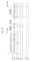
- Fig. 8 is a circuit diagram of one memory section 22, and Fig, 9 is a plan view showing the schematic layout of one memory section 22.
- a memory element 24 (24a-24d), which serves as the minimum memory unit, is composed of a sampling transistor 26 (26a-26d) connected to one pixel output line 141, a capacitor 25 (25a-25d) connected via the sampling transistor 26 to the pixel output line 141, and a reading transistor 27 (27a-27d) for reading an analogue voltage signal held in the capacitor 25.
- One memory section 22 consists of the combination of these four memory elements 24 (24a-24d). Accordingly, each memory section 22 can hold four different analogue voltage signals transferred from the same pixel through the same pixel output line 141.
- the signal output lines 23a, 23b, 23c and 23d via the four reading transistors 27a-27d are independent of each other, as shown in Figs, 8 and 9 .
- the memory elements 24a-24d can also be used in other operational modes. For example, if the storage capacitor 36 of each pixel 10 is not used, there is no need to consider the signal after an overflow and the noise signal contained in the signal after an overflow, in which case the memory elements 24 concerned can be used to increase the number of frames for continuous imaging. As a result, the possible number of frames for continuous imaging will be doubled to 208. If the noise removal is also unnecessary, the possible number of frames for continuous imaging will be further doubled to 416.
- the capacitors 25a-25d can be created, for example, by a double polysilicon gate structure or stack structure. Using a CCD structure to hold electric charges would cause the problem that an aliasing due to dark charges caused by thermal excitation or other factors would be added to the photo signal.
- the capacitors 25a-25d in the form of a double polysilicon gate structure or stack structure cause no such dark charges and hence no addition of aliasing, thus improving the S/N ratio of the signals to be extracted to the outside.
- the capacitors 25a-25d should preferably have a large capacitance per unit area. Accordingly, it is preferable to use an insulating film with a high dielectric constant. This choice reduces the area of the memory areas 3a and 3b and hence the chip area of the present solid-state image sensor. To increase the capacitance per unit area, the insulating films of the capacitors 25a-25d may have a non-planar structure, such as a trench structure.
- Fig. 10 is a block diagram showing a schematic configuration for reading signals held in the memory sections within the memory area 3a through the previously described signal output line 23.
- one memory section unit 20 is selected by a combination of the horizontal shift registers HSR1-HSR320 and vertical shift registers VSR1-VSR104.
- the memory sections 22 are sequentially selected to extract pixel signals one after another. It should be noted that understanding the reading operation requires considering only the operation inside one memory section unit block 50 since different memory section unit blocks 50 having separate output lines 23 can be concurrently operated.
- a process of performing a high-speed continuous imaging operation using the solid-state image sensor of the present invention is hereinafter described, where the process from the photoelectric conversion in each pixel 10 through the storage of the resultant signal in one memory section 22 is initially described with reference to Figs. 11 to 14 .
- the solid-stale image sensor of the present invention offers two different options for the drive mode: one drive mode is for a short photocharge storage time and the other for a relatively long photocharge storage time.
- the former mode is suitable for a photocharge storage time shorter than approximately 10 ⁇ sec, i.e. when the amount of dark charges produced by the floating diffusion can be regarded as negligible.
- This drive mode can be preferably used when the imaging is performed at a high rate of one million frames per second or higher.
- Fig. 11 is a drive timing chart of the operation mode for a short photocharge storage time
- Fig. 12 is a schematic potential diagram inside the pixel 10 during this drive mode.
- C PD , C FD and C CS denote the capacitances of the photodiode 31, floating diffusion 33 and storage capacitor 36, respectively
- C FD +C CS denotes the combined capacitance of the floating diffusion 33 and storage capacitor 36.
- the signal ⁇ X which is a common control signal supplied to every pixel 10
- the signals ⁇ T, ⁇ C and ⁇ R which are also common control signals, are set to a high level to turn on the transfer transistor 32, storage transistor 34 and reset transistor 35 (time t0), whereby the floating diffusion 33 and storage capacitor 36 are reset (or initialized).
- the photodiode 31 is completely depleted. The potential at this point in time is shown in Fig. 12(a) .
- ⁇ R is set to a low level to turn off the reset transistor 35, whereupon a noise signal N2, which equivalently contains a random noise generating in the floating diffusion 33 and storage capacitor 36 and a fixed pattern noise resulting from a variation in the threshold voltage of the transistor 37 in the source follower amplifier 43, is generated in the floating diffusion 33 (refer to Fig. 12(b) ), and an output current corresponding to this noise signal N2 flows through the pixel output line 141, At this timing (time t1), a sampling pulse ⁇ N2 is given to the memory section 22 to turn on the sampling transistor 26d so that the noise signal N2 outputted through the pixel output line 141 is held by the capacitor 25d.
- a noise signal N2 which equivalently contains a random noise generating in the floating diffusion 33 and storage capacitor 36 and a fixed pattern noise resulting from a variation in the threshold voltage of the transistor 37 in the source follower amplifier 43
- ⁇ C is set to the low level to turn off the storage transistor 34, whereupon the signal charges stored in the floating diffusion 33 and storage capacitor 36 at this point in time are distributed to the floating diffusion 33 and the storage capacitor 36 according to the ratio of their capacitances C FD and C CS (refer to Fig. 12(c) ).
- a noise signal N1 which contains a random noise generated when ⁇ C was turned off and a fixed pattern noise resulting from a variation in the threshold voltage of the transistor 37 in the source follower amplifier 43, is generated in the floating diffusion 33, and an output current corresponding to this noise signal N1 flows through the pixel output line 141.
- a sampling pulse ⁇ N1 is given to the memory section 22 to turn on the sampling transistor 26c so that the noise signal N1 outputted through the pixel output line 141 is held by the capacitor 25c.
- the transfer transistor 32 Since the transfer transistor 32 is maintained in the ON state, the photocharges generated by light falling onto the photodiode 31 flow through the transfer transistor 32 (this state is shown in Fig. 6(b) ) into the floating diffusion 33, and are stored in the floating diffusion 33, being superimposed on the noise signal N1 (time t3). If the floating diffusion 33 is saturated due to a large amount of photocharges produced in the photodiode 31 by an incidence of strong light, the overflowing charges are stored through the storage transistor 34 into the storage capacitor 36 (refer to Fig. 12(d) ). Setting the threshold voltage of the storage transistor 34 at an appropriately low level enables those charges to be efficiently transferred from the floating diffusion 33 to the storage capacitor 36.
- a sampling pulse ⁇ S1 is given to the memory section 22, with the storage transistor 34 in the OFF state, to turn on the sampling transistor 26a, whereby a signal corresponding to the charge stored in the floating diffusion 33 at that point in time (time t4) is extracted through the pixel output line 141 and held in the capacitor 25a (refer to Fig. 12(e) ).
- the signal stored in the floating diffusion 33 at this point in time results from the superposition of a noise signal N1 and a signal S1 corresponding to the charge before an overflow. Accordingly, the signal held in the capacitor 25a equals S1+N1, which does not reflect the amount of charge stored in the storage capacitor 36.
- ⁇ C is set to the high level to turn on the storage transistor 34, whereupon the charge held in the floating diffusion 33 at that point in time is mixed with the charge held in the storage capacitor 36 (refer to Fig. 12(f) ).
- a sampling pulse ⁇ S2 is given to the memory section 22 to turn on the sampling transistor 26b (time t5), whereby a signal corresponding to the charges held in the floating diffusion 33 and the storage capacitor 36, i.e. a signal resulting from the superposition of the noise signal N2 and the signal S2 corresponding to the charge after the overflow, is extracted through the pixel output line 141 and held in the capacitor 25b.
- the signal to be held in the capacitor 25b is S2+N2, which reflects the amount of charge stored in the storage capacitor 36.
- the signals S1+N1, S2+N2, N1 and N2 are respectively held in the four capacitors 25a, 25b, 25c and 25d included in one memory section 22.
- the noise signals N1 and N2 containing the random noise and fixed pattern noise are obtained separately from the other signals containing these noise signals. Therefore, it is possible to obtain high S/N image signals free from the influence of the noise signals N1 and N2 by reading each of these signals from the capacitors 25a, 25b, 25c and 25d and then subjecting the read signals to a subtracting operation.
- Fig. 13 is a drive timing chart in the case where the photocharge storage time is relatively long
- Fig. 14 is a schematic potential diagram inside the pixel in this operation.
- the transfer transistor 32 is turned off during the photocharge storage period so that the photocharges produced in the photodiode 31 will be stored in a depletion layer; the transfer transistor 32 is turned off during the photocharge storage period, and the sampling of the noise signal N1 is performed at the end of the photocharge storage period so that the dark charges (and photocharges) that generate in the floating diffusion 33 will not be included in the signal S1
- the purpose of turning off the transfer transistor 32 is to create an accumulation state at the interface between the silicon and insulating film immediately below its gate, thus filling the silicon surface with holes to prevent intrusion of dark charges through the interface between the silicon and insulating film.
- Another difference is that, taking into account the long photocharge storage time, the selection transistors 38 and 41 of the source follower amplifier 43 are turned off for a predetermined period of time to reduce the power consumption.
- ⁇ T, ⁇ C and ⁇ R are set to high levels to turn on both the storage, transistor 34 and reset transistor 35 (time t10), whereby the floating diffusion 33 and storage capacitor 36 are reset (or initialized).
- time t10 the floating diffusion 33 and storage capacitor 36 are reset (or initialized).
- the photodiode 31 is completely depleted.
- the state of potential at this point in time is shown in Fig. 14(a) .
- ⁇ R is set to the low level to turn off the reset, transistor 35, whereupon a noise signal N2, which equivalently contains a random noise generating in the floating diffusion 33 and the storage capacitor 36 and a fixed pattern noise resulting from a variation in the threshold voltage of the transistor 37 in the source follower amplifier 43, is generated in the floating diffusion 33 (refer to Fig. 14(b) ), and an output current corresponding to this noise signal N2 flows through the pixel output line 141.
- a sampling pulse ⁇ N2 is given to the memory section 22 to turn on the sampling transistor 26d, whereby the noise signal N2 is extracted through the pixel output line 141 and held in the capacitor 25d.
- ⁇ C is set to the low level to turn off the storage transistor 34, whereupon the signal charges stored in the floating diffusion is and storage capacitor 36 at this point in time are distributed to the floating diffusion 33 and storage capacitor 36 according to the ratio of their capacitances C FD and C CS .
- ⁇ T is set to the low level to turn off the transfer transistor 32
- ⁇ X is also set to the low level to turn off the two selection transistors 38 and 41 of the source follower amplifier 43 (time t12).
- a potential barrier is formed between the photodiode 31 and the floating diffusion 33, creating a condition where photocharges can be stored in the photodiode 31 (refer to Fig. 14(c) ).
- the photocharges produced by incident light falling onto the photodiode 31 are stored in the capacitance C PD of the photodiode 31.
- C PD capacitance of the photodiode 31.
- excessive charges flow through the transfer transistor 32, to be stored in the floating diffusion 33 and superimposed on the noise signal that has been distributed as described previously. If the floating diffusion 33 is saturated by stronger incident light, the charges will be stored through the storage transistor 34 into the storage capacitor 36 (refer to Fig. 14(d) ).
- ⁇ N is set to the high level to turn on the selection transistors 38 and 41, after which a sampling pulse ⁇ N1 is given to the memory section 22 to turn on the sampling transistor 26c, whereby a noise signal N1 corresponding to the signal charge stored in the floating diffusion 33 at this point in time (time t13) is extracted through the pixel output line 14 and held in the capacitor 25c.
- the noise signal N1 at this point in time contains a fixed pattern noise due to a variation in the threshold voltage of the transistor 37 in the source follower amplifier 43. It should be noted that this signal contains not only the noise but also a portion of the photocharges produced by photoelectric conversion, which are also regarded as a noise in the present case.
- ⁇ T is set to the high level to turn on the transfer transistor 32, whereupon the photocharges stored in the photodiode 31 are completely transferred to the floating diffusion 33 (refer to Fig. 14 (e.)).
- a sampling pulse ⁇ S1 is given to the memory section 22 to turn on the sampling transistor 26a, whereby a signal corresponding to the charge stored in the floating diffusion 33 is extracted through the pixel output line 14 and held in the capacitor 25a.
- This signal results from the superposition of the aforementioned noise signal N1 and the signal corresponding to the charge stored in the photodiode 31, i.e. the signal S1 before the overflow, and hence equals S 1+N1.
- ⁇ C is set to the high level to turn on the storage transistor 34, whereupon the charge held in the floating diffusion 33 at that point in time is mixed with the charge held in the storage capacitor 36 (refer to Fig. 14(f) ).
- a sampling pulse ⁇ S2 is given to the memory section 22 to turn on the sampling transistor 26b (time t15), whereby a signal corresponding to the charges held in the floating diffusion 33 and storage capacitor 36 are extracted through the pixel output line 141 and held in the capacitor 25b. This signal equals S2+N2.
- the signals S1+N1, S2+N2, N1 and N2 are respectively held in the four capacitors 25a, 25b, 25c and 25d included in one memory section 22.
- the noise signals N1 and N2 containing the random noise and fixed pattern noise are obtained separately from the other signals containing these noise signals. Therefore, it is possible to obtain high S/N images signals free from the influence of the noise signals N1 and N2 by reading each of these signals from the capacitors 25a, 25b, 25c and 25d and then subjecting the read signals to a subtracting operation. Since the charges that have overflowed from the floating diffusion 33 are not discarded but utilized, even a strong incident light barely causes saturation, so that the resultant signal can reflect the light. Thus, a wide dynamic range is ensured.
- the control signals ⁇ X, ⁇ T, ⁇ R and ⁇ C supplied to each pixel 10 are common to all the pixels. Therefore, the aforementioned operations of storing photocharges and transferring signals from each pixel 10 to the memory section 22 are simultaneously performed at all the pixels 10. That is, by one cycle of these operations, one frame of images signals are held in the 320 Memory sections 22 horizontally arranged in the memory area 3a shown in Fig. 3 . The operations are repeated 104 cycles to store the image signals in the memory sections 22 in all the memory section units 20. In the 105 th and subsequent cycles, the operation of writing signals in the memory sections 22 is once more initiated from the topmost memory section units 20. Thus, the signal-holding operation is cyclically carried out.
- This process is continued, for example, until a command signal four discontinuing the imaging is externally given.
- the command signal for discontinuing the imaging is given and the imaging is thereby discontinued, the latest 104 frames of image signals are held in the memory areas 3a and 3b. By sequentially reading these signals, a series of image signals corresponding to 104 frames can be obtained.
- a transistor for resetting is connected to each pixel output line 141.
- the sampling transistor 26 of the memory section 22 is turned on and, simultaneously, the transistor for resetting connected to the corresponding pixel output line 141 is turned on, whereby the signal stored in the capacitor 25 is reset through the sampling transistor 26 and the pixel output line 141. After this resetting operation is performed, a new signal is held in the capacitor 25.
- the signals held in the capacitors 25 of each memory section 22 are read by sequentially turning on the reading transistors 27 connected to the same signal output line 23. Since the four reading transistors 27a-27d of the same memory section 22 are respectively connected to the different signal output lines 23a-23d, the signals held in each of the four capacitors 25a-25d in the same memory section 22 can be simultaneously read. Using these signals, the subtracting operations of (S1+N1)-N1 and (S2+N2)-N2 can be performed by a subtraction circuit (now shown) provided inside or outside the sensor to extract each of the signals S1 and S2 free from the random noise and fixed pattern noise.
- Which of S1 and S2 should be used is determine with reference to an appropriate signal level (threshold value) equal to or lower than the saturation level of the signal S1; S1 is selected when the signal is equal to or higher than the reference level, and S2 when the signal is lower than the reference level. By performing this selection below the signal saturation level, it is possible to avoid the influence of saturation variation of the signal S 1.
- Fig. 15 is an operation timing chart of sequential reading of the signals from the memory areas 3a and 3b
- Fig. 16 is an operation timing chart of the main portion of the horizontal shift registers HSR
- Fig. 17 an operation timing chart of the main portion of the vertical shift registers VSR.
- the reading order at the leftmost memory section unit block 50 in the 320 memory section units 20 corresponding to the first frame in Fig. 10 is hereinafter described.
- image signals of eleven pixels are sequentially read from the memory sections 22 in the left-to-right direction of the first horizontal row shown in Fig. 7 .
- This memory section unit 20-01 is selected by activating the horizontal shift register HSR1 and vertical shift register VSH1.
- the horizontal reading clock H-CLK. produces a moving pulse signal that turns on the reading transistors 27 of the memory sections 22, one by one, from left to right in the horizontal direction.
- the signals y1, y2 and y3 in Fig. 16 are one example of this pulse signal.
- a clock V-CLK for shifting the vertical reading position is supplied, whereby the memory sections 22 in the next (second) row are selected. Then, these memory sections 22 are similarly selected, from left to right, for the reading of eleven pixels. Such a process of reading pixel signals is repeated until the end of the twelfth row.
- the signals v1, v2 and v3 shown in Fig. 17 are one example of the signal for activating the reading transistor 27 corresponding to each row in the vertical direction.
- the horizontal shift register HSR2 and vertical shift register VSR1 are activated to select the memory section unit 20-02 on the right, and this memory section unit 20-02 becomes the target of reading, as shown in Fig 16 .
- the signals are read by turning on the reading transistors 27 of each memory section 22, for one pixel after another, in the order of row ⁇ column.
- the sequential selection of each memory section unit 20 is continued until the memory section unit 20-10.
- the reading process for one frame is completed.
- the other memory section unit blocks 50 the operation of reading signals from the memory sections of the corresponding memory section units is similarly performed.
- the reading of pixel signals of the second frame is subsequently initiated. That is, as shown in Fig. 16 , the horizontal shift register HSR1 and the vertical shift register VSR2 are activated to select the leftmost memory section unit of the second row shown in Fig. 10 , and the reading operation is performed in the same order as in the case of the first frame. This process is repeated to perform the reading operation through the end of the 104 th frame. It should be noted that the reading process is not specifically limited to this one; it can be appropriately modified.
- the pixel output lines 14 may be arranged over the photoelectric conversion area 11. Furthermore, to increase the concentration ratio, a plurality of on-chip micro-lenses approximately shaped like a partial sphere or partial cylinder may be arranged on the pixel output lines 14 so that these lenses form images between the pixel output lines 14.
- the pixel area 2 (2a and 2b) and memory areas 3a and 3b are each formed as an independent area and separately located on the same surface of the semiconductor substrate 1.
- a structure with a light incidence surface on the back side may be adopted. That is, the separation of the pixel area 2 (2a and 2b) and memory areas 3a and 3b may be achieved, for example, by a structure in which the light incidence surface with a two-dimensional array of the photodiodes 31 is provided on the side opposite from the pattern surface on which the transistors and other elements are formed.
- the pixel area 2 (2a and 2b) and memory areas 3a and 3b may be individually formed on separate semiconductor chips, rather than on the same semiconductor chip, and connected together by a generally known method. Specifically, it is possible to mount different semiconductor chips on separate substrates and connect them by wire-bonding for their signal exchange. Alternatively, a plurality of semiconductor chips may be vertically stacked, rather than horizontally arranged, and connected by flip-chip mounting or other techniques so that they can exchange signals.
Applications Claiming Priority (2)
| Application Number | Priority Date | Filing Date | Title |
|---|---|---|---|
| JP2007230178 | 2007-09-05 | ||
| PCT/JP2008/002425 WO2009031301A1 (ja) | 2007-09-05 | 2008-09-04 | 固体撮像素子 |
Publications (3)
| Publication Number | Publication Date |
|---|---|
| EP2190185A1 true EP2190185A1 (de) | 2010-05-26 |
| EP2190185A4 EP2190185A4 (de) | 2010-08-18 |
| EP2190185B1 EP2190185B1 (de) | 2013-11-06 |
Family
ID=40428625
Family Applications (1)
| Application Number | Title | Priority Date | Filing Date |
|---|---|---|---|
| EP08829399.8A Active EP2190185B1 (de) | 2007-09-05 | 2008-09-04 | Festkörperabbildungselement |
Country Status (7)
| Country | Link |
|---|---|
| US (1) | US8988571B2 (de) |
| EP (1) | EP2190185B1 (de) |
| JP (1) | JP4931160B2 (de) |
| KR (1) | KR101126322B1 (de) |
| CN (1) | CN101796822A (de) |
| TW (1) | TW200922308A (de) |
| WO (1) | WO2009031301A1 (de) |
Cited By (1)
| Publication number | Priority date | Publication date | Assignee | Title |
|---|---|---|---|---|
| DE102019101752A1 (de) | 2018-02-05 | 2019-08-08 | pmdtechnologies ag | Pixelarray für eine Kamera, Kamera und Lichtlaufzeitkamerasystem mit einer derartigen Kamera |
Families Citing this family (30)
| Publication number | Priority date | Publication date | Assignee | Title |
|---|---|---|---|---|
| US8569805B2 (en) * | 2007-09-05 | 2013-10-29 | Tohoku University | Solid-state image sensor and method for producing the same |
| CN102057666B (zh) | 2008-06-10 | 2014-04-02 | 国立大学法人东北大学 | 固体摄像元件 |
| JP5674350B2 (ja) | 2009-07-10 | 2015-02-25 | 株式会社島津製作所 | 固体撮像素子 |
| JP2011233949A (ja) * | 2010-04-23 | 2011-11-17 | Olympus Corp | 撮像装置 |
| JP5709404B2 (ja) * | 2010-05-10 | 2015-04-30 | キヤノン株式会社 | 固体撮像装置およびその駆動方法 |
| JP4657379B1 (ja) * | 2010-09-01 | 2011-03-23 | 株式会社ナックイメージテクノロジー | 高速度ビデオカメラ |
| WO2012107995A1 (ja) | 2011-02-08 | 2012-08-16 | 国立大学法人東北大学 | 固体撮像素子及びその駆動方法 |
| KR101251744B1 (ko) * | 2011-04-13 | 2013-04-05 | 엘지이노텍 주식회사 | Wdr 픽셀 어레이, 이를 포함하는 wdr 이미징 장치 및 그 구동방법 |
| JP2013015357A (ja) * | 2011-07-01 | 2013-01-24 | Shimadzu Corp | フローサイトメータ |
| US8836626B2 (en) | 2011-07-15 | 2014-09-16 | Semiconductor Energy Laboratory Co., Ltd. | Semiconductor device and method for driving the same |
| JP5959187B2 (ja) * | 2011-12-02 | 2016-08-02 | オリンパス株式会社 | 固体撮像装置、撮像装置、および信号読み出し方法 |
| US9007504B2 (en) * | 2012-04-06 | 2015-04-14 | Omnivision Technologies, Inc. | Method, apparatus and system for reducing pixel cell noise |
| JP6042636B2 (ja) * | 2012-05-28 | 2016-12-14 | オリンパス株式会社 | 固体撮像素子および固体撮像装置 |
| EP2890117B1 (de) | 2013-12-26 | 2020-11-18 | IMEC vzw | Verbesserungen in und im Zusammenhang mit Bildsensoren |
| TWI648986B (zh) * | 2014-04-15 | 2019-01-21 | 日商新力股份有限公司 | 攝像元件、電子機器 |
| JP6218799B2 (ja) | 2015-01-05 | 2017-10-25 | キヤノン株式会社 | 撮像素子及び撮像装置 |
| US10070088B2 (en) * | 2015-01-05 | 2018-09-04 | Canon Kabushiki Kaisha | Image sensor and image capturing apparatus for simultaneously performing focus detection and image generation |
| JP6512291B2 (ja) * | 2015-07-06 | 2019-05-15 | 株式会社島津製作所 | 固体撮像素子の信号処理方法及び駆動方法 |
| GB2544333B (en) * | 2015-11-13 | 2018-02-21 | Advanced Risc Mach Ltd | Display controller |
| JP6842240B2 (ja) | 2016-03-07 | 2021-03-17 | 株式会社リコー | 画素ユニット、及び撮像素子 |
| US10879298B2 (en) * | 2016-03-24 | 2020-12-29 | Nikon Corporation | Image sensor and image capturing device |
| JP6789678B2 (ja) * | 2016-06-06 | 2020-11-25 | キヤノン株式会社 | 撮像装置、撮像システム |
| DE102016212765A1 (de) * | 2016-07-13 | 2018-01-18 | Robert Bosch Gmbh | Pixeleinheit für einen Bildsensor, Bildsensor, Verfahren zum Sensieren eines Lichtsignals, Verfahren zum Ansteuern einer Pixeleinheit und Verfahren zum Generieren eines Bildes unter Verwendung einer Pixeleinheit |
| TWI754696B (zh) * | 2016-12-14 | 2022-02-11 | 日商索尼半導體解決方案公司 | 固體攝像元件及電子機器 |
| KR102427832B1 (ko) | 2017-04-12 | 2022-08-02 | 삼성전자주식회사 | 이미지 센서 |
| CN113614565B (zh) * | 2019-03-29 | 2024-03-08 | 凸版印刷株式会社 | 固体摄像装置、摄像系统及摄像方法 |
| DE102019113597B3 (de) | 2019-05-22 | 2020-08-06 | pmdtechnologies ag | Pixelarray für eine Kamera, Kamera und Lichtlaufzeitkamerasystem mit einer derartigen Kamera |
| KR20210059469A (ko) * | 2019-11-15 | 2021-05-25 | 삼성전자주식회사 | 픽셀 어레이 및 이를 포함하는 이미지 센서 |
| JP7330124B2 (ja) * | 2020-03-19 | 2023-08-21 | 株式会社東芝 | 固体撮像装置 |
| JP7030929B2 (ja) * | 2020-11-04 | 2022-03-07 | キヤノン株式会社 | 撮像装置、撮像システム |
Citations (3)
| Publication number | Priority date | Publication date | Assignee | Title |
|---|---|---|---|---|
| US5872484A (en) * | 1997-07-11 | 1999-02-16 | Texas Instruments Incorporated | High performance current output amplifier for CCD image sensors |
| US5990951A (en) * | 1996-10-09 | 1999-11-23 | Sharp Kabushiki Kaisha | Solid-state imaging device and method for driving the same |
| US20030052983A1 (en) * | 2001-09-17 | 2003-03-20 | Michael Altree | Image capture and storage device |
Family Cites Families (23)
| Publication number | Priority date | Publication date | Assignee | Title |
|---|---|---|---|---|
| JPS63174356A (ja) | 1987-01-14 | 1988-07-18 | Agency Of Ind Science & Technol | 画像処理用半導体装置 |
| US6787749B1 (en) * | 1996-11-12 | 2004-09-07 | California Institute Of Technology | Integrated sensor with frame memory and programmable resolution for light adaptive imaging |
| US6078037A (en) | 1998-04-16 | 2000-06-20 | Intel Corporation | Active pixel CMOS sensor with multiple storage capacitors |
| US7139025B1 (en) * | 1998-10-29 | 2006-11-21 | Micron Technology, Inc. | Active pixel sensor with mixed analog and digital signal integration |
| US6429036B1 (en) * | 1999-01-14 | 2002-08-06 | Micron Technology, Inc. | Backside illumination of CMOS image sensor |
| US6307243B1 (en) * | 1999-07-19 | 2001-10-23 | Micron Technology, Inc. | Microlens array with improved fill factor |
| JP3704052B2 (ja) | 2000-03-28 | 2005-10-05 | リンク・リサーチ株式会社 | 高速撮像素子及び高速撮影装置 |
| US6985181B2 (en) * | 2000-05-09 | 2006-01-10 | Pixim, Inc. | CMOS sensor array with a memory interface |
| JP3846572B2 (ja) * | 2001-09-20 | 2006-11-15 | ソニー株式会社 | 固体撮像装置 |
| JP4466612B2 (ja) | 2001-09-20 | 2010-05-26 | ソニー株式会社 | 固体撮像装置及びその制御方法 |
| US7071982B2 (en) * | 2001-10-24 | 2006-07-04 | Texas Instruments Incorporated | Adaptive relative and absolute address coding CMOS imager technique and system architecture |
| US20030206236A1 (en) * | 2002-05-06 | 2003-11-06 | Agfa Corporation | CMOS digital image sensor system and method |
| JP4601897B2 (ja) * | 2002-11-13 | 2010-12-22 | ソニー株式会社 | 固体撮像装置及びその駆動方法 |
| US20040125093A1 (en) * | 2002-12-30 | 2004-07-01 | Serge Rutman | Micro-controller with integrated light modulator |
| JP2005303621A (ja) * | 2004-04-09 | 2005-10-27 | Link Research Kk | 高速撮像装置 |
| JP2006101479A (ja) * | 2004-09-02 | 2006-04-13 | Canon Inc | 固体撮像装置及びそれを用いたカメラ |
| US7817193B2 (en) | 2004-11-25 | 2010-10-19 | Sony Corporation | Image pickup apparatus and image pickup method to display or record images picked up at high rate in real time |
| JP5066704B2 (ja) | 2005-02-04 | 2012-11-07 | 国立大学法人東北大学 | 固体撮像装置、および固体撮像装置の動作方法 |
| JP4561439B2 (ja) * | 2005-03-30 | 2010-10-13 | 株式会社デンソー | 撮像装置 |
| KR100682829B1 (ko) | 2005-05-18 | 2007-02-15 | 삼성전자주식회사 | 씨모스 이미지 센서의 단위 픽셀, 픽셀 어레이 및 이를포함한 씨모스 이미지 센서 |
| JP2007166581A (ja) | 2005-11-16 | 2007-06-28 | Matsushita Electric Ind Co Ltd | 高速撮影用固体撮像装置 |
| JP4745876B2 (ja) * | 2006-03-29 | 2011-08-10 | キヤノン株式会社 | 画像処理装置及び画像処理方法 |
| JP4293210B2 (ja) * | 2006-08-18 | 2009-07-08 | ソニー株式会社 | 物理量検出装置、物理量検出装置の駆動方法、固体撮像装置、固体撮像装置の駆動方法、及び撮像装置 |
-
2008
- 2008-09-04 WO PCT/JP2008/002425 patent/WO2009031301A1/ja active Application Filing
- 2008-09-04 US US12/676,562 patent/US8988571B2/en active Active
- 2008-09-04 EP EP08829399.8A patent/EP2190185B1/de active Active
- 2008-09-04 JP JP2009531123A patent/JP4931160B2/ja active Active
- 2008-09-04 CN CN200880105558A patent/CN101796822A/zh active Pending
- 2008-09-04 KR KR1020107003063A patent/KR101126322B1/ko active IP Right Grant
- 2008-09-05 TW TW097134047A patent/TW200922308A/zh unknown
Patent Citations (3)
| Publication number | Priority date | Publication date | Assignee | Title |
|---|---|---|---|---|
| US5990951A (en) * | 1996-10-09 | 1999-11-23 | Sharp Kabushiki Kaisha | Solid-state imaging device and method for driving the same |
| US5872484A (en) * | 1997-07-11 | 1999-02-16 | Texas Instruments Incorporated | High performance current output amplifier for CCD image sensors |
| US20030052983A1 (en) * | 2001-09-17 | 2003-03-20 | Michael Altree | Image capture and storage device |
Non-Patent Citations (2)
| Title |
|---|
| CHEN Y ET AL: "High-Speed CMOS Image Sensor Circuits With In Situ Frame Storage" IEEE TRANSACTIONS ON NUCLEAR SCIENCE, IEEE SERVICE CENTER, NEW YORK, NY, US LNKD- DOI:10.1109/TNS.2004.832584, vol. 51, no. 4, 1 August 2004 (2004-08-01) , pages 1648-1656, XP011116239 ISSN: 0018-9499 * |
| See also references of WO2009031301A1 * |
Cited By (1)
| Publication number | Priority date | Publication date | Assignee | Title |
|---|---|---|---|---|
| DE102019101752A1 (de) | 2018-02-05 | 2019-08-08 | pmdtechnologies ag | Pixelarray für eine Kamera, Kamera und Lichtlaufzeitkamerasystem mit einer derartigen Kamera |
Also Published As
| Publication number | Publication date |
|---|---|
| TW200922308A (en) | 2009-05-16 |
| CN101796822A (zh) | 2010-08-04 |
| WO2009031301A1 (ja) | 2009-03-12 |
| EP2190185A4 (de) | 2010-08-18 |
| JPWO2009031301A1 (ja) | 2010-12-09 |
| US8988571B2 (en) | 2015-03-24 |
| EP2190185B1 (de) | 2013-11-06 |
| US20100208115A1 (en) | 2010-08-19 |
| JP4931160B2 (ja) | 2012-05-16 |
| KR20100038446A (ko) | 2010-04-14 |
| KR101126322B1 (ko) | 2012-07-12 |
Similar Documents
| Publication | Publication Date | Title |
|---|---|---|
| EP2190185B1 (de) | Festkörperabbildungselement | |
| US8569805B2 (en) | Solid-state image sensor and method for producing the same | |
| US8541731B2 (en) | Solid-state image sensor | |
| EP2665256B1 (de) | Festkörperbildsensor und Ansteuerverfahren dafür | |
| US9420210B2 (en) | Solid-state image sensor for capturing high-speed phenomena and drive method for the same | |
| US8269838B2 (en) | Solid-state image sensor and imaging device | |
| JP6570384B2 (ja) | 撮像装置及び撮像システム | |
| US8816266B2 (en) | Solid-state imaging device, method for driving solid-state imaging device, and electronic apparatus | |
| JP4267095B2 (ja) | 共有された増幅器読出しを有する能動画素画像センサ | |
| JP5458582B2 (ja) | 固体撮像装置、固体撮像装置の駆動方法および電子機器 | |
| US9402038B2 (en) | Solid-state imaging device and method of driving comprising a first and second accumulation sections for transferring charges exceeding the saturation amount | |
| JP2006093816A (ja) | 固体撮像装置 | |
| JP6412347B2 (ja) | 画素回路およびこれを搭載した撮像装置 |
Legal Events
| Date | Code | Title | Description |
|---|---|---|---|
| PUAI | Public reference made under article 153(3) epc to a published international application that has entered the european phase |
Free format text: ORIGINAL CODE: 0009012 |
|
| 17P | Request for examination filed |
Effective date: 20100322 |
|
| AK | Designated contracting states |
Kind code of ref document: A1 Designated state(s): AT BE BG CH CY CZ DE DK EE ES FI FR GB GR HR HU IE IS IT LI LT LU LV MC MT NL NO PL PT RO SE SI SK TR |
|
| AX | Request for extension of the european patent |
Extension state: AL BA MK RS |
|
| A4 | Supplementary search report drawn up and despatched |
Effective date: 20100719 |
|
| DAX | Request for extension of the european patent (deleted) | ||
| 17Q | First examination report despatched |
Effective date: 20111227 |
|
| GRAP | Despatch of communication of intention to grant a patent |
Free format text: ORIGINAL CODE: EPIDOSNIGR1 |
|
| INTG | Intention to grant announced |
Effective date: 20130605 |
|
| GRAS | Grant fee paid |
Free format text: ORIGINAL CODE: EPIDOSNIGR3 |
|
| GRAA | (expected) grant |
Free format text: ORIGINAL CODE: 0009210 |
|
| AK | Designated contracting states |
Kind code of ref document: B1 Designated state(s): AT BE BG CH CY CZ DE DK EE ES FI FR GB GR HR HU IE IS IT LI LT LU LV MC MT NL NO PL PT RO SE SI SK TR |
|
| REG | Reference to a national code |
Ref country code: GB Ref legal event code: FG4D |
|
| REG | Reference to a national code |
Ref country code: CH Ref legal event code: EP |
|
| REG | Reference to a national code |
Ref country code: AT Ref legal event code: REF Ref document number: 640085 Country of ref document: AT Kind code of ref document: T Effective date: 20131215 |
|
| REG | Reference to a national code |
Ref country code: IE Ref legal event code: FG4D |
|
| REG | Reference to a national code |
Ref country code: DE Ref legal event code: R096 Ref document number: 602008028629 Country of ref document: DE Effective date: 20140102 |
|
| REG | Reference to a national code |
Ref country code: NL Ref legal event code: T3 |
|
| REG | Reference to a national code |
Ref country code: NL Ref legal event code: T3 |
|
| REG | Reference to a national code |
Ref country code: AT Ref legal event code: MK05 Ref document number: 640085 Country of ref document: AT Kind code of ref document: T Effective date: 20131106 |
|
| REG | Reference to a national code |
Ref country code: LT Ref legal event code: MG4D |
|
| PG25 | Lapsed in a contracting state [announced via postgrant information from national office to epo] |
Ref country code: SE Free format text: LAPSE BECAUSE OF FAILURE TO SUBMIT A TRANSLATION OF THE DESCRIPTION OR TO PAY THE FEE WITHIN THE PRESCRIBED TIME-LIMIT Effective date: 20131106 Ref country code: IS Free format text: LAPSE BECAUSE OF FAILURE TO SUBMIT A TRANSLATION OF THE DESCRIPTION OR TO PAY THE FEE WITHIN THE PRESCRIBED TIME-LIMIT Effective date: 20140306 Ref country code: LT Free format text: LAPSE BECAUSE OF FAILURE TO SUBMIT A TRANSLATION OF THE DESCRIPTION OR TO PAY THE FEE WITHIN THE PRESCRIBED TIME-LIMIT Effective date: 20131106 Ref country code: FI Free format text: LAPSE BECAUSE OF FAILURE TO SUBMIT A TRANSLATION OF THE DESCRIPTION OR TO PAY THE FEE WITHIN THE PRESCRIBED TIME-LIMIT Effective date: 20131106 Ref country code: HR Free format text: LAPSE BECAUSE OF FAILURE TO SUBMIT A TRANSLATION OF THE DESCRIPTION OR TO PAY THE FEE WITHIN THE PRESCRIBED TIME-LIMIT Effective date: 20131106 Ref country code: NO Free format text: LAPSE BECAUSE OF FAILURE TO SUBMIT A TRANSLATION OF THE DESCRIPTION OR TO PAY THE FEE WITHIN THE PRESCRIBED TIME-LIMIT Effective date: 20140206 |
|
| PG25 | Lapsed in a contracting state [announced via postgrant information from national office to epo] |
Ref country code: ES Free format text: LAPSE BECAUSE OF FAILURE TO SUBMIT A TRANSLATION OF THE DESCRIPTION OR TO PAY THE FEE WITHIN THE PRESCRIBED TIME-LIMIT Effective date: 20131106 Ref country code: BE Free format text: LAPSE BECAUSE OF FAILURE TO SUBMIT A TRANSLATION OF THE DESCRIPTION OR TO PAY THE FEE WITHIN THE PRESCRIBED TIME-LIMIT Effective date: 20131106 Ref country code: AT Free format text: LAPSE BECAUSE OF FAILURE TO SUBMIT A TRANSLATION OF THE DESCRIPTION OR TO PAY THE FEE WITHIN THE PRESCRIBED TIME-LIMIT Effective date: 20131106 Ref country code: LV Free format text: LAPSE BECAUSE OF FAILURE TO SUBMIT A TRANSLATION OF THE DESCRIPTION OR TO PAY THE FEE WITHIN THE PRESCRIBED TIME-LIMIT Effective date: 20131106 |
|
| PG25 | Lapsed in a contracting state [announced via postgrant information from national office to epo] |
Ref country code: PT Free format text: LAPSE BECAUSE OF FAILURE TO SUBMIT A TRANSLATION OF THE DESCRIPTION OR TO PAY THE FEE WITHIN THE PRESCRIBED TIME-LIMIT Effective date: 20140306 |
|
| PG25 | Lapsed in a contracting state [announced via postgrant information from national office to epo] |
Ref country code: EE Free format text: LAPSE BECAUSE OF FAILURE TO SUBMIT A TRANSLATION OF THE DESCRIPTION OR TO PAY THE FEE WITHIN THE PRESCRIBED TIME-LIMIT Effective date: 20131106 |
|
| REG | Reference to a national code |
Ref country code: DE Ref legal event code: R097 Ref document number: 602008028629 Country of ref document: DE |
|
| PG25 | Lapsed in a contracting state [announced via postgrant information from national office to epo] |
Ref country code: CZ Free format text: LAPSE BECAUSE OF FAILURE TO SUBMIT A TRANSLATION OF THE DESCRIPTION OR TO PAY THE FEE WITHIN THE PRESCRIBED TIME-LIMIT Effective date: 20131106 Ref country code: PL Free format text: LAPSE BECAUSE OF FAILURE TO SUBMIT A TRANSLATION OF THE DESCRIPTION OR TO PAY THE FEE WITHIN THE PRESCRIBED TIME-LIMIT Effective date: 20131106 Ref country code: RO Free format text: LAPSE BECAUSE OF FAILURE TO SUBMIT A TRANSLATION OF THE DESCRIPTION OR TO PAY THE FEE WITHIN THE PRESCRIBED TIME-LIMIT Effective date: 20131106 Ref country code: SK Free format text: LAPSE BECAUSE OF FAILURE TO SUBMIT A TRANSLATION OF THE DESCRIPTION OR TO PAY THE FEE WITHIN THE PRESCRIBED TIME-LIMIT Effective date: 20131106 Ref country code: IT Free format text: LAPSE BECAUSE OF FAILURE TO SUBMIT A TRANSLATION OF THE DESCRIPTION OR TO PAY THE FEE WITHIN THE PRESCRIBED TIME-LIMIT Effective date: 20131106 |
|
| PLBE | No opposition filed within time limit |
Free format text: ORIGINAL CODE: 0009261 |
|
| STAA | Information on the status of an ep patent application or granted ep patent |
Free format text: STATUS: NO OPPOSITION FILED WITHIN TIME LIMIT |
|
| PG25 | Lapsed in a contracting state [announced via postgrant information from national office to epo] |
Ref country code: DK Free format text: LAPSE BECAUSE OF FAILURE TO SUBMIT A TRANSLATION OF THE DESCRIPTION OR TO PAY THE FEE WITHIN THE PRESCRIBED TIME-LIMIT Effective date: 20131106 |
|
| 26N | No opposition filed |
Effective date: 20140807 |
|
| REG | Reference to a national code |
Ref country code: DE Ref legal event code: R097 Ref document number: 602008028629 Country of ref document: DE Effective date: 20140807 |
|
| PG25 | Lapsed in a contracting state [announced via postgrant information from national office to epo] |
Ref country code: SI Free format text: LAPSE BECAUSE OF FAILURE TO SUBMIT A TRANSLATION OF THE DESCRIPTION OR TO PAY THE FEE WITHIN THE PRESCRIBED TIME-LIMIT Effective date: 20131106 |
|
| PG25 | Lapsed in a contracting state [announced via postgrant information from national office to epo] |
Ref country code: LU Free format text: LAPSE BECAUSE OF FAILURE TO SUBMIT A TRANSLATION OF THE DESCRIPTION OR TO PAY THE FEE WITHIN THE PRESCRIBED TIME-LIMIT Effective date: 20140904 Ref country code: MC Free format text: LAPSE BECAUSE OF FAILURE TO SUBMIT A TRANSLATION OF THE DESCRIPTION OR TO PAY THE FEE WITHIN THE PRESCRIBED TIME-LIMIT Effective date: 20131106 |
|
| REG | Reference to a national code |
Ref country code: CH Ref legal event code: PL |
|
| REG | Reference to a national code |
Ref country code: IE Ref legal event code: MM4A |
|
| PG25 | Lapsed in a contracting state [announced via postgrant information from national office to epo] |
Ref country code: CH Free format text: LAPSE BECAUSE OF NON-PAYMENT OF DUE FEES Effective date: 20140930 Ref country code: LI Free format text: LAPSE BECAUSE OF NON-PAYMENT OF DUE FEES Effective date: 20140930 |
|
| PG25 | Lapsed in a contracting state [announced via postgrant information from national office to epo] |
Ref country code: IE Free format text: LAPSE BECAUSE OF NON-PAYMENT OF DUE FEES Effective date: 20140904 |
|
| PG25 | Lapsed in a contracting state [announced via postgrant information from national office to epo] |
Ref country code: BG Free format text: LAPSE BECAUSE OF FAILURE TO SUBMIT A TRANSLATION OF THE DESCRIPTION OR TO PAY THE FEE WITHIN THE PRESCRIBED TIME-LIMIT Effective date: 20131106 |
|
| PG25 | Lapsed in a contracting state [announced via postgrant information from national office to epo] |
Ref country code: CY Free format text: LAPSE BECAUSE OF FAILURE TO SUBMIT A TRANSLATION OF THE DESCRIPTION OR TO PAY THE FEE WITHIN THE PRESCRIBED TIME-LIMIT Effective date: 20131106 Ref country code: GR Free format text: LAPSE BECAUSE OF FAILURE TO SUBMIT A TRANSLATION OF THE DESCRIPTION OR TO PAY THE FEE WITHIN THE PRESCRIBED TIME-LIMIT Effective date: 20140207 Ref country code: MT Free format text: LAPSE BECAUSE OF FAILURE TO SUBMIT A TRANSLATION OF THE DESCRIPTION OR TO PAY THE FEE WITHIN THE PRESCRIBED TIME-LIMIT Effective date: 20131106 |
|
| PG25 | Lapsed in a contracting state [announced via postgrant information from national office to epo] |
Ref country code: TR Free format text: LAPSE BECAUSE OF FAILURE TO SUBMIT A TRANSLATION OF THE DESCRIPTION OR TO PAY THE FEE WITHIN THE PRESCRIBED TIME-LIMIT Effective date: 20131106 Ref country code: HU Free format text: LAPSE BECAUSE OF FAILURE TO SUBMIT A TRANSLATION OF THE DESCRIPTION OR TO PAY THE FEE WITHIN THE PRESCRIBED TIME-LIMIT; INVALID AB INITIO Effective date: 20080904 |
|
| REG | Reference to a national code |
Ref country code: FR Ref legal event code: PLFP Year of fee payment: 9 |
|
| REG | Reference to a national code |
Ref country code: FR Ref legal event code: PLFP Year of fee payment: 10 |
|
| REG | Reference to a national code |
Ref country code: FR Ref legal event code: PLFP Year of fee payment: 11 |
|
| REG | Reference to a national code |
Ref country code: DE Ref legal event code: R079 Ref document number: 602008028629 Country of ref document: DE Free format text: PREVIOUS MAIN CLASS: H04N0005335000 Ipc: H04N0025000000 |
|
| PGFP | Annual fee paid to national office [announced via postgrant information from national office to epo] |
Ref country code: NL Payment date: 20230816 Year of fee payment: 16 |
|
| PGFP | Annual fee paid to national office [announced via postgrant information from national office to epo] |
Ref country code: GB Payment date: 20230727 Year of fee payment: 16 |
|
| PGFP | Annual fee paid to national office [announced via postgrant information from national office to epo] |
Ref country code: FR Payment date: 20230808 Year of fee payment: 16 Ref country code: DE Payment date: 20230802 Year of fee payment: 16 |